1
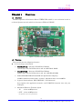
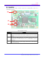
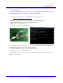
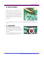
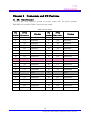
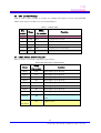
TOKUDEN Spartan-6 Evalutaion Board
(TKDN-SP6-16/45)
Hardware manual
Rev 3
August 10, 2010
Tokushu Denshi Kairo Inc.
特電
TOKUDEN
Notes
For safety using, please note the operating suggestions listed below. Failure to use
caution may lead to personal injury, fire, or property damage.
1. Take care not to damage, shock or be injured in touching the current-carrying
device.
2. When this product is inserted with wrong direction, it may have a serious
damage. Inserting and removing should be done under the power off.
3. Take care not to make impact, heating, or vibrate hardly.
4. When some trouble has found, power off and check the board.
This product is intended for education, preproduction and testing the FPGA’s behavior,
so that Tokushi Denshi Kairo Inc. assumes no responsibility for any results from other
usage, and couldn’t be applied to following high-risk application without written
pre-permission.
1. Instruments associated with human life.
2. Medical Equipment
3. Instruments which may affect natural environment, someone’s health or
belonging adversely by malfunction.
4. Instruments which may cause fire hazard by malfunction.
5. Aerospace instrument, and navigation system
6. Tactical weapon system, manufacture system or their helping system for
military purposes.
7. Instruments rerated nuclear power.
8. Electric power tools.
9. Other instruments which may cause some trouble and damage by occurring
malfunction or loss of data.
1
©Copyright 2009 特殊電子回路㈱ All rights reserved.
特電
TOKUDEN
Index
Introduction................................................エラー! ブックマークが定義されていません。
Chapter 1 Overview.......................................................................................................... 4
1.1
Overview.................................................................................................................. 4
1.2
Functional Description ........................................................................................... 4
1.3
Hardware Requirements......................................................................................... 5
Chapter 2 Setup................................................................................................................ 6
2.1
Connector Attachment ............................................................................................ 6
2.2
Power Supply........................................................................................................... 6
2.3
Jumper Setting........................................................................................................ 7
Chapter 3 Configuring the FPGA .................................................................................... 8
3.1
How to Configure .................................................................................................... 8
3.2
Using USB Cable..................................................................................................... 9
3.3
Using Other JTAG Cable ...................................................................................... 10
3.4
Reconfigure FPGA................................................................................................. 10
Chapter 4 DDR2-SDRAM............................................................................................... 11
Chapter 5 Connectors and I/O Features........................................................................ 12
5.1
CN1 (40pin Extender).................................................................................... 12
5.2
CN2 (40pin Extender).................................................................................... 13
5.3
CN5 (for SPI Writing) .................................................................................... 14
5.4
LEDs, Switch, Cristal Oscillator .......................................................................... 14
Chapter 6 Support .......................................................................................................... 15
2
©Copyright 2009 特殊電子回路㈱ All rights reserved.
特電
TOKUDEN
Introduction
Thank you for purchasing TOKUDEN Spartan-6 Evaluation Board (TKDN-SP6-16/45).
This product helps you a lot to develop your original control device using XILINX’s
newest FPGA ,Spartan-6.
Notice
1.This paper and product’s specification may change without preliminary announce
because of its improvement.
2.Tokusyu Denshi Kairo Inc. put the maximum effort into making this product, but if
you have detect some problem, please contact us.
3.Tokusyu Denshi Kairo Inc. assumes no responsibility for any results from whatever
usage.
Components
This package includes :
Tokuden Spartan-6 Evaluation Board 1
Accessories
Pinheader (40 pin)
2
DC Power Jack
1
This board requires MiniB USB cable to configure FPGA by JTAG. You need not to
prepare JTAG cable.
3
©Copyright 2009 特殊電子回路㈱ All rights reserved.
特電
TOKUDEN
Chapter 1
1.1
Overview
Overview
Tokuden Spartan-6 Evaluation Board (TKDN-SP6-16/45) is an evaluation board to
evaluate Spartan-6 easily which is the newest FPGA of XILINX.
Figure 1 Top View of the TKDN-SP6-16/45
1.2
Features
This product has the following features.
It carries large-scale FPGA
TKDN-SP6-16
Spartan-6 XC6SLX16-CSG324
14,579 logic cells, 32 DSP48 slices and 32 18kB Block RAMs
TKDN-SP6-45
Spartan-6 XC6SLX45-CSG324
43,661 logic cells, 58 DSP48 slices and 116 18kB Block RAMs
DDR2 SDRAM HYB18T512800BF-2.5 (Quimonda company)
512Mbit (64M word 8bit width, 4 banks) . Maximum data rate 400MHz.
Cypress Semiconductor EZ-USB FX2LP(CY7C68013A)
Put together the application-transfer and USB-JTAG function into only one
USB port.
Maximum Effective Transfer Speed
・IN
: about 40MBytes/sec
・OUT : about 30MBytes/sec
*It depends on your PC specification.
4
©Copyright 2009 特殊電子回路㈱ All rights reserved.
特電
TOKUDEN
64 user I/Os: Easy-extending 2.54mm pitch pinheader
FPGA Configuration from Onboard SPI ROM
ATMEL SPI Flash Memory :AT45DB161D (16Mbit memory)
It can storage FPGA configuration data (about 4Mbit) and user data.
*Another company’s memory IC may be applied depend on the product availability.
On Board LED Display and Push Switch
On Board Cristal Oscillator(50MHz)
1.3
Hardware Requirements
Table 1 Hardware Requirements
Item
PC
Condition
PC/AT compatible machine
ISE11.3 or later is necessary for logic synthesis
OS
Windows2000/XP/7/Vista(32bit edition)
(USB device driver doesn’t support 64bit edition.)
CPU
Pentium III 800MHz or faster processor (recommended)
5
©Copyright 2009 特殊電子回路㈱ All rights reserved.
特電
TOKUDEN
Chapter 2
2.1
Setup
Connector Attachment
This product contains following parts.
DC Power Jack
1 …
for CN3
Pinheader (40 pin)
2
for CN1,CN2
…
Attach them on demand.
2.2
Power Supply
The main source of power is one of the following four ways.
① From USB
Short J1, and the board becomes USB-supply mode.
This supply line contains 500mA resettable fuse, so this board’s maximum
consumption current is 500mA.
When you use another power supply, you must not short J1.
② From AC adapter
Attach DC power Jack to CN3, and supply 5V DC with AC adapter.
③ From pinheader (5V)
Supply 5V from CN6 which is located on the underside of DC power jack.
④ From pinheader(3.3V)
Supply 3.3V from CN1-17th pin,CN1-18th pin,CN1-29th pin,CN1-30th pin.
6
©Copyright 2009 特殊電子回路㈱ All rights reserved.
特電
TOKUDEN
2.3
Jumper Setting
This board has three jumper, J1,J2,J3. J2 and J3 is recommended to short. J1 is
connected as necessary.
J3
J1
J2
Figure 2 Jumper’s position
Table 2 Description of Jumper
Number
Function
J1
J1 enables USB-supply mode. In case that the board’s consumption
current exceeds 500mA or the board is supplied from 5V AC adapter,
open J1.
J2
J2 enables the USB setting data. It is used for restoring in the case of
writing failure of USB setting data. J2 is recommended to short in
normal use.
J3
J3 connects CN2 to 3.3V power supply. Choise short or open depend on
your basebord’s usage.
7
©Copyright 2009 特殊電子回路㈱ All rights reserved.
特電
TOKUDEN
Chapter 3
3.1
Configuring the FPGA
How to Configure
FPGA is volatile (its data is deleted by power off), so it should be configured in some
way. There are two configuration ways. First is configuring FPGA directory, and second
is writing the configuration data to the serial flash ROM. See Table 3.
Table 3 Configuration ways
Feature
Direct configure
Serial Flash ROM
volatile/nonvolatile
volatile
nonvolatile
Configuration time
Fast (about 5 second )
Late (about 1 minute)
Tokuden’s freeware(sp6jtag.exe)
Tokuden’s freeware(sp6jtag.exe)
MITOUJTAG
MITOUJTAG
*XILINX iMPACT can also.
*XILINX iMPACT can also.
Testing
Operate standalone
Configuration tool
Main Purpose
After you wrote configuration data to serial flash ROM, it works immediately on power
on. However, it takes long times to write the data to serial flash ROM, so it is suitable
for standalone operating.
When you configure FPGA directory, configuration time is short and it is suitable for
prototype developing, although the configuration data is erase when the power is turned
off.
8
©Copyright 2009 特殊電子回路㈱ All rights reserved.
特電
TOKUDEN
3.2
Using USB Cable
On-board USB-JTAG writing is the best way to configure FPGA. (JTAG is the IC
testing standard and also be utilized as FPGA configuration.)
1. Get the free configuration tool ‘SP6JTAG.exe’ from our Web site.
http://www.tokudenkairo.co.jp/sp6en/
2. Connect the PC and board’s USB connector via MiniB USB Cable.
3. Boot MS-DOS prompt and type following command.
sp6jtag.exe ‒autofilename.bit
Configuration will be done in about 3 seconds.
Figure 3(a) Connect via USB
Figure 3(b) Configuration with SP6JTAG
SP6JTAG also supports writing to SPI Flash ROM.
For SPI Flash ROM writing, type following command.
sp6jtag.exe ‒spi ‒autofilename.bit
Writing will be done in about 30 seconds. You don’t need to convert bit stream file to
MCS file. Write it as it is.
9
©Copyright 2009 特殊電子回路㈱ All rights reserved.
特電
TOKUDEN
3.3
Using Other JTAG Cable
Other JTAG cable is available at CN2,
which is placed at the upper left side of the
board. Connect the board pins V, C, I, M, O,
G to fry lead wire Vref, TCK, TDI, TMS,
TDO, GND. See board’s silk and Figure 4.
When J3 is shorted, 3.3V power is supplied
from CN2.
Figure 4 JTAG connetion
And write BitStream file (.bit) to FPGA with MITOUJTAG, J-Writer or iMPACT and
so on.
3.4
Reconfigure FPGA
To reconfigure FPGA, push red switch
(SW2) which lead FPGA’s PROGRAM pin
falls to Low, and the FPGA is reconfigured.
*In reconfiguration, all I/Os are high
impedance.
*If any configuration data has already
written to SPI ROM, the data will boot.
Figure 5 Reset Switch
10
©Copyright 2009 特殊電子回路㈱ All rights reserved.
特電
TOKUDEN
Chapter 4
DDR2-SDRAM
Quimonda DDR2 SDRAM is on board. Memory size is 512Mbit, data bus width, which
connects to FPGA, is 8bit, and maximum clock frequency is 400MHz. Connection to
FPGA and SDRAM is shown in Table 4. These signals are SSTL-18 interface. These
pins can be accessed with Memory Controller Block(MCB) embedded in Spartan-6.
Table 4 Connection between DDR2 SDRAM and FPGA
DDR2
Pin name
FPGA
Pin
function
number
FPGA
DDR2
Pin
Pin name
function
number
A0
H15
D0
M16
A1
H16
D1
M18
A2
F18
D2
L17
A3
J13
D3
L18
A4
E18
D4
H17
A5
L12
D5
H18
A6
L13
D6
J16
A7
F17
D7
J18
A8
H12
DQSp
K17
A9
G13
DQSn
K18
A10
E16
RAS
K15
A11
G14
CAS
K16
SDRAM
A12
D18
WEN
K12
Control signal
A13
C17
CS
BA0
H13
ODT
Address Bus
H14
CKp
G16
CKn
G18
Data strobe
K14
Bank address
BA1
Data Bus
Terminating
Resistor ON/OFF
Clock
DM
L16
Data mask
CKE
D17
Clock Enable
11
©Copyright 2009 特殊電子回路㈱ All rights reserved.
特電
TOKUDEN
Chapter 5
5.1
Connectors and I/O Features
CN1(40pin Extender)
CN1 is the user connecter located on board’s under side. 36 general purpose
I/O(GPIO) are available. Table 5 shows the pin assign.
Table 5 CN1 pin assign
Pin
FPGA
number
Pin number
1
P3
3
Pin
FPGA
number
Pin number
GPIO(B0)
2
N4
GPIO(B1)
P4
GPIO(B2)
4
N3
GPIO(B3)
5
N5
GPIO(B4)
6
V4
GPIO(B5)
7
T3
GPIO(B6)
8
T4
GPIO(B7)
9
R3
GPIO(B8)
10
T8
GPIO(B9)
11
R8
GPIO(B10)
12
T11
GPIO(B11)
13
T9
GPIO(B12)
14
R11
GPIO(B13)
15
P11
GPIO(B14)
16
N10
GPIO(B15)
3.3V Power
18
17
Function
Function
3.3V Power
19
U5
GPIO(B16)
20
V5
GPIO(B17)
21
T5
GPIO(B18)
22
U7
GPIO(B19)
23
V7
GPIO(B20)
24
U8
GPIO(B21)
25
V8
GPIO(B22)
26
V9
GPIO(B23)
GND
28
27
GND
29
U10
GPIO(B24)
30
V10
GPIO(B25)
31
V11
GPIO(B26)
32
U11
GPIO(B27)
33
U13
GPIO(B28)
34
V13
GPIO(B29)
35
U15
GPIO(B30)
36
V15
GPIO(B31)
37
U16
GPIO(B32)
38
V16
GPIO(B33)
39
R10
GPIO(B34)
40
T10
GPIO(B35)
12
©Copyright 2009 特殊電子回路㈱ All rights reserved.
特電
TOKUDEN
5.2
CN2(40pin Extender)
CN2 is the user connecter located on board’s upper side. 28 general purpose
I/O(GPIO) and signals associated in FPGA configuration are available. Table 6 shows
the pin assign.
Table 6 CN2 pin assign
Pin
FPGA
number
Pin number
1
V17
Function
Pin
FPGA
number
Pin number
DONE
2
Function
3.3V Power
(on demand)
3
B18
JTAG signal(TMS)
4
V2
5
A17
JTAG signal(TCK)
6
D16
JTAG signal(TDO)
GND
8
D15
JTAG signal(TDI)
7
PROGRAM_B
9
C6
GPIO(A0)
10
B2
GPIO(A1)
11
B3
GPIO(A2)
12
A2
GPIO(A3)
13
B4
GPIO(A4)
14
A3
GPIO(A5)
15
C5
GPIO(A6)
16
A4
GPIO(A7)
17
B6
GPIO(A8)
18
A5
GPIO(A9)
GND
20
19
GND
21
C7
GPIO(A10)
22
A6
GPIO(A11)
23
D8
GPIO(A12)
24
C8
GPIO(A13)
25
C10
GPIO(A14)
26
A10
GPIO(A15)
27
A11
GPIO(A16)
28
B11
GPIO(A17)
3.3V Power
30
29
3.3V Power
31
A12
GPIO(A18)
32
B12
GPIO(A19)
33
A13
GPIO(A20)
34
C13
GPIO(A21)
35
A14
GPIO(A22)
36
B14
GPIO(A23)
37
A15
GPIO(A24)
38
C15
GPIO(A25)
39
A16
GPIO(A26)
40
B16
GPIO(A27)
13
©Copyright 2009 特殊電子回路㈱ All rights reserved.
特電
TOKUDEN
5.3
CN5(for SPI Writing)
CN5 is used as SPI writing. It is done by sending SPI signal to CN5 using XILINX
JTAG cable and so on. (But it is not recommended.)
Table 7 CN5 pin assign
Pin
Name
number
5.4
FPGA
Function
Pin number
1
Vref
3.3V Reference Output
2
CCLK
R15
Configuration Clock
3
MOSI
T13
SPI Data Output
4
CS
V3
SPI Selector
5
MISO
R13
Configuration Data Input
6
GND
GND
LEDs, Switch, Cristal Oscillator
Table 8 shows a on-board component’s pin assign.
Table 8 SPI LEDs, Switch, Cristal Oscillator
Name
FPGA
function
Pin number
LED0
F13
LED0 lights up at H level.
LED1
C11
LED1 lights up at H level.
LED2
C9
LED2 lights up at H level.
LED3
A9
LED3 lights up at H level.
LED4
B9
LED4 lights up at H level.
LED5
A8
LED5 lights up at H level.
LED6
B8
LED6 lights up at H level.
LED7
A7
LED7 lights up at H level.
Switch
D6
Cristal
Oscillator
D11
When SW1 is pushed, H level signal is
input.
50MHz Clock.
14
©Copyright 2009 特殊電子回路㈱ All rights reserved.
特電
TOKUDEN
Chapter 6
Support
Support
Additional information, reference, device driver, sample application, newest IP-Core is
provided at following URL.
http://www.tokudenkairo.co.jp/sp6brd.html
About “JTAG-HIROBA”
JTAG-HIROBA is a community among only our product’s user. It is intended to provide
support, technical information and to fix bug. You can get secret information which is
not published on Web. Join it now !
http://www.tokudenkairo.co.jp/jtag/sns.html
Tokuden Spartan-6 Evaluation Board
Rev 3
User Manual
August 5, 2010
Tokusyu Denshi Kairo inc.
©Copyright 2010 Tokusyu Denshi Kairo inc. All rights reserved.
15
©Copyright 2009 特殊電子回路㈱ All rights reserved.