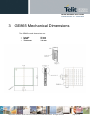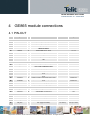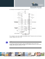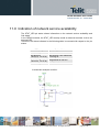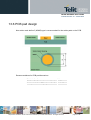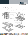
1
GE865 Hardware User Guide
1vv0300799 Rev.10 – 22-09-2009
GE865 Hardware User Guide
1vv0300799 Rev.10 – 22-09-2009
APPLICABILITY TABLE
PRODUCT
GE865
Reproduction forbidden without Telit Communications S.p.A. written authorization - All Rights Reserved
page 2 of 2
GE865 Hardware User Guide
1vv0300799 Rev.10 – 22-09-2009
DISCLAIMER
The information contained in this document is the proprietary information of Telit
Communications S.p.A. and its affiliates (“TELIT”). The contents are confidential and
any disclosure to persons other than the officers, employees, agents or subcontractors
of the owner or licensee of this document, without the prior written consent of Telit, is
strictly prohibited.
Telit makes every effort to ensure the quality of the information it makes available.
Notwithstanding the foregoing, Telit does not make any warranty as to the information
contained herein, and does not accept any liability for any injury, loss or damage of any
kind incurred by use of or reliance upon the information.
Telit disclaims any and all responsibility for the application of the devices characterized
in this document, and notes that the application of the device must comply with the
safety standards of the applicable country, and where applicable, with the relevant
wiring rules.
Telit reserves the right to make modifications, additions and deletions to this document
due to typographical errors, inaccurate information, or improvements to programs
and/or equipment at any time and without notice. Such changes will, nevertheless be
incorporated into new editions of this application note.
All rights reserved.
© 2009 Telit Communications S.p.A.
Reproduction forbidden without Telit Communications S.p.A. written authorization - All Rights Reserved
page 3 of 3
GE865 Hardware User Guide
1vv0300799 Rev.10 – 22-09-2009
Contents
APPLICABILITY TABLE ............................................................................................................................................................. 2
1
INTRODUCTION ......................................................................................................................................................... 6
1.1 SCOPE ................................................................................................................................................................................ 6
1.2 AUDIENCE ........................................................................................................................................................................... 6
1.3 CONTACT INFORMATION, SUPPORT .......................................................................................................................................... 6
1.4 DOCUMENT ORGANIZATION ................................................................................................................................................... 7
1.5 TEXT CONVENTIONS .............................................................................................................................................................. 8
1.6 RELATED DOCUMENTS........................................................................................................................................................... 8
1.7 DOCUMENT HISTORY ............................................................................................................................................................ 9
2
OVERVIEW .............................................................................................................................................................. 10
3
GE865 MECHANICAL DIMENSIONS .......................................................................................................................... 11
4
GE865 MODULE CONNECTIONS ............................................................................................................................... 12
4.1 PIN-OUT ......................................................................................................................................................................... 12
4.1.1 BGA Balls Layout .................................................................................................................................................... 15
5
HARDWARE COMMANDS ........................................................................................................................................ 16
5.1 TURNING ON THE GE865 ................................................................................................................................................... 16
5.2 TURNING OFF THE GE865 .................................................................................................................................................. 19
5.3 RESETTING THE GE865 ....................................................................................................................................................... 21
5.3.1 Hardware Unconditional restart ............................................................................................................................ 21
6
POWER SUPPLY ....................................................................................................................................................... 23
6.1 POWER SUPPLY REQUIREMENTS ............................................................................................................................................ 23
6.2 POWER CONSUMPTION ....................................................................................................................................................... 24
6.3 GENERAL DESIGN RULES ...................................................................................................................................................... 25
6.3.1 Electrical Design Guidelines ................................................................................................................................... 25
6.3.2 Thermal Design Guidelines ..................................................................................................................................... 29
6.3.3 Power Supply PCB layout Guidelines ...................................................................................................................... 30
7
ANTENNA ................................................................................................................................................................ 31
7.1 GSM ANTENNA REQUIREMENTS ........................................................................................................................................... 31
7.2 GSM ANTENNA - PCB LINE GUIDELINES ................................................................................................................................. 32
7.3 GSM ANTENNA - INSTALLATION GUIDELINES ........................................................................................................................... 33
8
LOGIC LEVEL SPECIFICATIONS .................................................................................................................................. 34
8.1 RESET SIGNAL .................................................................................................................................................................... 35
9
SERIAL PORTS .......................................................................................................................................................... 36
9.1 MODEM SERIAL PORT .................................................................................................................................................... 36
9.2 RS232 LEVEL TRANSLATION.................................................................................................................................................. 38
9.3 5V UART LEVEL TRANSLATION .............................................................................................................................................. 41
10
AUDIO SECTION OVERVIEW .................................................................................................................................... 43
10.1 ELECTRICAL CHARACTERISTICS ............................................................................................................................................. 44
10.1.1 Input Lines ............................................................................................................................................................ 44
Reproduction forbidden without Telit Communications S.p.A. written authorization - All Rights Reserved
page 4 of 4
GE865 Hardware User Guide
1vv0300799 Rev.10 – 22-09-2009
10.1.2 Output Lines ......................................................................................................................................................... 45
11
GENERAL PURPOSE I/O ........................................................................................................................................... 46
11.1 GPIO LOGIC LEVELS .......................................................................................................................................................... 47
11.2 USING A GPIO PAD AS INPUT ........................................................................................................................................... 48
11.3 USING A GPIO PAD AS OUTPUT ........................................................................................................................................ 48
11.4 USING THE RF TRANSMISSION CONTROL GPIO4 .................................................................................................................... 48
11.5 USING THE RFTXMON OUTPUT GPIO5 .............................................................................................................................. 48
11.6 USING THE ALARM OUTPUT GPIO6..................................................................................................................................... 49
11.7 USING THE BUZZER OUTPUT GPIO7 .................................................................................................................................... 49
11.8 MAGNETIC BUZZER CONCEPTS ............................................................................................................................................ 50
11.8.1 Short Description .................................................................................................................................................. 50
11.8.2 Frequency Behaviour ............................................................................................................................................ 51
11.8.3 Power Supply Influence ........................................................................................................................................ 51
11.8.4 Working Current Influence ................................................................................................................................... 51
11.9 INDICATION OF NETWORK SERVICE AVAILABILITY ..................................................................................................................... 52
11.10 RTC BYPASS OUT ........................................................................................................................................................... 53
11.11 EXTERNAL SIM HOLDER IMPLEMENTATION ......................................................................................................................... 53
12
DAC AND ADC SECTION ........................................................................................................................................... 54
12.1 DAC CONVERTER ............................................................................................................................................................. 54
12.1.1 Description ........................................................................................................................................................... 54
12.1.2 Enabling DAC ........................................................................................................................................................ 55
12.1.3 Low Pass Filter Example ....................................................................................................................................... 55
12.2 ADC CONVERTER ............................................................................................................................................................. 56
12.2.1 Description ........................................................................................................................................................... 56
12.2.2 Using ADC Converter ............................................................................................................................................ 56
13
MOUNTING THE GE865 ON YOUR BOARD ............................................................................................................... 57
13.1 GENERAL ........................................................................................................................................................................ 57
13.2 MODULE FINISHING & DIMENSIONS ..................................................................................................................................... 57
13.3 RECOMMENDED FOOT PRINT FOR THE APPLICATION ................................................................................................................. 58
13.4 DEBUG OF THE GE865 IN PRODUCTION ................................................................................................................................ 59
13.5 STENCIL .......................................................................................................................................................................... 59
13.6 PCB PAD DESIGN .............................................................................................................................................................. 60
13.7 SOLDER PASTE.................................................................................................................................................................. 61
13.7.1 GE865 Solder reflow ............................................................................................................................................. 62
14
PACKING SYSTEM .................................................................................................................................................... 64
14.1 MOISTURE SENSIBILITY....................................................................................................................................................... 65
15
CONFORMITY ASSESSMENT ISSUES ......................................................................................................................... 66
16
SAFETY RECOMMANDATIONS ................................................................................................................................. 68
Reproduction forbidden without Telit Communications S.p.A. written authorization - All Rights Reserved
page 5 of 5
GE865 Hardware User Guide
1vv0300799 Rev.10 – 22-09-2009
1 Introduction
1.1 Scope
The aim of this document is the description of some hardware solutions useful for developing a
product with the Telit GE865 module.
1.2 Audience
This document is intended for Telit customers, who are integrators, about to implement their
applications using our GE865 modules.
1.3 Contact Information, Support
For general contact, technical support, to report documentation errors and to order manuals,
contact Telit’s Technical Support Center (TTSC) at:
[email protected]
[email protected]
[email protected]
[email protected]
Alternatively, use:
http://www.telit.com/en/products/technical-support-center/contact.php
For detailed information about where you can buy the Telit modules or for recommendations on
accessories and components visit:
http://www.telit.com
To register for product news and announcements or for product questions contact Telit’s
Technical Support Center (TTSC).
Our aim is to make this guide as helpful as possible. Keep us informed of your comments and
suggestions for improvements.
Telit appreciates feedback from the users of our information.
Reproduction forbidden without Telit Communications S.p.A. written authorization - All Rights Reserved
page 6 of 6
GE865 Hardware User Guide
1vv0300799 Rev.10 – 22-09-2009
1.4 Document Organization
This document contains the following chapters:
Chapter 1: “Introduction” provides a scope for this document, target audience, contact and
support information, and text conventions.
Chapter 2: “Overview” provides an overview of the document.
Chapter 3: “GE865 Mechanical Dimensions”
Chapter 4: “GE865 Module Connections” deals with the pin out configuration and layout.
Chapter 5: “Hardware Commands” How to operate on the module via hardware.
Chapter 6: “Power supply” Power supply requirements and general design rules.
Chapter 7: “Antenna” The antenna connection and board layout design are the most important
parts in the full product design.
Chapter 8: “Logic Level specifications” Specific values adopted in the implementation of logic
levels for this module.
Chapter 9: “Serial ports” The serial port on the Telit GE865 is the core of the interface between
the module and OEM hardware
Chapter 10: “Audio Section overview” Refers to the audio blocks of the Base Band Chip of the
GE865 Telit Modules.
Chapter 11: “General Purpose I/O” How the general purpose I/O pads can be configured.
Chapter 12 “DAC and ADC Section” Deals with these two kind of converters.
Chapter 13: “Mounting the GE865 on the application board” Recommendations and specifics on
how to mount the module on the user’s board.
Reproduction forbidden without Telit Communications S.p.A. written authorization - All Rights Reserved
page 7 of 7
GE865 Hardware User Guide
1vv0300799 Rev.10 – 22-09-2009
1.5 Text Conventions
Danger – This information MUST be followed or catastrophic equipment failure or bodily
injury may occur.
Caution or Warning – Alerts the user to important points about integrating the module, if
these points are not followed, the module and end user equipment may fail or
malfunction.
Tip or Information – Provides advice and suggestions that may be useful when
integrating the module.
All dates are in ISO 8601 format, i.e. YYYY-MM-DD.
1.6 Related Documents
•
Telit's GSM/GPRS Family Software User Guide, 1vv0300784
•
Audio settings application note , 80000NT10007a
• Digital Voice Interface Application Note, 80000NT10004a
•
GE865 Product description,
•
SIM Holder Design Guides, 80000NT10001a
•
AT Commands Reference Guide, 80000ST10025a
•
Telit EVK2 User Guide, 1vv0300704
Reproduction forbidden without Telit Communications S.p.A. written authorization - All Rights Reserved
page 8 of 8
GE865 Hardware User Guide
1vv0300799 Rev.10 – 22-09-2009
1.7 Document History
Revision
Date
ISSUE#0
ISSUE#1
ISSUE#2
ISSUE#3
2009-01-26
2009-02-15
2009-02-15
2009-03-18
ISSUE#4
ISSUE#5
ISSUE#6
ISSUE#7
2009-04-02
03/06/2009
04/06/2009
2009-05-26
ISSUE#8
2009-06-18
ISSUE#9
2009-07-27
ISSUE#10
2009-09-22
Changes
First ISSUE# 0 - DRAFT
Updated current consumptions table
Updated Pinout description
Updated mechanical dimensions (balls spacing),
charger description removed,
Added better explanation of pin H5 (RF) and H1 (service)
Updated VBATT supply Range, DAC schematic, Conformity assessment
Updated section 13 (FCC Conformity assessment)
Updated section 13 (FCC Conformity assessment)
Applied new layout + minor editing
Edited PCB pad design par.13.1.6
Updated all schematic drawings
Updated Chapter 10 Audio Section
Substituted GE865-QUAD with GE865
Corrected GE864-QUAD/PY with GE865
Updated Overview section
Changed par. 5.1 Turning ON…. and par. 6.1 Power supply Requirements
Changed par. 13.3 and par.15 Conformity Assessment Issues
Added DVI pins description
Updated table of power consumptions.
Added note on chapters 5.1, 5.2, 9.3
Corrected chapter 1.1
Reproduction forbidden without Telit Communications S.p.A. written authorization - All Rights Reserved
page 9 of 9
GE865 Hardware User Guide
1vv0300799 Rev.10 – 22-09-2009
2 Overview
The aim of this document is the description of some hardware solutions useful for
developing a product with the Telit GE865 module.
In this document all the basic functions of a mobile phone will be taken into account; for
each one of them a proper hardware solution will be suggested and eventually the
wrong solutions and common errors to be avoided will be evidenced. Obviously this
document cannot embrace the whole hardware solutions and products that may be
designed. The wrong solutions to be avoided shall be considered as mandatory, while
the suggested hardware configurations shall not be considered mandatory, instead the
information given shall be used as a guide and a starting point for properly developing
your product with the Telit GE865 module. For further hardware details that may not be
explained in this document refer to the Telit GE865 Product Description document
where all the hardware information is reported.
NOTICE:
(EN) The integration of the GSM/GPRS GE865 cellular module within user application shall be
done according to the design rules described in this manual.
(IT) L’integrazione del modulo cellulare GSM/GPRS GE865 all’interno dell’applicazione
dell’utente dovrà rispettare le indicazioni progettuali descritte in questo manuale.
(DE) Die Integration des GE865 GSM/GPRS Mobilfunk-Moduls in ein Gerät muß gemäß der in
diesem Dokument beschriebenen Kunstruktionsregeln erfolgen.
(SL) Integracija GSM/GPRS GE865 modula v uporabniški aplikaciji bo morala upoštevati
projektna navodila, opisana v tem piročniku.
(SP) La utilización del modulo GSM/GPRS GE865 debe ser conforme a los usos para los cuales
ha sido deseñado descritos en este manual del usuario.
(FR) L’intégration du module cellulaire GSM/GPRS GE865 dans l’application de l’utilisateur sera
faite selon les règles de conception décrites dans ce manuel.
(HE)
GE865-QUAD
The information presented in this document is believed to be accurate and reliable.
However, no responsibility is assumed by Telit Communications S.p.A. for its use, nor
any infringement of patents or other rights of third parties which may result from its use.
No license is granted by implication or otherwise under any patent rights of Telit
Communications S.p.A. other than for circuitry embodied in Telit products. This
document is subject to change without notice.
Reproduction forbidden without Telit Communications S.p.A. written authorization - All Rights Reserved
page 10 of 10
GE865 Hardware User Guide
1vv0300799 Rev.10 – 22-09-2009
3 GE865 Mechanical Dimensions
The GE865 overall dimensions are:
•
•
•
Length:
Width:
Thickness:
22 mm
22 mm
3.0 mm
Reproduction forbidden without Telit Communications S.p.A. written authorization - All Rights Reserved
page 11 of 11
GE865 Hardware User Guide
1vv0300799 Rev.10 – 22-09-2009
4 GE865 module connections
4.1 PIN-OUT
Ball
Signal
I/O
Function
Note
Type
E8
EAR-
AO
Earphone signal output, phase -
Audio
D8
EAR+
AO
Earphone signal output, phase +
Audio
B8
MIC+
AI
Mic.signal input; phase+
Audio
C8
MIC-
AI
Mic.signal input; phase-
Audio
Audio
SIM card interface
A5
SIMCLK
O
External SIM signal – Clock
A8
SIMRST
O
External SIM signal – Reset
A6
SIMIO
I/O
External SIM signal – Data I/O
B7
SIMIN
I
1,8 / 3V
A7
SIMVCC
-
External SIM signal – Presence (active low)
External SIM signal – Power supply for the
SIM
Trace
D1
TXD_AUX
O
Auxiliary UART (TX Data)
CMOS 2.8V
E1
RXD_AUX
I
Auxiliary UART (RX Data)
CMOS 2.8V
A3
C103/TXD
I
Serial data input (TXD) from DTE
CMOS 2.8V
A4
C104/RXD
O
CMOS 2.8V
B3
C108/DTR
I
A1
C105/RTS
I
A2
C106/CTS
O
B5
C109/DCD
O
B2
C107/DSR
O
Serial data output to DTE
Input for Data terminal ready signal (DTR) from
DTE
Input for Request to send signal (RTS) from
DTE
Output for Clear to send signal (CTS) to DTE
Output for Data carrier detect signal (DCD) to
DTE
Output for Data set ready signal (DSR) to DTE
B4
C125/RING
O
Output for Ring indicator signal (RI) to DTE
CMOS 2.8V
G7
DAC_OUT
AO
Digital/Analog converter output
D/A
F5
ADC_IN1
AI
Analog/Digital converter input
A/D
F6
ADC_IN2
AI
Analog/Digital converter input
A/D
1,8 / 3V
1,8 / 3V
4.7K Pull up
1,8 / 3V
1,8 / 3V
Prog. / Data + HW Flow Control
CMOS 2.8V
CMOS 2.8V
CMOS 2.8V
CMOS 2.8V
CMOS 2.8V
DAC and ADC
Miscellaneous Functions
C1
RESET*
I
Reset input
H2
VRTC
AO
VRTC Backup capacitor
Power
G8
STAT_LED
O
Status indicator led
CMOS 1.8V
B1
ON_OFF*
I
Input command for switching power ON or
OFF (toggle command).
47K Pull Up
Reproduction forbidden without Telit Communications S.p.A. written authorization - All Rights Reserved
Pull up to VRTC
page 12 of 12
GE865 Hardware User Guide
1vv0300799 Rev.10 – 22-09-2009
Ball
Signal
I/O
Function
Note
Type
E2
PWRMON
O
Power ON Monitor
CMOS 2.8V
H5
Antenna
O
RF
H1
Service
I
D3
GPIO_01 / DVI_WA0
I/O
D2
GPIO_02 / JDR /
DVI_RX
I/O
E4
GPIO_03 / DVI_TX
I/O
H7
GPIO_04 / TX_DISAB
I/O
G2
GPIO_05 / RFTXMON
I/O
Antenna output – 50 Ω
Service pin shall be used to upgrade the
module from ASC1 (RXD AUX, TXD_AUX).
The pin shall be tied low to enable the feature
only in case of a SW Update activity. It is
required, for debug purpose, to be connected
to a test pad on the final application.
GPIO
GPIO01 Configurable GPIO / Digital Audio
Interface (WA0)
GPIO02 I/O pin / Jammer Detect Report /
Digital Audio Interface (RX)
GPIO03 GPIO I/O pin // Digital Audio Interface
(TX)
GPIO04 Configurable GPIO / TX Disable input
GPIO05 Configurable GPIO / Transmitter ON
monitor
GPIO06 Configurable GPIO / ALARM
H8
GPIO_06 / ALARM
I/O
G6
GPIO_07 / BUZZER
I/O
D4
GPIO_08 / DVI_CLK
I/O
F4
GPIO_09
I/O
E3
GPIO_10
I/O
CMOS 2.8V
CMOS 2.8V
CMOS 2.8V
CMOS 2.8V
CMOS 2.8V
CMOS 2.8V
CMOS 2.8V
GPIO07 Configurable GPIO / Buzzer
GPIO08 Configurable GPIO / Digital Audio
Interface (CLK)
GPIO09
CMOS 2.8V
4.7 K Pull Up
Open Drain
GPIO10
4.7 K Pull Up
Open Drain
CMOS 2.8V
Power Supply
F1
VBATT
-
Main power supply (Baseband)
Power
F2
VBATT_PA
-
Main power supply (Radio PA)
Power
F3
VBATT_PA
-
Main power supply (Radio PA)
Power
G1
GND
-
Ground
Power
C2
GND
-
Ground
Power
C7
GND
-
Ground
Power
E5
GND
-
Ground
Power
E7
GND
-
Ground
Power
G5
GND
-
Ground
Power
G4
GND
-
Ground
Power
G3
GND
-
Ground
Power
H3
GND
-
Ground
Power
H6
GND
-
Ground
Power
RESERVED
B6
-
C3
-
C4
-
C5
-
C6
-
D5
-
D6
-
D7
-
E6
-
Reproduction forbidden without Telit Communications S.p.A. written authorization - All Rights Reserved
page 13 of 13
GE865 Hardware User Guide
1vv0300799 Rev.10 – 22-09-2009
Ball
Signal
I/O
F7
-
F8
-
Function
Note
Type
WARNING:
Reserved pins must not be connected.
NOTE:
If not used, almost all pins should be left disconnected. The only exceptions are the
following pins:
pin
F1,F2,F3
G1, C2, C7, E5, E7, G5,
G4, G3, H3, H6
signal
VBATT & VBATT_PA
B1
A3
C1
A4
A1
D1
E1
H1
ON/OFF*
TXD
RESET*
RXD
1
RTS
TXD_AUX
RXD_AUX
Service
GND
Reproduction forbidden without Telit Communications S.p.A. written authorization - All Rights Reserved
page 14 of 14
GE865 Hardware User Guide
1vv0300799 Rev.10 – 22-09-2009
4.1.1 BGA Balls Layout
TOP VIEW
A
B
C
D
E
F
G
H
1
C105 /
RTS
ON_OFF
RESET*
TXD_AUX
RXD_AUX
VBATT
GND
SERVICE
2
C106/CTS
C107/DSR
GND
GPIO_02 /
DVI_RX
PWRMON
VBATT_P
A
GPIO_05
VRTC
3
C103_TXD
C108/DTR
-
GPIO_01 /
DVI_WA0
GPIO_10
VBATT_P
A
GND
GND
4
C104/RXD
C125/RING
-
GPIO_08 /
DVI_CLK
GPIO_03 /
DVI_TX
GPIO_09
GND
5
SIMCLK
C109/DCD
-
-
GND
ADC1
GND
ANT
6
SIMIO
-
-
-
-
ADC2
GPIO_07
GND
7
SIMVCC
SIMIN
GND
-
GND
-
DAC
GPIO_04
8
SIMRST
MIC+
MIC-
EAR+
EAR-
-
STATLED
GPIO_06
LEGENDA:
AUDIO
SIM CARD
ANTENNA
UARTS
DAC and ADC
MISCELLANEOUS
GPIO
POWER SUPPLY VBATT
POWER SUPPLY GND
RESERVED
NOTE:
The pin defined as H4 has to be considered RESERVED and not connected on any pin
in the application. The related area on the application has to be kept empty.
Reproduction forbidden without Telit Communications S.p.A. written authorization - All Rights Reserved
page 15 of 15
GE865 Hardware User Guide
1vv0300799 Rev.10 – 22-09-2009
5 Hardware Commands
5.1 Turning ON the GE865
To turn on the GE865 the pad ON# must be tied low for at least 1 second and then
released.
When the power supply voltage is lower than 3.4V the pad ON# must be tied low at
least 3 seconds.
The maximum current that can be drained from the ON# pad is 0,1 mA.
A simple circuit to do it is:
ON#
R1
Q1
Power ON impulse
R2
GND
NOTE:
Don't use any pull up resistor on the ON# line, it is internally pulled up. Using pull up
resistor may bring to latch up problems on the GE865 power regulator and improper
power on/off of the module. The line ON# must be connected only in open collector
configuration.
Reproduction forbidden without Telit Communications S.p.A. written authorization - All Rights Reserved
page 16 of 16
GE865 Hardware User Guide
1vv0300799 Rev.10 – 22-09-2009
NOTE:
In this document all the lines that are inverted, hence have active low signals are
labelled with a name that ends with”#" or with a bar over the name.
TIP:
To check if the device has powered on, the hardware line PWRMON should be
monitored. After 900ms the line raised up the device could be considered powered on.
NOTE:
It is mandatory to avoid sending data to the serial ports during the first 200mS of the
module startup.
NOTE:
It is recommended to avoid having any HIGH logic level signal applied to the digital pins
of the GE865 when the module is powered off.
Reproduction forbidden without Telit Communications S.p.A. written authorization - All Rights Reserved
page 17 of 17
GE865 Hardware User Guide
1vv0300799 Rev.10 – 22-09-2009
A flow chart showing the proper turn on procedure is displayed below:
Reproduction forbidden without Telit Communications S.p.A. written authorization - All Rights Reserved
page 18 of 18
GE865 Hardware User Guide
1vv0300799 Rev.10 – 22-09-2009
For example:
1- Let's assume you need to drive the ON# pad with a totem pole output of a +3/5 V
microcontroller (uP_OUT1):
2- Let's assume you need to drive the ON# pad directly with an ON/OFF button:
5.2 Turning OFF the GE865
Turning off of the device can be done in two ways:
•
via AT command (see GE865 Software User Guide, AT#SHDN)
•
by tying low pin ON#
Either ways, the device issues a detach request to network informing that the device will not be
reachable any more.
To turn OFF the GE865 the pad ON# must be tied low for at least 2 seconds and then released. A
Pulse duration less than 2 seconds should also start the power off procedure, but this is not
guaranteed.
Reproduction forbidden without Telit Communications S.p.A. written authorization - All Rights Reserved
page 19 of 19
GE865 Hardware User Guide
1vv0300799 Rev.10 – 22-09-2009
The same circuitry and timing for the power on must be used.
The device shuts down after the release of the ON# pad.
The following flow chart shows the proper turnoff procedure:
TIP:
To check if the device has been powered off, the hardware line PWRMON must be
monitored. The device is powered off when PWRMON goes low.
It is recommended to avoid having HIGH logic levels applied to the digital pins during
the ON/OFF transitions and when the module is switched off.
Reproduction forbidden without Telit Communications S.p.A. written authorization - All Rights Reserved
page 20 of 20
GE865 Hardware User Guide
1vv0300799 Rev.10 – 22-09-2009
5.3 Resetting the GE865
5.3.1 Hardware Unconditional restart
WARNING:
The hardware unconditional Restart must not be used during normal operation of the
device since it does not detach the device from the network. It shall be kept as an
emergency exit procedure to be done in the rare case that the device gets stacked
waiting for some network or SIM responses.
To unconditionally reboot the GE865, the pad RESET# must be tied low for at least 200 milliseconds
and then released.
The maximum current that can be drained from the ON# pad is 0,15 mA.
NOTE:
Do not use any pull up resistor on the RESET* line nor any totem pole digital output.
Using pull up resistor may bring to latch up problems on the GE865 power regulator
and improper functioning of the module. The line RESET* must be connected only in
open collector configuration.
TIP:
The unconditional hardware restart must always be implemented on the boards and the
software must use it as an emergency exit procedure.
A simple circuit to do it is:
Reproduction forbidden without Telit Communications S.p.A. written authorization - All Rights Reserved
page 21 of 21
GE865 Hardware User Guide
1vv0300799 Rev.10 – 22-09-2009
In the following flow chart is detailed the proper restart procedure:
For example:
1- Let us assume you need to drive the RESET# pad with a totem pole output of a
+3/5 V microcontroller (uP_OUT2):
Reproduction forbidden without Telit Communications S.p.A. written authorization - All Rights Reserved
page 22 of 22
GE865 Hardware User Guide
1vv0300799 Rev.10 – 22-09-2009
6 Power Supply
The power supply circuitry and board layout are a very important part in the full product
design and they strongly reflect on the product overall performances, hence read
carefully the requirements and the guidelines that will follow for a proper design.
6.1 Power Supply Requirements
The external power supply must be connected to VBATT & VBATT_PA signals and
must fulfill the following requirements:
POWER SUPPLY
Nominal Supply Voltage
Normal Operating Voltage Range
Extended Operating Voltage Range
3.8 V
3.4 V÷ 4.20 V
3.22 V÷ 4.50 V
NOTE:
The Operating Voltage Range MUST never be exceeded; care must be taken in order
to fulfil min/max voltage requirement.
NOTE:
Overshoot voltage (regarding MAX Extended Operating Voltage) and drop in voltage
(regarding MIN Extended Operating Voltage) MUST never be exceeded;
The “Extended Operating Voltage Range” can be used only with completely
assumption and application of the HW User guide suggestions.
NOTE:
When the power supply voltage is lower than 3.4V, to turn ON the module, the pad
ON# must be tied low for at least 3 seconds. See para 5.1.
Reproduction forbidden without Telit Communications S.p.A. written authorization - All Rights Reserved
page 23 of 23
GE865 Hardware User Guide
1vv0300799 Rev.10 – 22-09-2009
6.2 Power Consumption
The GE865 power consumptions are:
GE865
Average
Mode
(mA)
SWITCHED OFF
Switched Off
<62uA
AT+CFUN=1
AT+CFUN=4
19,0
18,0
3,9
2,9
AT+CFUN=0 or =5
2,1
1,9
1,6
CSD TX and RX mode
GSM900 CSD PL5
305,0
DCS1800 CSD PL0
208,0
GPRS (class 10) 1TX
GSM900 PL5
264,0
DCS1800 PL0
176,0
GPRS (class 10) 2TX
GSM900 PL5
473,8
DCS1800 PL0
307,8
Mode description
Module supplied but Switched Off
IDLE mode
Normal mode: full functionality of the module
Disabled TX and RX; module is not registered on the network
Paging Multiframe 2
Paging Multiframe 4
Paging Multiframe 6
Paging Multiframe 8
Paging Multiframe 9
GSM VOICE CALL
GPRS Sending data mode
GPRS Sending data mode
The GSM system is made in a way that the RF transmission is not continuous, else it is
packed into bursts at a base frequency of about 216 Hz, and the relative current peaks
can be as high as about 2A. Therefore the power supply has to be designed in order to
withstand with these current peaks without big voltage drops; this means that both the
electrical design and the board layout must be designed for this current flow.
If the layout of the PCB is not well designed a strong noise floor is generated on the
ground and the supply; this will reflect on all the audio paths producing an audible
annoying noise at 216 Hz; if the voltage drop during the peak current absorption is too
much, then the device may even shutdown as a consequence of the supply voltage
drop.
NOTE:
The electrical design for the Power supply should be made ensuring it will be capable
of a peak current output of at least 2 A.
Reproduction forbidden without Telit Communications S.p.A. written authorization - All Rights Reserved
page 24 of 24
GE865 Hardware User Guide
1vv0300799 Rev.10 – 22-09-2009
6.3 General Design Rules
The principal guidelines for the Power Supply Design embrace three different design
steps:
• the electrical design
• the thermal design
• the PCB layout.
6.3.1 Electrical Design Guidelines
•
•
•
The electrical design of the power supply depends strongly from the power source
where this power is drained. We will distinguish them into three categories:
+5V input (typically PC internal regulator output)
+12V input (typically automotive)
Battery
6.3.1.1 + 5V input Source Power Supply Design Guidelines
•
•
•
•
•
The desired output for the power supply is 3.8V, hence there's not a big difference
between the input source and the desired output and a linear regulator can be used. A
switching power supply will not be suited because of the low drop out requirements.
When using a linear regulator, a proper heat sink shall be provided in order to dissipate
the power generated.
A Bypass low ESR capacitor of adequate capacity must be provided in order to cut the
current absorption peaks close to the GE865, a 100µF tantalum capacitor is usually
suited.
Make sure the low ESR capacitor on the power supply output (usually a tantalum one)
is rated at least 10V.
A protection diode should be inserted close to the power input, in order to save the
GE865 from power polarity inversion.
Reproduction forbidden without Telit Communications S.p.A. written authorization - All Rights Reserved
page 25 of 25
GE865 Hardware User Guide
1vv0300799 Rev.10 – 22-09-2009
An example of linear regulator with 5V input is:
6.3.1.2 + 12V input Source Power Supply Design Guidelines
•
•
•
•
•
•
•
•
The desired output for the power supply is 3.8V, hence due to the big difference
between the input source and the desired output, a linear regulator is not suited and
shall not be used. A switching power supply will be preferable because of its better
efficiency especially with the 2A peak current load represented by the GE865.
When using a switching regulator, a 500kHz or more switching frequency regulator is
preferable because of its smaller inductor size and its faster transient response. This
allows the regulator to respond quickly to the current peaks absorption.
In any case the frequency and Switching design selection is related to the application to
be developed due to the fact the switching frequency could also generate EMC
interferences.
For car PB battery the input voltage can rise up to 15,8V and this should be kept in
mind when choosing components: all components in the power supply must withstand
this voltage.
A Bypass low ESR capacitor of adequate capacity must be provided in order to cut the
current absorption peaks, a 100µF tantalum capacitor is usually suited.
Make sure the low ESR capacitor on the power supply output (usually a tantalum one)
is rated at least 10V.
For Car applications a spike protection diode should be inserted close to the power
input, in order to clean the supply from spikes.
A protection diode should be inserted close to the power input, in order to save the
GE865 from power polarity inversion. This can be the same diode as for spike
protection.
Reproduction forbidden without Telit Communications S.p.A. written authorization - All Rights Reserved
page 26 of 26
GE865 Hardware User Guide
1vv0300799 Rev.10 – 22-09-2009
An example of switching regulator with 12V input is in the below schematic (split in 2
parts):
6.3.1.3 Battery Source Power Supply Design Guidelines
•
The desired nominal output for the power supply is 3.8V and the maximum voltage
allowed is 4.2V, hence a single 3.7V Li-Ion cell battery type is suited for supplying the
power to the Telit GE865 module.
Reproduction forbidden without Telit Communications S.p.A. written authorization - All Rights Reserved
page 27 of 27
GE865 Hardware User Guide
1vv0300799 Rev.10 – 22-09-2009
WARNING:
The three cells Ni/Cd or Ni/MH 3,6 V Nom. battery types or 4V PB types MUST NOT
BE USED DIRECTLY since their maximum voltage can rise over the absolute
maximum voltage for the GE865 and damage it.
NOTE:
DON'T USE any Ni-Cd, Ni-MH, and Pb battery types directly connected with GE865.
Their use can lead to overvoltage on the GE865 and damage it. USE ONLY Li-Ion
battery types.
•
•
•
•
A Bypass low ESR capacitor of adequate capacity must be provided in order to cut the
current absorption peaks, a 100µF tantalum capacitor is usually suited.
Make sure the low ESR capacitor (usually a tantalum one) is rated at least 10V.
A protection diode should be inserted close to the power input, in order to save the
GE865 from power polarity inversion. Otherwise the battery connector should be done
in a way to avoid polarity inversions when connecting the battery.
The battery capacity must be at least 500mAh in order to withstand the current peaks of
2A; the suggested capacity is from 500mAh to 1000mAh.
Reproduction forbidden without Telit Communications S.p.A. written authorization - All Rights Reserved
page 28 of 28
GE865 Hardware User Guide
1vv0300799 Rev.10 – 22-09-2009
6.3.2 Thermal Design Guidelines
•
•
•
•
The thermal design for the power supply heat sink should be done with the following
specifications:
Average current consumption during transmission @ max PWR level:
500mA
Average current consumption during transmission @ min PWR level:
100mA
Average current during Power Saving (CFUN=5) :
2,4mA
Average current during idle (Power Saving disabled):
24mA
NOTE:
The average consumption during transmissions depends on the power level at which
the device is requested to transmit by the network. The average current consumption
hence varies significantly.
Considering the very low current during idle, especially if Power Saving function is
enabled, it is possible to consider from the thermal point of view that the device absorbs
current significantly only during calls.
If we assume that the device stays into transmission for short periods of time (let's say
few minutes) and then remains for a quite long time in idle (let's say one hour), then the
power supply has always the time to cool down between the calls and the heat sink
could be smaller than the calculated one for 500mA maximum RMS current, or even
could be the simple chip package (no heat sink).
Moreover in the average network conditions the device is requested to transmit at a
lower power level than the maximum and hence the current consumption will be less
than the 500mA, being usually around 150mA.
For these reasons the thermal design is rarely a concern and the simple ground plane
where the power supply chip is placed can be enough to ensure a good thermal
condition and avoid overheating.
For the heat generated by the GE865, you can consider it to be during transmission 1W
max during CSD/VOICE calls and 2W max during class10 GPRS upload.
This generated heat will be mostly conducted to the ground plane under the GE865;
you must ensure that your application can dissipate it.
Reproduction forbidden without Telit Communications S.p.A. written authorization - All Rights Reserved
page 29 of 29
GE865 Hardware User Guide
1vv0300799 Rev.10 – 22-09-2009
6.3.3 Power Supply PCB layout Guidelines
As seen on the electrical design guidelines the power supply shall have a low ESR
capacitor on the output to cut the current peaks and a protection diode on the input to
protect the supply from spikes and polarity inversion. The placement of these
components is crucial for the correct working of the circuitry. A misplaced component
can be useless or can even decrease the power supply performances.
•
•
•
•
•
•
•
•
The Bypass low ESR capacitor must be placed close to the Telit GE865 power input
pads or in the case the power supply is a switching type it can be placed close to the
inductor to cut the ripple provided the PCB trace from the capacitor to the GE865 is
wide enough to ensure a dropless connection even during the 2A current peaks.
The protection diode must be placed close to the input connector where the power
source is drained.
The PCB traces from the input connector to the power regulator IC must be wide
enough to ensure no voltage drops occur when the 2A current peaks are absorbed.
Note that this is not made in order to save power loss but especially to avoid the
voltage drops on the power line at the current peaks frequency of 216 Hz that will
reflect on all the components connected to that supply, introducing the noise floor at the
burst base frequency. For this reason while a voltage drop of 300-400 mV may be
acceptable from the power loss point of view, the same voltage drop may not be
acceptable from the noise point of view. If your application doesn't have audio interface
but only uses the data feature of the Telit GE865, then this noise is not so disturbing
and power supply layout design can be more forgiving.
The PCB traces to the GE865 and the Bypass capacitor must be wide enough to
ensure no significant voltage drops occur when the 2A current peaks are absorbed.
This is for the same reason as previous point. Try to keep this trace as short as
possible.
The PCB traces connecting the Switching output to the inductor and the switching
diode must be kept as short as possible by placing the inductor and the diode very
close to the power switching IC (only for switching power supply). This is done in order
to reduce the radiated field (noise) at the switching frequency (100-500 kHz usually).
The use of a good common ground plane is suggested.
The placement of the power supply on the board should be done in such a way to
guarantee that the high current return paths in the ground plane are not overlapped to
any noise sensitive circuitry as the microphone amplifier/buffer or earphone amplifier.
The power supply input cables should be kept separate from noise sensitive lines such
as microphone/earphone cables.
Reproduction forbidden without Telit Communications S.p.A. written authorization - All Rights Reserved
page 30 of 30
GE865 Hardware User Guide
1vv0300799 Rev.10 – 22-09-2009
7 Antenna
The antenna connection and board layout design are the most important part in the full
product design and they strongly reflect on the product overall performances, hence
read carefully and follow the requirements and the guidelines for a proper design.
7.1 GSM Antenna Requirements
As suggested on the Product Description the antenna and antenna line on PCB for a
Telit GE865 device shall fulfil the following requirements:
ANTENNA REQUIREMENTS
Depending by frequency band(s) provided by
the network operator, the customer shall use
Frequency range
the most suitable antenna for that/those
band(s)
70 MHz in GSM850, 80 MHz in GSM900,
Bandwidth
170 MHz in DCS & 140 MHz PCS band
Gain
Gain < 3dBi
Impedance
50Ω
Input power
> 2 W peak power
VSWR absolute max
≤ 10:1
VSWR recommended ≤ 2:1
When using the GE865, since there's no antenna connector on the module, the
antenna must be connected to the GE865 through the PCB with the antenna pad (BGA
Ball H5).
In the case that the antenna is not directly developed on the same PCB, hence directly
connected at the antenna pad of the GE865, then a PCB line is needed in order to
connect with it or with its connector.
Reproduction forbidden without Telit Communications S.p.A. written authorization - All Rights Reserved
page 31 of 31
GE865 Hardware User Guide
1vv0300799 Rev.10 – 22-09-2009
This line of transmission shall fulfill the following requirements:
ANTENNA LINE ON PCB REQUIREMENTS
Impedance
50Ω
Max Attenuation
0,3 dB
No coupling with other signals allowed
Cold End (Ground Plane) of antenna shall be
equipotential to the GE865 ground pins
Furthermore if the device is developed for the US market and/or Canada market, it shall
comply with the FCC and/or IC approval requirements:
This device is to be used only for mobile and fixed application. In order to re-use the
Telit FCC/IC approvals the antenna(s) used for this transmitter must be installed to
provide a separation distance of at least 20 cm from all persons and must not be colocated or operating in conjunction with any other antenna or transmitter. If antenna is
installed with a separation distance of less than 20 cm from all persons or is co-located
or operating in conjunction with any other antenna or transmitter then additional FCC/IC
testing may be required. End-Users must be provided with transmitter operation
conditions for satisfying RF exposure compliance.
Antennas used for this OEM module must not exceed 3dBi gain for mobile and fixed
operating configurations.
7.2 GSM Antenna - PCB line Guidelines
•
•
•
•
•
•
•
•
•
•
Ensure that the antenna line impedance is 50Ω ;
Keep the antenna line on the PCB as short as possible, since the antenna line loss
shall be less than 0,3 dB;
Antenna line must have uniform characteristics, constant cross section, avoid
meanders and abrupt curves;
Keep, if possible, one layer of the PCB used only for the Ground plane;
Surround (on the sides, over and under) the antenna line on PCB with Ground, avoid
having other signal tracks facing directly the antenna line track;
The ground around the antenna line on PCB has to be strictly connected to the Ground
Plane by placing vias once per 2mm at least;
Place EM noisy devices as far as possible from GE865 antenna line;
Keep the antenna line far away from the GE865 power supply lines;
If you have EM noisy devices around the PCB hosting the GE865, such as fast
switching ICs, take care of the shielding of the antenna line by burying it inside the
layers of PCB and surround it with Ground planes, or shield it with a metal frame cover.
If you don't have EM noisy devices around the PCB of GE865, by using a strip-line on
the superficial copper layer for the antenna line, the line attenuation will be lower than a
buried one;
Reproduction forbidden without Telit Communications S.p.A. written authorization - All Rights Reserved
page 32 of 32
GE865 Hardware User Guide
1vv0300799 Rev.10 – 22-09-2009
7.3 GSM Antenna - Installation Guidelines
•
•
•
•
•
Install the antenna in a place covered by the GSM signal.
If the device antenna is located greater then 20cm from the human body and there are
no co-located transmitter then the Telit FCC/IC approvals can be re-used by the end
product
If the device antenna is located less then 20cm from the human body or there are no
co-located transmitter then the additional FCC/IC testing may be required for the end
product (Telit FCC/IC approvals cannot be reused)
Antenna shall not be installed inside metal cases
Antenna shall be installed also according Antenna manufacturer instructions.
Reproduction forbidden without Telit Communications S.p.A. written authorization - All Rights Reserved
page 33 of 33
GE865 Hardware User Guide
1vv0300799 Rev.10 – 22-09-2009
8 Logic level specifications
Where not specifically stated, all the interface circuits work at 2.8V CMOS logic levels.
The following table shows the logic level specifications used in the GE865 interface
circuits:
Absolute Maximum Ratings -Not Functional
Parameter
Min
Max
Input level on any digital pin
(CMOS 2.8) when on
Input level on any digital pin
(CMOS 1.8) when on
Input voltage on analog pins
when on
-0.3V
+3.1V
-0.3V
+2.1V
-0.3V +3.0 V
Operating Range - Interface levels (2.8V CMOS)
Level
Min
Max
Input high level
Input low level
Output high level
Output low level
2.1V
3.0V
0V
2.2V
0V
0.5V
3.0V
0.35V
For 1.8V signals:
Operating Range - Interface levels (1.8V CMOS)
Level
Min
Max
Input high level
Input low level
Output high level
Output low level
1.6V
2.0V
0V
1,65V
0V
0.4V
2.0V
0.35V
Current characteristics
Level
Typical
Output Current
1mA
Input Current
1uA
Reproduction forbidden without Telit Communications S.p.A. written authorization - All Rights Reserved
page 34 of 34
GE865 Hardware User Guide
1vv0300799 Rev.10 – 22-09-2009
8.1 Reset signal
Signal
RESET#
Function
Phone reset
I/O
I
Bga Ball
C1
RESET# is used to reset the GE865 . Whenever this signal is pulled low, the GE865 is
reset. When the device is reset it stops any operation. After the release of the reset
GE865 is unconditionally shut down, without doing any detach operation from the
network where it is registered. This behaviour is not a proper shut down because any
GSM device is requested to issue a detach request on turn off. For this reason the
Reset signal must not be used to normally shutting down the device, but only as an
emergency exit in the rare case the device remains stuck waiting for some network
response.
The RESET# is internally controlled on start-up to achieve always a proper power-on
reset sequence, so there's no need to control this pin on start-up. It may only be used
to reset a device already on that is not responding to any command.
NOTE:
Do not use this signal to power off the GE865. Use the ON/OFF signal to perform this
function or the AT#SHDN command.
Reset Signal Operating levels:
Signal
RESET Input high
RESET Input low
Min
1.8V*
0V
Max
2.1V
0.2V
* this signal is internally pulled up so the pin can be left floating if not used.
If unused, this signal may be left unconnected. If used, then it must always be
connected with an open collector transistor, to permit to the internal circuitry the
power on reset and under voltage lockout functions.
Reproduction forbidden without Telit Communications S.p.A. written authorization - All Rights Reserved
page 35 of 35
GE865 Hardware User Guide
1vv0300799 Rev.10 – 22-09-2009
9 Serial Ports
The serial port on the GE865 is the core of the interface between the module and OEM
hardware.
2 serial ports are available on the module:
• MODEM SERIAL PORT 1 (MAIN)
• MODEM SERIAL PORT 2 (AUX)
9.1 MODEM SERIAL PORT
Several configurations can be designed for the serial port on the OEM hardware, but
the most common are:
• RS232 PC com port
• microcontroller UART @ 2.8V - 3V (Universal Asynchronous Receive Transmit)
• microcontroller UART @ 5V or other voltages different from 2.8V
Depending from the type of serial port on the OEM hardware a level translator circuit
may be needed to make the system work. The only configuration that doesn't need a
level translation is the 2.8V UART.
The serial port on the GE865 is a +2.8V UART with all the 7 RS232 signals. It differs
from the PC-RS232 in the signal polarity (RS232 is reversed) and levels. The levels for
the GE865 UART are the CMOS levels:
Absolute Maximum Ratings -Not Functional
Parameter
Min
Max
Input level on any
digital pad when on
Input voltage on
analog pads when on
-0.3V
+3.1V
-0.3V
+3.1V
Operating Range - Interface levels (2.8V CMOS)
Level
Min
Max
Input high level
VIH
2.1V
3.0 V
Input low level
VIL
0V
0.5V
Output high level VOH
2.2V
3.0V
Output low level VOL
0V
0.35V
Reproduction forbidden without Telit Communications S.p.A. written authorization - All Rights Reserved
page 36 of 36
GE865 Hardware User Guide
1vv0300799 Rev.10 – 22-09-2009
The signals of the GE865 serial port are:
RS232
Pin
Number
Signal
GE865
Pad
Number
Name
1
DCD - dcd_uart
B5
Data Carrier Detect
Output from the GE865 that indicates
the carrier presence
A4
Transmit line *see Note
Output transmit line of GE865 UART
A3
Receive line *see Note
Input receive of the GE865 UART
DTR - dtr_uart
B3
Data Terminal Ready
5
GND
C2, C7, E5,
E7, G1, G3,
G4, G5, H3,
H6
Ground
6
DSR - dsr_uart
B2
Data Set Ready
7
RTS -rts_uart
A1
Request to Send
8
CTS - cts_uart
A2
Clear to Send
9
RI - ri_uart
B4
Ring Indicator
2
3
4
RXD tx_uart
TXD rx_uart
Usage
Input to the GE865 that controls the
DTE READY condition
ground
Output from the GE865 that indicates
the module is ready
Input to the GE865 that controls the
Hardware flow control
Output from the GE865 that controls
the Hardware flow control
Output from the GE865 that indicates
the incoming call condition
NOTE:
According to V.24, RX/TX signal names are referred to the application side, therefore
on the GE865 side these signal are on the opposite direction: TXD on the application
side will be connected to the receive line (here named TXD/ rx_uart ) of the GE865
serial port and viceversa for RX.
NOTE:
For a minimum implementation, only the TXD and RXD lines can be connected, the
other lines can be left open provided a software flow control is implemented.
Reproduction forbidden without Telit Communications S.p.A. written authorization - All Rights Reserved
page 37 of 37
GE865 Hardware User Guide
1vv0300799 Rev.10 – 22-09-2009
9.2 RS232 level translation
In order to interface the GE865 with a PC com port or a RS232 (EIA/TIA-232)
application a level translator is required. This level translator must:
•
invert the electrical signal in both directions;
•
change the level from 0/2.8V to +15/-15V .
Actually, the RS232 UART 16450, 16550, 16650 & 16750 chipsets accept signals with
lower levels on the RS232 side (EIA/TIA-562), allowing a lower voltage-multiplying ratio
on the level translator. Note that the negative signal voltage must be less than 0V and
hence some sort of level translation is always required.
The simplest way to translate the levels and invert the signal is by using a single chip
level translator. There are a multitude of them, differing in the number of drivers and
receivers and in the levels (be sure to get a true RS232 level translator not a RS485 or
other standards).
By convention the driver is the level translator from the 0-2.8V UART to the RS232
level. The receiver is the translator from the RS232 level to 0-2.8V UART.
In order to translate the whole set of control lines of the UART you will need:
• 5 drivers
• 3 receivers
NOTE:
The digital input lines working at 2.8V CMOS have an absolute maximum input voltage
of 3.0V; therefore the level translator IC shall not be powered by the +3.8V supply of
the module. Instead, it must be powered from a +2.7V / +2.9V (dedicated) power
supply.
This is because in this way the level translator IC outputs on the module side (i.e.
GE865 inputs) will work at +3.8V interface levels, damaging the module inputs.
Reproduction forbidden without Telit Communications S.p.A. written authorization - All Rights Reserved
page 38 of 38
GE865 Hardware User Guide
1vv0300799 Rev.10 – 22-09-2009
An example of level translation circuitry of this kind is:
The example is done with a SIPEX SP3282EB RS232 Transceiver that could accept
supply voltages lower than 3V DC.
NOTE:
In this case Vin has to be set with a value compatible with the logic levels of the
module. (Max 2.9V DC). In this configuration the SP3282EB will adhere to EIA/TIA-562
voltage levels instead of RS232 (-5 ~ +5V).
Reproduction forbidden without Telit Communications S.p.A. written authorization - All Rights Reserved
page 39 of 39
GE865 Hardware User Guide
1vv0300799 Rev.10 – 22-09-2009
Second solution could be done using a MAXIM transceiver (MAX218) In this case the
compliance with RS232 (+-5V) is possible.
Another level adapting method could be done using a standard RS232 Transceiver
(MAX3237EAI) adding some resistors to adapt the levels on the GE865 Input lines.
NOTE: In this case has to be taken in account the length of the lines on the application
to avoid problems in case of High-speed rates on RS232.
The RS232 serial port lines are usually connected to a DB9 connector with the
following layout:
Reproduction forbidden without Telit Communications S.p.A. written authorization - All Rights Reserved
page 40 of 40
GE865 Hardware User Guide
1vv0300799 Rev.10 – 22-09-2009
9.3 5V UART level translation
If the OEM application uses a microcontroller with a serial port (UART) that works at a
voltage different from 2.8 - 3V, then a circuitry has to be provided to adapt the different
levels of the two set of signals. As for the RS232 translation there are a multitude of
single chip translators. For example a possible translator circuit for a 5V
TRANSMITTER/RECEIVER can be:
TIP:
Note that the TC7SZ07AE has open drain output; therefore the resistor R2 is
mandatory.
NOTE:
The UART input line TXD (rx_uart) of the GE865 is NOT internally pulled up with a
resistor, so there may be the need to place an external 47KΩ pull-up resistor, either the
DTR (dtr_uart) and RTS (rts_uart) input lines are not pulled up internally, so an external
pull-up resistor of 47KΩ may be required.
Reproduction forbidden without Telit Communications S.p.A. written authorization - All Rights Reserved
page 41 of 41
GE865 Hardware User Guide
1vv0300799 Rev.10 – 22-09-2009
NOTE:
The input lines working at 2.8VCMOS can be pulled-up with 47KΩ
In case of reprogramming of the module has to be considered the use of the RESET
line to start correctly the activity.
The preferable configuration is having an external supply for the buffer.
It is recommended to disable any HIGH logic level applied to the digital pins when the
module is switched off.
Reproduction forbidden without Telit Communications S.p.A. written authorization - All Rights Reserved
page 42 of 42
GE865 Hardware User Guide
1vv0300799 Rev.10 – 22-09-2009
10 Audio Section Overview
The Base Band Chip of the GE865 provides one audio path both in Uplink (transmit)
and in Downlink (receive) direction , as shown in the next figure .
For more information refer to Telit document :
“ 80000NT10007a Audio Settings Application Note “.
Baseband
Audio Front End
Ear +
Balanced
EP P1
Earpiece Drivers
16 Load
Single ended
16
Ear -
EP N1
Bias
MIC +
MICP1
100nF
MIC 1
Balanced
MIC Single ended
100nF
MICN1
xgoldafe.skd
Audio Section Block Diagram
Reproduction forbidden without Telit Communications S.p.A. written authorization - All Rights Reserved
page 43 of 43
GE865 Hardware User Guide
1vv0300799 Rev.10 – 22-09-2009
10.1 Electrical Characteristics
TIP: Being the microphone circuitry the more noise sensitive, its design and layout
must be done with particular care. Both microphone paths are balanced and the
OEM circuitry must be balanced designed to reduce the common mode noise
typically generated on the ground plane. However the customer can use the
unbalanced circuitry for particular application.
10.1.1 Input Lines
“MIC 1” differential microphone path
Line Coupling
AC*
Line Type
Balanced
Coupling capacitor
≥ 100nF
Differential input resistance
50kΩ
Differential input voltage
≤ 1,03Vpp @ MicG=0dB
(*) WARNING : AC means that the signals from the microphone have to be connected
to input lines of the module through capacitors which value has to be ≥ 100nF.
Not respecting this constraint, the input stages will be damaged.
WARNING: when particular OEM application needs a Single Ended Input configuration,
it is forbidden connecting the unused input directly to Ground, but only through a
capacitor which value has to be ≥ 100nF..
Don’t forget that in Single Ended configuration the useful input signal will be halved.
Reproduction forbidden without Telit Communications S.p.A. written authorization - All Rights Reserved
page 44 of 44
GE865 Hardware User Guide
1vv0300799 Rev.10 – 22-09-2009
10.1.2 Output Lines
TIP : We suggest driving the load differentially , thus the output swing will double and
the need for the big output coupling capacitor avoided. However if particular OEM
application needs, also a Single Ended (S.E) circuitry can be implemented but the
output power will be reduced four times.
The OEM circuitry shall be designed to reduce the common mode noise typically
generated on the ground plane,getting the maximum power output from the device
(low resistance tracks).
WARNING. When in Single Ended configuration, the unused output line must be left
open: if this constraint is not respected, the output stage will be damaged.
“EAR_MT” Output Lines
line coupling
single-ended AC
differential DC
output load resistance
≥ 14 Ω
internal output resistance
4 Ω (typical)
signal bandwidth
150 ÷4000 Hz @ -3dB
max. differential output voltage 1.31 Vrms (typical, open circuit)
differential output voltage
328mVrms /16 Ω @ -12dBFS (*)
volume increment
2 dB per step
volume steps
10
(*) 0dBFS is the normalized overall Analog Gain equal to 3,7Vpp differential
Reproduction forbidden without Telit Communications S.p.A. written authorization - All Rights Reserved
page 45 of 45
GE865 Hardware User Guide
1vv0300799 Rev.10 – 22-09-2009
11 General Purpose I/O
The general purpose I/O pads can be configured to act in three different ways:
•
•
•
input
output
alternate function (internally controlled)
Input pads can only be read ; they report the digital value (high or low) present on the
pad at the read time .
Output pads can only be written or queried and set the value of the pad output.
An alternate function pad is internally controlled by the GE865 firmware and acts
depending on the function implemented.
For Logic levels please refer to chapter 8.
The following table shows the available GPIO on the GE865 .
Signal
I/O
Function
Type
Default
State
ON_OFF
state
CMOS 2.8V
Input /
output
current
1uA/1mA
INPUT
0
State
during
Reset
0
GPIO_01
I/O
GPIO01 Configurable GPIO
GPIO_02
I/O
GPIO_03
Note
GPIO02 Configurable GPIO
CMOS 2.8V
1uA/1mA
INPUT
0
0
I/O
GPIO03 Configurable GPIO
CMOS 2.8V
1uA/1mA
INPUT
0
0
GPIO_04
I/O
GPIO04 Configurable GPIO
CMOS 2.8V
1uA/1mA
INPUT
0
0
GPIO_05
I/O
GPIO05 Configurable GPIO
CMOS 2.8V
1uA/1mA
INPUT
0
0
GPIO_06
I/O
GPIO06 Configurable GPIO
CMOS 2.8V
1uA/1mA
INPUT
0
0
GPIO_07
I/O
GPIO07 Configurable GPIO
CMOS 2.8V
1uA/1mA
INPUT
0
0
GPIO_08
I/O
GPIO08 Configurable GPIO
CMOS 2.8V
1uA/1mA
INPUT
0
0
GPIO_09
I/O
GPIO09 Configurable GPIO
CMOS 2.8V
1
1
1
Open Drain
GPIO_10
I/O
GPIO10 Configurable GPIO
CMOS 2.8V
1
1
1
Open Drain
Alternate function
(JDR)
Alternate function
(RF Transmission
Control)
Alternate function
(RFTXMON)
Alternate function
(ALARM)
Alternate function
(BUZZER)
Not all GPIO pads support all these three modes:
•
•
GPIO2 supports all three modes and can be input, output, Jamming Detect
Output (Alternate function)
GPIO4 supports all three modes and can be input, output, RF Transmission
Control (Alternate function)
Reproduction forbidden without Telit Communications S.p.A. written authorization - All Rights Reserved
page 46 of 46
GE865 Hardware User Guide
1vv0300799 Rev.10 – 22-09-2009
•
•
•
GPIO5 supports all three modes and can be input, output, RFTX monitor output
(Alternate function)
GPIO6 supports all three modes and can be input, output, alarm output
(Alternate function)
GPIO7 supports all three modes and can be input, output, buzzer output
(Alternate function)
11.1 GPIO Logic levels
Where not specifically stated, all the interface circuits work at 2.8V CMOS logic levels.
The following table shows the logic level specifications used in the GE865 interface
circuits:
Absolute Maximum Ratings -Not Functional
Parameter
Min
Max
Input level on any digital pin
when on (CMOS 2.8)
Input level on any digital pin
when on (CMOS 1.8)
Input voltage on analog pins
when on
-0.3V
+3.1V
-0.3V
+2.1V
-0.3V
+3.0V
Operating Range - Interface levels (2.8V CMOS)
Level
Min
Max
Input high level
Input low level
Output high level
Output low level
2.1V
0V
2.2V
0V
3.0V
0.5V
3.0V
0.35V
For 1.8V signals:
Operating Range - Interface levels (1.8V CMOS)
Level
Min
Max
Input high level
Input low level
Output high level
Output low level
1.6V
0V
1,65V
0V
2.0V
0.4V
1.85V
0.35V
Reproduction forbidden without Telit Communications S.p.A. written authorization - All Rights Reserved
page 47 of 47
GE865 Hardware User Guide
1vv0300799 Rev.10 – 22-09-2009
11.2 Using a GPIO Pad as INPUT
The GPIO pads, when used as inputs, can be connected to a digital output of another
device and report its status, provided this device has interface levels compatible with
the 2.8V CMOS levels of the GPIO.
If the digital output of the device to be connected with the GPIO input pad has interface
levels different from the 2.8V CMOS, then it can be buffered with an open collector
transistor with a 47K pull up to 2.8V.
11.3 Using a GPIO Pad as OUTPUT
The GPIO pads, when used as outputs, can drive 2.8V CMOS digital devices or
compatible hardware. When set as outputs, the pads have a push-pull output and
therefore the pull-up resistor may be omitted.
11.4 Using the RF Transmission Control GPIO4
The GPIO4 pin, when configured as RF Transmission Control Input, permits to disable
the Transmitter when the GPIO is set to Low by the application.
In the design is necessary to add a pull up resistor (47K to 2.8V);
11.5 Using the RFTXMON Output GPIO5
The GPIO5 pin, when configured as RFTXMON Output, is controlled by the GE865
module and will rise when the transmitter is active and fall after the transmitter activity
is completed.
For example, if a call is started, the line will be HIGH during all the conversation and it
will be again LOW after hanged up.
The line rises up 300ms before first TX burst and will became again LOW from 500ms
to 1s after last TX burst.
Reproduction forbidden without Telit Communications S.p.A. written authorization - All Rights Reserved
page 48 of 48
GE865 Hardware User Guide
1vv0300799 Rev.10 – 22-09-2009
11.6 Using the Alarm Output GPIO6
The GPIO6 pad, when configured as Alarm Output, is controlled by the GE865 module
and will rise when the alarm starts and fall after the issue of a dedicated AT command.
This output can be used to power up the GE865 controlling microcontroller or
application at the alarm time, giving you the possibility to program a timely system
wake-up to achieve some periodic actions and completely turn off either the application
and the GE865 during sleep periods, dramatically reducing the sleep consumption to
few µA.
In battery-powered devices this feature will greatly improve the autonomy of the device.
11.7 Using the Buzzer Output GPIO7
The GPIO7 pad, when configured as Buzzer Output, is controlled by the GE865 module
and will drive a Buzzer driver with appropriate square waves.
This permits to your application to easily implement Buzzer feature with ringing tones or
melody played at the call incoming, tone playing on SMS incoming or simply playing a
tone or melody when needed .
A sample interface scheme is included below to give you an idea of how to interface a
Buzzer to the GPIO7 :
TR2
SMBT2907A
+V buzzer
R1
4,7K
D1
D1N4148
C1
33pF
+
-
R2
1K
GPIO7
TR1
BCR141W
Reproduction forbidden without Telit Communications S.p.A. written authorization - All Rights Reserved
page 49 of 49
GE865 Hardware User Guide
1vv0300799 Rev.10 – 22-09-2009
NOTE:
To correctly drive a buzzer a driver must be provided, its characteristics depend on the
Buzzer and for them refer to your buzzer vendor.
11.8 Magnetic Buzzer Concepts
11.8.1 Short Description
A magnetic Buzzer is a sound-generating device with a coil located in the magnetic
circuit consisting of a permanent magnet, an iron core, a high permeable metal disk
and a vibrating diaphragm.
Drawing of the Magnetic Buzzer.
The disk and diaphragm are attracted to the core by the magnetic field. When an
oscillating signal is moved through the coil, it produces a fluctuating magnetic field
which vibrates the diaphragm at a frequency of the drive signal. Thus the sound is
produced relative to the frequency applied.
Diaphragm movement.
Reproduction forbidden without Telit Communications S.p.A. written authorization - All Rights Reserved
page 50 of 50
GE865 Hardware User Guide
1vv0300799 Rev.10 – 22-09-2009
11.8.2 Frequency Behaviour
The frequency behaviour represents the effectiveness of the reproduction of the applied
signals. Because performance is related to a square driving waveform (whose
amplitude varies from 0V to Vpp), if you modify the waveform (e.g. from square to sinus)
the frequency response will change.
11.8.3 Power Supply Influence
Applying a signal whose amplitude is different from that suggested by the
manufacturer, the performance change following the rule “if resonance frequency fo
increases, amplitude decreases”.
Because resonance frequency depends on acoustic design, by lowering the amplitude
of the driving signal the response bandwidth tends to become narrow, and vice versa.
Vpp ↑ fo ↓
Vpp ↓ fo ↑
Summarizing:
The risk is that the fo could easily fall outside of new bandwidth; consequently the SPL
could be much lower than the expected.
WARNING:
It is very important to respect the sense of the applied voltage: never apply to the "-" pin
a voltage more positive than the "+" pin: if this happens, the diaphragm vibrates in the
opposite direction with a high probability to be expelled from its physical position. This
damages the device permanently.
11.8.4 Working Current Influence
In the component data sheet you will find the value of MAX CURRENT: this represents
the maximum average current that can flow at nominal voltage without current
limitation. In other words it is not the peak current, which could be twice or three times
higher. If driving circuitry does not support these peak values, the SPL will never reach
the declared level or the oscillations will stop.
Reproduction forbidden without Telit Communications S.p.A. written authorization - All Rights Reserved
page 51 of 51
GE865 Hardware User Guide
1vv0300799 Rev.10 – 22-09-2009
11.9 Indication of network service availability
The STAT_LED pin status shows information on the network service availability and
Call status.
In the GE865 modules, the STAT_LED usually needs an external transistor to drive an
external LED.
Therefore, the status indicated in the following table is reversed with respect to the pin
status.
LED status
Permanently off
Fast blinking
(Period 1s, Ton 0,5s)
Slow blinking
(Period 3s, Ton 0,3s)
Permanently on
Device Status
Device off
Net search / Not registered
/ turning off
Registered full service
a call is active
A schematic example could be:
Reproduction forbidden without Telit Communications S.p.A. written authorization - All Rights Reserved
page 52 of 52
GE865 Hardware User Guide
1vv0300799 Rev.10 – 22-09-2009
11.10 RTC Bypass out
The VRTC pin brings out the Real Time Clock supply, which is separate from the rest of
the digital part, allowing having only RTC going on when all the other parts of the
device are off.
To this power output a backup capacitor can be added in order to increase the RTC
autonomy during power off of the battery. NO Devices must be powered from this pin.
11.11 External SIM Holder Implementation
Please refer to the related User Guide (SIM Holder Design Guides, 80000NT10001a).
Reproduction forbidden without Telit Communications S.p.A. written authorization - All Rights Reserved
page 53 of 53
GE865 Hardware User Guide
1vv0300799 Rev.10 – 22-09-2009
12 DAC and ADC section
12.1 DAC Converter
12.1.1 Description
The GE865 provides a Digital to Analog Converter. The signal (named DAC_OUT) is
available on BGA Ball G7 of the GE865 and on pin 17 of PL102 on GE865 Interface
Board (CS1324).
The on board DAC is a 10 bit converter, able to generate a analogue value based a
specific input in the range from 0 up to 1023. However, an external low-pass filter is
necessary
Voltage range (filtered)
Range
Min
0
0
Max
2,6
1023
Units
Volt
Steps
The precision is 10 bits so, if we consider that the maximum voltage is 2V, the
integrated voltage could be calculated with the following formula:
Integrated output voltage = (2 *value) / 1023
DAC_OUT line must be integrated (for example with a low band pass filter) in order to
obtain an analog voltage.
Reproduction forbidden without Telit Communications S.p.A. written authorization - All Rights Reserved
page 54 of 54
GE865 Hardware User Guide
1vv0300799 Rev.10 – 22-09-2009
12.1.2 Enabling DAC
An AT command is available to use the DAC function.
The command is: AT#DAC= [<enable> [, <value>]]
<value> - scale factor of the integrated output voltage (0..1023 - 10 bit precision)
it must be present if <enable>=1
Refer to SW User Guide or AT Commands Reference Guide for the full description of
this function.
NOTE:
The DAC frequency is selected internally. D/A converter must not be used during
POWERSAVING.
12.1.3 Low Pass Filter Example
Reproduction forbidden without Telit Communications S.p.A. written authorization - All Rights Reserved
page 55 of 55
GE865 Hardware User Guide
1vv0300799 Rev.10 – 22-09-2009
12.2 ADC Converter
12.2.1 Description
The on board A/D are 11-bit converter. They are able to read a voltage level in the
range of 0÷2 volts applied on the ADC pin input, store and convert it into 11 bit word.
Input Voltage range
AD conversion
Resolution
Min
0
-
Max
2
11
<1
Units
Volt
bits
mV
The GE865 module provides 2 Analog to Digital Converters.
The input lines are:
ADC_IN1
available on Ball F5 and Pin 19 of PL102 on GE865 Interface Board (CS1324).
ADC_IN2
available on Ball F6 and Pin 20 of PL102 on GE865 Interface Board (CS1324).
12.2.2 Using ADC Converter
An AT command is available to use the ADC function.
The command is AT#ADC=1,2
The read value is expressed in mV
Refer to SW User Guide or AT Commands Reference Guide for the full description of
this function.
Reproduction forbidden without Telit Communications S.p.A. written authorization - All Rights Reserved
page 56 of 56
GE865 Hardware User Guide
1vv0300799 Rev.10 – 22-09-2009
13 Mounting the GE865 on your Board
13.1 General
The GE865 modules have been designed in order to be compliant with a standard leadfree SMT process.
13.2 Module finishing & dimensions
Pin A1
Lead-free Alloy:
Surface finishing Sn/Ag/Cu for all solder pads
Reproduction forbidden without Telit Communications S.p.A. written authorization - All Rights Reserved
page 57 of 57
GE865 Hardware User Guide
1vv0300799 Rev.10 – 22-09-2009
13.3 Recommended foot print for the application
In order to easily rework the GE865 is suggested to consider on the application a 1.5mm
Inhibit area around the module.
It is also suggested, as common rule for an SMT component, to avoid having a mechanical
part of the application in direct contact with the module.
NOTE: In the customer application, the region under INHIBIT WIRING *1 (see figure) must be
clear from signal or ground paths.
Reproduction forbidden without Telit Communications S.p.A. written authorization - All Rights Reserved
page 58 of 58
GE865 Hardware User Guide
1vv0300799 Rev.10 – 22-09-2009
13.4 Debug of the GE865 in production
To test and debug the mounting of the GE865, we strongly recommend to foreseen test
pads on the host PCB, in order to check the connection between the GE865 itself and the
application and to test the performance of the module connecting it with an external
computer. Depending by the customer application, these pads include, but are not limited to
the following signals:
• TXD
• RXD
• ON/OFF
• RESET
• GND
• VBATT
• TX_AUX
• RX_AUX
• PWRMON
• SERVICE
13.5 Stencil
Stencil’s apertures layout can be the same of the recommended footprint (1:1), we suggest
a thickness of stencil foil ≥ 120µm.
Reproduction forbidden without Telit Communications S.p.A. written authorization - All Rights Reserved
page 59 of 59
GE865 Hardware User Guide
1vv0300799 Rev.10 – 22-09-2009
13.6 PCB pad design
Non solder mask defined” (NSMD) type is recommended for the solder pads on the PCB.
Recommendations for PCB pad dimensions
Ball pitch [mm]
Solder resist opening diameter A [mm]
Metal pad diameter B [mm]
2,4
1,150
1 ± 0.05
Reproduction forbidden without Telit Communications S.p.A. written authorization - All Rights Reserved
page 60 of 60
GE865 Hardware User Guide
1vv0300799 Rev.10 – 22-09-2009
It is recommended no microvia without solder resist cover under the module and no
microvia around the pads (see following figure).
Holes in pad are allowed only for blind holes and not for through holes.
Recommendations for PCB pad surfaces:
Finish
Electro-less Ni /
Immersion Au
Layer thickness [µm]
3 –7 /
0.05 – 0.15
Properties
good solder ability protection,
high shear force values
The PCB must be able to resist the higher temperatures which are occurring at the lead-free
process. This issue should be discussed with the PCB-supplier. Generally, the wettability of
tin-lead solder paste on the described surface plating is better compared to lead-free solder
paste.
13.7 Solder paste
Lead free
Solder paste Sn/Ag/Cu
Reproduction forbidden without Telit Communications S.p.A. written authorization - All Rights Reserved
page 61 of 61
GE865 Hardware User Guide
1vv0300799 Rev.10 – 22-09-2009
13.7.1 GE865 Solder reflow
The following is the recommended solder reflow profile
Profile Feature
Average ramp-up rate (TL to TP)
Preheat
– Temperature Min (Tsmin)
– Temperature Max (Tsmax)
– Time (min to max) (ts)
Tsmax to TL
– Ramp-up Rate
Time maintained above:
– Temperature (TL)
– Time (tL)
Peak Temperature (Tp)
Time within 5°C of actual Peak
Temperature (tp)
Ramp-down Rate
Time 25°C to Peak Temperature
Pb-Free Assembly
3°C/second max
150°C
200°C
60-180 seconds
3°C/second max
217°C
60-150 seconds
245 +0/-5°C
10-30 seconds
6°C/second max.
8 minutes max.
Reproduction forbidden without Telit Communications S.p.A. written authorization - All Rights Reserved
page 62 of 62
GE865 Hardware User Guide
1vv0300799 Rev.10 – 22-09-2009
NOTE:
All temperatures refer to topside of the package, measured on the package body
surface
WARNING:
The GE865 module withstands one reflow process only.
Reproduction forbidden without Telit Communications S.p.A. written authorization - All Rights Reserved
page 63 of 63
GE865 Hardware User Guide
1vv0300799 Rev.10 – 22-09-2009
14 Packing system
The GE865 modules are packaged on trays of 50 pieces each. This is especially suitable
for the GE865 according to SMT processes for pick & place movement requirements.
Reproduction forbidden without Telit Communications S.p.A. written authorization - All Rights Reserved
page 64 of 64
GE865 Hardware User Guide
1vv0300799 Rev.10 – 22-09-2009
NOTE:
All temperatures refer to topside of the package, measured on the package body
surface
WARNING:
These trays can withstand at the maximum temperature of 65° C.
14.1 Moisture sensibility
The level of moisture sensibility of GE865 is “3”, in according with standard IPC/JEDEC
J-STD-020, take care all the relatives requirements for using this kind of components.
Reproduction forbidden without Telit Communications S.p.A. written authorization - All Rights Reserved
page 65 of 65
GE865 Hardware User Guide
1vv0300799 Rev.10 – 22-09-2009
15 Conformity Assessment Issues
The Telit GE865 Module has been assessed in order to satisfy the essential requirements of the
R&TTE Directive 1999/05/EC (Radio Equipment & Telecommunications Terminal Equipments) to
demonstrate the conformity against the harmonised standards with the final involvement of a Notified
Body.
If the module is installed in conformance to the Telit installation manuals, no further evaluation under
Article 3.2 of the R&TTE Directive and do not require further involvement of a R&TTE Directive
Notified Body for the final product.
In all other cases, or if the manufacturer of the final product is in doubt, then the equipment integrating
the radio module must be assessed against Article 3.2 of the R&TTE Directive.
In all cases the assessment of the final product must be made against the Essential requirements of
the R&TTE Directive Articles 3.1(a) and (b), Safety and EMC respectively, and any relevant Article
3.3 requirements.
This Hardware User Guide contain all the information you may need for developing a product meeting
the R&TTE Directive.
Furthermore the GE865 Module module is FCC Approved as module to be installed in other devices.
This device is to be used only for fixed and mobile applications. If the final product after integration is
intended for portable use, a new application and FCC is required.
The GE865 Module is conforming to the following US Directives:
• Use of RF Spectrum. Standards: FCC 47 Part 24 (GSM 1900)
• EMC (Electromagnetic Compatibility). Standards: FCC47 Part 15
This device complies with Part 15 of the FCC Rules. Operation is subject to the following two
conditions:
(1) this device may not cause harmful interference, and
(2) this device must accept any interference received, including interference that may cause undesired
operation.
To meet the FCC's RF exposure rules and regulations:
• The system antenna(s) used for this transmitter must be installed to provide a separation distance
of at least 20 cm from all the persons and must not be co-located or operating in conjunction with
any other antenna or transmitter.
Reproduction forbidden without Telit Communications S.p.A. written authorization - All Rights Reserved
page 66 of 66
GE865 Hardware User Guide
1vv0300799 Rev.10 – 22-09-2009
• The system antenna(s) used for this module must not exceed 1.4dBi (850MHz) and 3.0dBi
(1900MHz) for mobile and fixed or mobile operating configurations.
• Users and installers must be provided with antenna installation instructions and transmitter
operating conditions for satisfying RF exposure compliance.
Manufacturers of mobile, fixed or portable devices incorporating this module are advised to clarify
any regulatory questions and to have their complete product tested and approved for FCC
compliance.
Reproduction forbidden without Telit Communications S.p.A. written authorization - All Rights Reserved
page 67 of 67
GE865 Hardware User Guide
1vv0300799 Rev.10 – 22-09-2009
16 SAFETY RECOMMANDATIONS
READ CAREFULLY
Be sure the use of this product is allowed in the country and in the environment
required. The use of this product may be dangerous and has to be avoided in the
following areas:
Where it can interfere with other electronic devices in environments such as
hospitals, airports, aircrafts, etc
Where there is risk of explosion such as gasoline stations, oil refineries, etc
It is responsibility of the user to enforce the country regulation and the specific
environment regulation.
Do not disassemble the product; any mark of tampering will compromise the warranty
validity.
We recommend following the instructions of the hardware user guides for a correct
wiring of the product. The product has to be supplied with a stabilized voltage source
and the wiring has to be conforming to the security and fire prevention regulations.
The product has to be handled with care, avoiding any contact with the pins because
electrostatic discharges may damage the product itself. Same cautions have to be
taken for the SIM, checking carefully the instruction for its use. Do not insert or remove
the SIM when the product is in power saving mode.
The system integrator is responsible of the functioning of the final product; therefore,
care has to be taken to the external components of the module, as well as of any
project or installation issue, because the risk of disturbing the GSM network or external
devices or having impact on the security. Should there be any doubt, please refer to the
technical documentation and the regulations in force.
Every module has to be equipped with a proper antenna with specific characteristics.
The antenna has to be installed with care in order to avoid any interference with other
electronic devices and has to guarantee a minimum distance from the body (20 cm). In
case of this requirement cannot be satisfied, the system integrator has to assess the
final product against the SAR regulation.
Reproduction forbidden without Telit Communications S.p.A. written authorization - All Rights Reserved
page 68 of 68
GE865 Hardware User Guide
1vv0300799 Rev.10 – 22-09-2009
The European Community provides some Directives for the electronic equipments
introduced on the market. All the relevant information’s are available on the European
Community website:
http://europa.eu.int/comm/enterprise/rtte/dir99-5.htm
The text of the Directive 99/05 regarding telecommunication equipments is available,
while the applicable Directives (Low Voltage and EMC) are available at:
http://europa.eu.int/comm/enterprise/electr_equipment/index_en.htm
Reproduction forbidden without Telit Communications S.p.A. written authorization - All Rights Reserved
page 69 of 69