1
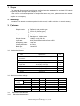
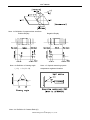
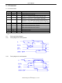
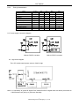
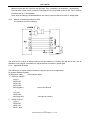
USER’S MANUAL FOR LCD MODULE EDM12864-116 Dalian Dongfu Color Display Co., Ltd. User’s Manual Contents 1. Scope --------------------------------------------------------------2 2. Warranty ----------------------------------------------------------2 3. Quality ----------------------------------------------------------2 4. Dimensional outline ------------------------------------------5 5. I/O terminals ----------------------------------------------------6 6. Quality level --------------------------------------------------11 7. Reliability -------------------------------------------------------14 8. Handling precaution ----------------------------------------14 9. Precaution for use ------------------------------------------15 10. Inclosure -----------------------------------------------------16 11. Part List -----------------------------------------------------------21 1 Dalian Dongfu Color Display Co., Ltd.. User’s Manual 1. Scope This manual defines general provisions as well as inspection standards for standard LCD module supplied by Dalian Dongfu Color Display Co.,LTD.. If the event of unforeseen problem or unspecified items may occur, please contact the nearest supplier or our company. 2. Warranty If module is not stored or used as specified in this manual, it will be void the 12- month warranty. 3. Features 3-1. Features Display mode : Reflective and positive type STN LCD (Yellow green) Display color: Display dot: Dark blue Background: Yellow green Display format: 128(w)×64 (h) full dots Input data: 8-bit parallel data interface from a MPU Multiplexing ratio: 1/64 Duty Viewing direction: 6 O’clock Back light:: None/LED Build-in DC/DC converter circuits 3-2.Mechanical features Item Specification Unit 93.0 (W)×70.0 (H) ×12.6 Max.(T) mm Number of dots 128 (W) ×64 (H) Dots — Viewing area 70.5 (W)×38.5 (H) mm Image area 66.52 (W)×33.24 (H) mm Dot pitch 0.52 (W)×0.52 (H) mm Dot size 0.48 (W)×0.48 (H) mm Weight Approx.100 g Outline dimensions 3-3. Absolute maximum ratings Item Supply Logic Voltage LCD drive Input Voltage Operating Temperature Storage Temperature Humidity 3-4. 3-4-1 Symbol Min. Max. Unit Vdd Vdd – Vee Vi Top Tstg — 0 0 0 -20 -25 — 6.0 16.0 Vdd 70 75 90 V V V ℃ ℃ %RH Electrical Characteristics Electrical Characteristics 2 Dalian Dongfu Color Display Co., Ltd.. Note User’s Manual Item Supply Symbol Logic Voltage Input Voltage Consumption Min. Typ. Max. 4.5 5.0 5.5 Vdd LCD drive Vdd–Vee “H” Level Vih “L” Level Logic 11.5 12.0 12.5 0.8Vdd — Vdd 0 — 0.2Vdd Fflm Vdd=5V 70 75 80 Idd Vdd=5V — — 2.8 — 0.15 0.2 — 12.6 13.0 11.5 12.0 12.5 11.0 11.4 — V Hz mA Vdd–Vee= 12.0V LCD drive Iee Fflm=75Hz Ta= 0℃ φ=0°,θ=0° LCD Driving Voltage Ta= 25℃ Vdd–Vee (Recommended Voltage) φ=0°,θ=0° Ta= 50℃ φ=0°,θ=0° Note: Unit Vdd=5V±5% Vil Frame Frequency Current Conditions <1> Duty =1/64 V <2> All dots on static state 3-4-2. Back light specifications for LED (The users can select the modules with or without backlight according to their own needs.) Item Unit Power supply V 2 Brightness Standard values Conditions Min. Typ. Max. — 4.2 — — cd/m (nit) — — — DC5.0 Vrms, Dark room Current mA — — 500 DC5.0 Vrms, Dark room Life time Hrs 10000 Note <1> Luminous color — Yellow green DC5.0 Vrms, Dark room Operating temperature ℃ -30 ~ 70 — Storage temperature ℃ -40 ~80 — Note<1>: Half value of initial brightness at 20℃ 60%RH 3-5. Electro-optical Characteristics Item Symbol LCD Driving Voltage VOP (Recommended voltage) (VDD-VO) Response Rise Time tr Time Decay Time Viewing angle Contrast Ratio Note: <1> Definition ofφandθ td Δφ K Temp. Conditions Min. — 12.6 13.0 φ=0°,θ=0° 11.5 12.0 12.5 0℃ 25℃ Typ. Max. 50℃ 11.0 11.4 — 0℃ — 1500 2000 — 150 200 — 3000 3500 — 200 250 Vertical -35 — 35 Horizontal -30 — 30 φ=0°,θ=0° 2.0 5.0 — 25℃ 0℃ φ=0°,θ=0° 25℃ 25℃ 25℃ <2> Contrast ratio higher than 2 (k≥2) voltage range. 3 Dalian Dongfu Color Display Co., Ltd.. Unit Note V 1,2,5 Ms 1,3,5 deg. 1,4,5 — 1,5,6 can be obtained in this User’s Manual Note: <3>Definition of response time waveform Positive Display Negative Display Note: <4>Definition of viewing angle (ΔΦ) ΔΦ=|Φ1-Φ2| Note: <5> Optical measuring system temperature-regulated chamber Note: <6> Definition of Contrast Ratio (K) 4 Dalian Dongfu Color Display Co., Ltd.. User’s Manual Positive Display Positive display Negative Display Brightness of non-selected dot (B2) Contrast (K)= Negative display Brightness of selected dot (B1) Brightness of non-selected dot (B1) Contrast (K)= Brightness of selected dot (B2) 4. Dimensional outline 93.0(PCB OUTLINE) 88.0 87.0(KJ) 70.5(V.A.) P0.52X127+0.48=66.52(I.A.) 12.6 MAX. 12.5 9.6 70.0(PCB OUTLINE) 65.0 50.0(KJ) 38.5(V.A.) P0.52X63+0.48=33.24(I.A.) 4- 3.0 8.0 PIN 1 2 3 4 5 6 7-14 15 16 17 18 19 20 20-φ1.0 20 0.52 0.48 1 P2.54X19=48.26 0.52 0.48 14.0 5 Dalian Dongfu Color Display Co., Ltd.. SYM. GND VDD VLCD RS RWL CE D0-D7 CS1 CS2 RST VADJ BL+ BL- User’s Manual 5. I/O terminal 5-1. I/O terminal table Pin No. 1 2 3 4 Pin name GND VDD VLCD D/I Level ---H/L 5 R/W H/L 6 E H.H→ L 7~14 15 DB0~DB7 CS1 H/L H/L 16 CS2 H/L 17 18 19 20 /RST VADJ BL+ BL- H/L ---- Functions Ground (0V) Power supply for logic circuit:+5V Operating voltage for LCD driving When D/I=“H”, it indicates that DB7~DB0 is display data; When D/I=“L”, it indicates that DB7~DB0 is instruction data. While R/W=“H” and E=“H” , data is read to DB7~DB0 While R/W=“L” and E=“H->L” , data is written to DB7~DB0 Enable signal. While R/W=“L”, data of DB7~DB0 is latched at falling edge of E While R/W=“H” and E=“H” , data of DD RAM appears at DB7~DB0 Data bus line. Chip selection. Selects the chip that controls the left half screen.( active at high level, CS1=1,CS2=0) Chip selection. Selects the chip that controls the right half screen.( active at high level, CS1=0,CS2=1) Controller reset at low level Negative voltage output Power Supply for LED Power Supply for LED ***Frame Ground must be soldering+ + 5-2. 5-2-1. Timing and timing diagram Timing diagram for write operation 5-2-2. Timing diagram for read operation 6 Dalian Dongfu Color Display Co., Ltd.. User’s Manual 5-2-3. Timing characteristics Name E cycle E High Level Width E Low Level Width E rise time E fall time Address setup time Address hold time Data set-up time Data delay time Write data hold time Read data hold time Symbol Min. 1000 450 450 140 10 200 10 20 Tcyc Pweh Pwel Tr Tf Tas Tah Tdsw Tddr Tdhw Tdhr Typ. - Max. 25 25 320 - Unit ns ns ns ns ns ns ns ns ns ns ns 5-3. Power supply connection diagram Without DC/DC converter Built-in DC/DC converter 5-4. Logic block diagram The LCD module needs power sources: Vdd for logic Note: It is necessary to guard all signals from external noise as signal lines are directly connected to C-MOS and are not pull-up or pull-down internally. 7 Dalian Dongfu Color Display Co., Ltd.. User’s Manual 5-5. Description for software and hardware 5-5-1. The internal structure of module From the above diagram, we may find that the module is mainly composed of LCD panel, controllers and segment drivers. The control circuit mainly consists of Instruction Register (IR), Data Register (DR), Busy Flag (BF), Display On/Off flip-flop (DFF) and XY Counter. ● Instruction Register (IR) IR stores instruction code. When D/I=0, the instruction is written into IR on the falling edge of E. ● Data Register (DR) DR stores data. When DR=1, graphic display data are written into DR or are read into DB7 to DB0 data buses under the action of E. The data transfer between DR and DDRAM are executed by internal operation automatically. ● Busy Flag (BF) Busy flag indicates that the module is operating or not operating. When BF=1, the module is in the internal operation and does not receive any external instruction and data. When BF=0, the module is in the ready status and can accept the data or instruction at any time. ● Display on/off flip-flop (DFF) The display on/off flip-flop makes on/off the liquid crystal display. When DFF=1, display on. The contents of DDRAM are on the screen. When DFF=0, display off. ● XY address counter XY address counter is a 9-bit counter. X address counter is higher 3 bits. Y address counter is lower 6 bits. In fact, XY address counter is used as the address pointer of DDRAM. X address counter is page address pointer of DDRAM. Y address counter is Y address pointer of DDRAM. ● Display Data RAM (DDRAM) DDRAM stores a display data for liquid crystal display. To express on state dot matrix of liquid crystal display, write data 1. The other way, off state writes 0. (See also DDRAM Address Table for the relation between the DDRAM address and the display position) ● Z Address Counter Z address counter is a 6-bit counter. It has cycle-count function, which is used to display with synchronous column scanning. When one column scanning is completed, the address counter is increased by 1 automatically and points to the next column scanning data. After reset, Z address counter is 0. Z address counter can be preset by DISPLAY START LINE instruction. Therefore, the display start line is controlled by this instruction. That is to say, where the DDRAM data start is the first line on the screen. There are 64 lines in DDRAM, which can be cycle-displayed on the screen. 5-5-2 Control instructions 1. Display ON/OFF R/W 0 2. D/I 0 DB7 0 DB6 0 DB5 1 DB4 1 DB3 1 DB2 1 DB1 1 DB0 D D=1 DISPLAY ON D=0 DISPLAY OFF. Internal status and display RAM data is not affected. When the value of D is changed from 0 into 1, the former display is on the screen. Display Start Line R/W 0 D/I 0 DB7 1 DB6 1 DB5 A5 DB4 A4 DB3 A3 DB2 A2 DB1 A1 8 Dalian Dongfu Color Display Co., Ltd.. DB0 A0 User’s Manual As explained above in Z address counter, the display start line is controlled by Z address counter. A5~A0 are automatically put into Z address counter. The address of start line can be any line of line 0 to line 63. For example: A5~A0 is selected 62, and the correspondence of the first line and DDRAM column is as follows: DD RAM Column: 62 63 0 1 2 3 ………… 60 61 Display column on the screen: 1 2 3 4 5 6 ………… 63 64 3. Set Page ( X ADDRESS ) DB7 DB6 DB5 DB4 DB3 DB2 DB1 DB0 R/W D/I 0 0 1 0 1 1 1 A2 A1 A0 Page address is line address of DDRAM. There are 8 lines in one page. There are 64 lines in DDRAM (8 pages). A2~A0 represent page 0 to page 7. Read/write data does not affect page address. Page address is changed by this instruction or RST signal. After reset, page address is 0. See also the address table for correspondence of page address and DDRAM. 4. Set Y Address R/W D/I DB7 DB6 DB5 DB4 DB3 DB2 DB1 DB0 0 0 0 1 A5 A4 A3 A2 A1 A0 The function of this instruction is to send A5~A0 to Y address counter. They are used as Y address pointer of DDRAM. Y address pointer is automatically incremented by 1 and points to the next unit of DDRAM after write/read is made to DDRAM. Table 4-4 DDRAM Address Table Y= 0 DB0 X=0 ↓ DB7 DB0 ↓ ↓ DB7 DB0 X=7 ↓ DB7 CS1=1, CS2=0 1 2 3 .. 062 63 DB0 ↓ DB7 DB0 ↓ DB7 DB0 ↓ DB7 0 DB0 ↓ DB7 DB0 ↓ DB7 DB0 ↓ DB7 1 CS1=0, CS2=1 2 3 .. 62 63 DB0 ↓ DB7 DB0 ↓ DB7 DB0 ↓ DB7 5. Line No. 0 ↓ 7 8 ↓ 55 56 ↓ 63 STATUS READ R/W D/I DB7 DB6 DB5 DB4 DB3 DB2 DB1 DB0 1 0 BF 0 ON/OFF RST 0 0 0 0 When R/W=1 and D/I=0, status read is output into the corresponding bits of data buses (DB7~DB0) (E in “H” level). BF: (See also BF part) ON/OFF: It means the status of Display On/Off flip-flop (See also Display On/Off flip-flop part) RST: When RST=1, it indicates that the system are in the initialization and any instruction and data except status read may not be accepted. 6. Write Display Data R/W D/I DB7 DB6 DB5 DB4 DB3 DB2 DB1 DB0 0 1 D7 D6 D5 D4 D3 D2 D1 D0 D7-D0 is display data. This instruction writes 8-bit data (D7-D0) into D7-D0 to the corresponding units of DDRAM. The Y address is incremented by 1 automatically. 7. Read Display Data R/W D/I DB7 DB6 DB5 DB4 DB3 DB2 DB1 DB0 1 1 D7 D6 D5 D4 D3 D2 D1 D0 9 Dalian Dongfu Color Display Co., Ltd.. User’s Manual Reads out 8-bit data (D7~D0) from the DD RAM. Then Y address is increased by 1 automatically. The instruction reads out the contents of DDRAM (D7-D0) to the data buses D7-D0. The Y address is incremented by 1 automatically Note: After the setting of DDRAM address, the dummy read is made at the time of reading data. 5-5-3 Method of interfacing module to MPU The interface circuit is as follows: The data bus P0 of 8031 is directly connected to the data bus of module. RD and WR of 8031 act as read/write control signal, interfaced to E signal terminal of module by NAND gate. 5-5-4. Application Example The following is to explain some instructions using the above circuit application. R0 (indirect address register) ID (instruction code) DATA (display data) 1. DISPLAY ON/OFF CLR P1 SETB RST SETB CS1 MOV A,#ID MOVX @R0,A ; the left 64 columns 2. ↓ CLR CS1 SETB CS2 MOVX @ R0,A READ STATUS CLR P1 SETB RST SETB CS1 SETB R/W ; the right 64 columns 10 Dalian Dongfu Color Display Co., Ltd.. User’s Manual 3. MOVX A,@R0 ;Status is read to A. WRITE DISPLAY DATA) Assuming that the addresses of X and Y has been set CLR P1 SETB RST SETB CS1 SETB D/I MOV A, # DATA MOVX @R0 , A ;Data is written into the corresponding units of DDRAM 6. Quality level 6-1 Inspection conditions 6-1-1The environmental conditions for inspection shall be as follows: Room temperature: 20±3℃ Humidity: 65±20% RH 6-1-2 The external visual inspection: The inspection shall be performed by using a 20W fluorescent lamp for illumination and the distance between LCD and the eyes of the inspector should be at least 30cm. 6-1-3 (1) Light method (2) Inspection distance and angle 6-2 Sampling procedures for each item’s acceptance level table Defect type Sampling procedure AQL MIL-STD-105D Inspection Level I Major defect Normal inspection Q/DF-01-98(II) Single sample inspection MIL-STD-105D Inspection Level I Minor defect Normal inspection Single sample inspection 6-3 Classification of defects 11 Dalian Dongfu Color Display Co., Ltd.. Q/DF-01-98(II) User’s Manual 6-3-1 Major defect A major defect refers to a defect that may substantially degrade usability for product applications. 6-3-2 Minor defect A minor defect refers to a defect that deviates from existing standards almost unrelated to the effective use of the product or its operation. 6-4 Inspection standards Item 1) Display on inspection Criterion for defects (1) Non display (2) Vertical line is deficient (3) Horizontal line is deficient (4) Cross line is deficient Size Φ(mm) Φ≤0.3 2) Black/White spot Defect type Major Acceptable number Ignore (note) 0.3<Φ≤0.45 3 0.45<Φ≤0.6 1 0.3<Φ 0 Minor (Note) Not allowed if four more spots crowd together Length (mm) Width (mm) L≤10 3) Black/White line Acceptable number W≤0.03 Ignore 5.0≤L≤10 0.03<W≤0.04 3 5.0≤L≤10 0.04<W≤0.05 2 1.0≤L≤10 0.05<W≤0.06 2 1.0≤L≤10 0.06<W≤0.08 L≤10 0.08<W Minor 1 follows 2) point defect Defects separate with each other at an interval of more than 20mm. 4) Display pattern Minor [Unit: mm] A+B≤0.45 0<C D+E≤0.35 F+G≤0.35 2 2 2 Note: 1) Up to 3 damages acceptable 2) Not allowed if there are two or more pinholes every threefourths inch. Item Criterion for defects Size Φ(mm) Φ≤0.7 5) Spot-like contrast irregularity Defect type Acceptable Number Ignore (note) 0.7<Φ≤1.0 3 1.0<Φ≤1.5 1 1.5<Φ 0 Note: 1) Conformed to limit samples. 2) Intervals of defects are more than 30mm. 12 Dalian Dongfu Color Display Co., Ltd.. Minor User’s Manual Size Φ(mm) Acceptable Number Φ≤0.4 0.4<Φ≤0.65 6) Bubbles in polarizer 0.65<Φ≤1.2 1.2<Φ 7) Scratches and dent on the polarizer 2 1 0 Scratches and dent on the polarizer shall be in the accordance with “2) Black/white spot”, and “3) Black/White line”. 8) Stains on the surface of LCD panel 9) Rainbow color 10) Viewing area encroachment 11) Bezel appearance 12) Defect of land surface contact Minor Ignore (note) Stains which cannot be removed even when wiped lightly with a soft cloth or similar cleaning. No rainbow color is allowed in the optimum contrast on state within the active area. Polarizer edge or line is visible in the opening viewing area due to polarizer shortness or sealing line. Minor Minor Minor Minor Rust and deep damages that are visible in the bezel are rejected. Minor Evident crevices that are visible are rejected. Minor (1) Failure to mount parts 13) Parts mounting (2) Parts not in the specifications are mounted Major (3) For example: Polarity is reversed, HSC or TCP falls off. 14) Part alignment (1) LSI, IC lead width is more than 50% beyond pad outline. (2) More than 50% of LSI, IC leads is off the pad outline. Major (1) 0.45<Φ, N≥1 15) Conductive foreign matter (solder ball, solder hips) (2) 0.3<Φ≤0.45, Minor N≥1 Minor Φ: Average diameter of solder ball (unit: mm) Minor (3) 0.5<L, N≥1 L: Average length of solder chip (unit: mm) (1) Deep damage is found on copper foil and the pattern is nearly 16) PCB pattern damage Major broken. (2) Damage on copper foil other than 1) above Minor (1) Due to PCB copper foil pattern burnout, the pattern is connected, using a jumper wire for repair;2 or more places are 17) Faulty PCB correction corrected per PCB. Minor (2) Short-circuited part is cut, and no resist coating has been performed. Item 18) Bezel flaw Criterion for defects Bezel claw missing or not bent Defect type Minor (1) Failure to stamp or label error, or not legible.(all acceptable if 19) Indication on name plate (sampling indication label) legible) (2) The separation is more than 1/3 for indication discoloration, in which the characters can be checked. 13 Dalian Dongfu Color Display Co., Ltd.. Minor User’s Manual 7. Reliability 7-1 Lifetime 50,000 hours (25℃ in the room without ray of sun) 7-2 Items of reliability Item Condition Criterion 1) High Temperature 50℃ No cosmetic failure is allowable. 96hrs Contrast ratio should be between initial Operating value ±10%. 2) Low -10℃ Temperature Total current consumption should be below 96hrs double of initial value. Operation 3) Humidity 4) 40℃, 90%RH, 96hrs High Temperature 5) Temperature shock 96hrs -20℃ 96hrs No cosmetic failure is allowable. Contrast ratio should be between initial Low 6) Thermal 60℃ value ±20%. 25℃→30℃→25℃→60℃ 5(min) 30(min) 5(min) 30(min) double of initial value. 5 cycle, 55~60%RH No defects in cosmetic and operational 10~55~10hz 7) Vibration Total current consumption should be below function are allowable. amplitude: 1.5mm 2hrs for each direction Total current consumption should be below double of initial value. (X,Y,Z) 8. Handling precautions 8-1 Mounting method A panel of LCD module made by Dalian Sanson Infortech Co., Ltd. consists of two thin glass plates with polarizers that easily get damaged. And since the module in so constructed as to be fixed by utilizing fitting holes in the printed circuit board (PCB), extreme care should be used when handling the LCD modules. 8-2 Cautions of LCD handling and cleaning When cleaning the display surface, use soft cloth with solvent (recommended below) and wipe lightly. Isopropyl alcohol Ethyl alcohol Trichlorotriflorothane Do not wipe the display surface with dry or hard materials that will damage the polarizer surface. Do not use the following solvent: Water Ketene Aromatics 8-3 Caution against static charge The LCD module use C-MOS LSI drivers. So we recommend you: Connect any unused input terminal to Vdd or Vss. Do not input any signals before power is turned on, and ground your body, work/assembly areas, assembly equipment to protect against static electricity. 14 Dalian Dongfu Color Display Co., Ltd.. User’s Manual 8-4 Packaging - Module employs LCD elements, and must be treated as such. Avoid intense shock and falls from a height. - To prevent modules from degradation, do not operate or store them exposed direct to sunshine or high temperature/humidity. 8-5 Caution for operation - It is an indispensable condition to drive LCD module within the limits of the specified voltage since the higher voltage over the limits may cause the shorter life of LCD module. An electrochemical reaction due to DC (direct current) causes LCD undesirable deterioration so that the uses of DC (direct current) drive should be avoided. - Response time will be extremely delayed at lower temperature than the operating temperature range and on the other hand at higher temperature LCD module may show dark color in them. However those phenomena do not mean malfunction or out of order of LCD module, which will come back in the specified operating temperature. 8-6 Storage In the case of storing for a long period of time, the following ways are recommended: - Storage in polyethylene bag with the opening sealed so as not to enter fresh air outside in it. And with not desiccant. - Placing in a dark place where neither exposure to direct sunlight nor light is. Keeping the storage temperature range. - Storing with no touch on polarizer surface by any thing else. 8-7 Safety - It is recommendable to crash damaged or unnecessary LCD into pieces and to wash off liquid crystal by either of solvents such as acetone and ethanol, which should be burned up later. - When any liquid leaked out of a damaged glass cell comes in contact with your hands, please wash it off well at once with soap and water. 9. Precaution for use 9-1 Both parties should provide a limit sample on an occasion when both parties agree its necessity. The judgement by a limit sample shall take effect after the limit sample has been established and confirmed by both parties 9-2 On the following occasions, the handling of problem should be decided through discussion and agreement between responsible of the both parties. - When a question is arisen in this manual. - When a new problem is arisen which is not specified in this manual. - Some problem is arisen due to the change of inspection and operating conditions in users. - When a new problem is arisen at the customer’s operating set for sample evaluation in the customer site. 15 Dalian Dongfu Color Display Co., Ltd..