1
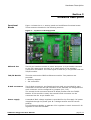
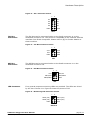
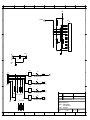
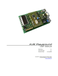
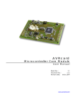
AVRcard’s Playground
Activity Board
User Manual
Board Rev.:
Document Rev.:
PRELIMINARY
Revision Date:
1.1
1.1a
13.11.2003
Copyright © 2003 by AVRcard.com
Product Overview
Contents
Product Overview
4
Key Features........................................................................ 4
Additional Resources ............................................................. 4
Getting started
5
Hardware Description
6
Functional Blocks.................................................................. 6
Header Connectors ............................................................... 7
Jumpers .............................................................................. 9
Circuit Diagrams
10
Bill of Materials................................................................... 11
Connectors Pinout Summary
12
References
15
Data Sheets ....................................................................... 15
Contact ............................................................................. 15
Figures
Figure 1 – Top View of the Playground .................................................. 6
Figure 2 - General Pinout of I/O Port Headers ........................................ 7
Figure 3 – A0-7 Connector Pinout......................................................... 8
Figure 4 – I2C Bus Connector Pinout..................................................... 8
Figure 5 – SPI Bus Connector Pinout..................................................... 8
Figure 6 – Monitoring LED Connector Pinout .......................................... 8
Figure 7 – Speaker Connector Schematic .............................................. 9
Figure 8 – Serial Port Configuration Jumpers ......................................... 9
Tables
Table 1 – List of Parts ....................................................................... 11
Table 2 – Port A Connector Pinout ...................................................... 12
Table 3 – Port B Connector Pinout ...................................................... 12
Table 4 – Port C Connector Pinout ...................................................... 12
Table 5 – Port D Connector Pinout ...................................................... 12
Table 6 – Port E Connector Pinout ...................................................... 13
Table 7 – Port F Connector Pinout ...................................................... 13
Table 8 – A0-7 Connector Pinout ........................................................ 13
Table 9 – I2C Connector Pinout.......................................................... 13
Table 10 – SPI Connector Pinout ........................................................ 14
Table 11 – Serial Port 2 Connector Pinout............................................ 14
AVRcard’s Playground User Manual
Rev. 1.1a, 13.11.2003
page 2/15
www.avrcard.com
Product Overview
Table 12 – LED Connector Pinout ....................................................... 14
Table 13 – SPKR Connector Pinout ..................................................... 14
AVRcard’s Playground User Manual
Rev. 1.1a, 13.11.2003
page 3/15
www.avrcard.com
Product Overview
Section 1
Product Overview
The AVRcard’s Playground has been designed as a base board for the AVRcard. It provides easy
connection options, and a number of additional features.
Key Features
Plug-in AVRcard with Atmega128 processor
Plug-in TCP/IP module
Plug-in 4x20 character LCD
Slot for MultiMedia Card
4 general purpose monitoring LEDs
Piezo speaker
Voltage regulator, allows for use of inexpensive power supply
Standard D-Sub connectors for both RS-232 interfaces
CPU ports routed to headers with STK500 compatible pinout
Separate connectors for I2C and SPI buses
Address bus demultiplexed
32Kbytes SRAM
Euro card size (100 x 160mm)
Additional
Resources
Product Information – All updated product information can be retrieved
at the Web Site, www.avrcard.com.
Application Support – Please check the Resources pages regularly at
www.avrcard.com for design notes and application hints. Further
support is available by email from [email protected].
Custom Designs – Custom population or customized versions of the
product are available. For inquiries please contact [email protected].
AVRcard’s Playground User Manual
Rev. 1.1a, 13.11.2003
page 4/15
www.avrcard.com
Getting started
Section 2
Getting started
Tbd.
AVRcard’s Playground User Manual
Rev. 1.1a, 13.11.2003
page 5/15
www.avrcard.com
Hardware Description
Section 3
Hardware Description
Functional
Blocks
Figure 1 shows the V1.1 activity board and its different functional areas.
These areas are detailed in the following sections.
Figure 1 – Top View of the Playground
AVRcard slot
Two 32-pin headers connect to power and ports. A 6-pin header connects
to the CPU reset signal, as there is no reset signal on the standard
connectors of AVRcard. The reset signal is used only in conjunction with the
TCP/IP module.
TCP/IP Module
This slot receives the IIM7010 Ethernet module. Two positions are
provided:
Memory mapped
I2C connection
D-Sub connectors
Two D-Sub connectors, one female and one male, are provided for easy
connection to the two RS-232 interfaces of the AVRcard. Pin assignment of
each connector can be configured by jumpers (J13, J15).
The second D-Sub connector shares its board position with the TCP/IP
Module. If this module is used, the second D-Sub connector can be
connected via the 10-pin header J18.
Power supply
A standard 7805 voltage regulator is provided for the 5V supply. DC power
is applied through the power jack J8. A bridge rectifier ensures correct
polarity.
For the Ethernet-Module, a separate 3.3V regulator is used. A second 3.3V
regulator is used for the MMC.
AVRcard’s Playground User Manual
Rev. 1.1a, 13.11.2003
page 6/15
www.avrcard.com
Hardware Description
External SRAM
The Playground contains a footprint for a 28-pin DIP socket (U3) where an
external SRAM device can be mounted. Make sure the SRAM device has the
same voltage range as the rest of the design.
Note: The SRAM is disabled by default. To enable SRAM support, put a
jumper on J14. The SRAM occupies the memory space from $1000-$7FFF.
LCD
A small alphanumeric LCD (4 lines, 20 characters) can be mounted across
the prototyping area (J25). The connector pinout is designed for the EA
DIP204-4 module from Electronic Assembly. It is connected to the SPI bus.
Please refer to [5] for further details on this display.
Display contrast is adjusted by R5. R4 sets the background LED current.
MMC Connector
An adapter for MultiMediaCards (MMC) can be mounted on position J17.
The MMC is connected to the SPI bus via level converters 74VHC08 (U6).
Bit5 of PortB is used as SS signal in order not to interfer with the standard
SPI Bus Connection.
Header
Connectors
All CPU ports and some additional signals can be connected by standard
0.1” headers. Pin 1 has a square pad.
Port Connectors
The pinout for the I/O port headers is explained in Figure 2. The square
marking indicates pin 1.
Figure 2 - General Pinout of I/O Port Headers
1
2
Px0
Px1
Px2
Px3
Px4
Px5
Px6
Px7
GND
VCC
PORTx
A0-7 Connector
The connector J20, marked A0-7 contains the 8 least-significant bits of the
external address bus. The purpose of the connector is to provide easy
access to the address bus. The 8 most significant bits can be found on the
Port C connector J4.
This connector is handy when interfacing external devices.
AVRcard’s Playground User Manual
Rev. 1.1a, 13.11.2003
page 7/15
www.avrcard.com
Hardware Description
Figure 3 – A0-7 Connector Pinout
1
2
A0
A1
A2
A3
A4
A5
A6
A7
GND
VCC
A0-7
I2C Bus
Connection
The I2C bus can be connected either to the PortD connector or to the
dedicated connector J12. This pinout is compatible to the modules with I2C
interface from E-Lab Computers. Please refer to [6] for further details on
these modules.
Figure 4 – I2C Bus Connector Pinout
1
2
VCC
VCC
SCL
SDA
GND
GND
I2C
SPI Bus
Connection
The SPI bus can be connected either to the PortB connector or to the
dedicated connector J16.
Figure 5 – SPI Bus Connector Pinout
1
2
VCC
PB0/SS
PB1/SCK
PB2/MOSI
PB3/MISO
GND
SPI
LED Connector
Four general purpose monitoring LEDs are provided. The LEDs are drived
by the hex inverter U11. Figure 6 shows the pinout of J23.
Figure 6 – Monitoring LED Connector Pinout
1
2
LED0 (D3)
LED1 (D4)
LED2 (D5)
LED3 (D6)
GND
VCC
LED 0-3
AVRcard’s Playground User Manual
Rev. 1.1a, 13.11.2003
page 8/15
www.avrcard.com
Hardware Description
Piezo Speaker
Connector
A piezo speaker can be connected to any port to deliver audible signals.
The figure below shows the pinout of the speaker connector J5
Figure 7 – Speaker Connector Schematic
C9
10uF
PIEZO
U10
+
HDR_2
1
2
2
1
J5
GND
Jumpers
Jumpers are standard (0.1").
Pinout Selection
for D-Sub
The RXD and TXD signals can be interchanged on each of the D-Sub
connectors. Figure 8 applies to J13 and J15.
Figure 8 – Serial Port Configuration Jumpers
1 2
To pin 3 of D-Sub
TXD
RXD
To pin 2 of D-Sub
PORTx
External Power
Enable
If the AVRcard is powered from a battery hrough the DC-DC converter, the
jumper J9 must be left open.
Mode Selection for
Ethernet-Module
When the Ethnernet module is used in memory-mapped mode, closing of
jumper J19 selects the non clocked mode. Please refer to [4] for further
details.
AVRcard’s Playground User Manual
Rev. 1.1a, 13.11.2003
page 9/15
www.avrcard.com
Circuit Diagrams
Section 4
Circuit Diagrams
The diagrams on the following pages are also availabe in a separate
document.
AVRcard’s Playground User Manual
Rev. 1.1a, 13.11.2003
page 10/15
www.avrcard.com
7
6
PORTBUS
RD
VCC
U3
A0
A1
A2
A3
A4
A5
A6
A7
10
9
8
7
6
5
4
3
25
24
21
23
2
26
1
PA0
11
PA1
12
PA2
13
PA3
15
PA4
16
PA5
17
PA6
18
PA7
19
B
1
11
ALE
PA0
GND
3
PA1
4
PA2
7
PA3
PA4
8
PA5
14
PA6
17
PA7
18
13
52256
A0
CS
A1
WR
A2
RD
A3
A4
A5
A6
A7
A8
A9
A10
A11
A12
A13
A14
7
1
AVRCARD CONNECTORS
D
PE0
PE1
PE2
PE3
PE4
PE5
PE6
PE7
PB0
PB1
PB2
PB3
PB4
PB5
PB6
PB7
PD0
PD1
PD2
PD3
PD4
PD5
PD6
PD7
20
27
22
J14
1
2
HDR_2
SET JUMPER TO SET RAM ADDR
TO $1000-$7FFF
D0
D1
D2
D3
D4
RXD1
RXD2
TXD1
TXD2
D5
D6
33
34
35
36
37
38
39
40
41
42
43
44
45
46
47
48
49
50
51
52
53
54
55
56
57
58
59
60
61
62
63
64
PE0/RXD
PE1/TXD
PE2/AC+
PE3/ACPE4/INT4
PE5/INT5
PE6/INT6
PE7/INT7
PB0/SS
PB1/SCK
PB2/MOSI
PB3/MISO
PB4/OC0
PB5/OC1A
PB6/OC1B
PB7/OC2
PD0/INT0
PD1/INT1
PD2/INT2
PD3/INT3
PD4/IC1
PD5/
PD6/T1
PD7/T2
VCC
VCC
GND
GND
RX1
RX2
TX1
TX2
PC0
PC1
PC2
PC3
PC4
PC5
PC6
PC7
PA7
PA6
PA5
PA4
PA3
PA2
PA1
PA0
ALE
RD
WR
1
PC0/A8
2
PC1/A9
3
PC2/A10
4
PC3/A11
5
PC4/A12
6
PC5/A13
7
PC6/A14
8
PC7/A15
9
PA7/AD7
10
PA6/AD6
11
PA5/AD5
12
PA4/AD4
13
PA3/AD3
14
PA2/AD2
15
PA1/AD1
16
PA0/AD0
17
ALE
18
RD
19
WR
20
SQW
21
VCC
22
VCC
23
GND
24
GND
25
PF7/ADC7
26
PF6/ADC6
27
PF5/ADC5
28
PF4/ADC4
29
PF3/ADC3
30
PF2/ADC2
31
PF1/ADC1
32
PF0/ADC0
C
PF7
PF6
PF5
PF4
PF3
PF2
PF1
PF0
D7
EN
C1
RS-232
Ü
1D
1Q
2D
2Q
3D
3Q
4D
4Q
5D
5Q
6D
6Q
7D
7Q
8D
AVRCARD_1
GND
U2
8Q
2
A0
5
A1
6
A2
9
A3
12
A4
15
A5
16
A6
19
A7
74AHC373
8
2
PC7
VCC
PC0
PC1
PC2
PC3
PC4
PC5
PC6
A
3
R1
ADRBUS
C
4
10k
D
WR
5
VCC
8
6
5
4
U4
REV: 1.1
DATE:
28.10.2003
ENG: HK
REV: 1.0
DATE:
9.7.2003
ENG: HK
PROJECT:
AVRCARD'S PLAYGROUND
COMPANY:
ADDRESS:
CITY
COUNTRY:
AVRCARD.COM
STEINACKERWEG 14
CH-3075 RUEFENACHT
SWITZERLAND
INITIAL
3
B
GND
9.7.2003
A
PAGE:
2
1
OF:
6
1
8
7
6
5
4
3
2
1
PORTBUS
D
D
VCC
1
2
3
4
5
6
7
8
9
10
HDR_10
GND
PE0
PE1
PE2
PE3
PE4
PE5
PE6
PE7
HDR_10
J7
PD0
PD1
PD2
PD3
PD4
PD5
PD6
PD7
PF0
PF1
PF2
PF3
PF4
PF5
PF6
PF7
1
2
3
4
5
6
7
8
9
10
HDR_10
GND
J12
1
2
3
4
5
6
SCL
SDA
PD0
PD1
HDR_6
VCC
1
2
3
4
5
6
7
8
9
10
C
J16
1
2
3
4
5
6
SS
SCK
MOSI
MISO
PB0
PB1
PB2
PB3
HDR_6
GND
VCC
J22
VCC
HDR_10
VCC
HDR_10
PB0
PB1
PB2
PB3
PB4
PB5
PB6
PB7
1
2
3
4
5
6
7
8
9
10
J3
J6
PC0
PC1
PC2
PC3
PC4
PC5
PC6
PC7
VCC
HDR_10
1
2
3
4
5
6
7
8
9
10
J4
VCC
C
PA0
PA1
PA2
PA3
PA4
PA5
PA6
PA7
1
2
3
4
5
6
7
8
9
10
J1
GND
B
B
ADDRBUS
A0
A1
A2
A3
A4
A5
A6
A7
1
2
3
4
5
6
7
8
9
10
VCC
J20
HDR_10
A
GND
REV: 1.1
DATE:
28.10.2003
ENG: HK
REV: 1.0
DATE:
9.7.2003
ENG: HK
PROJECT:
AVRCARD'S PLAYGROUND
COMPANY:
ADDRESS:
CITY
COUNTRY:
AVRCARD.COM
STEINACKERWEG 14
CH-3075 RUEFENACHT
SWITZERLAND
INITIAL
8
7
6
5
4
3
9.7.2003
A
PAGE:
2
2
OF:
6
1
1
4
1
PWR JACK
3 BRIDGE
+
C1
GND
VOUT
GND
3
C2
LM341T
1
J9
2
D
VCC
C5
C6
.1uF
.1uF
R2
47uF
.1uF
GND
ZSR330C U8
GND
D1
GND
U5
VIN
3
2
1
G1
4
HDR_2
2
1
3
5
2
J8
D
6
330E
7
Power LED
8
C4
GND
IN
GND
VDD
OUT
C3
GND
.1uF
C
GND
.1uF
GND
C
GND
GND
ZSR330C
C8
J21
1
2
GND
IN
U7
VDD2
OUT
C7
GND
.1uF
.1uF
HDR_2
GND
GND
GND
B
B
A
REV: 1.1
DATE:
28.10.2003
ENG: HK
REV: 1.0
DATE:
4.7.2003
ENG: HK
PROJECT:
AVRCARD'S PLAYGROUND
COMPANY:
ADDRESS:
CITY
COUNTRY:
AVRCARD.COM
STEINACKERWEG 14
CH-3075 RUEFENACHT
SWITZERLAND
INITIAL
8
7
6
5
4
3
9.7.2003
A
PAGE:
2
3
OF:
6
1
8
7
6
5
4
3
2
1
PORTBUS
RS-232
D
D
J13
74VHC08
3
VDD
CS
SI
J17
C
SCK
SO
B
Y
A
&
U6.A
74VHC08
1
2
3
4
5
6
7
6
B
Y
A
&
U6.B
PB5
8
B
Y
A
&
U6.C
GND
J15
J10
1
PB2
4
J11
J18
10
9
J2
PB3
HDR_2
1
2
3
4
5
6
7
8
9
C
DELTA_9HM
DELTA_9HF
PB1
TXD2
RXD2
HDR_4
1
2
3
4
5
6
7
8
9
5
1
2
3
4
TXD1
RXD1
HDR_4
2
74VHC08
HDR_7
1
2
3
4
1
2
GND
1
2
3
4
5
6
7
8
9
10
HDR_10
B
A
B
Y
74VHC08
11
D2
1k
VDD
13
U6.D
&
R3
12
LED SELECT
A
REV: 1.1
DATE:
28.10.2003
ENG: HK
REV: 1.0
DATE:
4.7.2003
ENG: HK
PROJECT:
AVRCARD'S PLAYGROUND
COMPANY:
ADDRESS:
CITY
COUNTRY:
AVRCARD.COM
STEINACKERWEG 14
CH-3075 RUEFENACHT
SWITZERLAND
INITIAL
8
7
6
5
B
GND
4
3
9.7.2003
A
PAGE:
2
4
OF:
6
1
8
7
6
5
4
3
2
1
PORTBUS
D
ADRBUS
J19
C
VDD2
SELECT
NON-CLOCKED
MODE
1
2
1
52
25
26
27
HDR_2
PA0
PA1
PA2
PA3
PA4
PA5
PA6
PA7
44
43
46
45
48
47
50
49
34
36
38
39
40
53
54
B
28
VDD
VDD
MODE0
MODE1
MODE2
EXT CLK
23
22
21
20
19
18
17
16
15
14
11
12
9
10
7
A0
A1
A2
A3
A4
A5
A6
A7
A8
A9
A10
A11
A12
A13
A14
L_COL
L_100ACT
L_10ACT
L_DUPX
L_LINK
SCL
SDA
2
3
4
5
6
30
ÎNT
WR
RD
CS
RESET
RESET
D0
D1
D2
D3
D4
D5
D6
D7
I2C MODE
SLAVE ADDR: $7F
VDD2
MEMORY MODE
MEM ADDR: $8000-$FFFF
PE5
WR
RD
PC0
PC1
PC2
PC3
PC4
PC5
PC6
1
52
25
26
27
A0
A1
A2
A3
A4
A5
A6
A7
44
43
46
45
48
47
50
49
34
36
38
39
40
PD0
PD1
53
54
IIM7010A
28
U11.E
1
U1
PC7
11
A
Y
VDD
VDD
MODE0
MODE1
MODE2
ÎNT
WR
RD
CS
RESET
RESET
D0
D1
D2
D3
D4
D5
D6
D7
A0
A1
A2
A3
A4
A5
A6
A7
A8
A9
A10
A11
A12
A13
A14
L_COL
L_100ACT
L_10ACT
L_DUPX
L_LINK
SCL
SDA
EXT CLK
2
3
4
5
6
30
C
23
22
21
20
19
18
17
16
15
14
11
12
9
10
7
GND
VDD2
D
B
IIM7010A_1
U9
10
74HC04
J24
A
1
2
3
4
5
6
13
U11.F
1
A
Y
12
74HC04
HDR_6
REV: 1.1
DATE:
28.10.2003
ENG: HK
REV: 1.0
DATE:
4.7.2003
ENG: HK
PROJECT:
AVRCARD'S PLAYGROUND
COMPANY:
ADDRESS:
CITY
COUNTRY:
AVRCARD.COM
STEINACKERWEG 14
CH-3075 RUEFENACHT
SWITZERLAND
INITIAL
8
7
6
5
4
3
9.7.2003
A
PAGE:
2
5
OF:
6
1
8
7
6
5
4
3
2
1
VCC
R7
PORTBUS
LCD
27k
D
PB4
PB2
PB1
PB3
R4
22E
R5
10k
C
1
2
3
4
5
6
7
8
9
10
11
12
13
14
15
16
17
18
D
J25
GND
VCC
V0
RS
R/W
E
D4
D5
D6
D7
RES
LED-A
LED_C
C
GND
A
Y
8
74HC04
5
HDR_6
U11.C
1
A
Y
LED 3MM VER. GREEN
6
74HC04
3
R8.A
R8.B
R8.C R8.D
1
A
VCC
R6.FR6.GR6.H
GND
U11.B
1
A
Y
74HC04
U11.A
1
A
Y
74HC04
D3
D4
LED 3MM VER. GREEN
4
D5
LED 3MM VER. GREEN
2
B
VCC
9
R6.A
1
2
3
4
5
6
U11.D
1
R6.B
J23
J5
R6.C
B
2
1
GND
D6
LED 3MM VER. GREEN
R6.D
PIEZO
U10
C9
10uF
-
1
2
+
HDR_14
HDR_2
REV: 1.1
DATE:
28.10.2003
ENG: HK
REV: 1.0
DATE:
4.7.2003
ENG: HK
PROJECT:
AVRCARD'S PLAYGROUND
COMPANY:
ADDRESS:
CITY
COUNTRY:
AVRCARD.COM
STEINACKERWEG 14
CH-3075 RUEFENACHT
SWITZERLAND
INITIAL
8
R6.E
7
6
5
4
3
9.7.2003
A
PAGE:
2
6
OF:
6
1
Circuit Diagrams
Table 1 – List of Parts
Bill of Materials
Qty
Description
Value
Case
RefDefs
1
SRAM
52256
DIP28
U3
1
Demultiplexer
74AHC373
DIP20
U2
1
Hex Inverter
74HC04
DIP14
U11
1
Level converter
74VHC08
DIP14
U6
1
AVRCARD V1.1
-
1
BRIDGE
1
DELTA_9HF
DELTA_9HF
J10
1
DELTA_9HM
DELTA_9HM
J11
1
ELCO
10uF
ELKO5R2_5
C9
1
ELCO
47uF
ELKO5R2_5
C1
1
Header
HDR 1x2
1
MMC_SLOT
HDR_7
1
Ethernet Module
IIM7010A
1
LED
LED red
LED green
U4
BR-DL
G1
J2
MMC_SLOT
J17
U1 or U9
3mm vert.
D1
1
LED
1
PIEZO
3mm vert.
D2
BUZZER12R10
U10
1
POT.METER_2
10k
1
PWR JACK
HDR_2
1
Resistor Array 8
10k
HEADER1X9
1
Resistor Array 4
1k
HEADER1X5
1
Resistor
10k
R1
1
Resistor
1k
R3
1
Resistor
22E
R4
1
Resistor
27k
R7
R5
J8
R8
R6
1
Resistor
330E
2
Voltage Regulator
ZSR330C
78LXX
U7, U8
R2
2
Header
HDR_4
HDR2X2
J13, J15
4
Header
HDR_6
HDR2X3
J12, J16, J23,
J24
4
LED
LED yellow
3mm vert.
D3, D4, D5, D6
5
Header
HDR_2
HDR1X2
J9, J5, J14, J19,
J21
7
CAPACITOR
0.1uF
8
Header
HDR_10
C2, C3, C4, C5,
C6, C7, C8
HDR2X5
J1, J3, J4,J6, J7,
J18, J20, J22
1
LCD
EA DIP204-4
EA_DIP_LCD
J25
1
Voltage Regulator
LM341T
TO220H
U5
AVRcard’s Playground User Manual
Rev. 1.1a, 13.11.2003
page 11/15
www.avrcard.com
Connectors Pinout Summary
Section 5
Connectors Pinout Summary
J1
Table 2 – Port A Connector Pinout
Pin
Function
Alt. Function
I/O
Internal Connections
1
2
3
4
5
6
7
8
9
10
PA0
PA1
PA2
PA3
PA4
PA5
PA6
PA7
GND
VCC
AD0
AD1
AD2
AD3
AD4
AD5
AD6
AD7
I/O
I/O
I/O
I/O
I/O
I/O
I/O
I/O
PWR
PWR
U3/D0,
U3/D1,
U3/D2,
U3/D3,
U3/D4,
U3/D5,
U3/D6,
U3/D7,
U1/D0,
U1/D1,
U1/D2,
U1/D3,
U1/D4,
U1/D5,
U1/D6,
U1/D7,
U2/0D
U2/1D
U2/2D
U2/3D
U2/4D
U2/5D
U2/6D
U2/7D
J3
Table 3 – Port B Connector Pinout
J4
J22
Pin
Function
Alt. Function
I/O
Internal Connections
1
2
3
4
5
6
7
8
9
10
PB0
PB1
PB2
PB3
PB4
PB5
PB6
PB7
GND
VCC
SS
SCK
MOSI
MISO
OC0
OC1A
OC1B
OC2
I/O
I/O
I/O
I/O
I/O
I/O
I/O
I/O
PWR
PWR
J16/2
J16/3, MMC/5 (via U6), LCD/6
J16/4, MMC/2 (via U6), LCD/5
J16/5, MMC/7, LCD/7
LCD/4
MMC/1 (via U6)
Table 4 – Port C Connector Pinout
Pin
Function
Alt. Function
I/O
Internal Connections
1
2
3
4
5
6
7
8
9
10
PC0
PC1
PC2
PC3
PC4
PC5
PC6
PC7
GND
VCC
A8
A9
A10
A11
A12
A13
A14
A15
I/O
I/O
I/O
I/O
I/O
I/O
I/O
I/O
PWR
PWR
U3/A8, U1/A8
U3/A9, U1/A9
U3/A10, U1/A10
U3/A11, U1/A11
U3/A12, U1/A12
U3/A13, U1/A13
U3/A14, U1/A14
U3/CS (via J14), U1/CS (inverted)
Table 5 – Port D Connector Pinout
Pin
1
2
3
4
5
Function
Alt. Function
I/O
Internal Connections
PD0
PD1
PD2
PD3
PD4
INT0/SCL
INT1/SDA
INT2
INT3
I/O
I/O
I/O
I/O
I/O
J12/3
J12/4
AVRcard’s Playground User Manual
Rev. 1.1a, 13.11.2003
page 12/15
www.avrcard.com
Connectors Pinout Summary
J6
J7
Pin
Function
Alt. Function
I/O
6
7
8
9
10
PD5
PD6
PD7
GND
VCC
IC1
T1
T2
I/O
I/O
I/O
PWR
PWR
Internal Connections
Table 6 – Port E Connector Pinout
Pin
Function
Alt. Function
I/O
1
2
3
4
5
6
7
8
9
10
PE0
PE1
PE2
PE3
PE4
PE5
PE6
PE7
GND
VCC
RXD
TXD
AC+
ACINT4
INT5
INT6
INT7
I/O
I/O
I/O
I/O
I/O
I/O
I/O
I/O
PWR
PWR
Internal Connections
Table 7 – Port F Connector Pinout
Pin
Function
Alt. Function
I/O
1
2
3
4
5
6
7
8
9
10
PF0
PF1
PF2
PF3
PF4
PF5
PF6
PF7
GND
VCC
ADC0
ADC1
ADC2
ADC3
ADC4
ADC5
ADC6
ADC7
I/O
I/O
I/O
I/O
I/O
I/O
I/O
I/O
PWR
PWR
Internal Connections
J20
Table 8 – A0-7 Connector Pinout
Pin
Function
1
2
3
4
5
6
7
8
9
10
A0
A1
A2
A3
A4
A5
A6
A7
GND
VCC
Alt. Function
I/O
Internal Connections
I/O
I/O
I/O
I/O
I/O
I/O
I/O
I/O
PWR
PWR
U3/A0,
U3/A1,
U3/A2,
U3/A3,
U3/A4,
U3/A5,
U3/A6,
U3/A7,
I/O
Internal Connections
PWR
PWR
I/O
I/O
PWR
PWR
J22/1
J22/2
U2/1Q,
U2/2Q,
U2/3Q,
U2/4Q,
U2/5Q,
U2/6Q,
U2/7Q,
U2/8Q,
U1/A0
U1/A1
U1/A2
U1/A3
U1/A4
U1/A5
U1/A6
U1/A7
J12
Table 9 – I2C Connector Pinout
Pin
1
2
3
4
5
6
Function
VCC
VCC
SCL
SDA
GND
GND
AVRcard’s Playground User Manual
Rev. 1.1a, 13.11.2003
Alt. Function
page 13/15
www.avrcard.com
Connectors Pinout Summary
J16
Table 10 – SPI Connector Pinout
Pin
1
2
3
4
5
6
Function
Alt. Function
VCC
SS
SCK
MOSI
MISO
GND
I/O
Internal Connections
PWR
I/O
I/O
I/O
I/O
PWR
J3/0
J3/1
J3/2
J3/3
J18
Table 11 – Serial Port 2 Connector Pinout
Pin
1
2
3
4
5
6
7
8
9
10
Function
Alt. Function
I/O
Internal Connections
RXD
TXD
I/O
I/O
J15/4
J15/1
GND
PWR
J23
Table 12 – LED Connector Pinout
Pin
1
2
3
4
5
6
Function
Alt. Function
D3
D4
D5
D6
GND
VCC
I/O
Internal Connections
I
I
I
I
PWR
PWR
U11/9
U11/5
U11/3
U1/1
I/O
Internal Connections
Table 13 – SPKR Connector Pinout
Pin
1
2
Function
GND
SPKR
AVRcard’s Playground User Manual
Rev. 1.1a, 13.11.2003
Alt. Function
PWR
I
page 14/15
www.avrcard.com
References
Section 6
References
Data Sheets
Contact
[1]
ATmega128:
www.atmel.com
[2]
FM24C256-SE:
www.ramtron.com
[3]
DS1307, MAX202, MAX485, MAX1674: www.maxim-ic.com
[4]
Ethernet-Module IIM7010A
www.i2chip.com
[5]
EA DIP204-4 LCD
www.lcd-module.de
[6]
E-Lab Computers
www.e-lab.de
Elektronik-Atelier
Hans Kallen
Steinackerweg 14
CH-3075 Rüfenacht
Switzerland
www.avrcard.com
[email protected]
Phone: +41 31 832 1441
Fax:
+41 31 832 1442
AVRcard’s Playground User Manual
Rev. 1.1a, 13.11.2003
page 15/15
www.avrcard.com