1
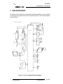
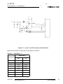
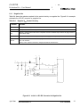
CL-PS7111 Application Note — AN-PS1 CL-PS7111 Evaluation Kit User Manual Portable Systems Cirrus Logic Inc. Scope and Applicability The CL-PS7111 evaluation kit (Order no. CL-PSK7111DM01) is offered by Cirrus Logic to assist system designers in building CL-PS7111–based systems and developing and debugging drivers and application programs for this highly integrated microcontroller. The evaluation kit provides software and hardware support to evaluate performance and measure power consumption under various conditions. This kit contains a reference board to be used as the starting point for new designs. A system designer can elect to use the board as the ‘motherboard’ and simply add application-specific I/O modules to the board. For example, the designer of a two-way pager can incorporate the pager functionality as an I/O module attached to the basic board. All engineering design collateral is provided in this kit. System Requirements The preloaded debug monitor requires a PC running the symbolic debug monitor PC (DOS or Windows 95). Contact ARM at www.arm.com or Cirrus Logic to order the ARM toolkit containing a C-compiler, linker, and assembler. Familiarity with the ARM tools, such as ARMSD and/or Tool 200, is required to use the evaluation board. Copyright 1997 — Cirrus Logic Inc. All rights reserved. This document describes a potential application of Cirrus Logic Inc. integrated circuits. No warranty is given for the suitability of the circuitry or program code described herein for any purpose other than demonstrating functional operation. The information contained in this document is subject to change without notice. Version 1.0 AN146REV1 APR '97 CL-PS7111 Evaluation Kit — User Manual Table of Contents List of Figures .......................................................................................... 3 List of Tables ............................................................................................. 3 1. INTRODUCTION ........................................................................................ 4 1.1 Ordering Information ................................................................................................ 4 2. EVALUATION KIT CONTENTS ................................................................. 5 2.1 Options ..................................................................................................................... 5 3. EVALUATION BOARD ............................................................................... 6 3.1 3.2 3.2.1 3.2.2 3.2.3 3.3 3.3.1 3.3.2 3.4 3.4.1 3.4.2 3.4.3 3.4.4 3.4.5 3.5 3.6 3.6.1 3.6.2 3.7 3.8 3.9 3.10 3.11 3.12 Main Feature Set ...................................................................................................... 7 Board Revisions ....................................................................................................... 8 Software Revision .............................................................................................. 8 Endian Operation ............................................................................................... 8 Stuffing Options ................................................................................................. 8 Board Setup ............................................................................................................. 9 Power ................................................................................................................. 9 LCD ................................................................................................................... 9 Boot Sequence ........................................................................................................ 9 Boot Program Resize to 2 Kbytes .................................................................... 10 Boot Program File Format ............................................................................... 11 Booting with Start Up Sequence from the Serial Port ..................................... 11 Start Up Sequence Using Preinstalled Debug Monitor (DEMON) ................... 12 Configure the ARM Debugger for Windows (Tool v2.1) ................................. 13 Board Layout .......................................................................................................... 14 Memory Architecture .............................................................................................. 18 Memory Map in Operating Mode ..................................................................... 19 Memory Map in Boot Mode ............................................................................. 19 I/O Port Allocation .................................................................................................. 20 Analog-to-Digital Converter .................................................................................... 21 LCD Interface ......................................................................................................... 21 J1 Connector Pinout .............................................................................................. 22 J24 Connector Pinout ............................................................................................ 23 Codec ..................................................................................................................... 23 4. DESIGN FILES ........................................................................................ 24 4.1 4.2 System Board ........................................................................................................ 24 Key Board............................................................................................................... 24 5. BOOT CODE AND DEMON FILES ......................................................... 24 6. POWER SUPPLY DESIGN ...................................................................... 25 6.1 6.2 Step-up Converter .................................................................................................. 25 Step-Down Converter ............................................................................................. 26 7. MEASURING CL-PS7111 POWER CONSUMPTION ............................. 27 2 Table of Contents APPLICATION NOTE v1.0 April 1997 CL-PS7111 Evaluation Kit — User Manual 8. DC-DC CONVERTER .............................................................................. 28 8.1 Setup Procedure .................................................................................................... 28 8.1.1 Negative VEE .............................................................................................................................. 31 8.1.2 VPP Control ...................................................................................................... 32 9. PC Card (PCMCIA) Interface .................................................................. 33 9.1 9.1.1 9.2 9.3 9.4 9.5 9.6 PC Card Power Switches at Multiple Points ........................................................... 33 PC Card Power ................................................................................................ 33 CL-PS7111-to-CL-PS6700 Interconnect Diagram ................................................. 34 Interrupts ................................................................................................................ 34 DMA Support ......................................................................................................... 34 Power Down ........................................................................................................... 34 Clocks .................................................................................................................... 35 A. Source Address Locator ........................................................................ 36 B. Bill of Materials ....................................................................................... 37 C. Schematics ............................................................................................. 46 List of Figures Figure 3-1 3-2 8-1 8-2 9-1 Page CL-PS7111 Evaluation Board Block Diagram ............................................. 6 Null-Modem Cable ...................................................................................... 9 CL-PS7111 DC-DC Converter for Positive VEE .................................................... 29 CL-PS7111 DC-DC Converter for Negative VEE .................................................. 31 CL-PS7111-to-CL-PS6700 Interconnect Diagram .................................... 34 List of Tables Table April 1997 Page 3-1 Assembly Instruction ................................................................................... 8 3-2 3-3 3-4 3-5 3-6 3-7 7-1 8-1 8-2 8-3 8-4 Boot Software Programs ........................................................................... 10 Port Allocation Pin Configuration .............................................................. 20 J2 Connector Pins ..................................................................................... 21 Compatible Panels .................................................................................... 22 J1 Connector Pins ..................................................................................... 22 J24 Pin Connections ................................................................................. 23 Typical Current Values at Various Conditiona ............................................ 27 VEE Control Circuitry ................................................................................. 28 Duty Ratio = 5 ........................................................................................... 29 Duty Ratio = 2 ........................................................................................... 30 Negative VEE Control Circuitry .................................................................. 31 8-5 9-1 DC-DC Pump Ratio = 5 ............................................................................. 32 Switch Settings .......................................................................................... 33 APPLICATION NOTE v1.0 List of Figures 3 CL-PS7111 Evaluation Kit — User Manual 1. INTRODUCTION The CL-PS7111 evaluation kit is targeted for system designers who are developing CL-PS7111–based platforms. This kit is also for software developers who plan to port operating systems and applications to the CL-PS7111. To use the CL-PS7111 evaluation kit, the ARM toolkit containing the C-compiler, linker and assembler, debugger, and ARM instruction set emulators is required. The CL-PS7111 evaluation kit is intended to be used with the ARM toolkit running on a PC with DOS, Windows 3.1 or Windows 95 installed. 1.1 Ordering Information The following presents part numbering ordering information: 4 ● CL-PS7111 Evaluation Kit: CL-PS7111-DMBD01 ● ARM toolkit: PSKARMTOOL-01 INTRODUCTION APPLICATION NOTE v1.0 April 1997 CL-PS7111 Evaluation Kit — User Manual 2. EVALUATION KIT CONTENTS The evaluation kit contains: ● CL-PS7111 evaluation board ● Keyboard — X/Y key matrices ● LCD Panel — 240 × 100 pixels, 3.3-V Cirrus Logic, or — 320 × 240 pixels, 3.3-V Alps ● Maxim data sheets — Step-up/down converter — A/D converter ● Oki America, Inc. data sheets — Telephone codec, MSM7702 — Speaker amplifier, MSC1192 ● ARM710 core data book ● 9-V AC/DC adapter ● CL-PS7111 demonstration program disk ● Schematic layout disk ● CL-PS7111 data book ● 2 null-modem cables ● ARM debug monitor preloaded in flash memory 2.1 Options One of the following panels can be made available upon request: ● Sharp LM48014F — 480 × 320 pixels +28 V VEE ● Alps KHABAA902A — 320 × 240 pixels +20 V VEE April 1997 APPLICATION NOTE v1.0 EVALUATION KIT CONTENTS 5 CL-PS7111 Evaluation Kit — User Manual 3. EVALUATION BOARD The evaluation board is designed as a prototype with some debugging capabilities, such as test headers for logic analyzer trace, optional memory, and I/O configurations. Figure 3-1 shows the block diagram of the evaluation board. CL-PS7111 EVAL BOARD LCD 240*100 320*240 480*320 D-Bus 16/32Bit TOUCH SCREEN CL-PS7111 FLASH 4xAT29LV040A DIP SERIAL 4WIRE TQFP-208 A-Bus SPI MAX148 A/D FLASH 4xAm29LV800B 4MByte SPEAKER SERIAL 4WIRE 1xHM5116160ALTT CODEC CODEC OKI MSM7702 MICRO JEIDA 88pin DRAM MODULE 32Bit/2Banks CL-PS6700 PCMCIA TYPE I/II/III IO MODULE MODEM V.34 2 WAY PAGER SERIAL PORT ANALOG/DIG I/O RADIO I/F MAX3212 SERIAL1 RS232 SWITCH SERIAL 2 RS232 1.8 to 3V POWER SUPPLY IR MODULE CS8130M 6 to 12V Figure 3-1. CL-PS7111 Evaluation Board Block Diagram 6 EVALUATION BOARD APPLICATION NOTE v1.0 April 1997 CL-PS7111 Evaluation Kit — User Manual 3.1 Main Feature Set The evaluation board has the following features: ● Processing speed — 18.432 MHz — 13 MHz when using an optional oscillator ● Flash memory — 1 or 2 banks of 512K × 32 bits (2 Mbyte); reprogrammable at 3 V ● DRAM — 1 bank of 1 Mbit × 16 bit (2 Mbyte) ● JEIDA connector — DRAM expansion to two banks of 32-bit DRAMs are possible with this connector ● Power — Step-up converter from 1.8 to 4.0 to 3.3 V — Step-down converter from 6.0 to 14 to 3.3 V — PC card 3.3 or 5 V from VDD — LCD bias VDD to 35 V from 3.3 V (positive or negative bias selectable) — VPP for PC card from VDD ● Asynchronous serial port (two) — Ports programmable up to 115 kbaud ● Infrared — IrDA-compliant 115 kbaud (port multiplexed with asynchronous serial port 1) ● Keyboard — Keyboard matrix on daughter card (optional) ● PC Card — 68-pin card connector, fully isolated, 3.3 V or 5 V cards are supported — Supported by single-chip controller, CL-PS6700 ● A/D — 10-bit A/D converter, 8 channels, MAX 148 ● Codec — Telephone codec, OKI MSM7702 ● Speaker — With amplifier, OKI MSC1192 ● LCD — Three optional LCD connectors ● Expansion Connector — 50-pin expansion connector for add-on peripherals 8-bits wide, such as UART- and SPI-compatible peripherals ● Boot from serial port with 32-bit wide flash April 1997 APPLICATION NOTE v1.0 EVALUATION BOARD 7 CL-PS7111 Evaluation Kit — User Manual The debug monitor that is preprogrammed into the flash memory requires that a PC be connected through a serial cable on serial port 2, and that the PC run the ARM symbolic debugger. Other operating systems are downloadable as described in Section 3.4 on page 9. 3.2 Board Revisions The board described in Rev 0.2 of the Evaluation Kit User’s Manual is Revision A. The CL-PS7111 is on a socket and can be replaced with the current revision. A separate errata sheet is also available. Please contact Cirrus Logic for the latest silicon status. 3.2.1 Software Revision There has been a change in the ARM compiler in Toolkit v2.0 and later. Please note that assembly instruction ADR is no longer supported when addresses are defined using equates. Use the LDR instruction as shown in Table 3-1. Table 3-1. Assembly Instruction Old ADR R4, LCD address New LDR R4, = LCD address 3.2.2 Endian Operation The CL-PS7111 is a bi-endian processor however, all supplied programs operate in Little Endian mode. No hardware change is required for Big Endian mode. The byte-lane switch is performed inside the memory controller. 3.2.3 Stuffing Options A number of stuffing options are available: ● Clock source — 18 MHz from 3.6864 MHz crystal — 13 MHz from oscillator ● VEE control — Positive or negative ● LCD panel — 3.3-V panel 240 × 100 — Other panels can be connected on jumpers J2 and J15 ● Buzzer — Use loud speaker instead of buzzer ● DRAM — Use 32-bit wide banks as supported on the JEIDA connector Though the board could also be stuffed with one bank of 16-bit flash memory in Bank 0, the reprogramming of AMD flash must be unlocked by a proper address/data sequence cannot be performed. Use 32or 8-bit wide banks of AMD flash memory. If 16-bit wide flash must be used, then use devices that require a programming voltage, VPP . 8 EVALUATION BOARD APPLICATION NOTE v1.0 April 1997 CL-PS7111 Evaluation Kit — User Manual 3.3 Board Setup This serial port connection is through the supplied null-modem cable to the port marked SERIAL 2 and to the PC host port COM1 or COM2. SUB-D FEMALE 9-PIN AMP 5577715-1 -RxD 2 3 -TxD 3 2 -DTR 4 6 -GND 5 5 -DSR 6 4 -RTS 7 8 -CTS 8 7 Figure 3-2. Null-Modem Cable 3.3.1 Power Two AA batteries connected to J3 or a 9-V AC/DC adapter connected to J9 can provide power through a 1.3 mm circular connector. GND is on the center pin. When using a battery connected to J3, ensure the polarity is correct. 3.3.2 LCD Connect the provided LCD module to the 17-pin flat cable on J1. Other panels can be connected to the 11-pin connector, J3, and the 17-pin connector, J15. The pinout of these connectors are compatible with some Sharp and Alps panels, respectively. Ensure that the polarity for VEE is properly set for panels that require VEE for contrast control. Solder bridges W1, W2, W7, and W8 must be properly set, and some resistors must be properly stuffed (refer to legend included in the schmematics in Section 3.5 on page 14). 3.4 Boot Sequence The on-chip boot program can be activated by pulling MEDCHG/−BOOTEN low at power up. This allows code to be easily loaded into the flash memory. Use UART Port 1 of the CL-PS7111 to boot up. The standard setting is 9600 baud, 1 start bit, 1 stop bit, and no parity. The evaluation kit includes a modified version of the ARM debug monitor (ROMU2L) preloaded into the flash memory. The debug monitor operates from UART2. An optional add-on board can be connected to the 50-pin connector, J10. If it is necessary to operate the debug monitor from the serial port on this module to free UART2, then the program ROMDBL must be loaded into the flash memory. The on-chip boot code executes at power up when the boot is enabled. The MEDCHG/−BOOTEN pin must be low at the rising edge of −POR. An on-chip boot program code is executed as discussed in the CL-PS7111 Data Book. This code loads a 2-Kbyte file into the on-chip SRAM of the CL-PS7111, jumps to April 1997 APPLICATION NOTE v1.0 EVALUATION BOARD 9 CL-PS7111 Evaluation Kit — User Manual the beginning of the 2k block, and executes the loaded program that in turn loads a debug monitor (such as DEMONU2L) or an operating system. The loaded code is referred to as the secondary boot code. This code actually boots the operating system and programs the flash. The file size of BOOTAMD0 is exactly 2048 bytes, and it always uses UART1. This program can be customized if another interface is selected (such as the IrDA port or a PCMCIA flash card). The code is stored into the on-board flash memory beginning at memory address space 0. Once the code is successfully loaded, the system must be powered down and the boot switch (jumper) removed (the MEDCHG/−BOOTEN signal must be high). On the next power up, the program executes from memory address space 0 out of Flash Bank 0. Two separate programs are provided for Bank 0 and Bank 1. The operating system normally provides the ‘flashing’, other than the mandatory boot block. If the DEMON is running, use the supplied program, FLASH, to erase and program individual sectors. Table 3-2. Program Boot Software Programs Function BOOTAMD0 Initial program that downloads to SRAM, must be exactly 2 Kbytes; downloads code into Bank 0. BOOTAMD1 Initial program that downloads to SRAM, must be exactly 2 Kbytes; downloads code into Bank 1. ROMU2L DEMON uses UART2; little endian. ROMDBL DEMON uses add-on module; little endian. FLASH Program executes under DEMON; erases and programs flash memory. 3.4.1 Boot Program Resize to 2 Kbytes The initial boot program that is loaded into the on-chip SRAM must be exactly 2 Kbytes. If the BOOTAMD0 program is compiled and linked, the size must be adjusted to meet this parameter. To do this, simply load the program with DEBUG into memory, adjust CRX to 800, and write back the file. The following example code shows this sequence: DEBUG BOOTAMD0 -RCX < 800 -W NOTE: The memory map of all memory selected by CS0 through CS5 (and internal CS6 and CS7 areas) is reversed: Bank 0 (CS0) is located at 0x7000 0000 during boot. 10 EVALUATION BOARD APPLICATION NOTE v1.0 April 1997 CL-PS7111 Evaluation Kit — User Manual 3.4.2 Boot Program File Format Once BOOTAMD0 has been loaded into SRAM and given control by the boot loader. The program prompts for the dile name containing the binary. The format for this file is: ● 4 bytes - first address (Little Endian) ● 4 bytes - length of data in bytes (Little Endian) The following example code is a script for adding header and length information to the top of the file using DOS debug commands: e f8 00 00 00 00 00 c0 00 00 rcx c008 nroml.bin wcs:f8 q 3.4.3 Booting with Start Up Sequence from the Serial Port In this mode, the on-chip boot program loads the boot code into the on-chip SRAM from serial port 1, then loads a program (such as the debug monitor) into flash. The following is a procedure to load the boot program. 1. Install the ARM software development toolkit. 2. (DOS only) Run RECONFIG from the ARM\PC386 directory. a) Select the ARMSD setup and the little endian serial port at 9600 baud. b) Exit and save this configuration. 3. Set the BOOTEN jumper, W15. 4. Connect the PC from which to download the boot code to the serial port 1. 5. Select 9600 baud. 6. Run a terminal program, such as Winterm. 7. Power down. 8. Power up. 9. Press the WAKEUP button, S1. At this point the ‘<’ character will have been received from serial port 1. 10. Send the file BOOTAMD0 after receiving ‘<’. After 2 Kbytes are sent, ‘>’ appears on screen. The downloaded program begins executing at address 0000 0000 from the on-chip SRAM. The program also prompts that it is ready to receive data. Send the code to download (such as ROMU2L) or any other program (for example, the operating system). The binary file must contain a header, the length, the binary file, and the destination start address to be loaded. See Section 3.4.2 on page 11. April 1997 APPLICATION NOTE v1.0 EVALUATION BOARD 11 CL-PS7111 Evaluation Kit — User Manual 11. Switch W15 to N (normal boot). 12. Power down. 13. Power up. 14. Press the WAKEUP button, S1. At this point a banner message appears followed by the ARMSD: prompt. 3.4.4 Start Up Sequence Using Preinstalled Debug Monitor (DEMON) Use the following procedure to load the start up sequence using the preinstalled debug monitor, DEMON. 1. Install the ARM software development toolkit. 2. (DOS only) Run RECONFIG from the ARM\PC386 directory. a) Select ARMSD setup and the little endian serial port at 9600 baud. A higher baud rate can be used, but ARMSD is not reliable above 9600 baud on certain host systems. b) Exit and save the configuration. 3. Connect the serial port labeled SERIAL 2 with the supplied null-modem cable to one of the PCs serial ports. 4. Connect the power supply. 5. Launch ARMSD on the PC. a) If connected to Port 1 (COM1) type: ARMSD b) If connected to Port 2 (COM2) type: ARMSD -p 2 6. Press the RESET button, S2. 7. Press the WAKEUP button, S1 If system does not wake up, press the RESET button followed by WAKEUP. Wait a few moments for the debug monitor to complete memory test and initialization. Then the initial message reporting the DRAM size (0x20 0000) and the debug monitor version appears. Ensure that the memory size is correct. If the sign-on message does not appear, but instead there is an <ARMSD> prompt, the parameters in RECONFIG to the serial port are not properly set. 12 EVALUATION BOARD APPLICATION NOTE v1.0 April 1997 CL-PS7111 Evaluation Kit — User Manual 3.4.5 Configure the ARM Debugger for Windows (Tool v2.1) The ARM debugger for Windows (ADW) must be configured for remote target. Use the following procedure. 1. Choose Configure Debugger from the Option menu. The Configurre Debugger Option menu opens. 2. Click the Target button to move to the Remote Debug Interface window. 3. Click Add. 4. Select remote_d from the Target Environment window. 5. Click Configure. 6. Select the desired baud rate in the Configure window. April 1997 APPLICATION NOTE v1.0 EVALUATION BOARD 13 CL-PS7111 Evaluation Kit — User Manual 3.5 Board Layout The following two schematic diagrams present board layout recommendations. Please contact Cirrus Logic for the latest schematic diagrams. 14 EVALUATION BOARD APPLICATION NOTE v1 0 April 1997 CL-PS7111 Evaluation Kit — User Manual April 1997 APPLICATION NOTE v1.0 EVALUATION BOARD 15 CL-PS7111 Evaluation Kit — User Manual 16 EVALUATION BOARD APPLICATION NOTE v1.0 April 1997 CL-PS7111 Evaluation Kit — User Manual The following lists the reference designators used in the schematics: Designator Part W Permanent selectors, normally the solder bridges J Jumper or connectors S Switches TP Test points The following lists the reference designators for jumpers and solder bridges: Designator Function W1 VEE voltage selection W2 VEE voltage selection W3 aLAW/uLAW selection W4 PC Card data bus power selector W6 Bank 0 select 16/32 bit W7 VEE voltage selection W8 VEE voltage selection W11 Boot ROM enable for 32-pin DIP option W12 Interrupt selection for PC Card W13 −CAS0 W14 −CAS1 W15 Boot select The following lists the reference designators for connectors: Designator Function J1 17-pin LCD connector J2 11-pin LCD connector J3 Battery connector J4 Keyboard connector J5 Optional speaker J6 Ear phone connector J7 Microphone connector J8 IR module J9 1.3 mm external supply connector J10 Expansion connector J11 68-pin PC Card connector J12 Serial Port 1, RS-232 levels J13 Expansion ROM connector (not populated) J14 Serial Port 2, TTL J15 LCD ZIF connector for Alps panels J16 Touch panel J17 88-pin JEIDA, DRAM module April 1997 APPLICATION NOTE v1.0 EVALUATION BOARD 17 CL-PS7111 Evaluation Kit — User Manual Designator (cont.) Function J19 L/A control signals J20 L/A Data[15:0] J21 L/A Address[15:0] J22 L/A Address[27:16] J23 L/A Data[31:16] J24 LCD signals header J25 Serial Port 2, RS-232 levels The following lists the reference designators for the switches: Designator Function S1 Manual wake-up S2 User reset 3.6 Memory Architecture The memory consists of two banks of flash and one bank of 16-bit wide DRAM (each 2 Mbytes). Additional DRAM can be added on a JEIDA memory module. The boot flash can be 16-bits wide; however, 16-bit flash memory cannot be written to because of the way the AMD flash is reprogrammed by applying a sequence of memory addresses and data. An optimal configuration uses 8-bit wide memory. If 16-bit wide memory is required, use memory with VPP-enabled programming. The standby current of the complete system is determined by the DRAM current in self-refresh mode. This is why a low refresh current is important. Additional RAM can be placed on the add-on debug module using a serial EEPROM. 18 EVALUATION BOARD APPLICATION NOTE v1.0 April 1997 CL-PS7111 Evaluation Kit — User Manual 3.6.1 Memory Map in Operating Mode Physical Address Space Description 0000 0000 Starting address of debug monitor 0000 0000–001F FFFF 2-Mbyte flash; 3 V Bank 0 1000 0000–101F FFFF 2-Mbyte flash; 3 V Bank 1 0000 3000 Location of the character set 0000 4000 Page tables 3000 0000–300F FFFF External serial port (expansion space) 4000 0000–43FF FFFF PC Card attribute space; 8-bits wide 4400 0000–47FF FFFF PC Card memory space; 8/16 bits (byte/word addressable) 4800 0000–4BFF FFFF PC Card I/O space; 8/16 bits 6000 0000–6000 07FF On-chip SRAM; 2 Kbytes 7000 0000–6000 007F On-chip boot code; 128 bytes 8000 0000–8000 1800 CL-PS7111 registers a C000 0000–C001F FFFF 2-Mbyte DRAM C000 0000–C001 FFFF LCD buffer – default address b C002 0000–C002 7FFF Work area for debug monitor C002 8008 Applications program start address C002 8000–C01F FFFF DRAM used by softwareb a b Refer to the CL-PS7111 Data Book for complete register descriptions. The DRAM is a 16-Mbit DRAM organized as 12 row addresses and 8 column addresses. In this non-square configuration, the memory controller splits the memory into eight 256-Kbyte segments with equal size gaps between the segments. To get a contiguous memory segment, use the MMU to map pages of physical memory into the virtual address space of the CPU. The page tables starting at location 0x4000 describe page addresses, protection status, and cacheability of individual pages. 3.6.2 Memory Map in Boot Mode The memory map is different if the system is booted when the MEDCHG signal is low. All memory spaces are selected through CS0..CS5; the on-chip memory space in address space CS7 and the SRAM at CS6 are reversed. Therefore, the boot code appears at location 0x0000 0000, while the on-chip SRAM appears at 0x1000 0000. The DRAM and on-chip registers are not remapped. April 1997 APPLICATION NOTE v1.0 EVALUATION BOARD 19 CL-PS7111 Evaluation Kit — User Manual 3.7 I/O Port Allocation Table 3-3 shows allocation, pin configuration, and function for the I/O port. Table 3-3. Port Allocation Pin Configuration Port Reset Sate Drive Direction Signal Description PA[7:0] Input Standard I ROW[7:0] PB0 Input Standard I/O PB0 PRDY of PC Card controller CL-PS6700. PB1 Input Standard I/O PB1 TSMY drive. Keyboard row input pulled down by R81 resistor network. Volume control: PB2 Input Standard O PB2 0 = high volume 1 = low volume PC Card VPP: PB3 Input Standard O PB3 0 = enable 12 V 1 = enable 5 V PC Card power shutdown converter: PB4 Input Standard O PB4 0 = turn off PC Card power 1 = turn on PC Card power Power telephone codec MSM7702: PB5 Input Standard O PB5 0 = turn off codec 1 = turn on codec Power speaker amplifier: PB6 Input Standard O PB6 0 = turn off amplifier; digital input on 1 = turn on amplifier; digital input off Power A/D converter: PB7 Input Standard O PB7 0 = turn off A/D converter 1 = turn on A/D converter PD0 Output-low Standard O RTS Request to send output — active-high. PC Card voltage select: PD1 Output-low Standard O DTR 0 = enable 5 V 1 = enable 3.3 V Serial port off — active-low: PD2 a Output-low Standard O PD2 0 = disable RS-232 driver 1 = enable RS-232 driver PD3 Output-low Standard I/O PD3 Expansion connector. PD[7:4 ] Output-low Standard O PD4..7 LCD contrast control. PE0 Input Standard O PE0 LCD Display Signal: 0 = disable; LCD off 1 = enable; LCD on 20 EVALUATION BOARD APPLICATION NOTE v1.0 April 1997 CL-PS7111 Evaluation Kit — User Manual Table 3-3. Port Port Allocation Pin Configuration (cont.) Reset Sate Drive Direction Signal Description IR transmit enable: PE1 Input Standard O PE1 0 = enable 1 = disable PE2 a Input Standard O PE2 TSPX drive panel. Since the on-chip boot program expects data on serial Port 1, the RS-232 driver must be enabled. U20 is enabled by port PD2, which is an output after power up. The optimal solution is to use PB2 with a pull-up resistor so that the RS-232 driver is enabled, and use PD2 as volume control port. 3.8 Analog-to-Digital Converter A 10-bit A/D converter, MAX148, is used in the board design. This is actually a 12-bit converter and must be set up for 128-kHz ADCCLK, a frame length of 24, and unipolar input. Connect a potentiometer or a waveform generator on R47 with a maximum amplitude of 1.5 V. For further information, refer to the MAX148 data sheet. 3.9 LCD Interface There is no industry standard for an LCD panel pinout. Operating voltages, as well as interface connectors, vary from supplier to supplier. One of the more common pinouts is J2 with pin assignments, as shown in Table 3-4. Table 3-4. J2 Connector Pins Pin# Symbol 1 FRM Frame Signal 2 CL1 Line Clock 3 CL2 Shift Clock 4 PE0 LCD (on signal if high) 5 VDD 3.3 V 6 GND Frame Signal 7 VEE Selectable from approximately +30 V to −30 V 8 D0 Data 0 9 D1 Data 1 10 D2 Data 2 11 D3 Data 3 April 1997 Signal Name APPLICATION NOTE v1.0 EVALUATION BOARD 21 CL-PS7111 Evaluation Kit — User Manual The panels shown in Table 3-5 can be connected and are available from Cirrus Logic upon request. These two panels are 5 V and are for evaluation only. Contact your supplier for availability of 3.3-V panels. Table 3-5. Compatible Panels Supplier Type Size VDD VEE Sharp LM48014F 480 × 320 5V +28 V Sharp (minor cable adjustment required) LM320081 320 × 240 5V −18 V VEE can be selected and the voltage can be adjusted under software control, as described in Section 3.8. 3.10 J1 Connector Pinout A second interface connector, J1, is provided for a custom panel from Cirrus Logic. This panel is 240 × 100 pixels and operates on a single 3.3-V supply. This panel uses the M signal (AC modulation). Connect the Cirrus Logic LCD panel (240 × 100) on J1 as shown in Table 3-6. Table 3-6. a J1 Connector Pins Pin Number Symbol Signal Name 1 VDD 3.3V 2 D0 Data 0 3 D1 Data 1 4 D2 Data 2 5 D3 Data 3 6 GND Ground 7 FRM Frame 8 GND Ground 9 CL1 Line Clock 10 GND Ground 11 CL2 Shift Clock 12 GND Ground 13 M 14 PE0 LCD On 15 n/c a – 16 n/c – 17 n/c – Modulation ‘n/c’ indicates a pin that is a no connect. 22 EVALUATION BOARD APPLICATION NOTE v1.0 April 1997 CL-PS7111 Evaluation Kit — User Manual 3.11 J24 Connector Pinout The J24 connector is compatible with following Alps panels: ● KHABAA902A, 320 × 240 ● KHABAA901A, 320 × 240 ● KHABFC901A, 160 × 240 ● KHABFA901A, 240 × 160 ● KHABBB904A, 480 × 320 Table 3-7. J24 Pin Connections Pin Number Symbol Signal Name 1 V5 Bias Supply Voltage 2 V2 Bias Supply Voltage 3 VEE LCD Driver Supply Voltage 4 VDD Logic Supply 3.3 V 5 FRM Frame Signal 6 GND Ground 7 CL1 Line Clock 8 GND Ground 9 M 10 PE0 Display on Signal (1 = on) 11 CL2 Shift Clock 12 V4 Bias Supply Voltage 13 V3 Bias Supply Voltage 14 D3 Data 3 15 D2 Data 2 16 D1 Data 1 17 D0 Data 0 AC Signal 3.12 Codec The schematics and bill of materials in this document shows the part number of the codec, MSM7702. The codec interface is directly compatible without interface logic. The power amplifier, MSC1192MS, must be turned off at the end of every transmission to silence the speaker and conserve power. The gain of the microphone can be adjusted by the R6, ~100-kΩ resistor. A buzzer is optional. Since the buzzer output goes into the digital input of the power amplifier, it is not required if a speaker is present. To enable the digital input, the -STDY input of the MSC1192MS must be high. April 1997 APPLICATION NOTE v1.0 EVALUATION BOARD 23 CL-PS7111 Evaluation Kit — User Manual 4. DESIGN FILES 4.1 System Board The schematics can be found in one of two OrCAD formats. The design database file is provided as an ASC file that can, if necessary, be converted into other formats. The following are the absolute paths of the zipped schematic files provided in this kit. Path and Filename File Type and Contents \schematic\EVAL7111.SCH Orcad 386+ format use library REF7110D.LIB \schematic\EVAL7111.DSN Orcad Capture for Windows Format \schematic\EVAL7111.LIB Orcad Library file \schematic\EVAL7111.BOM Bill of Materials \layout\EVAL7111.ASC PADS PERFORM v.6 ASC file \layout\BATCHL.DAT PADS Batch file to generate gerber files 4.2 Key Board The following are the absolute paths of the schematic files available through the Cirrus Logic BBS. Path and Filename File Type and Contents \schematic\KEYB.SCH Orcad 386+ format use library REFDEBUG.LIB \schematic\KEYB.DSN Orcad Capture for Windows Format \schematic\KEYB.LIB Orcad Library file \layout\KEYB.ASC PADS PERFORM v.6 ASC file 5. BOOT CODE AND DEMON FILES For a complete listing of files, see the README file on the BOOT floppy disk. 24 DESIGN FILES APPLICATION NOTE v1.0 April 1997 CL-PS7111 Evaluation Kit — User Manual 6. POWER SUPPLY DESIGN The power supply design consists of a number of individual units that provide power from two AA batteries, as well as an AC/DC adapter that ranges from 6 to 12 V. Backup during sleep mode can be provided from a gold capacitor, C33, that keeps the 32-kHz oscillator active, or from a lithium battery with some minor rework required. NOTE: All power rails must be supplied with power. It is not recommended to simply provide power to the realtime clock oscillator while core and I/O are turned off. The power supply is divided into following units: ● Step-up converter ● Step-down converter ● Backup supply: gold capacitor or lithium battery ● PC Card supply ● VEE for LCD ● VPP for PC Card There is also a bias generator for the Alps LCD panels. This bias generator divides VEE appropriately to supply V2..V5 for the panel. The CL-PS7111 is in any of three modes: 1) Boot mode Internal boot ROM at location 0x0000 0000 loads 2 Kbytes of data from UART1 at 9600 baud. The memory is remapped. 2) Operating modes: a) Run mode: CPU on, LCD on b) Idle mode: CPU off, LCD refresh on c) Standby mode: CPU off, LCD refresh off, and DRAM in the self-refresh state 3) Test modes NOTE: There are several test modes that are described in detail in the CL-PS7111 Data Book. 6.1 Step-up Converter Connector J3, Pin Header Pin 1 VBATT Battery voltage between 2–3 V (target) Use FET U26 with low UGS (such as Si6426) Pin 2 GND The main power should be provided from two alkaline AA batteries. The supply is in the range of 2–3 V, depending on the remaining charge. The step-up converter, U24 (MAX608), can be turned off during power down only when the CL-PS7111 is in the Idle mode. April 1997 APPLICATION NOTE v1.0 POWER SUPPLY DESIGN 25 CL-PS7111 Evaluation Kit — User Manual In Idle mode, the power required for the entire system is largely determined by the power-down current of the DRAMs, which can be put into the self-refresh state. Typically, the leakage current of the entire system is between 50–300 µA. An inverted RUN signal powers up the MAX608. Note that the reference voltage is also off in Standby mode. This is because the debug UART add-on module and the associated RS-232 driver (MAX212) are still running during that time. Since the RUN signal starts just prior to the execution of the first instruction (in 18-MHz operation), it is important that no accesses to memory or I/O devices occur until full power is restored. To do this, execute out-of-cache and set up a secondary ‘wakeup’ source after which the CPU can make memory references. In 13-MHz operation with the PLL bypassed, the wakeup time is reduced from 10 ms instead of the 250 ms required for 18-MHz operation. This allows toggling at a fast rate in and out of the Standby state. 6.2 Step-Down Converter Connector J9, 1.3 mm Circular Connector Pins 1 and 3 Sleeve VEXT Pin 2 Center GND Power from AC/DC converter (6 to 12 V) The step-down converter, LM1651, operates from anywhere from VDD to 16 V and is also referred to as the External power source. If VEXT power is on, the input, -EXTPWR, is active to the CL-PS7111. This protects the CPU from exiting the Standby state if the NPWRFL signal is active. The following sections provide a detailed description of the four pins on the CL-PS7111 that are dedicated to battery power management. MEDCHG/−BOOTEN This input detects to a switch that signals that a PC Card (or other I/O card) is being removed. This input is deglitched so that a mechanical switch can be used. When this input is low at power up, the CL-PS7111 boots up from the on-chip ROM and loads 2 Kbytes of data from UART 1 at 9600 baud. BATOK This signal is derived from a comparator that is set to switch when the main battery dies. A transition to low generates a FIQ interrupt. The O/S must ensure that the system powers down into Standby mode so as to not entirely drain the battery. Logic integrated in the CL-PS7111 prevents the system from starting up unless the power fail condition (NPWRFL not active) is removed. NEXTPWR This input must be driven when an external power supply, other than the main battery, is powering the system. Only when this input is high and NPWRFL is not active will the system exit Standby mode. This prevents the system from attempting to wake up when the main battery is dead or fatally drained. BATCHG This input, when asserted, will not generate an interrupt. It signals that there is no battery present. It can be generated by an external comparator that senses battery voltage. NPWRFL This input immediately places the system in Standby mode. It will first sense that the DRAM access is complete and placed in self-refresh mode and reset the CPU. 26 POWER SUPPLY DESIGN APPLICATION NOTE v1.0 April 1997 CL-PS7111 Evaluation Kit — User Manual 7. MEASURING CL-PS7111 POWER CONSUMPTION The current supply of the CL-PS7111 is separated into I/O (pad), core, 32-kHz oscillator, and 3.6864-MHz PLL oscillator nodes. The current drawn by the CL-PS7111 can be observed by a mA-meter connected to L1, L4, and L5. These are usually bridged by solder bumps. No filters are required in the supply. Use the POWER program to cycle through the different power states. The mA-meter can be connected to solder pads L4 and L5 to measure the oscillator and core currents, respectively. To measure the 32-kHz oscillator current, a mA-meter is required in place of D6. C33 must be removed so as not to measure the leakage current. Ensure that the meter switch is uninterrupted when changing range. The current can change by three orders of magnitude. The current drawn depends on how individual modules are activated. Some typical values are shown in Table 7-1. The values may change depending on the programming conditions. Table 7-1. Typical Current Values at Various Conditiona Node Name Name Run Idle Standby VDDE <15 mA <1 mA <5 µA VCORE <3 mA <2 mA <1 µA 32-kHz oscillator V32K <10 µA <10 µA <10 µA 3.6864-MHz PLL oscillator VOSC <1.2 mA <1.2 mA <1 µA <30 mA <15 mA <17 µA I/O Core Total approximate: April 1997 APPLICATION NOTE v1.0 MEASURING CL-PS7111 POWER CONSUMPTION 27 CL-PS7111 Evaluation Kit — User Manual 8. DC-DC CONVERTER The CL-PS7111 device provides dedicated support for DC-DC conversion through two duty-cycleprogrammable 96-kHz clocks. One set of clocks can be used for keeping a constituent VEE supply voltage for the LCD panel; the second set can be used to generate the programming voltage VPP . These clocks can also be used for the voltage of the backlight. The schematic in Figure 8-1 is for positive and negative VEE control circuitry. VEE must be closely controlled over a relatively wide range to adjust for voltage and temperature variations. The reference board is designed to select positive or negative VEE through the proper setting of solder joints W1, W2, W7, and W8. The four output ports, PD[7:4] can change VEE with software control. The pump ratio duty cycle is selected so that sufficient current is provided and the inductor is not going into saturation. In the example in Table 8-1, a pump ratio of four was sufficient. Table 8-1. Resistor VEE Control Circuitry Function R75 Pull-down resistor for positive VEE . R53 Pull-up resistor for LM339 open-drain output. R54 Selects a voltage at the + terminal of the comparator where the feedback output switches off (high) and turns off the Drive output. R55 Selects the voltage level on + input of comparator to apply to VREF (1.5 V); for 28 volts, R55 = 22 kΩ. Adjust this resistor to icrease/decrease the voltage range; a lower value increases the voltage range. R62 to R65 This resistor network enables VEE to be programmed under software control. All outputs low indicate that VEE is at maximum. Turning on the outputs increases the voltage at the comparator, decreasing VEE . 8.1 Setup Procedure Assuming that the nominal VEE voltage for a given LCD is 28 V and the range is from 27–29 V do the following to ensure sufficient contrast control range: 1. Connect a load resistor at C2 to force application of a 2–5 mA current (or whatever the typical value for the panel is). 2. Program the Pump Control register to 5. 3. Set PD[7:4] to high. 4. Set R55 so that minimum VEE is 27 V. 5. Set PD[7:4] to ‘1111’; VEE should exceed 29 V. 28 DC-DC CONVERTER APPLICATION NOTE v1.0 April 1997 CL-PS7111 Evaluation Kit — User Manual VDD VDD L3 47uH U19 R53 100k D12 +VEE 3 1N5818 1 TR1 C78 C2 2.2u 76 100 NPN R54 330k 10uF R74 2 75 DRIVE1 82 1 2 VREF GND FB1 U13A 4 80 DRIVE0 DRIVE1 FB0 FB1 2 GND GND 5 R75 100k LM339 3 R55 R C44 R65 R64 R63 R62 100n GND 806k 392k 200k 100k GND GND 56 55 54 53 PD4 PD5 PD6 PD7 CL-PS7111 Figure 8-1. CL-PS7111 DC-DC Converter for Positive VEE Measured VEE values for a duty ratio of 5 are shown in Table 8-2. Table 8-2. Duty Ratio = 5 Pump Ratio 5 Port PD[7:4] [V] [V] 0 30.8 31.12 1 29.04 29.34 2 27.2 27.48 3 25.4 25.70 4 23.6 24.0 5 21.9 22.18 6 20.0 20.32 7 18.3 18.56 April 1997 APPLICATION NOTE v1 0 DC-DC CONVERTER 29 CL-PS7111 Evaluation Kit — User Manual Table 8-2. Duty Ratio = 5 (cont.) Pump Ratio 5 Port PD[7:4] [V] [V] 8 16.2 16.45 9 14.5 14.68 A 12.7 12.85 B 10.98 11.1 C 9.27 9.33 D 7.53 7.57 E 5.7 5.79 F 4.06 4.06 Measured VEE values for a duty ratio of 2 are shown in Table 8-3. Table 8-3. Duty Ratio = 2 Port PD[7:4] = 2 Pump Ratio VEE [V] 0 3.74 1 18.92 2 26.18 3 26.83 4 27.06 5 27.19 6 27.28 7 27.34 8 27.39 9 27.44 A 27.48 B 27.51 C 27.53 D 27.54 E 27.58 F 27.59 30 DC-DC CONVERTER APPLICATION NOTE v1.0 April 1997 CL-PS7111 Evaluation Kit — User Manual 8.1.1 Negative VEE Table 8-4 shows the resistors required for the control circuitry on negative VEE . Figure 8-2 is a sample schematic for a DC-DC converter on negative VEE . Table 8-4. Negative VEE Control Circuitry Resistor Function R73 Pull-up resistor for negative VEE . R53 Pull-up resistor for the LM339 open-drain output. R54 Selects a voltage at the terminal of the comparator where the feedback output switches off (high) and turns off the Drive output. R56 Selects the voltage level on the input of comparator to apply to VREF (1.5 V). R62..65 This resistor network allows VEE to be programmed under software control. All outputs low indicate that VEE is at maximum. Turning on the outputs increases the voltage and therefore decreases VEE . GND VDD L3 47uH U19 R53 100k D12 -VEE 1N5818 C78 10uF C2 2.2u R74 TR1 PNP 76 100 R54 330k 75 DRIVE1 82 VREF 0 VDD U13D 80 FB1 11 DRIVE0 DRIVE1 FB0 FB1 13 GND GND 10 R73 10k LM339 0 R56 R C44 100n VDD GND R65 R64 R63 R62 806k 392k 200k 100k VDD 56 55 54 53 PD4 PD5 PD6 PD7 CL-PS7111 Figure 8-2. CL-PS7111 DC-DC Converter for Negative VEE April 1997 APPLICATION NOTE v1 0 DC-DC CONVERTER 31 CL-PS7111 Evaluation Kit — User Manual 8.1.2 VPP Control VPP is controlled by DRIVE0. The circuitry is designed to turn on with 5 or 12 V. If PD6 is high, the transistor, TR4, turns on.This determines VPP for 12 V by switching R57 in parallel to R59. If TR4 is turned off, VPP is set to 5 V. Turning the pump ratio to 0 turns off the U21 switch, and VPP is effectively turned off. The DC-to-DC pump ratio (PR), if set to 5, yields adequate power. Table 8-5. 32 DC-DC Pump Ratio = 5 VDD PR PB3 = 0 PB3 = 1 Load Resistor 3.6 V 4 5.6 V 12.78 V 1.2 kΩ 3.6 V 5 5.78 V 12.98 V 1.2 kΩ 3.6 V A 6.8 V 14.22 V 1.2 kΩ DC-DC CONVERTER APPLICATION NOTE v1.0 April 1997 CL-PS7111 Evaluation Kit — User Manual 9. PC Card (PCMCIA) Interface The PC Card interface consists of the single-chip controller, CL-PS6700, that provides a fully v2.1–compliant PC Card interface, including software-controlled DMA and mixed-voltage operation on a small-footprint package. During Sleep mode, this controller is not drawing any measurable current, while still signaling a card change condition. Two interrupts could be used going to the CL-PS7111, but for all examples in this application, only PIRQ_L is connected to −EINT1. 9.1 PC Card Power Switches at Multiple Points First, turn the power on for converter U1 and set for 5-V operation (see PB4 and PD1). Next, VPP must be set to 5 V, as controlled by the on-chip DC-DC converter. Finally, to turn on the appropriate switch or switches, the MOSFET switch, U28, must be controlled by writing the Power Management register of the CL-PS6700. Table 9-1. Switch Settings VPP VPC S4 S3 S2 S1 5V 5V 0 1 VPC 0 5V 3V 1 0 VPC 0 12 V 5V 0 1 VPC 1 12 V 3V 1 0 VPC 1 The CL-PS6700 operates on split power planes to isolate the PC Card slot from the system. There are a number of internal pull-up resistors and logic that must operate if power to the CL-PS6700 is off. This also requires that the applied VDD_HI signal is higher than the card voltage or VDD , respectively. A Schottky diode, D16, in the power path assures that the VDD_HI signal selects the higher of either the card voltage (3.3 or 5 V) or VDD . 9.1.1 PC Card Power In most applications, a 200-mA power source is sufficient to drive a PC Card. To optimize the requirement, the following exchangeable converters can be used: ● MAX858 — up to 50 mA at 5 V ● MAX856 — up to 100 mA at 5 V ● MAX756 — up to 200 mA at 5 V April 1997 APPLICATION NOTE v1.0 PC Card (PCMCIA) Interface 33 CL-PS7111 Evaluation Kit — User Manual 9.2 CL-PS7111-to-CL-PS6700 Interconnect Diagram SYS_RES_L NCS[4] PCE_L WRITE PTYPE PB[0] PRDY NEINT2 PIRQ_L RUN PSLEEP_L D[15:0] MD[15:0] I/O POWER = V5V-O PCLK CL-PS6700 EXPCLK I/O POWER = V3V-O CL-PS7111 RESET_L Figure 9-1. CL-PS7111-to-CL-PS6700 Interconnect Diagram 9.3 Interrupts The two interrupt outputs of the CL-PS6700 are open-drain and must to be pulled up. An interrupt in the CL-PS6700 can be promoted to FIQ status (that is, the status change may cause a fast interrupt or one separated out for fast interrupt response). Connect W12 to wire the FIQ output on the board to the external -EXFIQ interrupt. Since -EXFIQ can also be used by the expansion board, ensure it is being driven by an open-drain output to make the wire OR connection. 9.4 DMA Support The PDREQ_L output of the CL-PS6700 is pulled high on the board (open-drain output). If DMA is required, connect this output to an interrupt on the CL-PS7111. Then DMA can be supported by software emulation (use -EXFIQ). PDREQ_L can also be used as a GPIO. 9.5 Power Down Whenever the CL-PS7111 enters Standby mode, the CL-PS6700 enters Power-Down mode. This is because the RUN signal is connected to the PSLEEP_L input. Ensure that there are no pending transactions before the CL-PS7111 enters Standby mode and that the transaction queue in the CL-PS6700 is empty. Use any of the GPIO ports instead of RUN. 34 PC Card (PCMCIA) Interface APPLICATION NOTE v1.0 April 1997 CL-PS7111 Evaluation Kit — User Manual 9.6 Clocks When the CL-PS7111 is operating at 18 MHz, EXPCLK is driven out as the clock for the CL-PS6700. The clock can be disabled through the Memory Configuration register. If the CL-PS7111 is operating at 13 MHz, an external oscillator provides the clock on EXPCLK to the CL-PS6700. Since the 13-MHz clock can be disabled (through the RUN/CLKEN output during standby mode), ensure that there are no pending transactions. April 1997 APPLICATION NOTE v1.0 PC Card (PCMCIA) Interface 35 CL-PS7111 Evaluation Kit — User Manual Appendix A Source Address Locator A. Data sheets and application notes can be downloaded from your board supplier web site. Abracon Corporation: www.abracon.com Supplier of crystals and oscillators Accelerated Technology, Inc.: www.atinucleus.com Supplier of the Nucleus O/S Alps Electric: www.alps.com Supplier of LCD panels and keyboards AMD: www.amd.com Supplier of flash memory AMP: www.amp.com Supplier of connectors ARM Ltd.: www.arm.com Supplier of CPU support tools Cygnus: www.cygnus.com Suppler of development software tools Maxim: www.maxim-ic.com Supplier of power ICs Molex: www.molex.com Supplier of connectors Oki America, Inc.: www.oki.com Supplier of codecs Temic: www.temic.com Supplier of Power MOSFET 36 PC Card (PCMCIA) Interface APPLICATION NOTE v1.0 April 1997 CL-PS7111 Evaluation Kit — User Manual Appendix B Bill of Materials B. The bill of materials is in the DEB7111.BOM file. CL-PS7111 EVAL Board DEB7111.SCH Revision: B Bill of Materials Revised: January 8, 1997 January 14, 1997 Item Quantity Reference Part 1 1 CH1 100 pF 2 26 C1 10 nF C10 10 nF C15 10 nF C16 10 nF C17 10 nF C19 10 nF C20 10 nF C21 10 nF C29 10 nF C31 10 nF C32 10 nF C35 10 nF C40 10 nF C42 10 nF C47 10 nF C49 10 nF C58 10 nF C62 10 nF C64 10 nF C65 10 nF C67 10 nF C69 10 nF C70 10 nF C83 10 nF C84 10 nF C96 10 nF April 1997 APPLICATION NOTE v1.0 PC Card (PCMCIA) Interface 37 CL-PS7111 Evaluation Kit — User Manual CL-PS7111 EVAL Board DEB7111.SCH Revision: B Bill of Materials (cont.) January 14, 1997 Item Quantity 3 4 4 5 6 38 Revised: January 8, 1997 PC Card (PCMCIA) Interface 25 4 13 Reference Part C2 2.2 µF C3 2.2 µF C61 2.2 µF C82 2.2 µF C4 100 nF C5 100 nF C6 100 nF C7 100 nF C8 100 nF C9 100 nF C11 100 nF C12 100 nF C13 100 nF C14 100 nF C22 100 nF C23 100 nF C24 100 nF C30 100 nF C38 100 nF C39 100 nF C43 100 nF C44 100 nF C45 100 nF C48 100 nF C63 100 nF C66 100 nF C68 100 nF C73 100 nF C79 100 nF C18 47 pF C60 47 pF C93 47 pF C94 47 pF C25 1 nF C26 1 nF C27 1 nF APPLICATION NOTE v1.0 April 1997 CL-PS7111 Evaluation Kit — User Manual CL-PS7111 EVAL Board DEB7111.SCH Revision: B Bill of Materials (cont.) Item Revised: January 8, 1997 January 14, 1997 Quantity 6 (cont.) Reference Part C28 1 nF C36 1 nF C50 1 nF C51 1 nF C52 1 nF C53 1 nF C54 1 nF C55 1 nF C56 1 nF C57 1 nF 7 1 C33 0.22 F 8 2 C34 1 µF 9 4 C87 1 µF C37 47 µF C41 47 µF C74 47 µF C75 47 µF 10 1 C59 15 pF 11 2 C72 0.33 µF C71 0.33 µF 12 3 13 2 14 2 15 2 16 2 17 1 18 4 April 1997 APPLICATION NOTE v1.0 C76 33 µF C77 33 µF C81 33 µF C80 4.7 µF C78 4.7 µF C86 0.47 µF C85 0.47 µF C88 0.1 µF C89 0.1 µF C90 3.3 µF C91 3.3 µF C92 1 µF/16 V C97 4.7 µF/35 V C98 4.7 µF/35 V C99 4.7 µF/35 V C100 4.7 µF/35 V PC Card (PCMCIA) Interface 39 CL-PS7111 Evaluation Kit — User Manual CL-PS7111 EVAL Board DEB7111.SCH Revision: B Bill of Materials (cont.) January 14, 1997 Item Quantity Reference Part 19 1 D2 MAX809R 20 4 D3 BAV70 D4 BAV70 D5 BAV70 21 22 5 2 D7 BAV70 D6 1N5817 D10 1N5817 D13 1N5817 D14 1N5817 D15 1N5817 D8 1N4148 D9 1N4148 23 1 D11 14 V 24 1 D12 1N5818 25 1 D16 BAT54C 26 2 J1 ZIF17 J15 ZIF17 27 1 J2 ZIF11 28 1 J3 HDR2 29 1 J4 HDR25 30 8 W3 JMP2 J5 JMP2 W7 JMP2 J7 JMP2 W8 JMP2 W11 JMP2 W12 JMP2 W15 JMP2 31 1 J6 PHONOSW 32 1 J8 TFDS3000 33 1 J9 CONAC 34 1 J10 HDR25X2 35 1 J11 PCMCIA68 36 2 J12 AMP557908-1 J25 AMP557908-1 J13 SM30 37 40 Revised: January 8, 1997 PC Card (PCMCIA) Interface 1 APPLICATION NOTE v1.0 April 1997 CL-PS7111 Evaluation Kit — User Manual CL-PS7111 EVAL Board DEB7111.SCH Revision: B Bill of Materials (cont.) Revised: January 8, 1997 January 14, 1997 Item Quantity Reference Part 38 1 J14 HDR3 39 1 J16 4HEADER 40 1 J17 JEIDA88 41 1 J18 HDR2x2 42 5 J19 HPPOD20 J20 HPPOD20 J21 HPPOD20 J22 HPPOD20 J23 HPPOD20 43 1 J24 HDR17 44 1 LS1 SPEAKER 45 1 LS2 BUZZER 46 4 47 3 L1 FERRITE L4 FERRITE L5 FERRITE L10 FERRITE L2 47 µH L3 47 µH L7 47 µH L8 22 µH 48 2 L6 22 µH 49 1 L9 15 µH 50 5 R1 1 kΩ R36 1 kΩ R96 1 kΩ R97 1 kΩ R98 1 kΩ R2 5Ω 51 1 52 24 April 1997 APPLICATION NOTE v1.0 R3 100 kΩ R9 100 kΩ R11 100 kΩ R12 100 kΩ R13 100 kΩ R14 100 kΩ R16 100 kΩ R25 100 kΩ PC Card (PCMCIA) Interface 41 CL-PS7111 Evaluation Kit — User Manual CL-PS7111 EVAL Board DEB7111.SCH Revision: B Bill of Materials (cont.) Item Revised: January 8, 1997 January 14, 1997 Quantity 52 (cont.) 53 54 55 42 PC Card (PCMCIA) Interface 16 2 4 Reference Part R34 100 kΩ R35 100 kΩ R39 100 kΩ R41 100 kΩ R48 100 kΩ R50 100 kΩ R51 100 kΩ R52 100 kΩ R53 100 kΩ R56 100 kΩ R59 100 kΩ R60 100 kΩ R62 100 kΩ R67 100 kΩ R68 100 kΩ R71 100 kΩ R4 10 kΩ R7 10 kΩ R21 10 kΩ R24 10 kΩ R27 10 kΩ R29 10 kΩ R43 10 kΩ R44 10 kΩ R45 10 kΩ R69 10 kΩ R73 10 kΩ R75 10 kΩ R89 10 kΩ R90 10 kΩ R91 10 kΩ R95 10 kΩ R57 47 kΩ R6 47 kΩ R8 10 Ω R33 10 Ω APPLICATION NOTE v1.0 April 1997 CL-PS7111 Evaluation Kit — User Manual CL-PS7111 EVAL Board DEB7111.SCH Revision: B Bill of Materials (cont.) Item Revised: January 8, 1997 January 14, 1997 Quantity 56 57 Reference Part R87 10 Ω R92 10 Ω 1 R10 140 kΩ 1 R70 120 kΩ 4 58 2 R15 2.2 kΩ R28 2.2 kΩ R30 2.2 kΩ R31 2.2 kΩ R17 144 Ω R19 144 Ω 59 1 R18 18 kΩ 60 1 R20 33 Ω 61 2 R22 15 kΩ R72 15 kΩ 62 1 R23 7.5 kΩ 63 5 R26 390 kΩ R32 390 kΩ R40 390 kΩ R42 390 kΩ R49 390 kΩ 64 4 R37 100 Ω R61 100 Ω R74 100 Ω R94 100 Ω 65 1 R38 470 kΩ 66 1 R47 500 kΩ 67 1 R54 270 kΩ 68 1 R55 22 kΩ 69 1 R58 240 kΩ 70 1 R63 200 kΩ 71 1 R64 392 kΩ 72 1 R65 806 kΩ 73 7 April 1997 APPLICATION NOTE v1.0 R76 100 kΩ × 8 R77 100 kΩ × 8 R78 100 kΩ × 8 R80 100 kΩ × 8 PC Card (PCMCIA) Interface 43 CL-PS7111 Evaluation Kit — User Manual CL-PS7111 EVAL Board DEB7111.SCH Revision: B Bill of Materials (cont.) Item 74 44 Revised: January 8, 1997 January 14, 1997 Quantity 1 Reference Part R81 100 kΩ × 8 R82 100 kΩ × 8 R83 100 kΩ × 8 R84 0.1 Ω 75 1 R85 0.05 Ω 76 1 R93 150 Ω 77 2 R99 9 kΩ R105 9 kΩ 78 1 R104 4.7 kΩ 79 2 S2 SWSPST S1 SWSPST TP1 NTP 80 51 81 4 TR1 FMMT4124 TR2 FMMT4124 TR3 FMMT4124 TR4 FMMT4124 82 1 TR5 FMMT4124 83 1 U1 MAX756CSA 84 1 U2 HM51W16160ALTT-7 85 2 U5 29LV800BE U11 29LV800BE 86 1 U8 MSM7702-01MS 87 1 U9 MAX148BCAP 88 1 U12 MSC1192MS-K 89 1 U13 LM339MX 90 2 U14 29LV800BF U18 29LV800BF U19 CL-PS7111 91 2 U31 CL-PS7111 92 1 U20 MAX3212CAI 93 1 U21 SI4412DY 94 1 U22 SI4431DY 95 1 U23 MAX1651CSA 96 1 U24 MAX608ESA 97 1 U26 SI6426DQ 98 1 U27 CL-PS6700 PC Card (PCMCIA) Interface APPLICATION NOTE v1.0 April 1997 CL-PS7111 Evaluation Kit — User Manual CL-PS7111 EVAL Board DEB7111.SCH Revision: B Bill of Materials (cont.) Revised: January 8, 1997 January 14, 1997 Item Quantity Reference Part 99 1 U28 SI9712DY 100 1 U29 13 MHz 101 1 U30 LM324 102 4 U32 AT29LV040 U33 AT29LV040 U34 AT29LV040 U35 AT29LV040 W1 JMP3 W2 JMP3 W4 JMP3 W6 JMP3 X1 3.6864 MHz X6 3.6864 MHz X2 32.768 kHz X5 32.768 kHz 103 4 104 2 105 2 April 1997 APPLICATION NOTE v1.0 PC Card (PCMCIA) Interface 45 CL-PS7111 Evaluation Kit — User Manual Appendix C Schematics C. Please contact Cirrus Logic for the latest CL-PS7111 schematic diagrams. 46 PC Card (PCMCIA) Interface APPLICATION NOTE v1.0 April 1997 CL-PS7111 Evaluation Kit — User Manual Notes April 1997 APPLICATION NOTE v1.0 PC Card (PCMCIA) Interface 47 CL-PS7111 Application Note — AN-PS1 v1.0 Direct Sales Offices Domestic N. CALIFORNIA Fremont TEL: 510/623-8300 FAX: 510/252-6020 S. CALIFORNIA Westlake Village TEL: 805/371-5860 FAX: 805/371-5861 NORTHWESTERN AREA Portland, OR TEL: 503/620-5547 FAX: 503/620-5665 SOUTH CENTRAL AREA Austin, TX TEL: 512/255-0080 FAX: 512/255-0733 Houston, TX TEL: 281/257-2525 FAX: 281/257-2555 NORTHEASTERN AREA Andover, MA TEL: 978/794-9992 FAX: 978/794-9998 SOUTHEASTERN AREA Raleigh, NC TEL: 919/859-5210 FAX: 919/859-5334 Boca Raton, FL TEL: 561/395-1613 FAX: 561/395-1373 International CHINA Beijing TEL: 86/10-6428-0783 FAX: 86/10-6428-0786 FRANCE Paris TEL: 33/1-48-12-2812 FAX: 33/1-48-12-2810 GERMANY Herrsching TEL: 49/81-52-92460 FAX: 49/81-52-924699 HONG KONG Tsimshatsui TEL: 852/2376-0801 FAX: 852/2375-1202 JAPAN Tokyo TEL: 81/3-3340-9111 FAX: 81/3-3340-9120 KOREA Seoul TEL: 82/2-565-8561 FAX: 82/2-565-8565 SINGAPORE TEL: 65/743-4111 FAX: 65/742-4111 TAIWAN Taipei TEL: 886/2-2718-4533 FAX: 886/2-2718-4526 UNITED KINGDOM London, England TEL: 44/01628-472211 FAX: 44/01628-486114 High-Value Systems in Silicon Cirrus Logic is a premier supplier of advanced integrated circuits that combine mixed-signal processing, precision analog techniques, embedded processors, and application-specific algorithms into system-on-a-chip solutions for existing and emerging growth markets. Enhanced by strong systems expertise in selected markets, the company’s products add high value to major brands worldwide in magnetic and optical storage, networking communications, consumer/professional audio, video, and imaging, and ultra-precision data acquisition. Cirrus Logic’s manufacturing strategy ensures maximum product quality and availability, as well as access to world-class processing technologies through joint ventures with IBM and Lucent Technologies. Contact one of our systems and applications specialists to see how your company can benefit from the high value Cirrus Logic adds to its customers’ products. Copyright 1997 Cirrus Logic, Inc. All rights reserved. Cirrus Logic, Inc. has made best efforts to ensure that the information contained in this document is accurate and reliable. However, the information is subject to change without notice. No responsibility is assumed by Cirrus Logic, Inc. for the use of this information, nor for infringements of patents or other rights of third parties. This document is the property of Cirrus Logic, Inc. and implies no license under patents, copyrights, or trade secrets. Cirrus Logic, and Crystal are trademarks of Cirrus Logic, Inc., which may be registered in some jurisdictions. Other trademarks in this document belong to their respective companies. CRUS and Cirrus Logic International, Ltd. are trade names of Cirrus Logic, Inc. Cirrus Logic, Inc. 3100 West Warren Ave., Fremont, CA 94538 TEL: 510/623-8300 FAX: 510/252-6020 Publications Ordering: 800/359-6414 (USA) or 510/249-4200 Worldwide Web: http://www.cirrus.com 456700-001