1
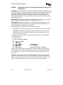
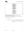
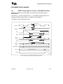
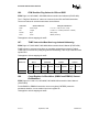
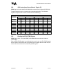
8XC196NP SPECIFICATION UPDATE Release Date: September, 1996 Order Number 272838-002 The 8XC196NP may contain design defects or errors known as errata. Characterized errata that may cause the 8XC196NP’s behavior to deviate from published specifications are documented in this specification update. 8XC196NP SPECIFICATION UPDATE Information in this document is provided in connection with Intel products. No license, express or implied, by estoppel or otherwise, to any intellectual property rights is granted by this document. Except as provided in Intel’s Terms and Conditions of Sale for such products, Intel assumes no liability whatsoever, and Intel disclaims any express or implied warranty, relating to sale and/or use of Intel products including liability or warranties relating to fitness for a particular purpose, merchantability, or infringement of any patent, copyright or other intellectual property right. Intel products are not intended for use in medical, life saving, or life sustaining applications. Intel may make changes to specifications and product descriptions at any time, without notice. The 8XC196NP may contain design defects or errors known as errata. Current characterized errata are available on request. Contact your local Intel sales office or your distributor to obtain the latest specifications before placing your product order. * Third-party brands and names are the property of their respective owners. Copies of documents which have an ordering number and are referenced in this document, or other Intel literature, may be obtained from: Intel Corporation P.O. Box 7641 Mt. Prospect, IL 60056-7641 or call in North America 1-800-879-4683, Europe 44-0-1793-431-155, France 44-0-1793-421-777, Germany 44-0-1793-421-333 other Countries 708-296-9333 Copyright 1996, Intel Corporation ii September, 1996 272838-002 8XC196NP SPECIFICATION UPDATE CONTENTS REVISION HISTORY ............................................................................... 1 PREFACE ................................................................................................ 2 SUMMARY TABLE OF CHANGES ......................................................... 3 IDENTIFICATION INFORMATION........................................................... 5 ERRATA .................................................................................................. 5 SPECIFICATION CHANGES................................................................... 7 SPECIFICATION CLARIFICATIONS..................................................... 10 DOCUMENTATION CHANGES............................................................. 13 272838-002 September, 1996 iii 8XC196NP SPECIFICATION UPDATE REVISION HISTORY Date of Revision Version 07/01/96 001 This is the new Specification Update document. It contains all identified errata published prior to this date. Description 09/06/96 002 Added erratum number 9600005, “Altering the Chip-select Configuration While Executing from the Same Region.” Clarified problem statements in errata numbers 9600001 and 9600003. 272838-002 September, 1996 1 of 17 8XC196NP SPECIFICATION UPDATE PREFACE As of July, 1996, Intel’s Semiconductor Products Group has consolidated available historical device and documentation errata into this new document type called the Specification Update. We have endeavored to include all documented errata in the consolidation process; however, we make no representations or warranties concerning the completeness of the Specification Update. This document is an update to the specifications contained in the Affected Documents/ Related Documents table below.This document is a compilation of device and documentation errata, specification clarifications and changes. It is intended for hardware system manufacturers and software developers of applications, operating systems, or tools. Information types defined in Nomenclature are consolidated into the specification update and are no longer published in other documents. This document may also contain additional information that was not previously published. Affected Documents/Related Documents Title 8XC196NP Commercial CHMOS 16-bit Microcontroller datasheet 8XC196NP, 80C196NU Microcontroller User’s Manual Order 272459-004 272479-002 Nomenclature Errata are design defects or errors. These may cause the published (component, board, system) behavior to deviate from published specifications. Hardware and software designed to be used with any component, board, and system must consider all errata documented. Specification Changes are modifications to the current published specifications. These changes will be incorporated in any new release of the specification. Specification Clarifications describe a specification in greater detail or further highlight a specification’s impact to a complex design situation. These clarifications will be incorporated in any new release of the specification. Documentation Changes include typos, errors, or omissions from the current published specifications. These changes will be incorporated in any new release of the specification. 2 of 17 September, 1996 272838-002 8XC196NP SPECIFICATION UPDATE NOTE: Errata remain in the specification update throughout the product’s lifecycle, or until a particular stepping is no longer commercially available. Under these circumstances, errata removed from the specification update are archived and available upon request. Specification changes, specification clarifications and documentation changes are removed from the specification update when the appropriate changes are made to the appropriate product specification or user documentation (datasheets, manuals, etc.). SUMMARY TABLE OF CHANGES The following table indicates the errata, specification changes, specification clarifications, or documentation changes which apply 8XC196NP product. Intel may fix some of the errata in a future stepping of the component, and account for the other outstanding issues through documentation or specification changes as noted. This table uses the following notations: Codes Used in Summary Table Steps X: (No mark) or (Blank box): Errata exists in the stepping indicated. Specification Change or Clarification that applies to this stepping. This erratum is fixed in listed stepping or specification change does not apply to listed stepping. Page (Page): Page location of item in this document. Status Doc: Fix: Fixed: NoFix: Eval: Document change or update will be implemented. This erratum is intended to be fixed in a future step of the component. This erratum has been previously fixed. There are no plans to fix this erratum. Plans to fix this erratum are under evaluation. Row Change bar to left of table row indicates this erratum is either new or modified from the previous version of the document. 272838-002 September, 1996 3 of 17 8XC196NP SPECIFICATION UPDATE Errata No. Steppings A Page Status ERRATA B 9600001 X 5 Fixed Illegal Opcode Interrupt Vector in 1-Mbyte Mode 9600002 X 5 Fixed Aborted Interrupt Vector to Low Priority Interrupt in 1Mbyte Mode 9600003 X 6 Fixed PTS Request During Interrupt Latency in 1-Mbyte Mode 9600004 X X 7 NoFix Jump Instructions at 64K Page Boundary 9600005 X X 8 NoFix Altering the Chip-select Configuration While Executing in the Same Region Specification Changes No. Steppings # Page # Status SPECIFICATION CHANGES # None for this revision of this specification update. Specification Clarifications No. Steppings Page SPECIFICATION CLARIFICATIONS A B 001 X X 10 BREQ# Signal 002 X X 10 HLDA# Signal 003 X X 10 HOLD# Signal 004 X X 10 Indirect Addressing with Autoincrement 005 X X 12 Reserved Memory Locations Documentation Changes No. Doc Rev Page DOCUMENTATION CHANGES 001 004 13 READY Timing Diagram Correction- 8XC196NP Datasheet Errata 002 002 14 Indirect Addressing With the Stack Pointer 003 002 15 Stack Operation 004 002 15 Serial Port Control and Status Registers 005 002 15 External Memory Interface Signals 006 002 15 PSW Overflow Flag Values for DIV and DIVB 007 002 16 TIJMP Instruction Must Use Long-Indexed Addressing 008 002 16 Count Register for Block Move (BMOVI and EBMOVI) Cannot Be Windowed 009 002 17 Shift Instructions (User’s Manual, Page A-59) 010 002 17 Reading the EPA_PEND Register 4 of 17 September, 1996 272838-002 8XC196NP SPECIFICATION UPDATE IDENTIFICATION INFORMATION Markings A-step denoted by “A” at the end of the topside tracking number B-step denoted by “B” or “C” at the end of the topside tracking number ERRATA 9600001. Illegal Opcode Interrupt Vector in 1-Mbyte Mode PROBLEM: The illegal opcode interrupt should be generated when there is an attempt to execute an undefined opcode, and should vector to address FF2012H to handle the interrupt. But in 1-Mbyte mode only, the vector address for the illegal opcode interrupt is not generated correctly and a random vector address is generated. IMPLICATION: Code that executes an illegal opcode (10h or E5h) will vector to a random address. WORKAROUND: Use a C-compiler or Assembler that will flag the Illegal opcode or put a reset opcode (FFh) at the end of any data tables or unused memory locations. STATUS: Refer to Summary Table of Changes to determine the affected stepping(s). 9600002. Aborted Interrupt Vectors to Lowest Priority Interrupt in 1-Mbyte Mode PROBLEM: In 1-Mbyte mode only, an aborted interrupt (either intentional or unintentional) may cause an undesired branch to the lowest-priority interrupt vector (FF2000H) even if the lowest-priority interrupt is masked. This may occur if any bit in the INT_MASK, INT_MASK1, INT_PEND, or INT_PEND1 register is cleared after the corresponding INT_PEND or INT_PEND1 bit is set. Example: If the EXTINT0 interrupt on the 8XC196NP is enabled by setting INT_MASK.3, and a rising edge on EXTINT0 occurs, INT_PEND.3 is then set. The following instruction may cause the CPU to vector to 0FF2000H instead of 0FF2006H. !.$" ).4?-!3+ &( MASKS %84).4 MAY CAUSE VECTOR TO &&( IMPLICATION: This may occur if any bit in the INT_MASK, INT_MASK1, INT_PEND, or INT_PEND1 register is cleared after the corresponding INT_PEND or INT_PEND1 bit is set. An undesired branch to the lowest priority interrupt may occur if an interrupt is aborted, unless the workaround is used. 272838-002 September, 1996 5 of 17 8XC196NP SPECIFICATION UPDATE WORKAROUND: Use a disable interrupt (DI) instruction before clearing a bit in INT_MASK, INT_MASK1, INT_PEND, or INT_PEND1. The following code example demonstrates how to safely disable the EXTINT0 interrupt. $) !.$" %) ).4?-!3+ &( DISABLE INTERRUPTS MASK %84).4 ENABLE INTERRUPTS STATUS: Refer to Summary Table of Changes to determine the affected stepping(s). 9600003. PTS Request During Interrupt Latency in 1-Mbyte Mode PROBLEM: This erratum occurs only in 1-Mbyte mode. If a standard interrupt occurs at approximately the same time (this time is code dependent and therefore cannot be stated as an exact number of state times) as a PTS serviced interrupt, the PTS interrupt may be processed as a standard interrupt. The standard interrupt service routine for a PTS serviced interrupt (usually referred to as the End-of-PTS) is typically used to modify the PTS control block and re-enable the PTS by setting the corresponding bit in the PTSSEL register. When this anomaly occurs, the End-of-PTS service routine will execute regardless of the value in PTSCOUNT. As a result, an undetermined number of PTS cycles will be missed. This applies to all interrupts serviced by the PTS. IMPLICATION: Those customers using the PTS and standard interrupts are affected. If the workaround described below is not used, an undetermined number of PTS cycles may be missed. WORKAROUND: In the standard interrupt service routine (End-of-PTS) for each PTS enabled, the first instruction following a PUSHF or PUSHA should determine whether the associated bit in the PTSSEL register is set or cleared. Checking this bit will determine whether the desired number of cycles were completed or a premature End-of-PTS occurred. If the bit is set, the associated pending bit in the INT_PEND or INT_PEND1 should be set, followed by a RET statement. This will cause a PTS cycle to occur. If the associated bit in the PTSSEL register is cleared, the normal End-of-PTS procedure should be executed. 6 of 17 September, 1996 272838-002 8XC196NP SPECIFICATION UPDATE The following is an example of an End-of-PTS service routine for external interrupt 0 (EXTINT0). #3%' !4 &&( $#7 %84).4?%.$?/&?043 #3%' !4 &&( %84).4?%.$?/&?043 053(! *"# 0433%, /+!9 /2" ).4?0%.$ ( 0/0! 2%4 /+!9 RELOAD 043#/5.4 RE ENABLE 0433%, 0/0! 2%4 STATUS: Refer to Summary Table of Changes to determine the affected stepping(s). 9600004. Jump Instructions at a 64K Boundary PROBLEM: Any jump, conditional jump, or call instruction located within six bytes of the top of any 64K page boundary (e.g., 01FFFAH-01FFFFH) may cause a jump to the wrong page. When a jump instruction with a negative offset lies across a page boundary (instruction begins on one page, executes on next page, and jumps back to first page), the page number is decremented one page too many. Example: Current instruction code fetch crosses from page F1xxxxH to F2xxxxH and executes a short jump back to page F1xxxxH. The error causes the jump to go to page F0xxxxH. IMPLICATION: SJMP, LJMP, SCALL, LCALL, and conditional jump instructions located near a page boundary will not function properly. WORKAROUND: To ensure that this problem does not occur, place at least six NOPs at the top of each page. STATUS: Refer to Summary Table of Changes to determine the affected stepping(s). 272838-002 September, 1996 7 of 17 8XC196NP SPECIFICATION UPDATE 9600005. Altering the Chip-select Configuration While Executing in the Same Region PROBLEM: The 8XC196NP does not support changing a chip-select configuration while code is executing in the memory region that is selected by that chip select. Programming the CSx# configuration registers while code is executing from the memory device selected by the CSx# pin causes unpredictable behavior of the CSx# output pin. For CS0#, this problem also occurs at reset because CS0# is activated to read instructions immediately after reset. IMPLICATION: An attempt to modify the configuration of the currently active chip-select region may result in unpredictable behavior of the CSx# output pin. WORKAROUND: Refer to the Chapter 13, “Interfacing with External Memory,” in the 8XC196NP, 80C196NU Microcontroller User’s Manual (Order No 272479-002) for a detailed description of configuring the chip-selects. Code that configures a chip select must write to three registers: • ADDRCOMx, the address compare register, which determines the start of a region • ADDRMSKx, the address mask register, which determines the size of the region • BUSCONx, the bus control register, which determines the characteristics of the memory device in the region For example, the following code excerpt sets up CS0# so that it is active for address region E000–F000H: SET UP #3 TMP IS A SCRATCH REGISTER ST ZERO?REG ADDRMSK LD ST ST LDB STB TMP TMP TMP TMP TMP EH ADDRCOM ADDRMSK CH BUSCON ADDRESS %H RANGE % &H DEMUXED BITS WAIT STATES When the microcontroller tries to execute this code after a reset, the CS0# output is unpredictable because CS0# is automatically activated to read instructions when the microcontroller comes out of reset. This code alters the chip-select registers for the active region. A safe way to set up CSx#, even when executing code in that region, is to force the CSx# pin to its active state. To do so, configure CSx# (P3.x) as a general-purpose I/O signal to output a logical zero while software configures the chip-select. After the chipselect is configured, reconfigure the signal as a special-function signal (CSx#). 8 of 17 September, 1996 272838-002 8XC196NP SPECIFICATION UPDATE The following code excerpt adds instructions to force P3.0 low while the chip-select configuration takes place, then reconfigure the pin as CS0#. GENERATE A ØFAKEÙ #3 ACTIVE ANDB P?DIR?E ./4 CONFIGURE 0 AS COMPLEMENTARY OUTPUT ANDB P?REG?E ./4 CONFIGURE 0 TO DRIVE ANDB P?MODE?E ./4 CONFIGURE 0 AS GENERAL PURPOSE )/ SET UP #3 TMP IS A SCRATCH REGISTER ST ZERO?REG ADDRMSK LD ST ST LDB STB TMP TMP TMP TMP TMP EH ADDRCOM ADDRMSK CH BUSCON ADDRESS %H RANGE % &H DEMUXED BITS WAIT STATES RESTORE #3 CONTROL OVER THE 0#3 PIN ORB P?MODE?E CONFIGURE 0 AS SPECIAL FUNCTION #3 This same method can be used for any chip-select output. STATUS: Refer to Summary Table of Changes to determine the affected stepping(s). SPECIFICATION CHANGES None for this revision of this specification update. 272838-002 September, 1996 9 of 17 8XC196NP SPECIFICATION UPDATE SPECIFICATION CLARIFICATIONS 001. BREQ# Signal PROBLEM: This active-low output signal is asserted during a hold cycle when the bus controller has a pending external memory cycle. When the bus-hold protocol is enabled (WSR.7 is set), the P2.3/BREQ# pin can function only as BREQ#, regardless of the configuration selected through the port configuration registers (P2_MODE, P2_DIR, and P2_REG). An attempt to change the pin configuration is ignored until the bus-hold protocol is disabled (WSR.7 is cleared). 002. HLDA# Signal PROBLEM: This active-low output indicates that the CPU has released the bus as the result of an external device asserting HOLD#. When the bus-hold protocol is enabled (WSR.7 is set), the P2.6/HLDA# pin can function only as HLDA#, regardless of the configuration selected through the port configuration registers (P2_MODE, P2_DIR, P2_REG). An attempt to change the pin configuration is ignored until the bus-hold protocol is disabled (WSR.7 is cleared). 003. HOLD# Signal PROBLEM: An external device uses this active-low input signal to request control of the bus. When the bus-hold protocol is enabled (WSR.7 is set), the P2.5/HOLD# pin can function only as HOLD#, regardless of the configuration selected through the port configuration registers (P2_MODE, P2_DIR, P2_REG). An attempt to change the pin configuration is ignored until the bus-hold protocol is disabled (WSR.7 is cleared). 004. Indirect Addressing with Autoincrement PROBLEM: For indirect addressing with autoincrement, a pointer that points to itself results in an access to the incremented pointer address rather than the original pointer address. The CPU stores the pointer’s value in a temporary register, increments the pointer, then accesses the operand at the address contained in the temporary register, as shown in this flowchart. 10 of 17 September, 1996 272838-002 8XC196NP SPECIFICATION UPDATE Get Indirect Address Pointer Copy Indirect Address Pointer to Temporary Register Increment Indirect Address Pointer Get Operand from Address in Temporary Register Continue Execution of Instruction A4378-01 Therefore, if the pointer points to itself, the CPU accesses the operand at the incremented address contained in the pointer. For example, assume ax = 1CH and bx = 40H. The following code causes the CPU to access the operand at the incremented address: LD LDB AX AX BX ;AX= LD LDB #( #( ( ;#(= 272838-002 #( ← #( LOAD LOCATION #( WITH VALUE #( TEMP ← #( SAVE #( INTO TEMP REGISTER #( ← $( INCREMENT THE CONTENTS OF #( ( ← $( LOAD THE CONTENTS OF LOCATION #( LOCATION #( NOW CONTAINS THE VALUE $( INTO ( September, 1996 11 of 17 8XC196NP SPECIFICATION UPDATE 005. Reserved Memory Locations PROBLEM: Reserved memory locations on the 8XC196NP should not be used by the user’s code. While many are reserved for future use, others are used internally by Intel. The values in reserved memory are subject to change without notice and therefore should not be used as a reference of any kind. 12 of 17 September, 1996 272838-002 8XC196NP SPECIFICATION UPDATE DOCUMENTATION CHANGES 001. READY Timing Diagram Correction - 8XC196NP Data Sheet ITEM: 8XC196NP Commercial CHMOS 16-bit Microcontroller datasheet (Order #272459-004) The value 2T 1 was incorrectly shown as T 1 in the READY timing diagrams. The following two figures replace Figure 7 and Figure 9 in the datasheet. XTAL XTAL This applies to silicon steppings A and B. TCLYX (max) CLKOUT TAVYV TCLYX (min) READY TLHLH + 2TXTAL1 ALE TRLRH + 2TXTAL1 RD# AD15:0 (read) TRLDV + 2TXTAL1 TAVDV + 2TXTAL1 Address Out Data In TWLWH + 2TXTAL1 WR# TQVWH + 2TXTAL1 AD15:0 (write) Address Out Data Out BHE#, INST A19:16 Extended Address Out CSx# A3250-01 Figure 7. READY Timing Diagram (Multiplexed Bus Mode) 272838-002 September, 1996 13 of 17 8XC196NP SPECIFICATION UPDATE TCLYX (max) CLKOUT TAVYV TCLYX (min) READY TLHLH + 2TXTAL1 ALE TRLRH + 2TXTAL1 RD# TRLDV + 2TXTAL1 TAVDV + 2TXTAL1 AD15:0 (read) Data TWLWH + 2TXTAL1 WR# TQVWH + 2TXTAL1 AD15:0 (write) Data Out BHE#, INST A19:0 Extended Address Out CSx# A3256-01 Figure 9. READY Timing Diagram (Demultiplexed Bus Mode) 002. Indirect Addressing With the Stack Pointer ITEM: Page 4-9, 8XC196NP, 80C196NU Microcontroller User’s Manual (272479-002) The explanatory comments for the PUSH [SP] instruction are incorrect. The stack pointer is decremented by 2, not incremented by 2 in this instruction. The correct text is as follows: 053( ;30= DUPLICATE TOP OF STACK 30 ← 30Ó This applies to silicon steppings A and B. 14 of 17 September, 1996 272838-002 8XC196NP SPECIFICATION UPDATE 003. Stack Operation ITEM: Page 4-13, 8XC196NP, 80C196NU Microcontroller User’s Manual (272479-002) The stack order shows the low word of param2 pushed onto the stack before the high word. This is reversed. The correct stack order is as follows: PARAM HIGH WORD OF PARAM LOW WORD OF PARAM UNDEFINEDPARAM RETURN ADDRESS ← STACK POINTER This applies to silicon steppings A and B. 004. Serial Port Control and Status Registers ITEM: Page 8-2, 8XC196NP, 80C196NU Microcontroller User’s Manual (272479-002) In Table 8-2, the fields that describe programming of P1_DIR and P2_DIR are incorrect. The correct text is as follows: P1_DIR This register selects the direction of each port 1 pin. To use T1CLK as the input clock to the baud-rate generator, set P1_DIR.4. P2_DIR This register selects the direction of each port 2 pin. Set P2_DIR.1 to configure RXD (P2.1) as a high-impedance input/open-drain output, and clear P2_DIR.0 to configure TXD (P2.0) as a complementary output. This applies to silicon steppings A and B. 005. External Memory Interface Signals ITEM: Pages 13-3 and 13-5, 8XC196NP, 80C196NU Microcontroller User’s Manual (272479-002) In Table 13-2, the “Multiplexed With” column contains incorrect information for the BHE# and WRH# signals. The BHE# and WRH# signals are multiplexed with one another, but are not multiplexed with P5.5. (The 8XC196NP and 80C196NU have no port 5.) For the BHE# signal, the “multiplexed with” column should contain only WRH#. For the WRH# signal, the “multiplexed with” column should contain only BHE#. This applies to silicon steppings A and B. 272838-002 September, 1996 15 of 17 8XC196NP SPECIFICATION UPDATE 006. PSW Overflow Flag Values for DIV and DIVB ITEM: Page A-4, 8XC196NP, 80C196NU Microcontroller User’s Manual (272479-002) The “V Flag Set if Quotient Is” values are incorrect for the DIV and DIVB instructions. The correct values for all divide instructions are as follows: Instruction Quotient Stored in: V Flag Set if Quotient is: DIVB Short Integer < -127 or > +128 (<81 H or > 80H) DIV Integer < -32767 or > +32768 (< 8001H or > 8000H) DIVUB Byte >255 (>FFH) DIVU Word >65535 (>FFFFH) This applies to silicon steppings A and B. 007. TIJMP Instruction Must Use Long-Indexed Addressing ITEM: Page A-57, 8XC196NP, 80C196NU Microcontroller User’s Manual (272479-002) TIJMP cannot be executed using direct or immediate addressing as stated in Table 8. TIJMP can be executed only using long-indexed addressing; it is a 4-byte instruction with opcode E2H. This applies to silicon steppings A and B. Mnemonic Direct Length TIJMP 008. ---- Immediate Opcode ---- Length ---- Opcode ---- Indirect Length ---- Opcode ---- Indexed Length S/L Opcode ----/4 E2 Count Register for Block Move (BMOVI and EBMOVI) Cannot Be Windowed ITEM: Pages A-10 and A-16, 8XC196NP, 80C196NU Microcontroller User’s Manual (272479-002) For the BMOVI or EBMOVI instruction, the count register (CNTREG) cannot be windowed; therefore, it must reside in the lower register file. This applies to silicon steppings A and B. 16 of 17 September, 1996 272838-002 8XC196NP SPECIFICATION UPDATE 009. Shift Instructions (User’s Manual, Page A-59) ITEM: Page A-59, 8XC196NP, 80C196NU Microcontroller User’s Manual (272479-002) The shift instructions can be executed using immediate addressing. The instruction lengths and opcodes are the same as those for direct addressing. Shift Mnemonic Direct Length Opcode Immediate Length Opcode Indirect Length Opcode Indexed Length Opcode NORML 3 0F 3 0F ---- ---- ---- ---- SHL 3 09 3 09 ---- ---- ---- ---- SHLB 3 19 3 19 ---- ---- ---- ---- SHLL 3 0D 3 0D ---- ---- ---- ---- SHR 3 08 3 08 ---- ---- ---- ---- SHRA 3 0A 3 0A ---- ---- ---- ---- SHRAB 3 1A 3 1A ---- ---- ---- ---- SHRAL 3 0E 3 0E ---- ---- ---- ---- SHRB 3 18 3 18 ---- ---- ---- ---- SHRL 3 0C 3 0C ---- ---- ---- ---- 010. Reading the EPA_PEND Register ITEM: Pages 10-22, 10-23, 8XC196NP, 80C196NU Microcontroller User’s Manual (272479-002) After the EPA_PEND register is read directly by the user’s code, the EPA_PEND register bits are cleared. If these bits need to be preserved for use again after the initial read, the user’s code must save the value of the EPA_PEND register. 272838-002 September, 1996 17 of 17