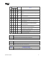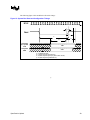
1
Mobile Intel® Celeron® Processor on
.13 Micron Process in Micro-FCPGA
Package
Specification Update
October 2005
Notice: The mobile Intel® Celeron® processor may contain design defects or errors known as
errata which may cause the product to deviate from published specifications. Current
characterized errata are documented in this Specification Update.
Document Number: 251309-028
R
INFORMATION IN THIS DOCUMENT IS PROVIDED IN CONNECTION WITH INTEL® PRODUCTS. NO LICENSE, EXPRESS OR IMPLIED, BY
ESTOPPEL OR OTHERWISE, TO ANY INTELLECTUAL PROPERTY RIGHTS IS GRANTED BY THIS DOCUMENT. EXCEPT AS PROVIDED IN
INTEL’S TERMS AND CONDITIONS OF SALE FOR SUCH PRODUCTS, INTEL ASSUMES NO LIABILITY WHATSOEVER, AND INTEL DISCLAIMS
ANY EXPRESS OR IMPLIED WARRANTY, RELATING TO SALE AND/OR USE OF INTEL PRODUCTS INCLUDING LIABILITY OR WARRANTIES
RELATING TO FITNESS FOR PARTICULAR PURPOSE, MERCHANTABILITY OR INFRINGEMENT OR ANY PATENT, COPYRIGHT OR OTHER
INTELLECTUAL PROPERTY RIGHT. Intel products are not intended for use in medical, life saving, or life sustaining applications.
Intel may make changes to specifications and product descriptions at any time, without notice.
Designers must not rely on the absence or characteristics of any features or instructions marked “reserved” or “undefined.” Intel reserves these for future
definition and shall have no responsibility whatsoever for conflicts or incompatibilities arising from future changes to them.
The Mobile Intel® Celeron® processor may contain design defects or errors known as errata which may cause the product to deviate from published
specifications. Current characterized errata are available on request.
†
Hyper-Threading Technology requires a computer system with a Mobile Intel Pentium 4 Processor, a chipset and BIOS that utilize this technology, and an
operating system that includes optimizations for this technology. Performance will vary depending on the specific hardware and software you use. See
http://www.intel.com/info/hyperthreading for information.
Contact your local Intel sales office or your distributor to obtain the latest specifications and before placing your product order.
Intel, Pentium, Celeron, Intel Xeon, Intel SpeedStep, Intel NetBurst and the Intel logo are trademarks or registered trademarks of Intel Corporation or its
subsidiaries in the United States and other countries.
*Other names and brands may be claimed as the property of others.
Copyright © Intel Corporation 2002-2005. All rights reserved.
2
Specification Update
R
Contents
Revision History............................................................................................................................4
Preface .........................................................................................................................................6
Summary of Changes...................................................................................................................8
Identification Information ............................................................................................................12
Errata ..........................................................................................................................................15
Specification Clarifications..........................................................................................................34
Specification Changes................................................................................................................37
Documentation Changes ............................................................................................................40
Specification Update
3
R
Revision History
Revision
Number
4
Description
Date
-001
Initial Release
June 2002
-002
Updated Identification Information table.
August 2002
-003
Updated Documentation Change summary by removing old items that
have been incorporated into the Software Developer’s Manual; Added
errata V30-V32; Added Documentation Changes V3-V24.
September 2002
-004
Updated Summary of Changes; Added prefix letter W; Removed
previous errata V32 as not applicable, added new errata V32; Added
Documentation Changes V25-V32.
October 2002
-005
Added errata V33; Added Spec Clarification V1; Added Spec Change V1;
Removed Documentation Changes that have been incorporated into the
Software Developer’s Manual; Added a note in Documentation Changes.
November 2002
-006
No new Errata, Documentation Change, Spec Clarification, or Spec
Change. Updated note concerning the Software Developer’s Manual.
December 2002
-007
Added Erratum V34. Updated summary tables to include C1 step.
January 2003
-008
Added Erratum V35.
February 2003
-009
Updated Erratum V34, added new Erratum V36
March 2003
-010
Updated codes used in summary tables. Updated errata summary table
entry for V27, V28, V34, & V36. Updated tables for D1-step
April 2003
-011
Added info for C-1 step 1.6 GHz to 2.2 GHz to Table 1.
May 2003
-012
Updated Erratum V33. Added identification info for D-1 step 2.4 GHz.
Updated summary table code Z.
June 2003
-013
Added Erratum V37.
July 2003
-014
Added V2 Specification Change. Added Errata V38.
August 2003
-015
Added Errata V39 and V40.
September 2003
-016
Added Errata V41.
October 2003
-017
Updated Errata V41.
November 2003
-018
Updated Errata V42.
March 2004
-019
Updated Errata V6.
April 2004
-020
Updated Errata V11. Added Errata V43.
May 2004
-021
Added Errata V44. Updated Processor Identification Information
June 2004
-022
Added Errata V45.
September 2004
-023
Added Errata V46-47
October 2004
-024
Added errata V48
November 2004
-025
Added errata V49
December 2004
-026
Added Specification Clarification V2
May 2005
Specification Update
R
-027
Updated Related Documents table
July 2005
-028
Added errata V50 and updated Processor Identification Table.
October 2005
Specification Update
5
R
Preface
This document is an update to the specifications contained in the document listed in the following
Affected/Related Documents table. It is a compilation of device and document errata and specification
clarifications and changes, and is intended for hardware system manufacturers and for software
developers of applications, operating system, and tools.
Information types defined in the Nomenclature section of this document are consolidated into this update
document and are no longer published in other documents. This document may also contain information
that has not been previously published.
Affected Documents
Document Title
®
®
Mobile Intel Celeron Processor on .13 Micron Process in MicroFCPGA Package Datasheet
Document Number
251308
Related Documents
Document Title
®
253665
®
253666
®
253667
®
253668
IA-32 Intel Architecture Software Developer's Manual, Volume 1:
Basic Architecture
IA-32 Intel Architecture Software Developer's Manual, Volume
2A: Instruction Set Reference, A-M
IA-32 Intel Architecture Software Developer's Manual, Volume
2B: Instruction Set Reference, N-Z
IA-32 Intel Architecture Software Developer's Manual, Volume 3:
System Programming Guide
6
Document Number
Specification Update
R
Nomenclature
S-Spec Number is a five-digit code used to identify products. Products are differentiated by their unique
characteristics, e.g., core speed, L2 cache size, package type, etc. as described in the processor
identification information table. Care should be taken to read all notes associated with each S-Spec
number.
Errata are design defects or errors. Errata may cause the mobile Intel Pentium 4 processor-m’s behavior
to deviate from published specifications. Hardware and software designed to be used with any given
processor must assume that all errata documented for that processor are present on all devices unless
otherwise noted.
Documentation Changes include typos, errors, or omissions from the current published specifications.
These changes will be incorporated in the next release of the specifications.
Specification Clarifications describe a specification in greater detail or further highlight a
specification’s impact to a complex design situation. These clarifications will be incorporated in the next
release of the specifications.
Specification Changes are modifications to the current published specifications for the Intel Pentium 4
processor. These changes will be incorporated in the next release of the specifications.
Specification Update
7
R
Summary of Changes
The following table indicates the Errata, Documentation Changes, Specification Clarifications, or
Specification Changes that apply to Intel Pentium 4 processors. Intel intends to fix some of the errata in
a future stepping of the component, and to account for the other outstanding issues through
documentation or specification changes as noted. This table uses the following notations:
Codes Used in Summary Table
Stepping
X:
Erratum, Specification Change or Clarification that applies to this stepping.
(No mark) or (Blank Box): This erratum is fixed in listed stepping or specification change does not
apply to listed stepping.
Status
Doc:
Document change or update that will be implemented.
PlanFix:
This erratum may be fixed in a future of the product.
Fixed:
This erratum has been previously fixed.
NoFix:
There are no plans to fix this erratum.
PKG:
This column refers to errata on the Mobile Intel® Celeron® Processor on .13
Micron Process in Micro-FCPGA Package substrate.
AP:
APIC related erratum.
Shaded:
This item is either new or modified from the previous version of the
document.
Each Specification Update item is prefixed with a capital letter to distinguish the product. The key
below details the letters that are used in Intel’s microprocessor Specification Updates:
A = Intel ® Pentium ® II processor
B = Mobile Intel ® Pentium ® II processor
C = Intel ® Celeron ® processor
E = Intel ® Pentium ® III processor
F = Intel® Pentium® processor Extreme Edition and Intel® Pentium® D processor
G = Intel ® Pentium ® III Xeon™ processor
H = Mobile Intel ® Celeron ® processor at 466/433/400/366/333/300 and 266 MHz
J = 64-bit Intel® Xeon™ processor MP with 1MB L2 Cache
K = Mobile Intel ® Pentium ® III processor
8
Specification Update
R
L = Intel ® Celeron ® D processor
M = Mobile Intel ® Celeron ® processor
N = Intel ® Pentium ® 4 processor
O = Intel ® Xeon™ processor MP
P = Intel ® Xeon™ processor
Q = Mobile Intel® Pentium® 4 processor supporting Hyper-Threading Technology on 90-nm process
technology
R = Intel® Pentium® 4 processor on 90 nm process
S = 64-bit Intel® Xeon™ processor with 800 MHz system bus (1 MB and 2 MB L2 cache versions)
T = Mobile Intel® Pentium® 4 processor-M
V = Mobile Intel® Celeron® processor on .13 Micron Process in Micro-FCPGA Package
W= Intel® Celeron® M processor
X = Intel® Pentium® M processor on 90nm process with 2-MB L2 Cache
Y = Intel® Pentium® M processor
Z = Mobile Intel ® Pentium ® 4 processor with 533 MHz system bus
AC = Intel® Celeron® Processor in 478 Pin Package
The Specification Updates for the Pentium® processor, Pentium® Pro processor, and other Intel products
do not use this convention
Steppings
NO.
Plans
B0
C1
ERRATA
D1
V1
X
X
X
NoFix
I/O restart in SMM may fail after simultaneous machine check
exception (MCE)
V2
X
X
X
NoFix
MCA registers may contain invalid information if RESET# occurs and
PWRGOOD is not held asserted
V3
X
X
X
NoFix
Transaction is not retried after BINIT#
V4
X
X
X
NoFix
Invalid opcode 0FFFh requires a ModRM byte
V5
X
X
X
NoFix
FSW may not be completely restored after page fault on FRSTOR or
FLDENV instructions
V6
X
X
X
NoFix
The Processor Signals Page-Fault Exception (#PF) Instead of
Alignment Check Exception (#AC) on an Unlocked CMPXCHG8B
Instruction
V7
X
X
X
NoFix
When in no-fill mode the memory type of large pages are incorrectly
forced to uncacheable
V8
X
X
X
NoFix
Processor may hang due to speculative page walks to non-existent
system memory
V9
X
X
X
NoFix
The IA32_MC1_STATUS register may contain incorrect information for
correctable errors
V10
X
X
X
NoFix
Debug mechanisms may not function as expected
V11
X
X
X
NoFix
Machine check architecture error reporting and recovery may not work
as expected
V12
X
X
X
NoFix
Cascading of performance counters does not work correctly when
forced overflow is enabled
V13
X
X
X
NoFix
EMON event counting of x87 loads may not work as expected
V14
X
X
X
NoFix
Speculative page fault may cause livelock
Specification Update
9
R
Steppings
NO.
Plans
B0
V15
X
V16
X
V17
X
C1
X
X
V18
V19
X
X
X
Fixed
Incorrect data may be returned when page tables are in Write
Combining (WC) memory space
NoFix
Processor issues inconsistent transaction size attributes for locked
operation
Fixed
Multiple accesses to the same S-state L2 cache line and ECC error
combination may result in loss of cache coherency
Fixed
Processor may hang when resuming from Deep Sleep state
NoFix
When the processor is in the System Management Mode (SMM),
debug registers may be fully writeable
V20
X
X
X
NoFix
Associated counting logic must be configured when using Event
Selection Control (ESCR) MSR
V21
X
X
X
NoFix
IA32_MC0_ADDR and IA32_MC0_MISC Registers Will Contain
Invalid or Stale Data Following a Data, Address, or Response Parity
Error
V22
X
Fixed
CR2 May Be Incorrect or an Incorrect Page Fault Error Code May Be
Pushed Onto Stack After Execution of an LSS Instruction
V23
X
Fixed
BPM[5:3]# and GHI# VIL Do Not Meet Specification
V24
X
NoFix
Processor May Hang Under Certain Frequencies and 12.5%
STPCLK# Duty Cycle
V25
X
NoFix
System May Hang if a Fatal Cache Error Causes Bus Write Line
(BWL) Transaction to Occur to the Same Cache Line Address as an
Outstanding Bus Read Line (BRL) or Bus Read-Invalidate Line (BRIL)
V26
X
Fixed
L2 Cache May Contain Stale Data in the Exclusive State
V27
X
Fixed
Re-mapping the APIC Base Address to a Value Less Than or Equal to
0xDC001000 may Cause IO and Special Cycle Failure
V28
X
Fixed
Erroneous BIST Result Found in EAX Register After Reset
V29
X
Fixed
Processor Does not Flag #GP on Non-zero Write to Certain MSRs
V30
X
X
X
NoFix
Simultaneous Assertion of A20M# and INIT# may Result in Incorrect
Data Fetch
V31
X
X
X
PlanFix
Processor Does not Respond to Break Requests From ITP
V32
X
Fixed
Processor Signature Returns Incorrect Number of ITLB Entries
V33
X
NoFix
A Write to APIC Registers Sometimes May Appear to Have Not
Occurred
Fixed
Store to Load Data Forwarding may Result in Switched Data Bytes
NoFix
Parity Error in the L1 Cache may Cause the Processor to Hang
Fixed
The TCK Input in the Test Access Port (TAP) is Sensitive to Low
Clock Edge Rates and Prone to Noise Coupling Onto TCK’s Rising or
Falling Edges
V34
10
ERRATA
D1
X
X
X
X
X
X
X
X
X
V35
X
X
V36
X
X
X
V37
X
X
X
NoFix
The State of the Resume Flag (RF Flag) in a Task-State Segment
(TSS) May be Incorrect
V38
X
X
X
NoFix
Changes to CR3 Register do not Fence Pending Instruction Page
Walks
V39
X
X
X
NoFix
System Bus Interrupt Messages without Data that Receive a
Specification Update
R
Steppings
NO.
Plans
B0
C1
ERRATA
D1
HardFailure Response May Hang the Processor
V40
X
X
X
NoFix
Memory Type of the Load Lock Different from its Corresponding Store
Unlock
V41
X
X
X
NoFix
A 16-bit Address Wrap Resulting from a Near Branch (Jump or Call)
May Cause an Incorrect Address to Be Reported to the #GP Exception
Handler
V42
X
X
X
NoFix
Incorrect Debug Exception (#DB) May Occur When a Data Breakpoint
is set on an FP Instruction
V43
X
X
X
NoFix
xAPIC May Not Report Some Illegal Vector Errors
V44
X
X
X
NoFix
Memory Aliasing of Pages as Uncacheable Memory Type and Write
Back (WB) May Hang the System
V45
X
Plan Fix
A Timing Maginality in the Arithmetic Logic Unit (ALU) May Cause
Indeterminate Behavior
V46
X
X
X
No Fix
With TF (Trap Flag) Asserted, FP Instruction That Triggers an
Unmasked FP Exception May Take Single Step Trap Before
Retirement of Instruction
V47
X
X
X
No Fix
BTS(Branch Trace Store) and PEBS(Precise Event Based Sampling)
May Update Memory outside the BTS/PEBS Buffer
V48
X
X
X
No Fix
Memory Ordering Failure May Occur with Snoop Filtering Third-Party
Agents after Issuing and Completing a BWIL (Bus Write Invalidate
Line) or BLW (Bus Locked Write) Transaction
V49
X
X
X
No Fix
Control Register 2 (CR2) Can be Updated during a REP MOVS/STOS
Instruction with Fast Strings Enabled
V50
X
X
X
No Fix
Writing the Local Vector Table (LVT) when an Interrupt is Pending May
Cause an Unexpected Interrupt
Number
SPECIFICATION CHANGE
V1
Context ID feature added to CPUID Feature/IA32_MISC_Enable Registers
V2
BR0# Maximum Hold Time Specification Change
Number
SPECIFICATION CLARIFICATIONS
®
V1
Clarifying DBI# Definition for all Processors with Intel NetBurst Microarchitecture
V2
Specification Clarification with respect to Time-stamp Counter
Number
DOCUMENTATION CHANGES
There are no Documentation Changes in this Specification Update revision.
Specification Update
11
R
Identification Information
The mobile Intel® Celeron® processor on .13 micron process in Micro-FCPGA package can be identified
by the following values:
1
Family
Model
1111
0010
2
Brand ID
3
00001000
4
5
1111
0010
00001111
NOTES:
1. The Family corresponds to bits [11:8] of the EDX register after Reset, bits [11:8] of the EAX register after the
CPUID instruction is executed with a 1 in the EAX register, and the generation field of the Device ID register
accessible through Boundary Scan.
2. The Model corresponds to bits [7:4] of the EDX register after Reset, bits [7:4] of the EAX register after the
CPUID instruction is executed with a 1 in the EAX register, and the model field of the Device ID register
accessible through Boundary Scan.
3. The Brand ID corresponds to bits [7:0] of the EBX register after the CPUID instruction is executed with a 1 in
the EAX register.
4. This brand id MUST be used in conjunction with CPUID = 0F24h.
5. This brand id MUST be used in conjunction with CPUID = 0F27h.
12
Specification Update
R
Table 1. Mobile Intel® Celeron® Processor Identification Information
S-Spec
Product
Stepping
L2
Cache
Size
(bytes)
CPU
Signature
Core Frequency
Bus
Frequency
Voltage
Package
Notes
SL6FM
B0
256 K
0F24h
1.4 GHz
400 MHz
1.3 V
Micro-FCPGA
1
SL6FN
B0
256 K
0F24h
1.5 GHz
400 MHz
1.3 V
Micro-FCPGA
1
SL6M4
C1
256 K
0F27h
1.4 GHz
400 MHz
1.3 V
Micro-FCPGA
SL6M5
C1
256 K
0F27h
1.5 GHz
400 MHz
1.3 V
Micro-FCPGA
SL6J2
C1
256 K
0F27h
1.6 GHz
400 MHz
1.3 V
Micro-FCPGA
SL6J3
C1
256 K
0F27h
1.7 GHz
400 MHz
1.3 V
Micro-FCPGA
SL6J4
C1
256 K
0F27h
1.8 GHz
400 MHz
1.3 V
Micro-FCPGA
SL6QH
C1
256 K
0F27h
2.0 GHz
400 MHz
1.3 V
Micro-FCPGA
SL6ZW
C1
256 K
0F27h
2.2 GHz
400 MHz
1.3 V
Micro-FCPGA
SL7MG
D1
256K
0F29h
1.2 GHz
400 MHz
1.3 V
Micro-FCPGA 2
SL6VG
D1
256 K
0F29h
1.70 GHz
400 MHz
1.3 V
Micro-FCPGA
SL6VH
D1
256 K
0F29h
1.80 GHz
400 MHz
1.3 V
Micro-FCPGA
SL6VJ
D1
256 K
0F29h
2.00 GHz
400 MHz
1.3 V
Micro-FCPGA
SL73Y
D1
256 K
0F29h
2.20 GHz
400 MHz
1.3 V
Micro-FCPGA
SL75J
D1
256 K
0F29h
2.40 GHz
400 MHz
1.3 V
Micro-FCPGA
NOTES:
1. Based on B0-Shrink process.
2. Supported by the Embedded Intel Architecture Division
Specification Update
13
R
Component Marking Information
®
®
Figure 1. Mobile Intel Celeron Processor on .13 Micron Process (Micro-FCPGA) Markings
FPO#
S-Spec
#
FFFFFFFF S/N
PRODUCT DETAIL
S-SPEC COO
INTEL m c ‘01
2D Matrix
(supplier Lot ID + SER#)
LEGAL REQUIREMENTS
§
14
Specification Update
R
Errata
V1.
I/O Restart in SMM may Fail after Simultaneous Machine Check Exception (MCE)
Problem:
If an I/O instruction (IN, INS, REP INS, OUT, OUTS, or REP OUTS) is being executed, and if the data
for this instruction becomes corrupted, the processor will signal a Machine Check Exception (MCE). If
the instruction is directed at a device that is powered down, the processor may also receive an assertion
of SMI#. Since MCEs have higher priority, the processor will call the MCE handler, and the SMI#
assertion will remain pending. However, upon attempting to execute the first instruction of the MCE
handler, the SMI# will be recognized and the processor will attempt to execute the SMM handler. If the
SMM handler is completed successfully, it will attempt to restart the I/O instruction, but will not have
the correct machine state, due to the call to the MCE handler.
Implication: A simultaneous MCE and SMI# assertion may occur for one of the I/O instructions above. The SMM
handler may attempt to restart such an I/O instruction, but will have an incorrect state due to the MCE
handler call, leading to failure of the restart and shutdown of the processor.
Workaround: If a system implementation must support both SMM and board I/O restart, the first thing the SMM
handler code should do is check for a pending MCE. If there is an MCE pending, the SMM handler
should immediately exit via an RSM instruction and allow the MCE handler to execute. If there is no
MCE pending, the SMM handler may proceed with its normal operation.
Status:
For the steppings affected, see the Summary Tables of Changes.
V2.
MCA Registers May Contain Invalid Information if RESET# Occurs and
PWRGOOD Is Not Held Asserted
Problem:
This erratum can occur as a result either of the following events:
•
PWRGOOD is de-asserted during a RESET# assertion causing internal glitches that may result in
the possibility that the MCA registers latch invalid information.
•
Or during a reset sequence if the processor’s power remains valid regardless of the state of
PWRGOOD, and RESET# is re-asserted before the processor has cleared the MCA registers, the
processor will begin the reset process again but may not clear these registers.
Implication: When this erratum occurs, the information in the MCA registers may not be reliable.
Workaround: Ensure that PWRGOOD remains asserted throughout any RESET# assertion and that RESET# is not reasserted while PWRGOOD is de-asserted.
Status:
For the steppings affected, see the Summary Tables of Changes.
Specification Update
15
R
V3.
Transaction Is Not Retried after BINIT#
Problem:
If the first transaction of a locked sequence receives a HITM# and DEFER# during the snoop phase it
should be retried and the locked sequence restarted. However, if BINIT# is also asserted during this
transaction, it will not be retried.
Implication: When this erratum occurs, locked transactions will unexpectedly not be retried.
Workaround: None identified
Status:
For the steppings affected, see the Summary Tables of Changes.
V4.
Invalid Opcode 0FFFh Requires a ModRM Byte
Problem:
Some invalid opcodes require a ModRM byte (or other following bytes), while others do not. The
invalid opcode 0FFFh did not require a ModRM byte in previous generation Intel architecture
processors, but does in the Intel® Pentium® 4 processor.
Implication: The use of an invalid opcode 0FFFh without the ModRM byte may result in a page or limit fault on the
Intel® Pentium® 4 processor.
Workaround: Use a ModRM byte with invalid 0FFFh opcode.
Status:
For the steppings affected, see the Summary Tables of Changes.
V5.
FSW May Not Be Completely Restored after Page Fault on FRSTOR or FLDENV
Instructions
Problem:
If the FPU operating environment or FPU state (operating environment and register stack) being loaded
by an FLDENV or FRSTOR instruction wraps around a 64Kbyte or 4Gbyte boundary and a page fault
(#PF) or segment limit fault (#GP or #SS) occurs on the instruction near the wrap boundary, the upper
byte of the FPU status word (FSW) might not be restored. If the fault handler does not restart program
execution at the faulting instruction, stale data may exist in the FSW.
Implication: When this erratum occurs, stale data will exist in the FSW.
Workaround: Ensure that the FPU operating environment and FPU state do not cross 64Kbyte or 4Gbyte boundaries.
Alternately, ensure that the page fault handler restarts program execution at the faulting instruction after
correcting the paging problem.
Status:
16
For the steppings affected, see the Summary Tables of Changes.
Specification Update
R
V6.
The Processor Signals Page-Fault Exception (#PF) Instead of Alignment Check
Exception (#AC) on an Unlocked CMPXCHG8B Instruction
Problem:
If a Page-Fault Exception (#PF) and Alignment Check Exception (#AC) both occur for an unlocked
CMPXCHG8B instruction, then #PF will be flagged.
Implication: Software that depends on the Alignment Check Exception (#AC) before the Page-Fault Exception (#PF)
will be affected since #PF is signaled in this case.
Workaround: Remove the software’s dependency on #AC having precedence over #PF. Alternately, correct the page
fault in the page fault handler and then restart the faulting instruction.
Status:
For the steppings affected, see the Summary Tables of Changes
V7.
When in No-Fill Mode the Memory Type of Large Pages are Incorrectly Forced to
Uncacheable
Problem:
When the processor is operating in No-Fill Mode (CR0.CD=1), the paging hardware incorrectly forces
the memory type of large (PSE-4M and PAE-2M) pages to uncacheable (UC) memory type regardless of
the MTRR settings. By forcing the memory type of these pages to UC, load operations, which should hit
valid data in the L1 cache, are forced to load the data from system memory. Some applications will lose
the performance advantage associated with the caching permitted by other memory types.
Implication: This erratum may result in some performance degradation when using no-fill mode with large pages.
Workaround: None identified
Status:
For the steppings affected, see the Summary Tables of Changes.
V8.
Processor May Hang Due to Speculative Page Walks to Non-Existent System
Memory
Problem:
A load operation that misses the Data Translation Lookaside Buffer (DTLB) will result in a page-walk.
If the page-walk loads the Page Directory Entry (PDE) from cacheable memory and that PDE load
returns data that points to a valid Page Table Entry (PTE) in uncacheable memory the processor will
access the address referenced by the PTE. If the address referenced does not exist the processor will
hang with no response from system memory.
Implication: Processor may hang due to speculative page walks to non-existent system memory.
Workaround: Page directories and page tables in UC memory space that are marked valid must point to physical
addresses that will return a data response to the processor.
Status:
For the steppings affected, see the Summary Tables of Changes.
Specification Update
17
R
V9.
The IA32_MC1_STATUS Register May Contain Incorrect Information for
Correctable Errors
Problem:
When a speculative load operation hits the L2 cache and receives a correctable error, the
IA32_MC1_STATUS register may be updated with incorrect information. The IA32_MC1_STATUS
register should not be updated for speculative loads.
Implication: When this erratum occurs, the IA32_MC1_STATUS register will contain incorrect information for
correctable errors.
Workaround: None identified
Status:
For the steppings affected, see the Summary Tables of Changes.
V10.
Debug Mechanisms May Not Function As Expected
Problem:
Certain debug mechanisms may not function as expected on the processor. The cases are as follows:
•
When the following conditions occur: 1) An FLD instruction signals a stack overflow or
underflow, 2) the FLD instruction splits a page-boundary or a 64 byte cache line boundary, 3) the
instruction matches a Debug Register on the high page or cache line respectively, and 4) the FLD
has a stack fault and a memory fault on a split access, the processor will only signal the stack fault
and the debug exception will not be taken.
•
When a data breakpoint is set on the ninth and/or tenth byte(s) of a floating point store using the
Extended Real data type, and an unmasked floating point exception occurs on the store, the break
point will not be captured.
•
When any instruction has multiple debug register matches, and any one of those debug registers is
enabled in DR7, all of the matches should be reported in DR6 when the processor goes to the
debug handler. This is not true during a REP instruction. As an example, during execution of a
REP MOVSW instruction the first iteration a load matches DR0 and DR2 and sets DR6 as
FFFF0FF5h. On a subsequent iteration of the instruction, a load matches only DR0. The DR6
register is expected to still contain FFFF0FF5h, but the processor will update DR6 to FFFF0FF1h.
•
A Data breakpoint that is set on a load to uncacheable memory may be ignored due to an internal
segment register access conflict. In this case the system will continue to execute instructions,
bypassing the intended breakpoint. Avoiding having instructions that access segment descriptor
registers, e.g., LGDT, LIDT close to the UC load, and avoiding serialized instructions before the
UC load will reduce the occurrence of this erratum.
Implication: Certain debug mechanisms do not function as expected on the processor.
Workaround: None identified
Status:
18
For the steppings affected, see the Summary Tables of Changes.
Specification Update
R
V11.
Machine Check Architecture Error Reporting and Recovery May Not Work As
Expected
Problem:
When the processor detects errors it should attempt to report and/or recover from the error. In the
situations described below, the processor does not report and/or recover from the error(s) as intended. When a transaction is deferred during the snoop phase and subsequently receives a Hard Failure
response, the transaction should be removed from the bus queue so that the processor may proceed.
Instead, the transaction is not properly removed from the bus queue, the bus queue is blocked, and the
processor will hang.
- When a hardware prefetch results in an uncorrectable tag error in the L2 cache,
MC0_STATUS.UNCOR and MC0_STATUS.PCC are set but no Machine Check Exception (MCE) is
signaled. No data loss or corruption occurs because the data being prefetched has not been used. If the
data location with the uncorrectable tag error is subsequently accessed, an MCE will occur. However,
upon this MCE, or any other subsequent MCE, .the information for that error will not be logged because
MC0_STATUS.UNCOR has already been set and the MCA status registers will not contain information
about the error which caused the MCE assertion but instead will contain information about the prefetch
error event.
- When the reporting of errors is disabled for Machine Check Architecture (MCA) Bank 2 by setting all
MC2_CTL register bits to 0, uncorrectable errors should be logged in the IA32_MC2_STATUS register
but no machine-check exception should be generated. Uncorrectable loads on bank 2, which would
normally be logged in the IA32_MC2_STATUS register, are not logged.
- When one half of a 64 byte instruction fetch from the L2 cache has an uncorrectable error and the other
32 byte half of the same fetch from the L2 cache has a correctable error, the processor will attempt to
correct the correctable error but cannot proceed due to the uncorrectable error. When this occurs the
processor will hang.
-When an L1 cache parity error occurs, the cache controller logic should write the physical address of
the data memory location that produced that error into the IA32_MC1_ADDR REGISTER
(MC1_ADDR). In some instances of a parity error on a load operation that hits the L1 cache, the cache
controller logic may write the physical address from a subsequent load or store operation into the
IA32_MC1_ADDR register.
- When an error exists in the tag field of a cache line such that a request for ownership (RFO) issued by
the processor hits multiple tag fields in the L2 cache (the correct tag and the tag with the error) and the
accessed data also has a correctable error, the processor will correctly log the multiple tag match error
but will hang when attempting to execute the machine check exception handler.
- If a memory access receives a machine check error on both 64 byte halves of a 128-byte L2 cache
sector, the IA32_MC0_STATUS register records this event as multiple errors, i.e., the valid error bit and
the overflow error bit are both set indicating that a machine check error occurred while the results of a
previous error were in the error-reporting bank. The IA32_MC1_STATUS register should also record
this event as multiple errors but instead records this event as only one correctable error.
- The overflow bit should be set to indicate when more than one error has occurred. The overflow bit
being set indicates that more than one error has occurred. Because of this erratum, if any further errors
occur, the MCA overflow bit will not be updated, thereby incorrectly indicating only one error has been
received.
- If an I/O instruction (IN, INS, REP INS, OUT, OUTS, or REP OUTS) is being executed, and if the
data for this instruction becomes corrupted, the processor will signal a Machine Check Exception
(MCE). If the instruction is directed at a device that is powered down, the processor may also receive an
assertion of SMI#. Since MCEs have higher priority, the processor will call the MCE handler, and the
SMI# assertion will remain pending. However, while attempting to execute the first instruction of the
MCE handler, the SMI# will be recognized and the processor will attempt to execute the SMM handler.
If the SMM handler is successfully completed, it will attempt to restart the I/O instruction, but will not
have the correct machine state due to the call to the MCE handler. This can lead to failure of the restart
and shutdown of the processor.
- If PWRGOOD is de-asserted during a RESET# assertion causing internal glitches, the MCA registers
Specification Update
19
R
may latch invalid information.
- If RESET# is asserted, then de-asserted, and reasserted, before the processor has cleared the MCA
registers, then the information in the MCA registers may not be reliable, regardless of the state or state
transitions of PWRGOOD.
- If MCERR# is asserted by one processor and observed by another processor, the observing processor
does not log the assertion of MCERR#. The Machine Check Exception (MCE) handler called upon
assertion of MCERR# will not have any way to determine the cause of the MCE.
- The Overflow Error bit (bit 62) in the IA32_MC0_STATUS register indicates, when set, that a
machine check error occurred while the results of a previous error were still in the error reporting bank
(i.e. The Valid bit was set when the new error occurred). If an uncorrectable error is logged in the errorreporting bank and another error occurs, the overflow bit will not be set.
- The MCA Error Code field of the IA32_MC0_STATUS register gets written by a different mechanism
than the rest of the register. For uncorrectable errors, the other fields in the IA32_MC0_STATUS
register are only updated by the first error. Any further errors that are detected will update the MCA
Error Code field without updating the rest of the register, thereby leaving the IA32_MC0_STATUS
register with stale information.
- When a speculative load operation hits the L2 cache and receives a correctable error, the
IA32_MC1_Status Register may be updated with incorrect information. The IA32_MC1_Status Register
should not be updated for speculative loads.
- The processor should only log the address for L1 parity errors in the IA32_MC1_Status register if a
valid address is available. If a valid address is not available, the Address Valid bit in the
IA32_MC1_Status register should not be set. In instances where an L1 parity error occurs and the
address is not available because the linear to physical address translation is not complete or an internal
resource conflict has occurred, the Address Valid bit is incorrectly set.
- The processor may hang when an instruction code fetch receives a hard failure response from the
system bus. This occurs because the bus control logic does not return data to the core, leaving the
processor empty. IA32_MC0_STATUS MSR does indicate that a hard fail response occurred.
- The processor may hang when the following events occur and the machine check exception is enabled,
CR4.MCE=1. A processor that has it's STPCLK# pin asserted will internally enter the Stop Grant State
and finally issue a Stop Grant Acknowledge special cycle to the bus. If an uncorrectable error is
generated during the Stop Grant process it is possible for the Stop Grant special cycle to be issued to the
bus before the processor vectors to the machine check handler. Once the chipset receives its last Stop
Grant special cycle it is allowed to ignore any bus activity from the processors. As a result, processor
accesses to the machine check handler may not be acknowledged, resulting in a processor hang.
Implication: The processor is unable to correctly report and/or recover from certain errors
Workaround: None identified.
Status:
For the steppings affected, see the Summary Tables of Changes
V12.
Cascading of Performance Counters Does Not Work Correctly When Forced
Overflow Is Enabled
Problem:
The performance counters are organized into pairs. When the CASCADE bit of the Counter
Configuration Control Register (CCCR) is set, a counter that overflows will continue to count in the
other counter of the pair. The FORCE_OVF bit forces the counters to overflow on every non-zero
increment. When the FORCE_OVF bit is set, the counter overflow bit will be set but the counter no
longer cascades.
Implication: The performance counters do not cascade when the FORCE_OVF bit is set.
Workaround: None identified
Status:
20
For the steppings affected, see the Summary Tables of Changes.
Specification Update
R
V13.
EMON Event Counting of x87 Loads May Not Work As Expected
Problem:
If a performance counter is set to count x87 loads and floating point exceptions are unmasked, the FPU
Operand Data Pointer (FDP) may become corrupted.
Implication: When this erratum occurs, the FPU Operand Data Pointer (FDP) may become corrupted.
Workaround: This erratum will not occur with floating point exceptions masked. If floating point exceptions are
unmasked, then performance counting of x87 loads should be disabled.
Status:
For the steppings affected, see the Summary Tables of Changes.
V14.
Speculative Page Fault May Cause Livelock
Problem:
If the processor detects a page fault which is corrected before the operating system page fault handler
can be called e.g. DMA activity modifies the page tables and the corrected page tables are left in a nonaccessed or not dirty state, the processor may livelock. Intel has not been able to reproduce this erratum
with commercial software.
Implication: Should this erratum be encountered the processor will livelock resulting in a system hang or operating
system failure.
Workaround: It is possible for the BIOS to contain a workaround for this erratum.
Status:
For the steppings affected, see the Summary Tables of Changes.
V15.
Incorrect Data May be Returned When Page Tables Are in Write Combining
Memory (WC) Space
Problem:
If page directories and/or page tables are located in Write Combining (WC) memory, speculative loads
to cacheable memory may complete with incorrect data.
Implication: Cacheable loads to memory mapped using page tables located in write combining memory may return
incorrect data. Intel has not been able to reproduce this erratum with commercially available software.
Workaround: Do not place page directories and/or page tables in WC memory.
Status:
For the steppings affected, see the Summary Tables of Changes.
V16.
Processor Issues Inconsistent Transaction Size Attributes for Locked Operation
Problem:
When the processor is in the Page Address Extension (PAE) mode and detects the need to set the Access
and/or Dirty bits in the page directory or page table entries, the processor sends an 8 byte load lock onto
the system bus. A subsequent 8 byte store unlock is expected, but instead a 4 byte store unlock occurs.
Correct data is provided since only the lower bytes change, however external logic monitoring the data
transfer may be expecting an 8 byte store unlock.
Implication: No known commercially available chipsets are affected by this erratum.
Workaround: None identified.
Status:
For the steppings affected, see the Summary Tables of Changes.
Specification Update
21
R
V17.
Multiple Accesses to the Same S-State L2 Cache Line and ECC Error
Combination May Result in Loss of Cache Coherency
Problem:
When a Read for Ownership (RFO) cycle has a 64 bit address match with an outstanding read hit on a
line in the L2 cache which is in the S-state AND that line contains an ECC error, the processor should
recycle the RFO until the ECC error is handled. Due to this erratum, the processor does not recycle the
RFO and attempts to service both the RFO and the read hit at the same time.
Implication: When this erratum occurs, cache may become incoherent.
Workaround: None identified.
Status:
For the steppings affected, see the Summary Tables of Changes.
V18.
Processor May Hang When Resuming from Deep Sleep State
Problem:
When resuming from the Deep Sleep state the address strobe signals (ADSTB[1:0]#) may become out of
phase with respect to the system bus clock (BCLK).
Implication: When this erratum occurs, the processor will hang.
Workaround: The system BIOS should prevent the processor from going to the Deep Sleep state.
Status:
For the steppings affected, see the Summary Tables of Changes.
V19.
When the Processor Is in the System Management Mode (SMM), Debug
Registers May Be Fully Writeable
Problem:
When in System Management Mode (SMM), the processor executes code and stores data in the
SMRAM space. When the processor is in this mode and writes are made to DR6 and DR7, the processor
should block writes to the reserved bit locations. Due to this erratum, the processor may not block these
writes. This may result in invalid data in the reserved bit locations.
Implication: Reserved bit locations within DR6 and DR7 may become invalid.
Workaround: Software may perform a read/modify/write when writing to DR6 and DR7 to ensure that the values in
the reserved bits are maintained.
Status:
22
For the steppings affected, see the Summary Tables of Changes.
Specification Update
R
V20.
Associated Counting Logic Must Be Configured When Using Event Selection
Control (ESCR) MSR
Problem:
ESCR MSRs allow software to select specific events to be counted, with each ESCR usually associated
with a pair of performance counters. ESCRs may also be used to qualify the detection of at-retirement
events that support precise-event-based sampling (PEBS). A number of performance metrics that support
PEBS require a 2nd ESCR to tag uops for the qualification of at-retirement events. (The first ESCR is
required to program the at-retirement event.) Counting is enabled via counter configuration control
registers (CCCR) while the event count is read from one of the associated counters. When counting
logic is configured for the subset of at-retirement events that require a 2nd ESCR to tag uops, at least one
of the CCCRs in the same group of the 2nd ESCR must be enabled.
Implication: If no CCCR/counter is enabled in a given group, the ESCR in that group that is programmed for tagging
uops will have no effect. Hence a subset of performance metrics that require a 2nd ESCR for tagging
uops may result in 0 count.
Workaround: Ensure that at least one CCCR/counter in the same group as the tagging ESCR is enabled for those
performance metrics that require two ESCRs and tagging uops for at-retirement counting.
Status:
For the steppings affected, see the Summary Tables of Changes.
V21.
IA32_MC0_ADDR and IA32_MC0_MISC Registers Will Contain Invalid or Stale
Data Following a Data, Address, or Response Parity Error
Problem:
If the processor experiences a data, address, or response parity error, the ADDRV and MISCV bits of the
IA32_MC0_STATUS register are set, but the IA32_MC0_ADDR and IA32_MC0_MISC registers are
not loaded with data regarding the error.
Implication: When this erratum occurs, the IA32_MC0_ADDR and IA32_MC0_MISC registers will contain invalid
or stale data.
Workaround: Ignore any information in the IA32_MC0_ADDR and IA32_MC0_MISC registers after a data, address
or response parity error.
Status:
For the steppings affected, see the Summary Tables of Changes.
V22.
CR2 May Be Incorrect or an Incorrect Page Fault Error Code May Be Pushed
onto Stack After Execution of an LSS Instruction
Problem:
Under certain timing conditions, the internal load of the selector portion of the LSS instruction may
complete with potentially incorrect speculative data before the load of the offset portion of the address
completes. The incorrect data is corrected before the completion of the LSS instruction but the value of
CR2 and the error code pushed on the stack are reflective of the speculative state. Intel has not observed
this erratum with commercially available software.
Implication: When this erratum occurs, the contents of CR2 may be off by two, or an incorrect page fault error code
may be pushed onto the stack.
Workaround: It is possible for the BIOS to contain a workaround for this erratum.
Status:
For the steppings affected, see the Summary Tables of Changes.
Specification Update
23
R
V23.
BPM[5:3]# and GHI# VIL Does Not Meet Specification
Problem:
The VIL for BPM[5:3]# and GHI# is specified as 0.9 * GTLREF [V]. Due to this erratum the VIL for
these signals is 0.9 * GTLREF - .075 [V].
Implication: The processor requires a lower input voltage than specified to recognize a low voltage on the BPM[5:3]#
and GHI# signals.
Workaround: When intending to drive the BPM[5:3]# or GHI# signals low, ensure that the system provides a voltage
lower than 0.9 * GTLREF - .075 [V].
Status:
For the steppings affected, see the Summary Tables of Changes.
V24.
Processor May Hang Under Certain Frequencies and 12.5% STPCLK# Duty
Cycle
Problem:
If a system de-asserts STPCLK# at a 12.5% duty cycle, the processor is running below 2 GHz, and the
processor thermal control circuit (TCC) on-demand clock modulation is active, the processor may hang.
This erratum does not occur under the automatic mode of the TCC.
Implication: When this erratum occurs, the processor will hang.
Workaround: If use of the on-demand mode of the processor's TCC is desired in conjunction with STPCLK#
modulation, then assure that STPCLK# is not asserted at a 12.5% duty cycle.
Status:
For the steppings affected, see the Summary Tables of Changes.
V25.
System May Hang If a Fatal Cache Error Causes Bus Write Line (BWL)
Transaction to Occur to the Same Cache Line Address as an Outstanding Bus
Read Line (BRL) or Bus Read-Invalidate Line (BRIL)
Problem:
A processor internal cache fatal data ECC error may cause the processor to issue a BWL transaction to
the same cache line address as an outstanding BRL or BRIL. As it is not typical behavior for a single
processor to have a BWL and a BRL/BRIL concurrently outstanding to the same address, this may
represent an unexpected scenario to system logic within the chipset.
Implication: The processor may not be able to fully execute the machine check handler in response to the fatal cache
error if system logic does not ensure forward progress on the system bus under this scenario.
Workaround: System logic should ensure completion of the outstanding transactions. Note that during recovery from
a fatal data ECC error, memory image coherency of the BWL with respect to BRL/BRIL transactions is
not important. Forward progress is the primary requirement.
Status:
24
For the steppings affected, see the Summary Tables of Changes.
Specification Update
R
V26.
L2 Cache May Contain Stale Data in the Exclusive State
Problem:
If a cacheline (A) is in Modified (M) state in the write-combining (WC) buffers and in the Invalid (I)
state in the L2 cache and its adjacent sector (B) is in the Invalid (I) state and the following scenario
occurs:
1.
A read to B misses in the L2 cache and allocates cacheline B and its associated second-sector prefetch into an almost full bus queue,
2.
A Bus Read Line (BRL) to cacheline B completes with HIT# and fills data in Shared (S) state,
The bus queue full condition causes the prefetch to cacheline A to be cancelled, cacheline A will remain
M in the WC buffers and I in the L2 while cacheline B will be in the S state.
Then, if the further conditions occur:
1.
Cacheline A is evicted from the WC Buffers to the bus queue which is still almost full,
2.
A hardware prefetch Read for Ownership (RFO) to cacheline B, hits the S state in the L2 and
observes cacheline A in the I state, allocates both cachelines,
3.
An RFO to cacheline A completes before the WC Buffers write modified data back, filling the L2
with stale data,
4.
The writeback from the WC Buffers completes leaving stale data, for cacheline A, in the
Exclusive (E) state in the L2 cache.
Implication: Stale data may be consumed leading to unpredictable program execution. Intel has not been able to
reproduce this erratum with commercial software.
Workaround: It is possible for BIOS to contain a workaround for this erratum.
Status:
For the steppings affected, see the Summary Tables of Changes.
V27.
Re-mapping the APIC Base Address to a Value Less Than or Equal to
0xDC001000 May Cause IO and Special Cycle Failure
Problem:
Remapping the APIC base address from its default can cause conflicts with either I/O or special cycle
bus transactions.
Implication: Either I/O or special cycle bus transactions can be redirected to the APIC, instead of appearing on the
front-side bus.
Workaround: Use any APIC base addresses above 0xDC001000 as the relocation address.
Status:
For the steppings affected, see the Summary Tables of Changes.
Specification Update
25
R
V28.
Erroneous BIST Result Found in EAX Register after Reset
Problem:
The processor may show an erroneous BIST (built-in self test) result in the EAX register bit 0 after reset.
Implication: When this erratum occurs, an erroneous BIST failure will be reported in the EAX register bit 0, however
this failure can be ignored since it is not accurate.
Workaround: It is possible for BIOS to workaround this issue by masking off bit 0 in the EAX register where BIST
results are written.
Status:
For the steppings affected, see the Summary Tables of Changes.
V29.
Processor Does Not Flag #GP on Non-Zero Write to Certain MSRs
Problem:
When a non-zero write occurs to the upper 32 bits of IA32_CR_SYSENTER_EIP or
IA32_CR_SYSENTER_ESP, the processor should indicate a general protection fault by flagging #GP.
Due to this erratum, the processor does not flag #GP.
Implication: The processor unexpectedly does not flag #GP on a non-zero write to the upper 32 bits of
IA32_CR_SYSENTER_EIP or IA32_CR_SYSENTER_ESP. No known commercially available
operating system has been identified to be affected by this erratum.
Workaround: None identified.
Status:
For the steppings affected, see the Summary Tables of Changes.
V30.
Simultaneous Assertion of A20M# and INIT# May Result in Incorrect Data Fetch
Problem:
If A20M# and INIT# are simultaneously asserted by software, followed by a data access to the
0xFFFFFXXX memory region, with A20M# still asserted, incorrect data will be accessed. With A20M#
asserted, an access to 0xFFFFFXXX should result in a load from physical address 0xFFEFFXXX.
However, in the case of A20M# and INIT# being asserted together, the data load will actually be from
the physical address 0xFFFFFXXX. Code accesses are not affected by this erratum.
Implication: Processor may fetch incorrect data, resulting in BIOS failure.
Workaround: Deasserting and reasserting A20M# prior to the data access will workaround this erratum.
Status:
For the steppings affected, see the Summary Tables of Changes.
V31.
Processor Does Not Respond to Break Requests from ITP
Problem:
On power-up and low-power state transitions, the processor’s TAP circuitry may remain in the TapLogic-Reset(TLR) state.
Implication: The ITP is unable to cause a break on reset in the processor, which may prevent the loading of processor
and chipset registers, or affect the ability to debug from cold boot and low power transitions.
Workaround: None identified.
Status:
26
For the steppings affected, see the Summary Tables of Changes.
Specification Update
R
V32.
CPUID Instruction Returns Incorrect Number of ITLB Entries
Problem:
When CPUID is executed with EAX = 2 it should return a value of 51h in EAX[15:8] to indicate that the
Instruction Translation Lookaside Buffer (ITLB) has 128 entries. Due to this erratum, the processor
returns 50h (64 entries).
Implication: Software may incorrectly report the number of ITLB entries. Operation of the processor is not affected.
Workaround: None identified.
Status:
For the steppings affected, see the Summary Tables of Changes.
V33.
A Write to APIC Registers Sometimes May Appear to Have Not Occurred
Problem:
In respect to the retirement of instructions, stores to the uncacheable memory-based APIC register space
are handled in a non-synchronized way. For example if an instruction that masks the interrupt flag, e.g.
CLI, is executed soon after an uncacheable write to the Task Priority Register (TPR) that lowers the
APIC priority, the interrupt masking operation may take effect before the actual priority has been
lowered. This may cause interrupts whose priority is lower than the initial TPR, but higher than the final
TPR, to not be serviced until the interrupt flag is finally cleared, i.e. by STI instruction. Interrupts will
remain pending and are not lost.
Implication: In this example the processor may allow interrupts to be accepted but may delay their service.
Workaround: This non-synchronization can be avoided by issuing an APIC register read after the APIC register write.
This will force the store to the APIC register before any subsequent instructions are executed. No
commercial operating system is known to be impacted by this erratum.
Status:
For the steppings affected, see the Summary Tables of Changes.
V34.
Store to Load Data Forwarding may Result in Switched Data Bytes
Problem:
If in a short window after an instruction that updates a segment register has executed but not yet retired,
there is a load occurring to an address matches a recent previous store operation but the data size is
smaller than the store, the resulting data forwarded from the store to the load may have some of the
lower bytes switched.
Implication: If this erratum occurs, the processor may execute with incorrect data.
Workaround: It is possible for the BIOS to contain a workaround for this erratum.
Status:
For the steppings affected, see the Summary Tables of Changes.
Specification Update
27
R
V35.
Parity Error in the L1 Cache may Cause the Processor to Hang
Problem:
If a locked operation accesses a line in the L1 cache that has a parity error, it is possible that the
processor may hang while trying to evict the line.
Implication: If this erratum occurs, it may result in a system hang. Intel has not observed this erratum with any
commercially available software.
Workaround: None.
Status:
For the steppings affected, see the Summary Tables of Changes.
V36.
The TCK Input in the Test Access Port (TAP) is Sensitive to Low Clock Edge
Rates and Prone to Noise Coupling Onto TCK's Rising or Falling Edges
Problem:
TCK is susceptible to double clocking when low-amplitude noise is riding on TCK edge, while it is
crossing the receiver's transition region. TAP failures tend to increase with increases in background
system noise.
Implication: This only impacts JTAG/TAP accesses to the processor. Other bus accesses are not affected.
Workaround: To minimize the effects of this issue, reduce noise on the TCK-net at the processor relative to ground,
and position TCK relative to BCLK to minimize the TAP error rate. Decreasing rise times to under
800ps reduced the failure rate but does not stop all failures.
Status:
For the steppings affected, see the Summary Tables of Changes.
V37.
The State of the Resume Flag (RF Flag) in a Task-State Segment (TSS) May be
Incorrect
Problem:
After executing a JMP instruction to the next (or other) task through a hardware task switch, it is
possible for the state of the RF flag (in the EFLAGS register image) to be incorrect.
Implication: The RF flag is normally used for code breakpoint management during debug of an application. It is not
typically used during normal program execution. Code breakpoints or single step debug behavior in the
presence of hardware task switches, therefore, may be unpredictable as a result of this erratum. This
erratum has not been observed in commercially available software.
Workaround: None.
Status:
28
For the steppings affected, see the Summary Tables of Changes.
Specification Update
R
V38.
Changes to CR3 Register do not Fence Pending Instruction Page Walks
Problem:
When software writes to the CR3 register, it is expected that all previous/outstanding code, data accesses
and page walks are completed using the previous value in CR3 register. Due to this erratum, it is
possible that a pending instruction page walk is still in progress, resulting in an access (to the PDE
portion of the page table) that may be directed to an incorrect memory address.
Implication: The results of the access to the PDE will not be consumed by the processor so the return of incorrect data
is benign. However, the system may hang if the access to the PDE does not complete with data (e.g.
infinite number of retries).
Workaround: It is possible for the BIOS to have a workaround for this erratum.
Status:
For the steppings affected, see the Summary Tables of Changes.
V39.
System Bus Interrupt Messages without Data that Receive a HardFailure
Response May Hang the Processor
Problem:
When a system bus agent (processor or chipset) issues an interrupt transaction without data onto the
system bus and the transaction receives a HardFailure response, a potential processor hang can occur.
The processor, which generates an inter-processor interrupt (IPI) that receives the HardFailure response,
will still log the MCA error event cause as HardFailure, even if the APIC causes a hang. Other
processors, which are true targets of the IPI, will also hang on hardfail-without-data, but will not record
an MCA HardFailure event as the cause. If a HardFailure response occurs on a system bus interrupt
message with data, the APIC will complete the operation so as not to hang the processor.
Implication: The processor may hang.
Workaround: None identified.
Status:
For the steppings affected, see the Summary Tables of Changes.
V40.
Memory Type of the Load Lock Different from its Corresponding Store Unlock
Problem:
A use-once protocol is employed to ensure that the processor in a multi-agent system may access data
that is loaded into its cache on a Read-for-Ownership operation at least once before it is snooped out by
another agent. This protocol is necessary to avoid a multi-agent livelock scenario in which the processor
cannot gain ownership of a line and modify it before that data is snooped out by another agent. In the
case of this erratum, split load lock instructions incorrectly trigger the use-once protocol. A load lock
operation accesses data that splits across a page boundary with both pages of WB memory type. The useonce protocol activates and the memory type for the split halves get forced to UC. Since use-once does
not apply to stores, the store unlock instructions go out as WB memory type. The full sequence on the
bus is: locked partial read (UC), partial read (UC), partial write (WB), locked partial write (WB). The
use-once protocol should not be applied to load locks.
Implication:
When this erratum occurs, the memory type of the load lock will be different than the memory type of
the store unlock operation. This behavior (load locks and store unlocks having different memory types)
does not introduce any functional failures such as system hangs or memory corruption.
Workaround: None identified.
Status:
For the steppings affected, see the Summary Tables of Changes.
Specification Update
29
R
V41.
A 16-bit Address Wrap Resulting from a Near Branch (Jump or Call) May Cause
an Incorrect Address to Be Reported to the #GP Exception Handler
Problem:
If a 16-bit application executes a branch instruction that causes an address wrap to a target address
outside of the code segment, the address of the branch instruction should be provided to the general
protection exception handler. It is possible that, as a result of this erratum, that the general protection
handler may be called with the address of the branch target.
Implication: The 16-bit software environment which is affected by this erratum, will see that the address reported by
the exception handler points to the target of the branch, rather than the address of the branch instruction.
Workaround: None identified
Status:
For the steppings affected, see the Summary Tables of Changes.
V42.
FOPCODE Routine signals Debug Exception (#DB) if a Data Breakpoint Is Set on
an FP Instruction
Problem:
The default Microcode Floating Point Event Handler routine executes a series of loads to obtain data
about the FP instruction that is causing the FP event. If a data breakpoint is set on the instruction causing
the FP event, the load in the microcode routine will trigger the data breakpoint resulting in a Debug
Exception.
Implication: An incorrect Debug Exception (#DB) may occur if data breakpoint is placed on an FP instruction. Intel
has not observed this erratum with any commercially available software or system.
Workaround: None identified.
Status:
For the steppings affected, see the Summary Tables of Changes
V43.
xAPIC May Not Report Some Illegal Vector Errors
Problem:
The local xAPIC has an Error Status Register, which records all errors. The bit 6 (the Receive Illegal
Vector bit) of this register, is set when the local xAPIC detects an illegal vector in a received message.
When an illegal vector error is received on the same internal clock that the error status register is being
written (due to a previous error), bit 6 does not get set and illegal vector errors are not flagged.
Implication: The xAPIC may not report some Illegal Vector errors when they occur at approximately the same time
as other xAPIC errors. The other xAPIC errors will continue to be reported.
Workaround: None identified.
Status:
30
For the steppings affected, see the Summary Tables of Changes.
Specification Update
R
V44.
Memory Aliasing of Pages as Uncacheable Memory Type and Write Back (WB)
May Hang the System
Problem:
When a page is being accessed as either Uncacheable (UC) or Write Combining (WC) and WB, under
certain bus and memory timing conditions, the system may loop in a continual sequence of UC fetch,
implicit writeback, and Request For Ownership (RFO) retries.
Implication: This erratum has not been observed in any commercially available operating system or application. The
aliasing of memory regions, a condition necessary for this erratum to occur, is documented as being
unsupported in the IA-32 Intel® Architecture Software Developer's Manual, Volume 3, section 10.12.4,
Programming the PAT. However, if this erratum occurs the system may hang.
Workaround: The pages should not be mapped as either UC or WC and WB at the same time.
Status:
For the steppings affected, see the Summary Tables of Changes.
V45.
A Timing Marginality in the Arithmetic Logic Unit (ALU) May Cause Indeterminate
Behavior
Problem:
A timing marginality may exist in the clocking of the ALU which leads to a slowdown in the speed of
the circuit’s operation. This could lead to incorrect behavior of the ALU.
Implication: When this erratum occurs, unpredictable application behavior and/or system hang may occur.
Workaround: It is possible for the BIOS to contain a workaround for this erratum.
Status:
For the steppings affected see the Summary Tables of Changes.
V46.
With TF (Trap Flag) Asserted, FP Instruction That Triggers an Unmasked FP
Exception May Take Single Step Trap Before Retirement of Instruction
Problem:
If an FP instruction generates an unmasked exception with the EFLAGS.TF=1, it is possible for external
events to occur, including a transition to a lower power state. When resuming from the lower power
state, it may be possible to take the single step trap before the execution of the original FP instruction
completes.
Implication:
A Single Step trap will be taken when not expected.
Workaround: None identified.
Status:
For the steppings affected see the Summary Tables of Changes.
Specification Update
31
R
V47.
Problem:
BTS(Branch Trace Store) and PEBS(Precise Event Based Sampling) May Update
Memory outside the BTS/PEBS Buffer
If the BTS/PEBS buffer is defined such that:
·
The difference between BTS/PEBS buffer base and BTS/PEBS absolute maximum is not an
integer multiple of the corresponding record sizes
·
BTS/PEBS absolute maximum is less than a record size from the end of the virtual address space
·
The record that would cross BTS/PREBS absolute maximum will also continue past the end of
the virtual address space
Implication: Software that uses BTS/PEBS near the 4-G boundary (IA32) or 2^64 boundary (EMT64T mode), and
defines the buffer such that it does not hold an integer multiple of records can update memory outside
the BTS/PEBS buffer.
Workaround: Define BTS/PEBS buffer such that BTS/PEBS absolute maximum minus BTS/PEBS buffer base is
integer multiple of the corresponding record sizes as recommended in the IA-32 Intel® Architecture
Software Developer’s Manual Volume 3.
Status:
For the steppings affected see the Summary Tables of Changes.
V48.
Memory Ordering Failure May Occur with Snoop Filtering Third- Party Agents
after Issuing and Completing a BWIL (Bus Write Invalidate Line) or BLW (Bus
Locked Write) Transaction
Problem:
Under limited circumstances, the processors may, after issuing and completing a BWIL or BLW
transaction, retain data from the addressed cache line in shared state even though the specification
requires complete invalidation. This data retention may also occur when a BWIL transaction’s selfsnooping yields HITM snoop results.
Implication: A system may suffer memory ordering failures if its central agent incorporates coherence sequencing
which depends on full self-invalidation of the cache line associated with (1) BWIL and BLW
transactions, or (2) all HITM snoop results without regard to the transaction type and snoop results’
source.
Workaround: 1. The central agent can issue a bus cycle that causes a cache line to be invalidated (Bus Read Invalidate
Line (BRIL) or BWIL transaction) in response to a processor-generated BWIL (or BLW) transaction to
insure complete invalidation of the associated cache line. If there are no intervening processororiginated transactions to that cache line, the central agent’s invalidating snoop will get a clean snoop
result.
Or
2. Snoop filtering central agents can:
a.
Not use processor-originated BWIL or BLW transactions to update their snoop filter
information, or
b.
Update the associated cache line state information to shared state on the originating bus
(rather than invalid state) in reaction to a BWIL or BLW.
Status:
32
For the steppings affected, see the Summary Tables of Changes.
Specification Update
R
V49.
Control Register 2 (CR2) Can be Updated during a REP MOVS/STOS Instruction
with Fast Strings Enabled
Problem:
Under limited circumstances, while executing a REP MOVS/STOS string instruction with fast strings
enabled, it is possible for the value in CR2 to be changed as a result of an interim paging event, normally
invisible to the user. Any higher priority architectural event that arrives and is handled while the interim
paging event is occurring may see the modified value of CR2.
Implication: The value in CR2 is correct at the time that an architectural page fault is signaled. Intel has not observed
this erratum with any commercially available software.
Workaround: None Identified
Status:
For the steppings affected see the Summary Tables of Changes.
V50.
Writing the Local Vector Table (LVT) when an Interrupt is Pending May Cause an
Unexpected Interrupt
Problem:
If a local interrupt is pending when the LVT entry is written, an interrupt may be taken on the
new interrupt vector even if the mask bit is set.
Implication: An interrupt may immediately be generated with the new vector when a LVT entry is written, even if the
new LVT entry has the mask bit set. If there is no Interrupt Service Routine (ISR) set up for that vector
the system will GP fault. If the ISR does not do an End of Interrupt (EOI) the bit for the vector will be
left set in the in-service register and mask all interrupts at the same or lower priority.
Workaround: Any vector programmed into an LVT entry must have an ISR associated with it, even if that vector was
programmed as masked. This ISR routine must do an EOI to clear any unexpected interrupts that may
occur. The ISR associated with the spurious vector does not generate an EOI, therefore the spurious
vector should not be used when writing the LVT.
Status:
For the steppings affected, see the Summary Tables of Changes.
§
Specification Update
33
R
Specification Clarifications
The Specification Clarifications listed in this section apply to the following documents:
•
Mobile Intel® Celeron® Processor on .13 Micron Process in Micro-FCPGA Package Datasheet
(Document Number 251308)
All Specification Clarifications will be incorporated into a future version of the appropriate mobile Intel
Celeron processor on 0.13 micron process in Micro-FCPGA Package documentation.
V1.
Clarifying DBI# Definition for all Processors with Intel NetBurst®
Microarchitecture
The definition of DBI# signals will be clarified for Intel Pentium 4 Processors with Intel NetBurst
Micro-architecture. The new definition will state:DBI[3:0]# are source synchronous and indicate the
polarity of the D[63:0]# signals. The DBI[3:0]# signals are activated when the data on the data bus is
inverted. If more than half of the data bits, within a 16-bit group, would have been asserted electrically
low, the bus agent may invert the data bus signals for that particular sub-phase for that 16-bit group.
V2.
Specification Clarification with Respect to Time-stamp Counter
In the “Debugging and Performance Monitoring” section (Sections 15.8, 15.10.9 and 15.10.9.3) of the
IA-32 Intel® Architecture Software Developer’s Manual Volume 3: System Programming Guide, the
Time-stamp Counter definition has been updated to include support for the future processors. This
change will be incorporated in the next revision of the IA-32 Intel® Architecture Software Developer’s
Manual.
15.8 Time-Stamp Counter
The IA-32 architecture (beginning with the Pentium processor) defines a time-stamp counter mechanism
that can be used to monitor and identify the relative time occurrence of processor events. The counter’s
architecture includes the following components:
•
TSC flag — A feature bit that indicates the availability of the time-stamp counter. The counter is
available in an IA-32 processor implementation if the function CPUID.1:EDX.TSC[bit 4] = 1.
•
IA32_TIME_STAMP_COUNTER MSR (called TSC MSR in P6 family and Pentium processors)
— The MSR used as the counter.
•
RDTSC instruction — An instruction used to read the time-stamp counter.
•
TSD flag — A control register flag is used to enable or disable the time-stamp counter (enabled if
CR4.TSD[bit 2] = 1).
The time-stamp counter (as implemented in the P6 family, Pentium, Pentium M, Pentium 4, and Intel
Xeon processors) is a 64-bit counter that is set to 0 following a RESET of the processor. Following a
34
Specification Update
R
RESET, the counter will increment even when the processor is halted by the HLT instruction or the
external STPCLK# pin. Note that the assertion of the external DPSLP# pin may cause the time-stamp
counter to stop.
Members of the processor families increment the time-stamp counter differently:
•
For Pentium M processors (family [06H], models [09H, 0DH]); for Pentium 4 processors, Intel
Xeon processors (family [0FH], models [00H, 01H, or 02H]); and for P6 family processors: the
time-stamp counter increments with every internal processor clock cycle. The internal processor
clock cycle is determined by the current core-clock to bus-clock ratio. Intel SpeedStep® technology
transitions may also impact the processor clock.
•
For Pentium 4 processors, Intel® Xeon processors (family [0FH], models [03H and higher]): the
time-stamp counter increments at a constant rate. That rate may be set by the maximum core-clock
to bus-clock ratio of the processor or may be set by the frequency at which the processor is booted.
The specific processor configuration determines the behavior. Constant TSC behavior ensures that
the duration of each clock tick is uniform and supports the use of the TSC as a wall clock timer even
if the processor core changes frequency. This is the architectural behavior moving forward.
Note: To determine average processor clock frequency, Intel recommends the use of Performance Monitoring
logic to count processor core clocks over the period of time for which the average is required. See
Section 15.10.9 and Appendix A in this manual for more information.
The RDTSC instruction reads the time-stamp counter and is guaranteed to return a monotonically
increasing unique value whenever executed, except for a 64-bit counter wraparound. Intel guarantees
that the time-stamp counter will not wraparound within 10 years after being reset. The period for counter
wrap is longer for Pentium 4, Intel Xeon, P6 family, and Pentium processors.
Normally, the RDTSC instruction can be executed by programs and procedures running at any privilege
level and in virtual-8086 mode. The TSD flag allows use of this instruction to be restricted to programs
and procedures running at privilege level 0. A secure operating system would set the TSD flag during
system initialization to disable user access to the time-stamp counter. An operating system that disables
user access to the time-stamp counter should emulate the instruction through a user-accessible
programming interface.
The RDTSC instruction is not serializing or ordered with other instructions. It does not necessarily wait
until all previous instructions have been executed before reading the counter. Similarly, subsequent
instructions may begin execution before the RDTSC instruction operation is performed.
The RDMSR and WRMSR instructions read and write the time-stamp counter, treating the time-stamp
counter as an ordinary MSR (address 10H). In the Pentium 4, Intel Xeon, and P6 family processors, all
64-bits of the time-stamp counter are read using RDMSR (just as with RDTSC). When WRMSR is used
to write the time-stamp counter on processors before family [0FH], models [03H, 04H]: only the low
order 32-bits of the time-stamp counter can be written (the high-order 32 bits are cleared to 0). For
family [0FH], models [03H, 04H]: all 64 bits are writeable.
15.10.9 Counting Clocks
The count of cycles, also known as clockticks, forms the basis for measuring how long a program takes
to execute. Clockticks are also used as part of efficiency ratios like cycles per instruction (CPI).
Processor clocks may stop ticking under circumstances like the following:
• The processor is halted when there is nothing for the CPU to do. For example, the processor may
halt to save power while the computer is servicing an I/O request. When Hyper-Threading
Specification Update
35
R
Technology is enabled, both logical processors must be halted for performance-monitoring counters
to be powered down.
• The processor is asleep as a result of being halted or because of a power-management scheme. There
are different levels of sleep. In the some deep sleep levels, the time-stamp counter stops counting.
There are three ways to count processor clock cycles to monitor performance. These are:
• Non-halted clockticks — Measures clock cycles in which the specified logical processor is not
halted and is not in any power-saving state. When Hyper-Threading Technology is enabled, this
these ticks can be measured on a per-logical-processor basis.
• Non-sleep clockticks — Measures clock cycles in which the specified physical processor is not in a
sleep mode or in a power-saving state. These ticks cannot be measured on a logical-processor basis.
• Time-stamp counter — Some processor models permit clock cycles to be measured when the
physical processor is not in deep sleep (by using the time-stamp counter and the RDTSC
instruction). Note that such ticks cannot be measured on a per-logical-processor basis. See Section
10.8 for detail on processor capabilities.
The first two methods use performance counters and can be set up to cause an interrupt upon overflow
(for sampling). They may also be useful where it is easier for a tool to read a performance counter than
to use a time-stamp counter (the timestamp counter is accessed using the RDTSC instruction).
For applications with a significant amount of I/O, there are two ratios of interest:
• Non-halted CPI — Non-halted clockticks/instructions retired measures the CPI for phases where
the CPU was being used. This ratio can be measured on a logical-processor basis when HyperThreading Technology is enabled.
• Nominal CPI — Time-stamp counter ticks/instructions retired measures the CPI over the duration
of a program, including those periods when the machine halts while waiting for I/O.
15.10.9.3 Incrementing the Time-Stamp Counter
The time-stamp counter increments when the clock signal on the system bus is active and when the sleep
pin is not asserted. The counter value can be read with the RDTSC instruction.
The time-stamp counter and the non-sleep clockticks count may not agree in all cases and for all
processors. See Section 10.8 for more information on counter operation.
§
36
Specification Update
R
Specification Changes
The Specification Changes listed in this section apply to the following documents:
•
Mobile Intel® Celeron® Processor on .13 Micron Process in Micro-FCPGA Package Datasheet
(Document Number 251308)
All Specification Changes will be incorporated into a future version of the appropriate mobile Intel
Celeron processor on 0.13 micron process in Micro-FCPGA package documentation.
V1.
Context ID Feature Added to the CPUID Instruction Feature
Flags/IA32_MISC_Enable Registers
IA32_MISC_ENABLE register, bit 24 status has changed from Reserved to the following definition:
IA32_MISC_ENABLE – Miscellaneous Enables Register, bit # 24
MSR Address:
01A0h Accessed as a Qword
Default Value:
High Dword XXXX XXXXh
Low Dword XXXX XXXX XXXX XXXX XXXX XX00 X0X0 0001b
Access:
Read/Write
Type:
Shared
IA32_MISC_ENABLE is a 64-bit register accessed only when referenced as a Qword through a
RDMSR or WRMSR instruction.
Bit 24 of the IA32_MISC_ENABLE status has changed from Reserved to the following:
Bit
Descriptions
24
L1 Data Cache Context Mode (R/W). When set to a ‘1’ this bit places the L1 Data Cache into
shared mode. When set to a ‘0’ (default) this bit places the L1 Data Cache into adaptive mode.
When this bit is set to a ‘0’, adaptive mode, the Page Directory Base Register contained in CR3
must be identical across all logical processors.
Note: If the Context ID feature flag, ECX[10], is not set to a ‘1’ after executing the CPUID
instruction with EAX = 1, then this feature is not supported and BIOS must not alter the contents
of this bit location.
In the CPUID instruction function 1 feature information, bit 10 of ECX register (ECX[10]) has been
assigned flag to identify “Context ID feature” . The status has changed from Reserved to the following:
ECX [Bits]
10
Descriptions of Feature Flag Value
Context ID. A value of 1 indicates the L1 data cache mode can be set to either adaptive
mode or shared mode. A value of 0 indicates this feature is not supported.
See definition of the IA32_MISC_ENABLE MSR Bit 24 (L1 Data Cache Context Mode)
for more details.
Specification Update
37
R
V2.
BR0# Maximum Hold Time Specification Change
The BR0# maximum hold time has changed to 2 BCLKs. This change will be shown in the “System
Bus AC Specifications (Reset Conditions)” table and “System Bus Reset and Configuration Timings”
figure of the Mobile Intel® Celeron® Processor on .13 Micron Process in Micro-FCPGA Package
Datasheet. This change will be incorporated in the next revision of the datasheet.
Currently it states:
Table 21. System Bus AC Specifications (Reset Conditions)
T# Parameter
Min
T45: Reset Configuration Signals (A[31:3]#, BR0# INIT#, SMI#)
Setup Time
4
T46: Reset Configuration Signals (A[31:3]#, BR0# INIT#, SMI#)
Hold Time
2
Max
20
Unit
Figure
Notes
BCLKs
13
1
BCLKs
13
2
NOTES:
1. Before the deassertion of RESET#.
2. After clock that deasserts RESET#.
It should state:
Table 21. System Bus AC Specifications (Reset Conditions)
T# Parameter
Min
Max
Unit
Figure
Notes
BCLKs
13
1
T45: Reset Configuration Signals (A[31:3]#, BR0# INIT#,
SMI#) Setup Time
4
T46:Reset Configuration Signals (A[31:3]#,INIT#, SMI#)
Hold Time
2
20
BCLKs
13
2
T47: Reset Configuration Signal BR0# Hold Time
2
2
BCLKs
13
2
NOTES:
1. Before the deassertion of RESET#.
2. After clock that deasserts RESET#.
38
Specification Update
R
The following figure will be modified to reflect this change:
Figure 12. System Bus Reset and Configuration Timings
BCLK
Tt
Reset
Ty
Tv
Tx
Tw
Configuration
A[31:3], SMI#,
INIT#
Valid
Configuration
BR0#
Valid
Tv = T13 (RESET# Pulse Width)
Tw = T45 (Reset Configuration Signals Setup Time)
Tx = T46 (Reset Configuration Signals A[31:3], SMI#, and INIT# Hold Time)
Ty = T47 (Reset Configuration signal BR0# Hold Time)
§
Specification Update
39
R
Documentation Changes
The Documentation Changes listed in this section apply to the following documents:
•
Mobile Intel® Celeron® Processor on .13 Micron Process in Micro-FCPGA Package Datasheet
(Document Number 251308)
Note: Documentation changes for IA-32 Intel® Architecture Software Developer’s Manual volumes 1, 2, and 3
are posted in a separate document IA-32 Intel® Architecture Software Developer’s Manual
Documentation Changes. This document has been posted to
http://developer.intel.com/
All Documentation Changes will be incorporated into a future version of the appropriate mobile Intel
Celeron processor on 0.13 micron process in Micro-FCPGA package documentation.
There are no Documentation Changes in this Specification Update revision.
§
40
Specification Update