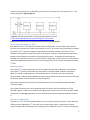
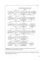
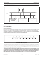
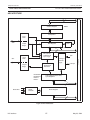
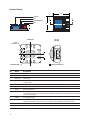
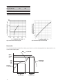
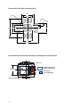
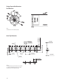
1
CORNELL UNIVERSITY Using I2C on an NXP Microcontroller Ruina Biomechanics Lab Michael Digman – Senior – ECE – MAE 4900 – 3 Credits 4/29/2011 Author Contact Information Address: 232 E. Irvin Ave., Hagerstown MD 21742 Phone: 814-634-4626 Email: [email protected] Abstract This report walks through the implementation of the protocol on a microcontroller with the purpose of establishing communication with a color sensor. The basics of communication are presented. Details of necessary to the communication with the color sensor are provided in full. This report provides register-level detail on the steps necessary to drive an NXP controller as a master in order to communicate with a color sensor acting as a slave on an bus. Processing results from the color sensor is additionally discussed. Table of Contents Abstract .................................................................................................................................................. 1 Table of Contents .................................................................................................................................... 1 Introduction ............................................................................................................................................ 3 Motivation of Report ........................................................................................................................... 3 Hardware Used and Implied Limitations .............................................................................................. 3 Physical Design and Intent of Color Sensor Use .................................................................................... 3 Background ............................................................................................................................................. 4 I2C Communication Protocol ................................................................................................................ 4 General Description ......................................................................................................................... 4 Physical Description ......................................................................................................................... 4 Device Operation: Master or Slave ................................................................................................... 5 Operating Modes ............................................................................................................................. 5 Slave Device Addressing................................................................................................................... 5 Physical Layer Protocol Description.................................................................................................. 6 Software Layer Protocol Description: Writing Data to Slave ............................................................. 7 Software Layer Protocol Description: Reading Data from a Slave ..................................................... 8 I2C Debugging, Errors and Problem Resolution ................................................................................. 9 Color Sensor Gain Adjustment ............................................................................................................. 9 Capacitors........................................................................................................................................ 9 Integration Time .............................................................................................................................. 9 When is Gain Adjustment Necessary? ............................................................................................ 10 Methods and Results ............................................................................................................................. 10 1 Implementing I2C with the LPC2194 Microcontroller.......................................................................... 10 Basic Hardware Interface ............................................................................................................... 10 I2C Control Register Overview ........................................................................................................ 11 Setup of I2C Hardware.................................................................................................................... 12 Data Transfer Overview: Monitoring SI and Checking for Proper Status Codes ............................... 12 Abstracting the I2C Communication Protocol.................................................................................. 16 Effect of Noise on I2C Communication ............................................................................................ 16 Processing Results from the Avago Color Sensor ................................................................................ 16 Removing Influence of Gain: Effect of Capacitors and Integration Time.......................................... 16 Automatic Gain Adjustment ........................................................................................................... 18 Fastest Color Sensor Sampling Speed ............................................................................................. 19 Attenuating Influence of Fluorescent Light Flickering on Color Readings ........................................ 20 Overclocking the Color Sensor’s I2C Port ........................................................................................ 22 Effect of Light Source on Color Readings ........................................................................................ 22 Conclusions ........................................................................................................................................... 23 Appendix ............................................................................................................................................... 23 2 Introduction Motivation of Report The intent of this work is to enable the reader to implement the basic elements of the communication protocol on a microcontroller so that communication with a color sensor can be established. The protocol will be discussed with enough detail to understand the communication necessary to request and to receive readings from a slave color sensor. This report walks the reader though the integration of the ADJD-S371-QR99 Digital Color Sensor with an NXP LPC2194 microcontroller. Methods for processing the results received from the Avago color sensor are discussed. This enables the reader to understand the process involved in integrating, debugging and improving color sensor readings received over . Hardware Used and Implied Limitations The color sensor used for this project is the ADJD-S371-QR99 Digital Color Sensor Module from Avago Technologies. This color sensor features only one communication bus that uses the protocol at a max speed of 100 kbit/s. The sensor takes readings of red, green, blue and clear color values. The NXP LPC2194 microcontroller features a 32-bit ARM7TDMI-S processor and with an bus capable of communication at 400 kbit/s. To ensure no data loss and no corruption, 100kbit/s is the maximum speed at which the communication between the microcontroller and the color sensors should be conducted. The result of running the bus at a rate higher than 100 kbit/s is discussed in Methods and Results. Additionally, because the Avago color sensor has a static slave address, only one color sensor may be attached on the same bus. This means that it is not possible to connect more than one Avago color sensor to the same port on the LPC2194 microcontroller. Please note that the same peripheral is used in other NXP 2000 and 3000 series microcontrollers. The LPC2114, 2119, 2129, and 2194 all have identical bus hardware. This guide can function properly using any microcontroller with an identical bus controller. Physical Design and Intent of Color Sensor Use The Avago color sensor is housed in a custom casing that places the sensor behind a 2 inch Fresnel lens with a focal length of 1.5 inches. This can be seen in Figure 1. 3 Figure 1. The physical casing of the Avago color sensor. Background I2C Communication Protocol The only communication protocol used by the Avago color sensor is . This means that the LPC2194 microcontroller must use the capabilities of its hardware to receive data from the Avago color sensor. The scope of this section intends to educate the reader to the extent necessary to understanding the communication between the Avago color sensor and the microcontroller. The color sensor operates as a slave to the master microcontroller. As such, this section is written from the perspective of the master microcontroller. General Description is a multi-master, single-ended, serial communication protocol developed by Philips for embedded systems. As is shown later, is not—by default—a balanced differential communication protocol; any noise injected into a signal cannot be systematically removed at a later time. For use in this project, only two main tasks are completed though the use of . enables the microcontroller to receive sensor readings from the color sensor. also enables the microcontroller to set the value of configuration registers on the color sensor. Physical Description To operate an bus, two wires are required: SCL and SDA. SDA is the data line; its main purpose is to move data from across the bus. SCL is the clock line; its main purpose is to synchronize data transfers that occur on the bus. Every device using the bus is connected to SCL and SDA. Both SCL and SDA lines are considered to be open drain. This means that any device connected to an bus can drive the SCL and/or the SDA lines low, but they cannot drive either line high. The lines are driven high by two 4 resistors connected from Vcc to SDA and from Vcc to SCL. The value of Vcc in this project is +5 V. This setup is displayed in Figure 2Figure 2. . Figure 2. The basic setup of the communication protocol. Source: http://www.robot-electronics.co.uk/acatalog/I2C_Tutorial.html Device Operation: Master or Slave Each device on the bus operates in either master or slave mode. A master device drives the SCL clock line. Only a master can initiate a data transfer on the bus; slaves may only respond to requests by masters. The protocol supports multiple slaves and multiple masters on the same bus, however that complexity is beyond the scope of information necessary to understand communication between the LPC2194 microcontroller and the Avago color sensor. Throughout this document the LPC2194 microcontroller functions as a master while the Avago color sensor functions as a slave. Due to constraints established by the color sensor, only one Avago color sensor may be connected to the same bus. Operating Modes The master in may be operating in one of two modes that describes its behavior in the software layer of the protocol. The master may enter Master Transmitter Mode. In Master Transmitter Mode, the master is sending data to a receiving slave device. The master may also enter Master Receiver Mode. In Master Receiver Mode, the master pulses the SCL line but allows a slave to write onto the SDA; the master receives data from a transmitting slave. Slaves enter states with similar behaviors. Slave devices may enter Slave Receiver Mode and Slave Transmitter Mode. Error codes are based on the current operating mode of a device. NXP, the manufacturer of the LPC2194, supplies a table of error codes that is segmented into sections for each of the possible modes of operation. For debugging purposes, it is very important to know what operating mode the master is in. Slave Device Addressing All slaves on an bus must have two address: one to read from and one to write to. These addresses differ by one bit. Addresses in are used, in the context of this project, to alert slaves of a data transfer request and to notify slaves of an impending write. Addresses in the protocol are eight bits 5 wide. This implies that up to 64 slaves can be on a single bus. Address bits 1:7 can be considered the slave locator; these bits uniquely identify a device on the bus. Address bit 8 is an indicator of the desire to read or write. This address scheme can be seen in Figure 3. If bit 8 is set to zero it signifies a desire to write to the address in bits 1:7, if bit eight is set to one is signifies a desire to read from the address in bits 1:7. Figure 3. Slave addressing. A6:A0 refers to the device locator. R/W refers to the read or write bit. Source: http://www.sparkfun.com/datasheets/Sensors/Imaging/AV02-0314EN.pdf It is important to note that the Avago color sensor, described under Introduction, has a permanent device locator (address bits 1:7), in hex, of 0x74. This means that to write to the color sensor registers the address, in hex, of 0xE8 must be used. To read from the color sensor registers the address, in hex, of 0xE9 must be used. The other implication of a permanent device locator is that only one Avago color sensor may be placed on a bus. Every slave attached to an bus must have a unique address. The address of the color sensor cannot be modified so it is not possible to have two Avago color sensors on the same bus, because they both would have the same device locator. Physical Layer Protocol Description The master initializes and stops all data transfers. To signal the beginning of data transfer, in , the master must issue a START condition. This is defined as a high to low transition on SDA while the SCL is high. The master may terminate the current data transfer by issuing a STOP condition. This is defined as a low to high transition on SDA while SCL is high. The repeated START condition may also be sent; it is used when transferring modes (Master Receiver to Master Transmitter) without the need to send a STOP condition. The START and repeated START conditions are functionally identical, but the use of a repeated START condition prevents the unnecessary signaling of a STOP condition. Data is transferred in sequences of eight bits or one byte. The bits are placed on the SDA line (by either the master or the slave), with the most significant bit going first. During the data transfer the master holds the SCL line low, and releases the SCL—on clock cycles—to make it go high. This effectively creates a clock. The value of the SDA line, when SCL goes high, is the bit transferred. For every eight bits transferred an acknowledgement bit is send from recipient to sender. This means that nine SCL pulses are used for every eight bits of data sent. This acknowledgment bit is used to identify potential errors that may have occurred during transfer. 6 Figure 4. Example of the Transfer of Two Bytes of Data. The second data byte was followed by a NO ACK, meaning that an error occurred in transmission. Source: http://www.sparkfun.com/datasheets/Sensors/Imaging/AV02-0314EN.pdf Software Layer Protocol Description: Writing Data to Slave To provide configuration settings to the color sensor, it is necessary to have the ability to write to registers on the color sensor. Assuming that the color sensor has implemented properly, all the master has to do is tell the slave (at a certain address) what register it wishes to write to and what value the slave should put into that register. Note that due to the limitations of data transfer it is possible, but more complicated to write to registers that are larger than one byte in size. The protocol requires the master to complete the following steps in chronological order to write to a slave. This process is depicted in Figure 5. 1. The master issues a START condition. a. If the line is still busy (a start condition has been issued previously, but no stop condition has been issued yet) the master will issue a repeated START condition. 2. The master puts the slave address on SDA and waits for the ACK from the addressed slave. a. The address of the slave must contain zero in the eighth bit to signify the desire to write. 3. On receipt of ACK in step 2, the master puts the register address it wishes to write to, on the slave from the address in step 2, on the SDA. The master then waits for the ACK from the slave with the address from step 2. 4. On receipt of ACK, the master puts the value of the register it wishes to write into the slave’s register from step 3. The master then waits for the ACK from the slave with the address from step 2. 5. On receipt of the ACK, the master issues a STOP condition. 7 Figure 5. Diagram depicting the process followed for a master to write to a slave device. Source: http://www.sparkfun.com/datasheets/Sensors/Imaging/AV02-0314EN.pdf Figure 5 shows that it takes 8*3+4=28 bits to write to a register on a slave device. Software Layer Protocol Description: Reading Data from a Slave In order to retrieve data from the color sensor, it is necessary to have the ability to read from registers on the color sensor. Assuming that the color sensor designers have properly implemented , the master will need to notify the slave color sensor (at a certain address) which register it wishes to read from. In order to send the register address to the slave, the master must make the slave believe it will be written to. After writing to inform the slave what register the master wishes to read, the master must request to read from the slave. The slave then enters transmitter mode (although the master still controls the clock) and writes requested register’s value onto the SDA line. Note that if the slave’s requested register is larger than eight bits wide, a mapping will occur between the register address and bits within the register. In the case of the Avago color sensor, the color sensor measurement registers are 10 bits wide. Unique register addresses are assigned to bits 0:7 and bits 8:9. The protocol requires the master to complete the following steps in chronological order to read from a slave. This process is depicted in Figure 6. 1. The master issues a START condition. a. If the line is still busy (a start condition has been issued previously, but no stop condition has been issued yet) the master will issue a repeated START condition. 2. The master puts the slave address on SDA and waits for the ACK from the addressed slave. a. The address of the slave must contain zero in the eighth bit to signify the desire to write. Writing is necessary here as the master must send the address of the register that it desires to read. 3. On receipt of ACK, the master puts the register address it wishes to read from, on the slave from the address in step 2, on the SDA. It then waits for the ACK from the slave with the address from step 2. 4. On receipt of the ACK, the master issues a repeated START condition. 5. The master puts the slave address on SDA and waits for the ACK from the addressed slave. a. The address of the slave must be set to one in the eighth bit to signify the desire to read. 6. On receipt of the ACK, the master must pulse SCL eight times. This allows the slave to put the value of the requested register, from 2, on to SDA to be received by the master. Once the 8 master has received all necessary data it puts a NOT ACK onto SDA to tell the slave, that just transferred data, that all information has been properly received. 7. The master issues a STOP condition. Figure 6. Diagram depicting the process followed for a master to read from a slave device. Source: http://www.sparkfun.com/datasheets/Sensors/Imaging/AV02-0314EN.pdf Figure 6 shows that it takes 4*8+7=39 bits to complete the reading of one register from a slave device. I2C Debugging, Errors and Problem Resolution Sending and receiving data using the protocol is not flawless; errors may occur. However, after every byte is sent an ACK or NOT ACK is returned by the recipient. If a NOT ACK is returned when a master is sending data to a slave, the master knows to resend the previous byte. For this project, information on errors is made available through status registers associated with the hardware on the LPC2194 microcontroller. This ensures that if communication between master and slave is functioning, any noticeable problems will be reported. Color Sensor Gain Adjustment The color readings outputted by the color sensor are a function of eight parameters set by the user. In this work it is assumed that the values read from the color sensor obey the following relationship: = ∙ Here, G is known as the gain of the color sensor. The gain is a function of the eight parameters mentioned above. Capacitors The first four parameters are the number of capacitors used to detect each color; the red, blue, green and clear sensors can use a minimum of 0 and maximum of 15 capacitors each. Using 0 capacitors, for any color, effectively sets any reading of that color to zero. For values greater than 0, the color sensor application note states “a higher capacitance value will result in lower sensor output.”1 Integration Time The last four parameters of gain adjustment deal with the integration time of each color: red, green, blue and clear. These parameters describe the length over which sensor data will be summed for each 1 http://www.sparkfun.com/datasheets/Sensors/Imaging/AV02-0359EN.pdf, page 2 9 color. Integration time values are limited to the decimal range of 0 to 4095. However, data sheets provided by the manufacturer do not state the relationship between time and the value set for integration time; it is guessed that the integration time setting refers to the number of clock cycles that occur within the color sensor. When is Gain Adjustment Necessary? The maximum reading possible for any color sensor output is limited by the 10 bits of resolution used to store each color’s reading. This implies that value of the sensor reading for each color can range from 0 to 1023. If the current gain settings produce sensor readings of the value 1023, it is likely that the color sensor is being oversaturated because the current gain setting it too high. If the current gain settings produce sensor readings of the value 0, or close to it, gain is likely set too low. In either of these cases it is necessary to change the gain in order to get accuracy from sensor readings. Methods and Results Implementing I2C with the LPC2194 Microcontroller Basic Hardware Interface The NXP interface is controlled by setting and reading values of registers reserved for the module. On the LPC2194 NXP microcontroller, seven registers are reserved to control the hardware interface. Page 177 of the user manual for the LPC2194 microcontroller contains the names, basic functionality, reset values and address of these registers. Throughout the rest of this section, registers will be referred to by the names listed by the user manual. For reference, the table is listed in Figure 7. Figure 7. Names, basic functionality, reset value and addresses of registers assigned for the hardware on the LCP 2194. Source: http://www.keil.com/dd/docs/datashts/philips/user_manual_lpc2119_2129_2194_2292_2294. pdf I2CONSET is used to actively control most functionality of the hardware. I2STAT contains the a status code associated with an the most recent interrupt issued (from the SI bit in I2CONSET). I2DAT is written to when information is to be sent to a slave device, I2DAT also contains data received from slave devices. I2SCLH and I2SCLL are registers used to control the speed at which the interface operates. 10 I2CONCLR is the clear register for I2CONSET. The registers I2ADR is of no use to this project as the LPC2194 will never be operating as a slave. Interfacing with a Set Register I2CONSET’s access is described as “read/set.” Set access means that when writing to the register only values of one will be written, values of zero will not alter the register’s value. For example if a set access register’s current value, in binary, 0b10101010 and the value, in binary, 0b01010101 is written to it the stored value will be, in binary, 0b11111111. Interfacing with a Clear Register I2CONCLR’s access is described as “clear only.” I2CONCLR is the only way to set bits of the I2CONSET register to zero. Writing a 1 to any bit of I2CONCLR will clear the corresponding bit in I2CONSET. For example, writing 1 to bit 5 of I2CONCLR will set bit 5 of I2CONSET to 0. Clear registers do not store any information, and can be thought of as a means to issue a command. This means that to clear bits 4 and 6 (numbering begins at 0) of I2CONSET the value, in binary of 0b01010000 can be written to I2CONCLR. However, because I2CONCLR does not store values, the same effect can be achieved by writing, in binary, 0b01000000 to I2CONCLR followed by writing, in binary, 0b00010000 to I2CONCLR. I2C Control Register Overview Each bit used to control the module on the LPC2194 has a name that describes its functions. These names can be found on page 169 of the LPC2194 user manual. For reference, these names and the corresponding bits are listed in Figure 8. Bits 7, 1 and 0 of I2CONSET are reserved bits and should not be written to or read from as the resulting behavior is undocumented. Figure 8. Names and corresponding bits of the control register, I2CONSET. Source: http://www.keil.com/dd/docs/datashts/philips/user_manual_lpc2119_2129_2194_2292_2294. pdf Bit 6: I2EN When I2EN is high the work properly. hardware is enabled. I2EN must be set to 1 for any of the functions of to Bit 5: STA STA corresponds to the START condition. When STA is high the hardware generates a START condition or a repeated START condition, which are functionally identical. It is necessary to clear STA after receiving a status code that indicates that the START or repeated START condition has been sent on SDA. STA is cleared by writing 1 to bit 5 of I2CONCLR. 11 Bit 4: STO STO corresponds to the STOP condition. When STO is 1, a STOP condition is transmitted on the I2C bus. When the bus detects the STOP condition, STO is cleared automatically; there is no need to clear the STO bit. Bit 3: SI SI corresponds to an interrupt flag. This bit is set high by the hardware when one of several events is detected. When SI is high the value of register I2STAT is set to a status code. This bit must be monitored to enable data transfer. Page 24 of the NXP user manual on their interface contains the full list of status codes that correspond to events detected by the hardware. To see more information on status codes and how they are used in the flow of data transfer see the Data Transfer Overview section. SI is cleared to continue operation of the hardware. SI should be cleared after it is set high by the hardware and the status code in I2STAT is noted. SI is set to zero by writing a 1 to bit 3 of the I2CONCLR register. Bit 2: AA AA corresponds to the Assert Acknowledgment flag. For this project, the microcontroller will only be operating as a master. If only operating as a master, AA must always be set to 0. However, because I2CONSET is a set register, setting AA to 0 is only possible by writing a 1 to bit 2 of the I2CONCLR register. Setup of I2C Hardware For any of the functionality of the high. hardware to be operational bit 6, I2EN, of I2CONSET must be set In addition, the rate at which the hardware operates needs to be set by writing to the I2SCLH and I2SCLL registers. The Avago color sensor is limited to a transmission speed of 100 kHz, so for this project the interface on the LPC2194 microcontroller is set to 100 kHz. Details on setting the microcontroller for other speeds can be found on page 175 of the LPC2194 user manual. For the use of this project the microcontroller was set to use no VPB Clock Dividers. Data Transfer Overview: Monitoring SI and Checking for Proper Status Codes The flow of a data transfer operation hinges on the value of the SI bit in the register I2CONSET. SI is set high by the hardware when one of several events is detected. After every step in the data transfer process, the microcontroller must monitor SI to see if the operation was completed successfully (by checking the status code in I2STAT) and only then may the microcontroller continue transferring data. Status codes are issued by hardware after the interrupt bit, SI, is set high. Status codes differ for the mode in which the master is operating; see Operating Modes in the Communication Protocol for more information. The statuses of interest to this project are: Successful sending of a START condition Successful sending of a repeated START condition 12 Slave address transmitted and ACK received Slave address transmitted and NOT ACK received Data byte transmitted and ACK received Data byte transmitted and NOT ACK received Data byte received and ACK returned Data byte received and NOT ACK returned Note that there is no status code associated with the successful sending of a STOP condition. After sending a STOP condition the SI bit will not be set high. Writing Data to a Slave Device As an example of how SI and status codes are used, Figure 9 shows the steps the microcontroller should perform in order to write data to a slave over . See the Background section on the Software Layer Protocol Description for writing data to a slave to understand the general procedure. Figure 9. Flow chart detailing what the microcontroller must do in order to control the hardware interface to write data to a slave device. 13 Note that, as mentioned in the section on Bit 5: STA, the STA must be set to 0 after successfully sending a START condition. As long as the STA bit is high the interface will attempt to send START or repeated START conditions. Reading Data from a Slave Device Figure 10 shows the steps the microcontroller should perform to read from a slave device over . 14 Figure 10. Flow chart detailing what the microcontroller must do in order to control the hardware interface to read data from a slave device. See the Background section on the Software Layer Protocol Description for reading data from a slave to understand the general procedure. 15 Abstracting the I2C Communication Protocol To make interfacing with the protocol simple, it is necessary to abstract the physical layer commands to high-level. Proper abstraction will allow a single line for the master to request and recover data from the Avago color sensor. The transfer of data in always begins with a START condition and ends with either a repeated START (to signal a change of the master's mode) or a STOP condition. As the intent of a user may not be known, when abstracting the protocol it is simplest to give the user direct control sending START, repeated START and STOP signals. Additionally, hardware requires that data be present on the SDA line before the master microcontroller will begin sending data. It is possible to abstract this up to the function level so that the user is capable of sending (loading SDA, then setting proper control bits of microcontroller) data. These functions can be joined together to perform the operation of reading and writing to a slave, as described in the Background section under Software Layer Protocol. Finally, these operations can be joined together to form several read and write operations that allow for a single function to read all values of the color sensor or write all settings to the color sensor. Effect of Noise on I2C Communication Noise injected on a standard bus is not removed by differential amplification. The standard bus is not balanced, so noise spikes look like signal to devices attached to the bus. This noise can induce random effects during transmission. It is important to note that there is no timeout in communication. Once a START condition has been sent, the bus is considered busy until an END condition is sent. For this reason, if noise is a concern, it is good practice to start a timer when waiting for the event interrupt, for the SI bit to go high. If the timer counts past a predefined timeout value this likely means that the master and/or slave device is waiting for an event to happen that has already occurred, but could not be detected (or was falsely detected) because of noise. At this point, resetting the hardware interface is a potential solution. Noise was an issue for the Avago color sensor interface in this project. The LPC2194 microcontroller and bus is mounted close to a motor that could potentially draw high currents over short periods of time. These currents produced large electric and magnetic fields physically close to the interface of the LPC2194 microcontroller, and evidently led to electromagnetic interference on the bus. This noise was frequently found to stop communication between the microcontroller and the Avago color sensor. Implementing a timeout, while waiting for the SI bit to go high, solved the problem. Processing Results from the Avago Color Sensor Removing Influence of Gain: Effect of Capacitors and Integration Time In some fashion, gain is a function of both the number of capacitors enabled and the integration time over which a color sensor sums readings. For more information on the operation of the Avago color sensor see the Background section on Color Sensor Gain Adjustment. Multiple experiments were conducted to compare the influence of capacitors and integration time on gain. 16 The first experiment required the setup of a white LED pointed directly at the Avago color sensor in a dark room. The number of capacitors for all colors was set at 1 while the integration time was swept from about 125 until a color sensor reached a maximum output of 1023. The results are displayed in Figure 11. Figure 11. Each color displayed a highly linear relationship when the number of capacitors was constant and the integration time of each color was swept from 125 until the maximum reading was encountered. Figure 11 shows a highly linear relationship between integration time and each sensor’s output. Note that the LSQR of every color of the color sensor produced a model with a non-zero y-intercept. Multiple experiments showed that this y-intercept varied in ways unpredictable to the author for every color of the color sensor. However, the magnitude of this y-intercept is, on average, approximately 7. Because the magnitude of the y-intercept is small compared to sensor values (that normally range from 50 to 900), the y-intercept of every LSQR model was forced to zero. Setting the y-intercept to 0, the smallest value encountered was 0.9993 using LSQR. The second experiment also required the setup of a white LED pointed directly at the Avago color sensor in a dark room. In this case the gain was kept constant and the number of capacitors was changed. No observable influence was detected, as the sensor’s output values were approximately constant. While more throughout testing would be required to determine the exact relationship of the number of capacitors and the integration time had on gain, this information was enough to construct a simple model that would allow for comparison of values of different gains. These experiments showed that any influence that the number of capacitors had on the gain was minimal. It was therefore assumed that the gain was a function of only integration time. 17 ∝ This means that the integration time is directly proportional to the sensor output, any other proportional constants are assumed to be constant among all sensors and is embodied in the variable . This can be expressed as: = ( )∙ To compare sensor outputs, assuming is constant for all colors in the color sensor, all that is necessary is to divide the sensor output by integration time. This, assuming all the assumptions made before are correct, means that it is possible to remove the effect of gain on sensor readings. The validity of this statement can be tested by taking the results from the first experiment, shown in Figure 11, and dividing the sensor output by the integration time. The result should be a constant value because the input light source does not change. This is shown in Figure 12. The are approximately constant for all integration times. Variations in the curve likely come from assuming that the y-intercept of the lines in Figure 11 was 0 and that the number of capacitors used had no effect on the gain of the system. Figure 12. The gain of the color sensor can be approximately removed by dividing the color sensor value by its corresponding integration time. Automatic Gain Adjustment The Avago color sensor in this project was intended to be attached to a moving robot, potentially travelling through areas of bright or dim lighting. To accommodate for constant changes in the intensity of light seen by the color sensor an automatic gain adjustment algorithm was implemented. Because the 18 effect of the gain is removed by division of the integration time (see Removing Influence of Gain on Sensor Readings), it is possible to compare sensor readings for any gain setting. This means that the integration time can be switched at will with no apparent effect on the sensor readings, making automatic gain adjustment possible. A simple gain adjustment algorithm was implemented. Gain adjustment is necessary when any sensor reading becomes close to 1 (increase gain) or close to the max value of 1023 (decrease gain). The following algorithm was used: If any sensor reading < 100 ) ≤ 4095, multiply the current integration time of all colors by o If 2 ∙ ( 2. This was implemented by checking to see if the integration time was ≤ 2047 If it was, then = ≪2 o Otherwise, the minimum resolution of the sensor has been reached. It is not possible to get a better reading. If any sensor reading is > 900 o o If ≥ 2, divide the current integration time of all colors by 2 This was implemented by checking to see if the integration time was ≥ 2 If it was, then = ≫2 Otherwise, the maximum resolution of the sensor has been reached. It is not possible to get a better reading. This algorithm is initialized by assigning the same integration time value to all sensors. The initial integration time value is such that it normally produces color sensor values within the range 0 to 1023 under standard room lightning conditions. This gain adjustment algorithm was run every time any of the sensor’s outputted readings were less than 100 or greater than 900. Note that it is possible to run separate gain adjustments on each of the individual color channels. For the sake of simplicity, gain adjustments are applied uniformly to each color of the color sensor. Fastest Color Sensor Sampling Speed At the best, assuming no errors in transmission, it takes 28 bits to write to a register on a slave and 39 bits to read from a register on a slave (see the Background section on Communication Protocol). To request and receive sensor readings from the Avago color sensor the following operations need to be completed: 1. 2. 3. 4. 5. 6. 7. Write to the Avago color sensor control register to request reading Read from the Avago color sensor control register to see if sensor values are ready Read from the red low register (readings are 10 bits wide) Read from the red high register Read from the blue low register Read from the blue high register Read from the green low register 19 8. Read from the green high register 9. Read from the white low register 10. Read from the white high register This totals 1 write operation and 9 read operations or 1*28+39*9=379 bits to take readings from all colors on the color sensor. The Avago color sensor can, at maximum, operate its bus at 100kbit/s. At the absolute best, assuming no lag between any of read or write operations and 0 seconds required for the color sensor to generate readings, the fastest the device could operate is ∗ = 3.79 ms to request and receive one reading: this which is equivalent to about 264 Hz. Please note that reading from the low or high red, blue, green and white color sensor value registers while the Avago color sensor is currently taking measurements is unsupported. Reading should not be done in parallel with waiting for the interrupt. Attenuating Influence of Fluorescent Light Flickering on Color Readings In the United States, due to the frequency of AC power provided, fluorescent lights ramp from zero light to full intensity and back down to zero at a rate of about 120 Hz. Using the Avago color sensor, amplitude flickering can be detected in every color of the color sensor at about 120Hz when the color sensor is placed under fluorescent lighting conditions. Efforts were made to sample the light at an interval that would severely retard the amplitude of the swing induced by the flickering of the fluorescent lights. If perfect timing was possible, aliasing of the signal could be completed such that the sensor readings appeared as if no sinusoid was present. Sampling at = = ∗ Hz, where N is a positive non-zero integer, will produce an output aliased so that the effect of the light swing will be removed. Setting = 1, = 240 retains the maximum number of samples. This is shown in Figure 13. Even when noise is injected in the sample times (at a fraction of ) very little disturbance in amplitude is seen. 20 Figure 13. Sampling a sinusoid at = 2 = 2 ∗ 120 an aliased result that appears constant. produces However, as shown in the Minimum Speed of Operation section, this speed is close to the theoretical maximum so it is unlikely possible to operate the Avago color sensor at this speed. Setting = 13, = 18.462 was applicable in our project after all delays were accounted for. Note that this low speed was used to accommodate for integration time necessary for low light settings. Using internal clocks on the LPC2194 it was possible to achieve a sampling rate of approximately 18.5 Hz. Assuming = 18.5 , the aliased data appears sinusoidal with an envelope. Every sample swings across the DC component of the sinusoid. For example, sample 10 is above the DC component while sample 11 is below the DC component. Using an averager on data with rapid swings allows for the DC component to be converged upon quickly. Implementing an exponential averager on the sampled data reduced the amplitude of the sinusoid to approximately 3% of its original value. This can be seen in Figure 14. 21 Figure 14. Sampling a sinusoid at = 18.5 produces a sinusoid a high frequency sinusoid with an envelope that is 2 seconds long. Using an exponential averager (pictured is of length 16) it is possible to reduce the amplitude of the fluorescent sinusoid to about 3% of the original amplitude. Overclocking the Color Sensor’s I2C Port The Avago color sensor’s spec sheet lists its maximum transmission speed at 100kbit/s. Several attempts were made to run the Avago color sensor at speeds greater than 100kbit/s. In all circumstances, randomly timed spikes would appear in sensor output. The amplitude of these spikes was the maximum value attainable from any color sensor reading: 1023. Consistent data from the color sensor was needed over time, so the speed of the had to be reduced to 100kbit/s. In applications where random data spikes may not be influential, it is possible to overclock the Avago color sensor’s port. Effect of Light Source on Color Readings Light incident on a surface changes its apparent color. The value of colors sensed on a surface illuminated with an overhead fluorescent light is different than the value of colors sensed on the same surface that is exposed to natural light. Incident light has some color component. Using color sensors in an area that has a light source which is changing over time (like fluorescent to natural) will bring about complications. The red, green and blue components that specify a green floor segment at time may be different than at time . This makes ratios of colors unstable over time. 22 Experimentation under all possible light sources is necessary to understand how colors will change over time. The initial purpose of integrating this color sensor with an NXP LPC2194 was to aid in the driving of a robot autonomously on an indoor track over extremely long lengths of time. This track was Barton hall at Cornell University. The hall is illuminated during day time with natural light; at night fluorescent light fills the room. Due to the fact that color sensor readings changed with time, it became very difficult to determine a method of uniquely identifying a color at any one time because of the unstable color readings. Conclusions Implementing to interface between one master and a slave device is possible using the contents of this report. This report shows the efficacy of using an NXP LPC2194 microcontroller to interface with the ADJD-S371-QR99 Digital Color Sensor from Avago. Readings from the Avago color sensor can be processed to remove the influence of gain therefore making sensor values comparable. By sampling correctly it is possible to attenuate the effect of fluorescent light flickering on color sensor readings. If monitoring content where the light intensity fluctuates, it is possible to have the color sensor adjusted automatically so that no readings are over saturated or under saturated. The hope of this report is also to educate readers on what cannot be done with the Avago color sensor and LPC2194 interface. It is theoretically impossible to receive every color reading from the color sensor at a rate faster than about 264 Hz. Overclocking the Avago color sensor bus produces spikes in readings. Environmental noise cannot always be ignored; it may require the use a timeout to ensure that operation continues successfully. The protocol has more capability than what is represented in this document. For example, has a protocol to deal with multiple masters. The LPC2194 may also act as a slave on an bus. Similarly, the Avago color sensor contains more features than those detailed in this document. For example, the color sensor allows for a user supplied offset to be subtracted from all readings. The Avago color sensor also has a low power mode in which it may operate. Despite these short comings, it is the belief of the author that this document contains all information essential to enable the LPC2194 microcontroller to request and receive data from the ADJD-S371-QR99 Digital Color Sensor from Avago. Appendix Content in the appendix is placed in this order: 1. 2. 3. 4. Code used in project to abstract I2C interface Portion of the NXP LPC2194 user manual on the interface Status codes assigned to I2STAT on the NXP LPC2194 Avago ADJD-S371-QR99 Digital Color Sensor Datasheet 23 5. Avago ADJD-S371-QR99 Register List 24 C:\Users\Template\Desktop\Final Report\i2c_color.c Tuesday, May 03, 2011 12:44 PM /** @file i2c_color.c Contains i2c communication procedure Runs gain optimization Returns r,g and b values from color sensor @author Michael Digman @date December 2010 */ #include <includes.h> //define global variables unsigned long int i2c_clear_data; unsigned long int i2c_red_data; unsigned long int i2c_blue_data; unsigned long int i2c_green_data; unsigned long int i2c_clear_data_avg; unsigned long int i2c_red_data_avg; unsigned long int i2c_blue_data_avg; unsigned long int i2c_green_data_avg; short int state_color_update; short int step; short int state_send_data; short int state_request_receive_colors; unsigned long timestampo = 0; unsigned short int integration_time = INT_ALL_VAL; void i2c_color_update(void){ unsigned char debug = 0; switch(state_color_update){ case 0: //1) check for color sensor /*debug = find_sensor(); //if(debug == 0xFF){ //sensor is found //state_color_update = 1; //move to next state //step = 0; //reset current step }*/ state_color_update = 1; break; case 1: //2) perform gain optimization debug = gain_optimization(integration_time); if(debug == 0xf0){ //gain complete state_color_update = 2; step = 0; state_request_receive_colors = 0; } break; case 2: //3) return currently visible colors debug = request_receive_colors(); if( debug == 0xfe ){ //color request cycle complete, restart! state_request_receive_colors = 0; -1- C:\Users\Template\Desktop\Final Report\i2c_color.c Tuesday, May 03, 2011 12:44 PM //1) are any of the visible colors over the maximum value or below minimum? if( i2c_clear_data >= MAX_OK_VALUE || i2c_red_data >= MAX_OK_VALUE || i2c_blue_data >= MAX_OK_VALUE || i2c_green_data >= MAX_OK_VALUE ){ //readjust gain optimization if(integration_time >= MIN_INT_TIME){ integration_time = integration_time>>1; //divide by 2 state_color_update = 4; } else { //the integration time cannot be fixed, just collect data avg_colors(); } } else if ( i2c_clear_data <= MIN_OK_VALUE || i2c_red_data <= MIN_OK_VALUE || i2c_blue_data <= MIN_OK_VALUE || i2c_green_data <= MIN_OK_VALUE ) { if(integration_time <= MAX_INT_TIME){ integration_time = integration_time<<1; //mult by 2 state_color_update = 4; } else { //the integration time cannot be fixed, just collect data avg_colors(); } }else { //if the colors readings are great, average them! avg_colors(); } } break; case 3: //4) wait until timer says to resample if( T0TC < timestampo ){ state_color_update = 2; } break; case 4: //5) CALL GAIN OPTIMIZATION debug = gain_optimization(integration_time); if(debug == 0xf0){ //gain complete state_color_update = 2; step = 0; state_request_receive_colors = 0; } break; } } void avg_colors(void){ //remove dependance on integration time i2c_clear_data = get_absolute_reading(i2c_clear_data); i2c_red_data = get_absolute_reading(i2c_red_data); i2c_blue_data = get_absolute_reading(i2c_blue_data); i2c_green_data = get_absolute_reading(i2c_green_data); //average i2c_clear_data_avg = i2c_clear_data_avg - (i2c_clear_data_avg>>SHIFT) + (i2c_clear_data); -2- C:\Users\Template\Desktop\Final Report\i2c_color.c Tuesday, May 03, 2011 12:44 PM i2c_red_data_avg = i2c_red_data_avg - (i2c_red_data_avg>>SHIFT) + (i2c_red_data); i2c_blue_data_avg = i2c_blue_data_avg - (i2c_blue_data_avg>>SHIFT) + (i2c_blue_data); i2c_green_data_avg = i2c_green_data_avg - (i2c_green_data_avg>>SHIFT) + (i2c_green_data); timestampo = T0TC; //debug overrides //i2c_clear_data_avg = integration_time<<SHIFT; //get more colors! state_color_update = 3; } unsigned long int get_absolute_reading(unsigned long int reading){ return (reading<<12)/integration_time; } unsigned char i2c_check_output(unsigned char expected_status){ unsigned char debug = (((unsigned char)I2CONSET)&0x8)>>3; if(debug == 1 && I2STAT == expected_status) { debug = 0xff; } else { debug = I2STAT; }// we have a problem! return debug; } void i2c_send_START(void){ I2CONSET = 0x20; } //set STA bit high to signify START signal void i2c_send_STOP(void) { I2CONSET = 0x10; } void i2c_clear_SI(void) { I2CONCLR = 0x08; } //set SIC high void i2c_clear_STA(void) { I2CONCLR = 0x20; } //set STAC high void i2c_hardware_reset(void) { I2CONCLR = 0x6C; // sets AA to 0, SI to 0 STA to 0, I2EN to 0 I2CONSET = 0x40; //sets i2onset to -10000-} unsigned char find_sensor(void){ unsigned char debug = 0; switch (step) { case 0: i2c_send_START(); //send a start message step = 1; //move to the next state break; case 1: //wait for start SI debug = i2c_check_output(I2C_START_TRANSMITTED); if(debug == 0xff){//if start command is successfully transmitted //place slave address on line. I2DAT = SLAVE_WRITE_ADDR; //clear SI i2c_clear_SI(); //move to the next state step = 2; -3- C:\Users\Template\Desktop\Final Report\i2c_color.c Tuesday, May 03, 2011 12:44 PM } break; case 2: //wait ACK to be returned on slave address transmission debug = i2c_check_output(I2C_SLA_AND_W_ACKED); if(debug == 0xff){ i2c_send_STOP(); debug = 0xFF; //flag that it worked } break; } return debug; } unsigned char i2c_get_data(unsigned char addr){ static unsigned int counter = 0; unsigned char debug = 0; switch (state_send_data) { case 0: //send a start message i2c_hardware_reset(); //reset i2c_send_START(); state_send_data = state_send_data+1; //move to the next state counter = 0; break; case 1: //wait for start SI debug = i2c_check_output(I2C_START_TRANSMITTED); if(debug == 0xff){//if start command is successfully transmitted I2DAT = SLAVE_WRITE_ADDR; i2c_clear_SI(); i2c_clear_STA(); state_send_data = state_send_data+1; counter = 0; }else if(counter > MAX_CALLS){//interference problem, restart transmission from 0 i2c_send_STOP(); state_send_data = 0; }else{counter=counter+1;} break; case 2: //ensure that slave address has been acked debug = i2c_check_output(I2C_SLA_AND_W_ACKED); if(debug == 0xff){ I2DAT = addr; i2c_clear_SI(); state_send_data = state_send_data+1; counter = 0; }else if(counter > MAX_CALLS){//interference problem, restart transmission from 0 i2c_send_STOP(); state_send_data = 0; }else{counter=counter+1;} break; case 3: debug = i2c_check_output(I2C_DATA_ACKED); if(debug == 0xff){ //address has been sent properly! //ENTER MASTER RX MODE //RESEND START i2c_send_START(); -4- C:\Users\Template\Desktop\Final Report\i2c_color.c Tuesday, May 03, 2011 12:44 PM i2c_clear_SI(); state_send_data = state_send_data+1; counter = 0; }else if(counter > MAX_CALLS){//interference problem, restart transmission i2c_send_STOP(); state_send_data = 0; }else{counter=counter+1;} break; case 4: debug = i2c_check_output(I2C_REPEATED_START_TRANSMITTED); if(debug == 0xff){//if start command is successfully transmitted I2DAT = SLAVE_READ_ADDR; i2c_clear_STA(); i2c_clear_SI(); state_send_data = state_send_data+1; counter = 0; }else if(counter > MAX_CALLS){//interference problem, restart transmission i2c_send_STOP(); state_send_data = 0; }else{counter=counter+1;} case 5: debug = i2c_check_output(I2C_RX_SLA_AND_W_ACKED); if(debug == 0xff){ I2DAT = addr; i2c_clear_SI(); state_send_data = state_send_data+1; counter = 0; }else if(counter > MAX_CALLS){//interference problem, restart transmission i2c_send_STOP(); state_send_data = 0; }else{counter=counter+1;} break; case 6: debug = i2c_check_output(I2C_RX_DATA_REC_NOT_ACK_RET); if(debug == 0xff){ i2c_send_STOP(); i2c_clear_SI(); debug = 0xee; //inform caller to read from i2dat counter = 0; }else if(counter > MAX_CALLS){//interference problem, restart transmission i2c_send_STOP(); state_send_data = 0; }else{counter=counter+1;} break; } return debug; } unsigned char i2c_send_data(unsigned char data, unsigned char addr){ static unsigned int counter = 0; unsigned char debug = 0; switch (state_send_data) { case 0: //send a start message i2c_hardware_reset(); //reset -5- from 0 from 0 from 0 from 0 C:\Users\Template\Desktop\Final Report\i2c_color.c Tuesday, May 03, 2011 12:44 PM i2c_send_START(); state_send_data = state_send_data+1; //move to the next state counter = 0; break; case 1: //wait for start SI debug = i2c_check_output(I2C_START_TRANSMITTED); if(debug == 0xff){//if start command is successfully transmitted I2DAT = SLAVE_WRITE_ADDR; i2c_clear_SI(); i2c_clear_STA(); state_send_data = state_send_data+1; counter = 0; }else if(counter > MAX_CALLS){//interference problem, restart transmission i2c_send_STOP(); state_send_data = 0; }else{counter=counter+1;} break; case 2: //ensure that slave address has been acked debug = i2c_check_output(I2C_SLA_AND_W_ACKED); if(debug == 0xff){ I2DAT = addr; i2c_clear_SI(); state_send_data = state_send_data+1; counter = 0; }else if(counter > MAX_CALLS){//interference problem, restart transmission i2c_send_STOP(); state_send_data = 0; }else{counter=counter+1;} break; case 3: debug = i2c_check_output(I2C_DATA_ACKED); if(debug == 0xff){ //address has been sent properly! I2DAT = data; i2c_clear_SI(); state_send_data = state_send_data+1; counter = 0; }else if(counter > MAX_CALLS){//interference problem, restart transmission i2c_send_STOP(); state_send_data = 0; }else{counter=counter+1;} break; case 4: debug = i2c_check_output(I2C_DATA_ACKED); if(debug == 0xff){ //data has been sent properly! i2c_send_STOP(); debug = 0xee; counter = 0; }else if(counter > MAX_CALLS){//interference problem, restart transmission i2c_send_STOP(); state_send_data = 0; }else{counter=counter+1;} break; } return debug; -6- from 0 from 0 from 0 from 0 C:\Users\Template\Desktop\Final Report\i2c_color.c Tuesday, May 03, 2011 12:44 PM } unsigned char gain_optimization(unsigned short int integration_time_value){ //**** STEP 1 **** //Write sensor gain registers, CAP_RED, CAP_GREEN, //CAP_BLUE and CAP_CLEAR to select the number of //capacitor. The values must range from 00H to 0FH. A //higher capacitance value will result in lower sensor //output unsigned char debug = 0; switch (step) { case 0: debug = i2c_send_data(CAP_RED_VAL, CAP_RED); if(debug==0xee){ state_send_data = 0; step = step + 1; } break; case 1: debug = i2c_send_data(CAP_BLUE_VAL, CAP_BLUE); if(debug==0xee){ state_send_data = 0; step = step + 1; } break; case 2: debug = i2c_send_data(CAP_GREEN_VAL, CAP_GREEN); if(debug==0xee){ state_send_data = 0; step = step + 1; } break; case 3: debug = i2c_send_data(CAP_CLEAR_VAL, CAP_CLEAR); if(debug==0xee){ state_send_data = 0; step = step + 1; } break; /* STEP 2: Write sensor gain registers, INT_RED, INT_GREEN, INT_ BLUE and INT_CLEAR to select the integration time. The integration time registers is a 12-bit registers, the values is range from 0 to 4095. A higher value in integration time will generally result in higher sensor digital value if the capacitance gain registers have the same value(*/ case 4: debug = i2c_send_data(integration_time_value&0xff, INT_RED_LO); if(debug==0xee){ state_send_data = 0; step = step + 1; } -7- C:\Users\Template\Desktop\Final Report\i2c_color.c Tuesday, May 03, 2011 12:44 PM break; case 5: debug = i2c_send_data((integration_time_value&0xf00)>>8, INT_RED_HI); if(debug==0xee){ state_send_data = 0; step = step + 1; } break; case 6: debug = i2c_send_data(integration_time_value&0xff, INT_BLUE_LO); if(debug==0xee){ state_send_data = 0; step = step + 1; } break; case 7: debug = i2c_send_data((integration_time_value&0xf00)>>8, INT_BLUE_HI); if(debug==0xee){ state_send_data = 0; step = step + 1; } break; case 8: debug = i2c_send_data(integration_time_value&0xff, INT_GREEN_LO); if(debug==0xee){ state_send_data = 0; step = step + 1; } break; case 9: debug = i2c_send_data((integration_time_value&0xf00)>>8, INT_GREEN_HI); if(debug==0xee){ state_send_data = 0; step = step + 1; } break; case 10: debug = i2c_send_data(integration_time_value&0xff, INT_CLEAR_LO); if(debug==0xee){ state_send_data = 0; step = step + 1; } break; case 11: debug = i2c_send_data((integration_time_value&0xf00)>>8, INT_CLEAR_HI); if(debug==0xee){ state_send_data = 0; step = step + 1; } break; /* STEP 3: Acquire sensor digital values by writing 01H to CTRL register (address 00H). Then read CTRL register. When the value is 00H, the sensor digital values are read -8- C:\Users\Template\Desktop\Final Report\i2c_color.c Tuesday, May 03, 2011 12:44 PM from the sample data registers (address 40H to 47H). If these sensor digital values are not optimum, do another iteration loop consisting of step 2, 3 and 4*/ case 12: debug = request_receive_colors(); if( debug == 0xfe) { //all colors received //initalize average i2c_red_data_avg = get_absolute_reading(i2c_red_data)<<SHIFT; //i2c_red_data_avg =0; i2c_blue_data_avg = get_absolute_reading(i2c_blue_data)<<SHIFT; //i2c_blue_data_avg =0; i2c_clear_data_avg = get_absolute_reading(i2c_clear_data)<<SHIFT; //i2c_clear_data_avg =0; i2c_green_data_avg = get_absolute_reading(i2c_green_data)<<SHIFT; //i2c_green_data_avg =0; state_send_data = 0; state_request_receive_colors = 0; //send end code debug = 0xf0; } break; } return debug; } unsigned char request_receive_colors(void) { unsigned char debug = 0; switch(state_request_receive_colors){ case 0: //set control to 0x1 debug = i2c_send_data(0x01, CTRL); if(debug==0xee){ state_send_data = 0; state_request_receive_colors = state_request_receive_colors +1; } break; case 1: //read from control, is it 00? debug = i2c_get_data(CTRL); if(debug == 0xee) { //is control reading 00? if(I2DAT == 0){ //yes! read the colors state_send_data = 0; state_request_receive_colors = state_request_receive_colors +1; } else { state_send_data = 0; } } break; case 2: //read from red low debug = i2c_get_data( DATA_RED_LO); if(debug == 0xee) { i2c_red_data = I2DAT; state_send_data = 0; -9- C:\Users\Template\Desktop\Final Report\i2c_color.c Tuesday, May 03, 2011 12:44 PM state_request_receive_colors = state_request_receive_colors +1; } break; case 3: //read from red high debug = i2c_get_data( DATA_RED_HI); if(debug == 0xee) { i2c_red_data = ((I2DAT&0x3)<<8)|i2c_red_data; //merge colors state_send_data = 0; state_request_receive_colors = state_request_receive_colors +1; } break; case 4: //read from blue low debug = i2c_get_data( DATA_BLUE_LO); if(debug == 0xee) { i2c_blue_data = I2DAT; state_send_data = 0; state_request_receive_colors = state_request_receive_colors +1; } break; case 5: //read from blue high debug = i2c_get_data( DATA_BLUE_HI); if(debug == 0xee) { i2c_blue_data = ((I2DAT&0x3)<<8)|i2c_blue_data; //merge colors state_send_data = 0; state_request_receive_colors = state_request_receive_colors +1; } break; case 6: //read from green low debug = i2c_get_data( DATA_GREEN_LO); if(debug == 0xee) { i2c_green_data = I2DAT; state_send_data = 0; state_request_receive_colors = state_request_receive_colors +1; } break; case 7: //read from green high debug = i2c_get_data( DATA_GREEN_HI); if(debug == 0xee) { i2c_green_data = ((I2DAT&0x3)<<8)|i2c_green_data; //merge colors state_send_data = 0; state_request_receive_colors = state_request_receive_colors +1; } break; case 8: //read from clear low debug = i2c_get_data( DATA_CLEAR_LO); if(debug == 0xee) { i2c_clear_data = I2DAT; state_send_data = 0; state_request_receive_colors = state_request_receive_colors +1; } break; case 9: //read from clear high debug = i2c_get_data( DATA_CLEAR_HI); if(debug == 0xee) { -10- C:\Users\Template\Desktop\Final Report\i2c_color.c Tuesday, May 03, 2011 12:44 PM i2c_clear_data = ((I2DAT&0x3)<<8)|i2c_clear_data; //merge colors state_send_data = 0; debug = 0xfe; } break; } return debug; } //on implementation of public functions //use abstraction in data_nexus i2c_color section //as it is directly called by the can_setup function float i2c_get_white_data(void){ return (float) (i2c_clear_data_avg>>SHIFT); } float i2c_get_red_data(void){ return (float) (i2c_red_data_avg>>SHIFT); } float i2c_get_blue_data(void){ return (float) (i2c_blue_data_avg>>SHIFT); //return i2c_get_red_data()/i2c_get_green_data(); } float i2c_get_green_data(void){ return (float) (i2c_green_data_avg>>SHIFT); } void i2c_color_init(void){ //set internal state to 0 state_color_update = 0; step = 0; state_send_data = 0; state_request_receive_colors = 0; timestampo = 0; //PINSEL0 //PINSEL0 //PINSEL0 //PINSEL0 &=~(3<<4); &=~(3<<6); |=1<<4; |=1<<6; //set up appropriate data rate //I2SCLH defines the number of pclk cycles for SCL high, I2SCLL defines the number of pclk cycles for SCL low. //see p 175 for more details //I2SCLH = 300; //I2SCLL = 300; //turn i2onset //make i2conset look like MSB: - 1 0 0 0 0 - - :LSB //I2CONCLR = 0; // sets AA to 0, SI to 0 STA to 0, I2EN to 0 //I2CONSET = 1<<6; //sets i2onset to -10000-} -11- C:\Users\Template\Desktop\Final Report\i2c_color.h Tuesday, May 03, 2011 12:43 PM #ifndef __MOD_I2C_COLOR_H__ #define __MOD_I2C_COLOR_H__ //Gain Adjustment Guessing //Capacitor 00H to 0FH. A higher capacitance value will result in lower sensor output. #define CAP_ALL_VAL 0x15 #define CAP_RED_VAL CAP_ALL_VAL #define CAP_BLUE_VAL CAP_ALL_VAL #define CAP_GREEN_VAL CAP_ALL_VAL #define CAP_CLEAR_VAL CAP_ALL_VAL //Integration Time. 0 to 4095 (0xfff). A higher value in integration time will generally result in higher sensor //digital value if the capacitance gain registers have the same value. #define INT_ALL_VAL 3095 #define INT_RED_VAL INT_ALL_VAL #define INT_BLUE_VAL INT_ALL_VAL #define INT_GREEN_VAL INT_ALL_VAL #define INT_CLEAR_VAL INT_ALL_VAL //Max/Min Accecptable Value for Gain Optimization #define MAX_OK_VALUE 950 #define MIN_OK_VALUE 50 #define MIN_INT_TIME 2 #define MAX_INT_TIME 2047 //Operation Timeout Length in Number of Calls limited to max value of unsigned int #define MAX_CALLS 1000 //Averager Length (2^x) #define AVERAGER_LENGTH 2 #define SHIFT 4 /******************************************/ // ADJD-S371-QR999 I2C Addressing /******************************************/ // Address of Color Sensor is static / 7-bits witout RW bit in LSB is 0x74h //RW bit = 0 means master will write data to slave #define SLAVE_WRITE_ADDR 0xE8 //RW bit = 1 means master will read data from slave #define SLAVE_READ_ADDR 0xE9 /******************************************/ // Registers addresses on ADJD-S371-QR999 Color Sensor /******************************************/ #define CTRL 0x0 #define CONFIG 0x1 #define CAP_RED 0x06 #define CAP_GREEN 0x07 #define CAP_BLUE 0x08 #define CAP_CLEAR 0x09 #define INT_RED_LO 0x0A #define INT_RED_HI 0x0B #define INT_GREEN_LO 0x0C #define INT_GREEN_HI 0x0D #define INT_BLUE_LO 0x0E -1- C:\Users\Template\Desktop\Final Report\i2c_color.h #define #define #define #define #define #define #define #define #define #define #define #define #define #define #define Tuesday, May 03, 2011 12:43 PM INT_BLUE_HI 0x0F INT_CLEAR_LO 0x10 INT_CLEAR_HI 0x11 DATA_RED_LO 0x40 DATA_RED_HI 0x41 DATA_GREEN_LO 0x42 DATA_GREEN_HI 0x43 DATA_BLUE_LO 0x44 DATA_BLUE_HI 0x45 DATA_CLEAR_LO 0x46 DATA_CLEAR_HI 0x47 OFFSET_RED 0x48 OFFSET_GREEN 0x49 OFFSET_BLUE 0x4A OFFSET_CLEAR 0x4B /******************************************/ // Possible I2C status codes /******************************************/ #define I2C_START_TRANSMITTED 0x08 #define I2C_REPEATED_START_TRANSMITTED 0x10 #define I2C_SLA_AND_W_ACKED 0x18 #define I2C_SLA_AND_W_NOT_ACKED 0x20 #define I2C_DATA_ACKED 0x28 #define I2C_DATA_NOT_ACKED 0x30 #define I2C_RX_SLA_AND_W_ACKED 0x40 #define I2C_RX_SLA_AND_W_NOT_ACKED 0x48 #define I2C_RX_DATA_REC_ACK_RET 0x50 #define I2C_RX_DATA_REC_NOT_ACK_RET 0x58 //Critical Functions void i2c_color_update(void); void i2c_color_init(void); //High Level Functions unsigned char find_sensor(void); unsigned char gain_optimization(unsigned short int); unsigned char request_receive_colors(void); //Data Manipulation Functions unsigned long int get_absolute_reading(unsigned long int); void avg_colors(void); //External Data Capture Functions float i2c_get_white_data(void); float i2c_get_red_data(void); float i2c_get_green_data(void); float i2c_get_blue_data(void); //i2c operation functions unsigned char i2c_send_data(unsigned char, unsigned char); unsigned char i2c_check_output(unsigned char); void i2c_send_START(void); void i2c_send_STOP(void); -2- C:\Users\Template\Desktop\Final Report\i2c_color.h Tuesday, May 03, 2011 12:43 PM void i2c_clear_SI(void); void i2c_clear_STA(void); void i2c_hardware_reset(void); #endif //__MOD_I2C_COLOR__ -3- Philips Semiconductors Preliminary User Manual ARM-based Microcontroller LPC2119/2129/2194/2292/2294 12. I2C INTERFACE FEATURES • Standard I2C compliant bus interface. • Easy to configure as Master, Slave, or Master/Slave. • Programmable clocks allow versatile rate control. • Bidirectional data transfer between masters and slaves. • Multi-master bus (no central master). • Arbitration between simultaneously transmitting masters without corruption of serial data on the bus. • Serial clock synchronization allows devices with different bit rates to communicate via one serial bus. • Serial clock synchronization can be used as a handshake mechanism to suspend and resume serial transfer. • The I2C bus may be used for test and diagnostic purposes. APPLICATIONS • Interfaces to external I2C standard parts, such as serial RAMs, LCDs, tone generators, etc. DESCRIPTION A typical I2C bus configuration is shown in Figure 24. Depending on the state of the direction bit (R/W), two types of data transfers are possible on the I2C bus: • Data transfer from a master transmitter to a slave receiver. The first byte transmitted by the master is the slave address. Next follows a number of data bytes. The slave returns an acknowledge bit after each received byte. • Data transfer from a slave transmitter to a master receiver. The first byte (the slave address) is transmitted by the master. The slave then returns an acknowledge bit. Next follows the data bytes transmitted by the slave to the master. The master returns an acknowledge bit after all received bytes other than the last byte. At the end of the last received byte, a “not acknowledge” is returned. The master device generates all of the serial clock pulses and the START and STOP conditions. A transfer is ended with a STOP condition or with a repeated START condition. Since a repeated START condition is also the beginning of the next serial transfer, the I2C bus will not be released. This device provides a byte oriented I2C interface. It has four operating modes: master transmitter mode, master receiver mode, slave transmitter mode and slave receiver mode. I2C Interface 166 May 03, 2004 Philips Semiconductors Preliminary User Manual ARM-based Microcontroller LPC2119/2129/2194/2292/2294 RP RP SDA I2C Bus SCL SDA SCL Other Device with I2C Interface LPC2119/2129/2194 LPC2292/2294 Other Device with I2C Interface Figure 24: I2C Bus Configuration I2C Operating Modes Master Transmitter Mode: In this mode data is transmitted from master to slave. Before the master transmitter mode can be entered, I2CONSET must be initialized as shown in Figure 25. I2EN must be set to 1 to enable the I2C function. If the AA bit is 0, the I2C interface will not acknowledge any address when another device is master of the bus, so it can not enter slave mode. The STA, STO and SI bits must be 0. The SI Bit is cleared by writing 1 to the SIC bit in the I2CONCLR register. I2CONSET 7 6 5 4 3 2 1 0 - I2EN STA STO SI AA - - - 1 0 0 0 0 - - Figure 25: Slave Mode Configuration The first byte transmitted contains the slave address of the receiving device (7 bits) and the data direction bit. In this mode the data direction bit (R/W) should be 0 which means Write. The first byte transmitted contains the slave address and Write bit. Data is transmitted 8 bits at a time. After each byte is transmitted, an acknowledge bit is received. START and STOP conditions are output to indicate the beginning and the end of a serial transfer. The I2C interface will enter master transmitter mode when software sets the STA bit. The I2C logic will send the START condition as soon as the bus is free. After the START condition is transmitted, the SI bit is set, and the status code in I2STAT should be 08h. This status code must be used to vector to an interrupt service routine which should load the slave address and Write bit to I2DAT (Data Register), and then clear the SI bit. SI is cleared by writing a 1 to the SIC bit in the I2CONCLR register. I2C Interface 167 May 03, 2004 Philips Semiconductors Preliminary User Manual ARM-based Microcontroller LPC2119/2129/2194/2292/2294 When the slave address and R/W bit have been transmitted and an acknowledgment bit has been received, the SI bit is set again, and the possible status codes now are 18h, 20h, or 38h for the master mode, or 68h, 78h, or 0B0h if the slave mode was enabled (by setting AA=1). The appropriate actions to be taken for each of these status codes are shown in Table 3 to Table 6 in "80C51 Family Derivatives 8XC552/562 Overview" datasheet available on-line at http://www.semiconductors.philips.com/acrobat/various/8XC552_562OVERVIEW_2.pdf. S Slave Address R/W A DATA A DATA A/A P Data Transferred (n Bytes + Acknowledge) "0" - Write "1" - Read A = Acknowledge (SDA low) A = Not Acknowledge (SDA high) S = START condition P = STOP Condition From Master to Slave From Slave to Master Figure 26: Format in the master transmitter mode Master Receiver Mode: In the master receiver mode, data is received from a slave transmitter. The transfer is initiated in the same way as in the master transmitter mode. When the START condition has been transmitted, the interrupt service routine must load the slave address and the data direction bit to I2C Data Register (I2DAT), and then clear the SI bit. When the slave address and data direction bit have been transmitted and an acknowledge bit has been received, the SI bit is set, and the Status Register will show the status code. For master mode, the possible status codes are 40H, 48H, or 38H. For slave mode, the possible status codes are 68H, 78H, or B0H. Refer to Table 4 in "80C51 Family Derivatives 8XC552/562 Overview" datasheet available on-line at http://www.semiconductors.philips.com/acrobat/various/8XC552_562OVERVIEW_2.pdf for details. S Slave Address R A DATA A DATA A P Data Transferred (n Bytes + Acknowledge) "0" - Write "1" - Read A = Acknowledge (SDA low) A = Not Acknowledge (SDA high) S = START condition P = STOP Condition From Master to Slave From Slave to Master Figure 27: Format of master receiver mode After a repeated START condition, I2C may switch to the master transmitter mode. I2C Interface 168 May 03, 2004 Philips Semiconductors Preliminary User Manual ARM-based Microcontroller S SLA R LPC2119/2129/2194/2292/2294 DATA A A DATA A SLA RS W A DATA A P Data Transferred (n Bytes + Acknowledge) A = Acknowledge (SDA low) A = Not Acknowledge (SDA high) S = START condition P = STOP Condition SLA = Slave Address RS = Repeat START condition From Master to Slave From Slave to Master Figure 28: A master receiver switch to master transmitter after sending repeated START Slave Receiver Mode: In the slave receiver mode, data bytes are received from a master transmitter. To initialize the slave receiver mode, user should write the Slave Address Register (I2ADR) and write the I2C Control Set Register (I2CONSET) as shown in Figure 29. I2CONSET 7 6 5 4 3 2 1 - I2EN STA STO SI AA - - 1 0 0 0 1 - 0 - Figure 29: Slave Mode Configuration I2EN must be set to 1 to enable the I2C function. AA bit must be set to 1 to acknowledge its own slave address or the general call address. The STA, STO and SI bits are set to 0. After I2ADR and I2CONSET are initialized, the I2C interface waits until it is addressed by its own address or general address followed by the data direction bit. If the direction bit is 1(R), it enters slave transmitter mode. After the address and direction bit have been received, the SI bit is set and a valid status code can be read from the Status Register(I2STAT). Refer to Table 5 in "80C51 Family Derivatives 8XC552/562 Overview" datasheet available on-line at http://www.semiconductors.philips.com/acrobat/various/8XC552_562OVERVIEW_2.pdf for the status codes and actions. I2C Interface 169 May 03, 2004 Philips Semiconductors Preliminary User Manual ARM-based Microcontroller S LPC2119/2129/2194/2292/2294 Slave Address W A DATA DATA A A/A P/RS Data Transferred (n Bytes + Acknowledge) "0" - Write "1" - Read A = Acknowledge (SDA low) A = Not Acknowledge (SDA high) S = START condition P = STOP Condition RS = Repeated START Condition From Master to Slave From Slave to Master Figure 30: Format of slave receiver mode Slave Transmitter Mode: The first byte is received and handled as in the slave receiver mode. However, in this mode, the direction bit will indicate that the transfer direction is reversed. Serial data is transmitted via SDA while the serial clock is input through SCL. START and STOP conditions are recognized as the beginning and end of a serial transfer. In a given application, I2C may operate as a master and as a slave. In the slave mode, the I2C hardware looks for its own slave address and the general call address. If one of these addresses is detected, an interrupt is requested. When the microcontroller wishes to become the bus master, the hardware waits until the bus is free before the master mode is entered so that a possible slave action is not interrupted. If bus arbitration is lost in the master mode, I2C switches to the slave mode immediately and can detect its own slave address in the same serial transfer. S Slave Address R A DATA A DATA A P Data Transferred (n Bytes + Acknowledge) "0" - Write "1" - Read A = Acknowledge (SDA low) A = Not Acknowledge (SDA high) S = START condition P = STOP Condition From Master to Slave From Slave to Master Figure 31: Format of slave transmitter mode PIN DESCRIPTION Table 101: I2C Pin Description Pin Name Type Description 2C SDA Input/ Output Serial Data. I data input and output. The associated port pin has an open drain output in order to conform to I2C specifications. SCL Input/ Output Serial Clock. I2C clock input and output. The associated port pin has an open drain output in order to conform to I2C specifications. I2C Interface 170 May 03, 2004 Philips Semiconductors Preliminary User Manual ARM-based Microcontroller LPC2119/2129/2194/2292/2294 REGISTER DESCRIPTION The I2C interface contains 7 registers as shown in Table 102. below. Table 102: I2C Register Map Name Access Reset Value* Address I C Control Set Register Read/Set 0 0xE001C000 I2STAT I2 Read Only 0xF8 0xE001C004 I2DAT I2C Data Register Read/Write 0 0xE001C008 I2ADR I2C Slave Address Register Read/Write 0 0xE001C00C I2SCLH SCL Duty Cycle Register High Half Word Read/Write 0x04 0xE001C010 I2SCLL SCL Duty Cycle Register Low Half Word Read/Write 0x04 0xE001C014 I2C Control Clear Register Clear Only NA 0xE001C018 I2CONSET I2CONCLR Description 2 C Status Register *Reset Value refers to the data stored in used bits only. It does not include reserved bits content. I2C Interface 171 May 03, 2004 Philips Semiconductors Preliminary User Manual ARM-based Microcontroller LPC2119/2129/2194/2292/2294 I2C Control Set Register (I2CONSET - 0xE001C000) AA is the Assert Acknowledge Flag. When set to 1, an acknowledge (low level to SDA) will be returned during the acknowledge clock pulse on the SCL line on the following situations: 1. The address in the Slave Address Register has been received. 2. The general call address has been received while the general call bit(GC) in I2ADR is set. 3. A data byte has been received while the I2C is in the master receiver mode. 4. A data byte has been received while the I2C is in the addressed slave receiver mode The AA bit can be cleared by writing 1 to the AAC bit in the I2CONCLR register. When AA is 0, a not acknowledge (high level to SDA) will be returned during the acknowledge clock pulse on the SCL line on the following situations: 1. A data byte has been received while the I2C is in the master receiver mode. 2. A data byte has been received while the I2C is in the addressed slave receiver mode. SI is the I2C Interrupt Flag. This bit is set when one of the 25 possible I2C states is entered. Typically, the I2C interrupt should only be used to indicate a start condition at an idle slave device, or a stop condition at an idle master device (if it is waiting to use the I2C bus). SI is cleared by writing a 1 to the SIC bit in I2CONCLR register. STO is the STOP flag. Setting this bit causes the I2C interface to transmit a STOP condition in master mode, or recover from an error condition in slave mode. When STO is 1 in master mode, a STOP condition is transmitted on the I2C bus. When the bus detects the STOP condition, STO is cleared automatically. In slave mode, setting this bit can recover from an error condition. In this case, no STOP condition is transmitted to the bus. The hardware behaves as if a STOP condition has been received and it switches to "not addressed" slave receiver mode. The STO flag is cleared by hardware automatically. STA is the START flag. Setting this bit causes the I2C interface to enter master mode and transmit a START condition or transmit a repeated START condition if it is already in master mode. When STA is 1and the I2C interface is not already in master mode, it enters master mode, checks the bus and generates a START condition if the bus is free. If the bus is not free, it waits for a STOP condition (which will free the bus) and generates a START condition after a delay of a half clock period of the internal clock generator. If the I2C interface is already in master mode and data has been transmitted or received, it transmits a repeated START condition. STA may be set at any time, including when the I2C interface is in an addressed slave mode. STA can be cleared by writing 1 to the STAC bit in the I2CONCLR register. When STA is 0, no START condition or repeated START condition will be generated. If STA and STO are both set, then a STOP condition is transmitted on the I2C bus if it the interface is in master mode, and transmits a START condition thereafter. If the I2C interface is in slave mode, an internal STOP condition is generated, but is not transmitted on the bus. I2C Interface 172 May 03, 2004 Philips Semiconductors Preliminary User Manual ARM-based Microcontroller LPC2119/2129/2194/2292/2294 I2EN I2C Interface Enable. When I2EN is 1, the I2C function is enabled. I2EN can be cleared by writing 1 to the I2ENC bit in the I2CONCLR register. When I2EN is 0, the I2C function is disabled. Table 103: I2C Control Set Register (I2CONSET - 0xE001C000) I2CONSET Function Description Reset Value 0 Reserved Reserved, user software should not write ones to reserved bits. The value read from a reserved bit is not defined. NA 1 Reserved Reserved, user software should not write ones to reserved bits. The value read from a reserved bit is not defined. NA 2 AA Assert acknowledge flag 0 3 SI I2C interrupt flag 0 4 STO STOP flag 0 5 STA START flag 0 6 I2EN I2 0 7 Reserved C interface enable Reserved, user software should not write ones to reserved bits. The value read from a reserved bit is not defined. NA I2C Control Clear Register (I2CONCLR - 0xE001C018) Table 104: I2C Control Clear Register (I2CONCLR - 0xE001C018) I2CONCLR Function Description Reset Value 0 Reserved Reserved, user software should not write ones to reserved bits. The value read from a reserved bit is not defined. NA 1 Reserved Reserved, user software should not write ones to reserved bits. The value read from a reserved bit is not defined. NA 2 AAC Assert Acknowledge Clear bit. Writing a 1 to this bit clears the AA bit in the I2CONSET register. Writing 0 has no effect. NA 3 SIC I2C Interrupt Clear Bit. Writing a 1 to this bit clears the SI bit in the I2CONSET register. Writing 0 has no effect. NA 4 Reserved Reserved, user software should not write ones to reserved bits. The value read from a reserved bit is not defined. NA 5 STAC Start flag clear bit. Writing a 1 to this bit clears the STA bit in the I2CONSET register. Writing 0 has no effect. NA 6 I2ENC I2C interface disable. Writing a 1 to this bit clears the I2EN bit in the I2CONSET register.Writing 0 has no effect. NA 7 Reserved Reserved, user software should not write ones to reserved bits. The value read from a reserved bit is not defined. NA I2C Interface 173 May 03, 2004 Philips Semiconductors Preliminary User Manual ARM-based Microcontroller LPC2119/2129/2194/2292/2294 I2C Status Register (I2STAT - 0xE001C004) This is a read-only register. It contains the status code of the I2C interface. The least three bits are always 0. There are 26 possible status codes. When the code is F8H, there is no relevant information available and the SI bit is not set. All other 25 status codes correspond to defined I2C states. When any of these states entered, SI bit will be set. Refer to Table 3 to Table 6 in "80C51 Family Derivatives 8XC552/562 Overview" datasheet available on-line at http://www.semiconductors.philips.com/acrobat/various/8XC552_562OVERVIEW_2.pdf for a complete list of status codes. Table 105: I2C Status Register (I2STAT - 0xE001C004) Description Reset Value I2STAT Function 2:0 Status These bits are always 0 0 7:3 Status Status bits 1 I2C Data Register (I2DAT - 0xE001C008) This register contains the data to be transmitted or the data just received. The CPU can read and write to this register while it is not in the process of shifting a byte. This register can be accessed only when SI bit is set. Data in I2DAT remains stable as long as the SI bit is set. Data in I2DAT is always shifted from right to left: the first bit to be transmitted is the MSB (bit 7), and after a byte has been received, the first bit of received data is located at the MSB of I2DAT. Table 106: I2C Data Register (I2DAT - 0xE001C008) I2DAT Function 7:0 Data Description Transmit/Receive data bits Reset Value 0 I2C Slave Address Register (I2ADR - 0xE001C00C) This register is readable and writable, and is only used when the I2C is set to slave mode. In master mode, this register has no effect. The LSB of I2ADR is the general call bit. When this bit is set, the general call address (00h) is recognized. Table 107: I2C Slave Address Register (I2ADR - 0xE001C00C) I2ADR Function 0 GC 7:1 Address I2C Interface Description Reset Value General Call bit 0 Slave mode address 0 174 May 03, 2004 Philips Semiconductors Preliminary User Manual ARM-based Microcontroller LPC2119/2129/2194/2292/2294 I2C SCL Duty Cycle Registers (I2SCLH - 0xE001C010 and I2SCLL - 0xE001C014) Software must set values for registers I2SCLH and I2SCLL to select the appropriate data rate. I2SCLH defines the number of pclk cycles for SCL high, I2SCLL defines the number of pclk cycles for SCL low. The frequency is determined by the following formula: Bit Frequency = fCLK / (I2SCLH + I2SCLL) Where fCLK is the frequency of pclk. The values for I2SCLL and I2SCLH don’t have to be the same. Software can set different duty cycles on SCL by setting these two registers. But the value of the register must ensure that the data rate is in the I2C data rate range of 0 through 400KHz. So the value of I2SCLL and I2SCLH has some restrictions. Each register value should be greater than or equal to 4. Table 108: I2C SCL High Duty Cycle Register (I2SCLH - 0xE001C010) I2SCLH Function 15:0 Count Reset Value Description Count for SCL HIGH time period selection 0x 0004 Table 109: I2C SCL Low Duty Cycle Register (I2SCLL - 0xE001C014) I2SCLL Function 15:0 Count Reset Value Description Count for SCL LOW time period selection 0x 0004 Table 110: I2C Clock Rate Selections for VPB Clock Divider = 1 Bit Frequency (kHz) At fCCLK (MHz) & VPB Clock Divider = 1 I2SCLL+ I2SCLH 16 20 40 60 8 - - - - 10 - - - - 25 - - - - 50 320.0 400.0 - - 75 213.333 266.667 - - 100 160.0 200.0 400.0 - 160 100.0 125.0 250.0 375.0 200 80.0 100.0 200.0 300.0 320 50.0 62.5 125.0 187.5 400 40.0 50.0 100.0 150.0 510 31.373 39.216 78.431 117.647 800 20.0 25.0 50.0 75.0 1280 12.5 15.625 31.25 46.875 I2C Interface 175 May 03, 2004 Philips Semiconductors Preliminary User Manual ARM-based Microcontroller LPC2119/2129/2194/2292/2294 Table 111: I2C Clock Rate Selections for VPB Clock Divider = 2 Bit Frequency (kHz) At fCCLK (MHz) & VPB Clock Divider = 2 I2SCLL+ I2SCLH 16 20 40 60 8 - - - - 10 - - - - 25 320.0 400.0 - - 50 160.0 200.0 400.0 - 75 106.667 133.333 266.667 400.0 100 80.0 100.0 200.0 300.0 160 50.0 62.5 125.0 187.5 200 40.0 50.0 100.0 150.0 320 25.0 31.25 62.5 93.75 400 20.0 25.0 50.0 75.0 510 15.686 19.608 39.216 58.824 800 10.0 12.5 25.0 37.5 1280 6.25 7.813 15.625 23.438 Table 112: I2C Clock Rate Selections for VPB Clock Divider = 4 Bit Frequency (kHz) At fCCLK (MHz) & VPB Clock Divider = 4 I2SCLL+ I2SCLH 16 20 40 60 8 500.0 - - - 10 400.0 - - - 25 160.0 200.0 400.0 - 50 80.0 100.0 200.0 300.0 75 53.333 66.667 133.333 200.0 100 40.0 50.0 100.0 150.0 160 25.0 31.25 62.5 93.75 200 20.0 25.0 50.0 75.0 320 12.5 15.625 31.25 46.875 400 10.0 12.5 25.0 37.5 510 7.843 9.804 19.608 29.412 800 5.0 6.25 12.5 18.75 1280 3.125 3.906 7.813 11.719 I2C Interface 176 May 03, 2004 Philips Semiconductors Preliminary User Manual ARM-based Microcontroller LPC2119/2129/2194/2292/2294 ARCHITECTURE 8 I2ADR Address Register Comparator Input Filter Shift Register Output Stage ACK I2DAT 8 SCL Bit Counter / Arbitration & Sync Logic Input Filter pclk Timing & Control Logic Output Stage Interrupt Serial Clock Generator I2CONSET I2CONCLR I2SCLH I2SCLL VPB BUS SDA Control Register & SCL Duty Cycle Registers 16 Status Bus Status Decoder Status Register I2STAT 8 Figure 32: I2C Architecture I2C Interface 177 May 03, 2004 Philips Semiconductors 80C51 Family Derivatives Table 3. STATUS CODE (S1STA) 8XC552/562 overview Master Transmitter Mode STATUS OF THE I2C BUS AND SIO1 HARDWARE APPLICATION SOFTWARE RESPONSE TO/FROM S1DAT TO S1CON NEXT ACTION TAKEN BY SIO1 HARDWARE STA STO SI AA 08H A START condition has been transmitted Load SLA+W X 0 0 X SLA+W will be transmitted; ACK bit will be received 10H A repeated START condition has been transmitted Load SLA+W or Load SLA+R X X 0 0 0 0 X X As above SLA+W will be transmitted; SIO1 will be switched to MST/REC mode 18H SLA+W has been transmitted; ACK has been received Load data byte or 0 0 0 X no S1DAT action or no S1DAT action or 1 0 0 1 0 0 X X no S1DAT action 1 1 0 X Data byte will be transmitted; ACK bit will be received Repeated START will be transmitted; STOP condition will be transmitted; STO flag will be reset STOP condition followed by a START condition will be transmitted; STO flag will be reset Load data byte or 0 0 0 X no S1DAT action or no S1DAT action or 1 0 0 1 0 0 X X no S1DAT action 1 1 0 X Load data byte or 0 0 0 X no S1DAT action or no S1DAT action or 1 0 0 1 0 0 X X no S1DAT action 1 1 0 X Load data byte or 0 0 0 X no S1DAT action or no S1DAT action or 1 0 0 1 0 0 X X no S1DAT action 1 1 0 X No S1DAT action or 0 0 0 X No S1DAT action 1 0 0 X 20H 28H 30H 38H 1996 Aug 06 SLA+W has been transmitted; NOT ACK has been received Data byte in S1DAT has been transmitted; ACK has been received Data byte in S1DAT has been transmitted; NOT ACK has been received Arbitration lost in SLA+R/W or Data bytes 23 Data byte will be transmitted; ACK bit will be received Repeated START will be transmitted; STOP condition will be transmitted; STO flag will be reset STOP condition followed by a START condition will be transmitted; STO flag will be reset Data byte will be transmitted; ACK bit will be received Repeated START will be transmitted; STOP condition will be transmitted; STO flag will be reset STOP condition followed by a START condition will be transmitted; STO flag will be reset Data byte will be transmitted; ACK bit will be received Repeated START will be transmitted; STOP condition will be transmitted; STO flag will be reset STOP condition followed by a START condition will be transmitted; STO flag will be reset I2C bus will be released; not addressed slave will be entered A START condition will be transmitted when the bus becomes free Philips Semiconductors 80C51 Family Derivatives Table 4. Master Receiver Mode STATUS STATUS OF THE CODE I2C BUS AND (S1STA) 8XC552/562 overview APPLICATION SOFTWARE RESPONSE TO/FROM S1DAT NEXT ACTION TAKEN BY SIO1 HARDWARE STA STO SI AA 08H A START condition has been transmitted Load SLA+R X 0 0 X SLA+R will be transmitted; ACK bit will be received 10H A repeated START condition has been transmitted Load SLA+R or Load SLA+W X X 0 0 0 0 X X As above SLA+W will be transmitted; SIO1 will be switched to MST/TRX mode 38H Arbitration lost in NOT ACK bit No S1DAT action or 0 0 0 X No S1DAT action 1 0 0 X I2C bus will be released; SIO1 will enter a slave mode A START condition will be transmitted when the bus becomes free SLA+R has been transmitted; ACK has been received No S1DAT action or 0 0 0 0 no S1DAT action 0 0 0 1 SLA+R has been transmitted; NOT ACK has been received No S1DAT action or 1 0 0 X Repeated START condition will be transmitted no S1DAT action or 0 1 0 X no S1DAT action 1 1 0 X STOP condition will be transmitted; STO flag will be reset STOP condition followed by a START condition will be transmitted; STO flag will be reset Data byte has been received; ACK has been returned Read data byte or 0 0 0 0 read data byte 0 0 0 1 Data byte has been received; NOT ACK has been returned Read data byte or 1 0 0 X Repeated START condition will be transmitted read data byte or 0 1 0 X read data byte 1 1 0 X STOP condition will be transmitted; STO flag will be reset STOP condition followed by a START condition will be transmitted; STO flag will be reset 40H 48H 50H 58H 1996 Aug 06 SIO1 HARDWARE TO S1CON 24 Data byte will be received; NOT ACK bit will be returned Data byte will be received; ACK bit will be returned Data byte will be received; NOT ACK bit will be returned Data byte will be received; ACK bit will be returned ADJD-S371-QR999 Miniature Surface-Mount RGB Digital Color Sensor Module Data Sheet Description Features ADJD-S371-QR999 is a cost effective, 4 channel digital output RGB+CLEAR sensor in miniature surface-mount package with a mere size of 3.9 x 4.5 x 1.8 mm. It is an IC module with combination of White LED and CMOS IC with integrated RGB filters + Clear channel and analog-to-digital converter front end. • Four channel integrated light to digital converter (Red, Green, Blue and Clear). •10 bit digital output resolution • Independent gain selection for each channel • Wide sensitivity coverage: 0.1 klux - 100 klux • Two wire serial communication • Built in oscillator/selectable external clock • Low power mode (sleep mode) • Small 3.9 x 4.5 x 1.8 mm module • Integrated solution with sensor, LED and separator in module for ease of design • Lead free It is ideal for applications like color detection, measurement, illumination sensing for display backlight adjustment such as colors, contrast and brightness enhancement in mobile devices which demand higher package integration, small footprint and low power consumption. The 2-wire serial output allows direct interface to microcontroller or other logic control for further signal processing without additional component such as analog to digital converter. With the wide sensing range of 100 lux to 100,000 lux, the sensor can be used for many applications with different light levels by adjusting the gain setting. Additional features include a selectable sleep mode to minimize current consumption when the sensor is not in use. Applications • Mobile appliances • Consumer appliances Functional Block Diagram CLEAR LED ANODE R SAMPLING BLOCK DIGITAL OUTPUT ADC G B Electrical Specifications Absolute Maximum Ratings (Sensor) [1, 2] Parameter Symbol Minimum Maximum Units Notes Storage Temperature TSTG_ABS -40 85 °C Digital Supply Voltage, DVDD to DVSS VDDD_ABS 2.5 3.6 V Analog Supply Voltage, AVDD to AVSS VDDA_ABS 2.5 3.6 V Input Voltage VIN_ABS 2.5 3.6 V All I/O pins Human Body Model ESD Rating ESDHBM_ABS 2 kV All pins, human body model per JESD22-A114 Absolute Maximum Ratings at TA = 25°C (LED) Parameter Symbol DC Forward Current IF Minimum Power Dissipation Reverse Voltage @ IR = 100 µA VR Maximum Units 10 mA 39 mW 5 V Operating Temperature Range -20 85 °C Storage Temperature Range -40 85 °C Recommended Operating Conditions (Sensor) Parameter Symbol Minimum Typical Maximum Units Free Air Operating Temperature TA 0 25 70 °C Digital Supply Voltage, DVDD to DVSS VDDD 2.5 2.6 3.6 V Analog Supply Voltage, AVDD to AVSS VDDA 2.5 2.6 3.6 V Output Current Load High IOH 3 mA Output Current Load Low IOL 3 mA Input Voltage High Level[4] VIH 0.7 VDDD VDDD V Input Voltage Low Level[4] VIL 0 0.3 VDDD V Typical Maximum Units 2.85 3.35 V Electrical Characteristics at TA = 25°C (LED) Parameter Symbol DC Forward Voltage @ IF = 5 mA VF Reverse Breakdown Voltage @ IR = 100 µA VR Minimum 5 V DC Electrical Specifications (Sensor) Over Recommended Operating Conditions (unless otherwise specified) Minimum Typical[3] Parameter Symbol Conditions Output Voltage High Level[5] VOH IOH = 3 mA VDDD - 0.4 Output Voltage Low Level[6] VOL IOH = 3 mA 0.2 Supply Current[7] IDD_STATIC (Note 8) 3.8 Sleep-Mode Supply Current[7] IDD_SLP (Note 8) 2 Input Leakage Current ILEAK -10 Maximum Units V V 5 mA µA 10 µA Maximum Units AC Electrical Specifications (Sensor) Over Recommended Operating Conditions (unless otherwise specified) Parameter Symbol Internal Clock Frequency f_CLK_int External Clock Frequency f_CLK_ext 2-Wire Interface Frequency f_2wire Conditions Minimum Typical[3] 26 16 MHz 40 100 MHz kHz Optical Specification (Sensor) Parameter Symbol Conditions Dark Offset VD Ee = 0 Minimum Typical[3] 20 Maximum Units LSB Minimum Sensitivity [3] Parameter Irradiance Responsivity Symbol Re Conditions Minimum Typical (Note 3) lP = 460 nm Refer Note 9 B 152 lP = 542 nm Refer Note 10 G 178 lP = 645 nm Refer Note 11 R 254 lP = 645 nm Refer Note 11 Clear 264 Maximum Units LSB/(mW cm-2) Maximum Sensitivity [3] Parameter Irradiance Responsivity Symbol Re Conditions Minimum Typical (Note 3) lP = 460 nm Refer Note 9 B 3796 lP = 542 nm Refer Note 10 G 4725 lP = 645 nm Refer Note 11 R 6288 lP = 645 nm Refer Note 11 Clear 6590 Maximum Units LSB/(mW cm-2) Saturation Irradiance for Minimum Sensitivity [12] Parameter Saturation Irradiance Symbol Conditions Minimum Typical (Note 3) lP = 460 nm Refer Note 9 B 6.73 lP = 542 nm Refer Note 10 G 5.74 lP = 645 nm Refer Note 11 R 4.03 lP = 645 nm Refer Note 11 Clear 3.87 Maximum Units mW/cm2 Saturation Irradiance for Maximum Sensitivity [12] Parameter Saturation Irradiance Symbol Conditions Minimum Typical (Note 3) lP = 460 nm Refer Note 9 B 0.27 lP = 542 nm Refer Note 10 G 0.22 lP = 645 nm Refer Note 11 R 0.16 lP = 645 nm Refer Note 11 Clear 0.16 Maximum Units mW/cm2 Notes: 1. The “Absolute Maximum Ratings” are those values beyond which damage to the device may occur. The device should not be operated at these limits. The parametric values defined in the “Electrical Specifications” table are not guaranteed at the absolute maximum ratings. The “Recommended Operating Conditions” table will define the conditions for actual device operation. 2. Unless otherwise specified, all voltages are referenced to ground. 3. Specified at room temperature (25°C) and VDDD = VDDA = 2.5 V. 4. Applies to all DI pins. 5. Applies to all DO pins. SDASLV go tri-state when output logic high. Minimum VOH depends on the pull-up resistor value. 6. Applies to all DO and DIO pins. 7. Refers to total device current consumption. 8. Output and bidirectional pins are not loaded. 9. Test condition is blue light of peak wavelength (lP) 460 nm and spectral half width (l1/2) 25 nm. 10. Test condition is green light of peak wavelength (lP) 542 nm and spectral half width (l1/2) 35 nm. 11. Test condition is red light of peak wavelength (lP) 645 nm and spectral half width (l1/2) 20 nm. 12. Saturation irradiance = (MSB)/(Irradiance responsivity). 1.0 RELATIVE SENSITIVITY 0.8 0.6 0.4 0.2 0 400 420 440 460 480 500 520 540 560 580 600 620 640 660 680 700 WAVELENGTH (nm) Figure 1. Typical spectral response when the gains for all the color channels are set at equal Serial Interface Timing Information Parameter Symbol Minimum Maximum Units SCL Clock Frequency fscl 0 100 kHz (Repeated) START Condition Hold Time tHD:STA 4 - µs Data Hold Time tHD:CAT 0 3.45 µs SCL Clock Low Period tLOW 4.7 - µs SCL Clock High Period tHIGH 4.0 - µs Repeated START Condition Setup Time tSU:STA 4.7 - µs Data Setup Time tSU:DAT 250 - µs STOP Condition Setup Time tSU:STD 4.0 - µs Bus Free Time Between START and STOP Conditions tBUF 4.7 - µs tHD:STA tSU:DAT tHIGH tSU:STA tBUF SDA SCL S Sr tLOW tHD:DAT tHD:STA P S tSU:STO Figure 2. Serial interface bus timing waveforms Serial Interface Reference Description The programming interface to the ADJD-S371-QR999 is a 2-wire serial bus. The bus consists of a serial clock (SCL) and a serial data (SDA) line. The SDA line is bi-directional on ADJD-S371-QR999 and must be connected through a pull-up resistor to the positive power supply. When the bus is free, both lines are HIGH. The 2-wire serial bus on ADJD-S371-QR999 requires one device to act as a master while all other devices must be slaves. A master is a device that initiates a data transfer on the bus, generates the clock signal and terminates the data transfer while a device addressed by the master is called a slave. Slaves are identified by unique device addresses. Both master and slave can act as a transmitter or a receiver but the master controls the direction for data transfer. A transmitter is a device that sends data to the bus and a receiver is a device that receives data from the bus. The ADJD-S371-QR999 serial bus interface always operates as a slave transceiver with a data transfer rate of up to 100kbit/s. START/STOP Condition The master initiates and terminates all serial data transfers. To begin a serial data transfer, the master must send a unique signal to the bus called a START condition. This is defined as a HIGH to LOW transition on the SDA line while SCL is HIGH. The master terminates the serial data transfer by sending another unique signal to the bus called a STOP condition. This is defined as a LOW to HIGH transition on the SDA line while SCL is HIGH. The bus is considered to be busy after a START (S) condition. It will be considered free a certain time after the STOP (P) condition. The bus stays busy if a repeated START (Sr) is sent instead of a STOP condition. The START and repeated START conditions are functionally identical. SCL SCL S P START CONDITION STOP CONDITION Figure 3. START/STOP condition Data Transfer The master initiates data transfer after a START condition. Data is transferred in bits with the master generating one clock pulse for each bit sent. For a data bit to be SDA SCL DATA VALID Figure 4. Data bit transfer DATA CHANGE valid, the SDA data line must be stable during the HIGH period of the SCL clock line. Only during the LOW period of the SCL clock line can the SDA data line change state to either HIGH or LOW. The SCL clock line synchronizes the serial data transmission on the SDA data line. It is always generated by the master. The frequency of the SCL clock line may vary throughout the transmission as long as it still meets the minimum timing requirements. The master by default drives the SDA data line. The slave drives the SDA data line only when sending an acknowledge bit after the master writes data to the slave or when the master requests the slave to send data. The SDA data line driven by the master may be implemented on the negative edge of the SCL clock line. The master may sample data driven by the slave on the positive edge of the SCL clock line. Figure shows an example of a master implementation and how the SCL clock line and SDA data line can be synchronized. SDA data sampled on the positive edge of SCL SDA SCL SDA data driven on the negative edge of SCL Figure 5. Data bit synchronization A complete data transfer is 8-bits long or 1-byte. Each byte is sent most significant bit (MSB) first followed by an acknowledge or not acknowledge bit. Each data transfer can send an unlimited number of bytes (depending on the data format). SDA SCL MSB S or Sr 1 START or repeated START CONDITION Figure 6. Data byte transfer LSB 2 8 ACK 9 MSB 1 LSB 2 8 NO ACK 9 P Sr Sr or P STOP or repeated START CONDITION Acknowledge/Not Acknowledge The receiver must always acknowledge each byte sent in a data transfer. In the case of the slave-receiver and master-transmitter, if the slave-receiver does not send an acknowledge bit, the master-transmitter can either STOP the transfer or generate a repeated START to start a new transfer. SDA pulled LOW by receiver SDA (SLAVE-RECEIVER) SDA (MASTER-TRANSMITTER) ACKNOWLEDGE SDA left HIGH by transmitter LSB SCL (MASTER) 8 9 ACKNOWLEDGE CLOCK PULSE Figure 7. Slave-receiver acknowledge In the case of the master-receiver and slave-transmitter, the master generates a not acknowledge to signal the end of the data transfer to the slave-transmitter. The master can then send a STOP or repeated START condition to begin a new data transfer. In all cases, the master generates the acknowledge or not acknowledge SCL clock pulse. SDA (SLAVE-TRANSMITTER) SDA left HIGH by transmitter LSB P SDA (MASTER-RECEIVER) SCL (MASTER) SDA left HIGH by receiver 8 NOT ACKNOWLEDGE Sr 9 ACKNOWLEDGE CLOCK PULSE Figure 8. Master-receiver acknowledge STOP or repeated START condition Addressing Each slave device on the serial bus needs to have a unique address. This is the first byte that is sent by the mastertransmitter after the START condition. The address is defined as the first seven bits of the first byte. A ‘zero’ in this position indicates that the master will write data to the addressed slave (master-transmitter and slave-receiver). A device whose address matches the address sent by the master will respond with an acknowledge for the first byte and set itself up as a slave-transmitter or slavereceiver depending on the LSB of the first byte. The eighth bit or least significant bit (LSB) determines the direction of data transfer. A ‘one’ in the LSB of the first byte indicates that the master will read data from the addressed slave (master-receiver and slave-transmitter). MSB The slave address on ADJD-S371-QR999 is 0x74 (7-bits). LSB A6 A5 A4 A3 A2 A1 A0 1 1 1 0 1 0 0 R/W SLAVE ADDRESS Figure 9. Slave addressing Data Format ADJD-S371-QR999 uses a register-based programming architecture. Each register has a unique address and controls a specific function inside the chip. To write to a register, the master first generates a START condition. Then it sends the slave address for the device it wants to communicate with. The least significant bit (LSB) of the slave address must indicate that the master START CONDITION wants to write to the slave. The addressed device will then acknowledge the master. The master writes the register address it wants to access and waits for the slave to acknowledge. The master then writes the new register data. Once the slave acknowledges, the master generates a STOP condition to end the data transfer. MASTER WILL WRITE DATA STOP CONDITION S A6 A5 A4 A3 A2 A1 A0 W A D7 D6 D5 D4 D3 D2 D1 D0 A D7 D6 D5 D4 D3 D2 D1 D0 A MASTER SENDS SLAVE ADDRESS MASTER WRITES REGISTER ADDRESS SLAVE ACKNOWLEDGE Figure 10. Register byte write protocol 10 P MASTER WRITES REGISTER DATA SLAVE ACKNOWLEDGE SLAVE ACKNOWLEDGE To read from a register, the master first generates a START condition. Then it sends the slave address for the device it wants to communicate with. The least significant bit (LSB) of the slave address must indicate that the master wants to write to the slave. The addressed device will then acknowledge the master. The master writes the register address it wants to access and waits for the slave to acknowledge. The master then generates a repeated START condition and resends the START CONDITION slave address sent previously. The least significant bit (LSB) of the slave address must indicate that the master wants to read from the slave. The addressed device will then acknowledge the master. The master reads the register data sent by the slave and sends a no acknowledge signal to stop reading. The master then generates a STOP condition to end the data transfer. REPEATED START CONDITION MASTER WILL WRITE DATA S A6 A5 A4 A3 A2 A1 A0 W A D7 D6 D5 D4 D3 D2 D1 D0 A Sr A6 A5 A4 A3 A2 A1 A0 R MASTER SENDS SLAVE ADDRESS MASTER WRITES REGISTER ADDRESS SLAVE ACKNOWLEDGE Figure 11. Register byte read protocol 11 SLAVE ACKNOWLEDGE STOP CONDITION MASTER WILL READ DATA MASTER SENDS SLAVE ADDRESS A D7 D6 D5 D4 D3 D2 D1 D0 A P MASTER READS REGISTER DATA SLAVE ACKNOWLEDGE MASTER NOT ACKNOWLEDGE Mechanical Drawing 4.50 SENSOR A PCB A LIGHT SEPARATOR LED 3.90 1.80 SECTION A - A BOTTOM SIDE TOP SIDE (LED AREA) LED PAD (AT TOP SIDE) 12 12 11 10 9 1 1 2 8 3 4 5 6 2 0.80 3 7 4 FOOTPRINT AT BOTTOM SIDE ORIENTATION MARK Pin Name Description 1 LED -VE LED cathode 2 NC No connection 3 LED +VE LED anode 4 SDA Bidirectional data pin. A pull-up resistor should be tied to SDA because it goes tri-state to output logic 1 5 DVDD Digital power pin 6 SCL Serial interface clock 7 AVDD Analog power pin 8 SLEEP Sleep pin. When SLEEP = 1, the device goes into sleep mode. In sleep mode, all analog circuits are powered down and the clock signal is gated away from the core logic resulting in very low current consumption. 9 AGND Analog ground pin 10 XRST Reset pin. Global, asynchronous, active-low system reset. When asserted low, XRST resets all registers. Minimum reset pulse low is 1us and must be provided by external circuitry. 11 DGND Digital ground pin 12 XCLK External clock input 12 Description Nominal Tolerances Body size (W, mm) 3.90 +0.6 Body size (L, mm) 4.50 ±0.2 Overall thickness (t, mm) 1.80 ±0.2 Terminal pitch (mm) 0.8 ±0.08 Figure 12: Forward current vs forward voltage (LED) Figure 13: Luminous intensity vs forward current (LED) Reflow Profile It is recommended that Henkel Pb-free solder paste LF310 be used for soldering ADJD-S371-QR999. Below is the recommended reflow profile. DELTAFLUX = 2°C/SEC. MAX. T PEAK 230° ± 5°C T REFLOW 218°C TMAX 160°C DELTACOOLING = 2°C/SEC. MAX. TMIN 120°C DELTARAMP = 1°C/SEC. MAX. tPRE = 40 to 60 SEC. MAX. 13 tREFLOW = 20 to 40 SEC. MAX. Recommended Land Pattern (on customer board) 3.00 R 0.50 2.10 0.80 (12x) 0.50 (12x) 2.10 4.40 2.40 1.60 2.20 5.00 Recommended Aperture Dimensions with Respect to Mounting Axis on Customer Board MIN ∅ 4.50 WINDOW/ BOUNDARY FOR OBSTACLE-FREE LIGHT PATH MIN. 2.90 LAND PATTERN (ON CUSTOMER BOARD) CENTER OF THE FOOTPRINT 14 Recommendations for Handling and Storage of ADJD-S371-QR999 This product is qualified as Moisture Sensitive Level 3 per Jedec J-STD-020. Precautions when handling this moisture sensitive product is important to ensure the reliability of the product. Do refer to Avago Application Note AN5305 Handling Of Moisture Sensitive Surface Mount Devices for details. A. Storage before use - Unopened moisture barrier bag (MBB) can be stored at 30°C and 90% RH or less for maximum 1 year. - It is not recommended to open the MBB prior to assembly (e.g., for IQC). - It should also be sealed with a moisture absorbent material (Silica Gel) and an indicator card (cobalt chloride) to indicate the moisture within the bag. B. Control after opening the MBB - The humidity indicator card (HIC) shall be read immediately upon opening of MBB. - The components must be kept at <30°C/60% RH at all time and all high temperature related process including soldering, curing or rework need to be completed within 168 hrs. C. Control for unfinished reel - For any unused components, they need to be stored in sealed MBB with desiccant or desiccator at <5% RH. D. Control of assembled boards - If the PCB soldered with the components is to be subjected to other high temperature processes, the PCB need to be stored in sealed MBB with desiccant or desiccator at <5% RH to ensure no components have exceeded their floor life of 168 hrs. E. Baking is required if: - “10%” or “15%” HIC indicator turns pink. - The components are exposed to condition of >30°C/60% RH at any time. - The components floor life exceeded 168 hrs. - Recommended baking condition (in component form): 125°C for 24 hrs. 15 Package Tape and Reel Dimensions Reel Dimensions Note: 1. Dimensions are in milimeters (mm) (T)0.30±0.05 (P2)2.00±0.05 0.10 0.00 (Ref 1.50) (W)12.00±0.10 Ø1.50± (F)5.50±0.05 (PO)4.00±0.10 (E1)1.75±0.10 Carrier Tape Dimensions (Ref 0.75) R0.50 (P1)8.00±0.10 (KO)1.95±0.10 Ø1.50 Min (AO)4.20±0.10 Notes: 1. AO measured at 0.3mm above base of pocket 2. 10 pitches cumulative tolerance is ±0.2mm 3. Dimensions are in millimeters (mm) 16 Appendix A: Typical Application Diagram HOST SYSTEM SLEEP XCLK BUFFER EXTERNAL OSCILLATOR IF EXTERNAL CLOCK MODE IS SELECTED 10K DVDD 10K 10K COLOR SENSOR MODULE 10K XRST XRST SDA SDA SCL SCL HOST SYSTEM DECOUPLING CAPACITOR (100 nF) LED DRIVER LED +VE LED -VE DVDD VOLTAGE REGULATOR DGND AGND AVDD VOLTAGE REGULATOR Note: 1 It is recommended to drive the LED with DC current at IF = 5mA 17 DECOUPLING CAPACITOR (100 nF) Appendix B: Sensor Register List 18 1) CTRL: Control Register B7 B6 B5 B4 B3 B2 N/A B1 B0 GOFS GSSR N/A Not available. GSSR Get sensor reading. Active high and automatically cleared. Result is stored in registers 64-71 (DEC). GOFS Get offset reading. Active high and automatically cleared. Result is stored in registers 72-75 (DEC). 2) CONFIG: Configuration Register B7 B6 B5 B4 B3 N/A B2 B1 B0 EXTCKL SLEEP TOFS N/A Not available. EXTCLK External clock mode. Active high. SLEEP Sleep mode. Active high and external clock mode only. Automatically cleared if otherwise. TOFS Trim offset mode. Active high. 3) CAP_RED: Capacitor Settings Register for Red Channel B7 B6 B5 B4 B3 N/A B2 B1 B0 CAP_RED[3:0] N/A Not available. CAP_RED Number of red channel capacitors. 4) CAP_GREEN: Capacitor Settings Register for Green Channel B7 B6 B5 B4 B3 N/A B2 B1 B0 CAP_GREEN[3:0] N/A Not available. CAP_GREEN Number of green channel capacitors. 5) CAP_BLUE: Capacitor Settings Register for Blue Channel B7 B6 B5 B4 N/A N/A Not available. CAP_BLUE Number of blue channel capacitors. 19 B3 B2 B1 CAP_BLUE[3.0] B0 6) CAP_CLEAR: Capacitor Settings Register for Clear Channel B7 B6 B5 B4 B3 N/A B2 B1 B0 CAP_CLEAR[3:0] N/A Not available. CAP_CLEAR Number of clear channel capacitors. 7) INT_RED: Integration Time Slot Setting Register for Red Channel B7 B6 B5 B4 B3 B2 B1 B0 B2 B1 B0 CAP_RED[7:0] B7 B6 B5 B4 B3 N/A INT_RED INT_RED[11:8] Number of red channel integration time slots. 8) INT_GREEN: Integration Time Slot Setting Register for Green Channel B7 B6 B5 B4 B3 B2 B1 B0 B2 B1 B0 INT_GREEN[7:0] B7 B6 B5 B4 B3 N/A INT_GREEN INT_GREEN[11:8] Number of green channel integration time slots. 9) INT_BLUE: Integration Time Slot Setting Register for Blue Channel B7 B6 B5 B4 B3 B2 B1 B0 B2 B1 B0 INT_BLUE[7:0] B7 B6 B5 B4 N/A INT_BLUE 20 Number of blue channel integration time slots. B3 INT_BLUE[11:8] 10) INT_CLEAR: Integration Time Slot Setting Register for Clear Channel B7 B6 B5 B4 B3 B2 B1 B0 B2 B1 B0 INT_CLEAR[7:0] B7 B6 B5 B4 B3 N/A INT_CLEAR INT_CLEAR[11:8] Number of clear channel integration time slots. 11) DATA_RED_LO: Low Byte Register of Red Channel Sensor ADC Reading B7 B6 B5 B4 B3 B2 B1 B0 B2 B1 B0 DATA_RED[7:0] DATA_RED Red channel ADC data. 12) DATA_RED_HI: High Byte Register of Red Channel Sensor ADC Reading B7 B6 B5 B4 B3 N/A N/A Not available. DATA_RED Red channel ADC data. DATA_RED[9:8] 13) DATA_GREEN_LO: Low Byte Register of Green Channel Sensor ADC Reading B7 B6 B5 B4 B3 B2 B1 B0 B1 B0 DATA_GREEN[7:0] DATA_GREEN Green channel ADC data. 14) DATA_GREEN_HI: High Byte Register of Green Channel Sensor ADC Reading B7 B6 B5 B4 N/A N/A Not available. DATA_GREEN Green channel ADC data. 21 B3 B2 DATA_GREEN[9:8] 15) DATA_BLUE_LO: Low Byte Register of Blue Channel Sensor ADC Reading B7 B6 B5 B4 B3 B2 B1 B0 B2 B1 B0 DATA_BLUE[7:0] DATA_BLUE Blue channel ADC data. 16) DATA_BLUE_HI: High Byte Register of Blue Channel Sensor ADC Reading B7 B6 B5 B4 B3 N/A N/A Not available. DATA_BLUE Blue channel ADC data. DATA_BLUE[9:8] 17) DATA_CLEAR_LO: Low Byte Register of Clear Channel Sensor ADC Reading B7 B6 B5 B4 B3 B2 B1 B0 B1 B0 DATA_CLEAR[7:0] DATA_CLEAR Clear channel ADC data. 18) DATA_CLEAR_HI: High Byte Register of Clear Channel Sensor ADC Reading B7 B6 B5 B4 B3 B2 N/A N/A Not available. DATA_CLEAR Clear channel ADC data. DATA_CLEAR[9:8] 19) OFFSET_RED: Offset Data Register for Red Channel B7 B6 B5 B4 SIGN_RED OFFSET_RED[6:0] SIGN_RED Sign bit. 0 = POSITIVE, 1 = NEGATIVE. OFFSET_RED Red channel ADC offset data. 22 B3 B2 B1 B0 20) OFFSET_GREEN: Offset Data Register for Green Channel B7 B6 B5 B4 SIGN_GREEN B3 B2 B1 B0 B2 B1 B0 B2 B1 B0 OFFSET_GREEN[6:0] SIGN_GREEN Sign bit. 0 = POSITIVE, 1 = NEGATIVE. OFFSET_GREEN Green channel ADC offset data. 21) OFFSET_BLUE: Offset Data Register for Blue Channel B7 B6 B5 B4 B3 SIGN_BLUE OFFSET_BLUE[6:0] SIGN_BLUE Sign bit. 0 = POSITIVE, 1 = NEGATIVE. OFFSET_BLUE Blue channel ADC offset data. 22) OFFSET_CLEAR: Offset Data Register for Clear Channel B7 B6 B5 B4 SIGN_CLEAR B3 OFFSET_CLEAR[6:0] SIGN_CLEAR Sign bit. 0 = POSITIVE, 1 = NEGATIVE. OFFSET_CLEAR Clear channel ADC offset data. For product information and a complete list of distributors, please go to our website: www.avagotech.com Avago, Avago Technologies, and the A logo are trademarks of Avago Technologies Limited in the United States and other countries. Data subject to change. Copyright © 2007 Avago Technologies Limited. All rights reserved. AV02-0314EN - July 24, 2007 Appendix 1: Sensor registers list ADD (DEC) ADD (HEX) MNEMONIC 0 0 1 RESET ACCESS B7 B6 B5 B4 B3 B2 CTRL 0 R/W 1 CONFIG 0 R/W 6 6 CAP_RED 15 R/W N/A CAP_RED[3:0] 7 7 CAP_GREEN 15 R/W N/A CAP_GREEN[3:0] 8 8 CAP_BLUE 15 R/W N/A CAP_BLUE[3:0] 9 9 CAP_CLEAR 15 R/W N/A CAP_CLEAR[3:0] 10 A INT_RED_LO 0 R/W 11 B INT_RED_HI 0 R/W 12 C INT_GREEN_LO 0 R/W 13 D INT_GREEN_HI 0 R/W 14 E INT_BLUE_LO 0 R/W 15 F INT_BLUE_HI 0 R/W 16 10 INT_CLEAR_LO 0 R/W 17 11 INT_CLEAR_HI 0 R/W 64 40 DATA_RED_LO 0 R 65 41 DATA_RED_HI 0 R 66 42 DATA_GREEN_LO 0 R 67 43 DATA_GREEN_HI 0 R 68 44 DATA_BLUE_LO 0 R 69 45 DATA_BLUE_HI 0 R 70 46 DATA_CLEAR_LO 0 R 71 47 DATA_CLEAR_HI 0 R 72 48 OFFSET_RED 0 R SIGN_RED OFFSET_RED[6:0] 73 49 OFFSET_GREEN 0 R SIGN_GREEN OFFSET_GREEN[6:0] 74 4A OFFSET_BLUE 0 R SIGN_BLUE OFFSET_BLUE[6:0] 75 4B OFFSET_CLEAR 0 R SIGN_CLEAR OFFSET_CLEAR[6:0] N/A N/A EXTCLK B1 B0 GOFS GSSR SLEEP TOFS INT_RED[7:0] INT_RED[11:8] INT_GREEN[7:0] INT_GREEN[11:8] INT_BLUE[7:0] INT_BLUE[11:8] INT_CLEAR[7:0] INT_CLEAR[11:8] DATA_RED[7:0] N/A DATA_RED[9:8] DATA_GREEN[7:0] N/A DATA_GREEN[9:8] DATA_BLUE[7:0] N/A DATA_BLUE[9:8] DATA_CLEAR[7:0] N/A For product information and a complete list of distributors, please go to our web site: DATA_CLEAR[9:8] www.avagotech.com Avago, Avago Technologies, and the A logo are trademarks of Avago Technologies, Limited in the United States and other countries. Data subject to change. Copyright © 2007 Avago Technologies Limited. All rights reserved. AV02-0359EN - April 25, 2007