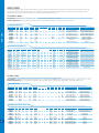
1
Nuvoton Technology Corp. was established as a spin-out of Winbond Electronics’ Logic
business group, starting operation in July, 2008 and completed its IPO in September, 2010.
Nuvoton Technology focuses on R&D and sales in logic ICs, and leads global market shares of
microcontrollers, ISD ChipCorder ®, Speech ICs and computer related application ICs. Nuvoton owns
a six-inch wafer fab, featuring in special niche process. Besides in-house IC products, the wafer
fab also provides part of its capacity for foundry services. Nuvoton Technology provides high cost
performance products for its customers by means of flexible technology innovation capabilities, full
product solutions and excellent integration of technology synergy. Nuvoton offers superior services
based on existing solid foundation and continues to realize its vision: "Be an indispensable partner
to industry leaders." Nuvoton values the long-term relationship with its partners and customers; the
company has established subsidiaries in the USA, China and Israel to strengthen regional customer
support and global management. For more information, please visit www.nuvoton.com.
Nuvoton MCU
Microcontrollers (MCUs) have become very popular and are widely used by all kinds of products,
from low-cost consumer gizmos to highly sophisticated industrial control systems. Recognizing
the demand for increased performance and peripherals, Nuvoton continues to invest significantly
in microcontrollers to provide a broad product portfolio with 8051, ARM7, ARM9, and Cortex™-M0
core, all with rich on-chip peripherals to meet the needs of our existing and future customers.
Nuvoton’s microcontroller portfolio comprises three product lines: ARM7/ARM9 MCUs, 32-bit
NuMicro™ MCUs with ARM ® Cortex™-M0, and 8-bit 8051 compatible MCUs, which have been
widely adopted by customers in a variety of applications including touch panels, network equipment,
POS, home appliances, security systems, etc.
Product Line
NuMicro™ Family
1
Development Tools for NuMicro™ Family
5
ARM7 / ARM9 MCU
7
80C51 MCU
8
Features of NuMicro™ Famlily
11
NuMicro™ Family
NuMicro™ is Nuvoton's brand-new 32-bit Microcontroller (MCU) family powered by the ARM ® Cortex™-M0 processor - the smallest, lowest power and
most energy-efficient ARM processor optimized for a variety of MCU applications. Nuvoton’s NuMicro™ family, which is ready for mass-production
now, includes NUC100 series, NUC120/122/123 series with USB full-speed 2.0 device, NUC130/140 series embedded with Controller Area Network
(CAN) 2.0B licensed from BOSCH, M051 series, Mini51 series, and Nano100 Ultra-low Power series targeting at battery powered applications. With a
variety of product offerings, the NuMicro™ family is ideal for use in industrial control systems, industrial automation, consumer products, embedded
network control, energy, power systems, motor control, and many more. Moreover, with the integration of the industry leading ARM ® Cortex™-M0
microprocessor, the NuMicro™ family brings 32-bit performance at a cost equivalent to traditional 8-bit microcontrollers.
NUC100 Series
The NuMicro™ NUC100 series embedded with the ARM ® Cortex™-M0 core runs up to 72 MHz with 32K/64K/128K bytes Flash Program memory,
4K/8K/16K/20K bytes SRAM, and 4K bytes Flash loader memory for In System Programming (ISP). The NUC100 series also comes equipped with a
variety of peripherals, such as GPIOs, Timers, Watchdog Timer, RTC, PDMA, UART, SPI/MICROWIRE, I 2C, I 2S, PWM, LIN, CAN, PS/2, USB 2.0 FS
Device, 12-bit ADC, Analog Comparator, Low Voltage Reset and Brown-out Detector.
NUC100 Advanced Line
Part No.
Flash SRAM
tData Flash
ISP
ROM
I/O
Timer
Connectivity
UART
SPI
I2C
USB
LIN
I2S
CAN
PWM
ADC
Comp.
RTC
EBI
ISO7816-3
PDMA
ICP
ISP,IAP
IRC
22MHz
Package
NuMicro™ Family
Key Features: Operable at 2.5V to 5.5V and -40°C to +85°C with separate Program Flash (32 KB ~ 128 KB), Data Flash* (4 KB) and ISP loader (4 KB)
and PDMA (*: 128 KB version configurable)
Potential Applications: Industrial Control, Security System, Motor Control, Communication System, e tc.
Low Density
NUC100LC1DN
32K
4K
4K
4K
37
4x32-bit
2
1
2
-
-
-
1
4x16-bit
8x12-bit
1
√
-
9
√
√
√
LQFP48
NUC100LD1DN
64K
4K
4K
4K
37
4x32-bit
2
1
2
-
-
-
1
4x16-bit
8x12-bit
1
√
-
9
√
√
√
LQFP48
NUC100LD2DN
64K
8K
4K
4K
37
4x32-bit
2
1
2
-
-
-
1
4x16-bit
8x12-bit
1
√
-
9
√
√
√
LQFP48
NUC100RC1DN
32K
4K
4K
4K
51
4x32-bit
2
2
2
-
-
-
1
4x16-bit
8x12-bit
2
√
√
9
√
√
√
LQFP64
NUC100RD1DN
64K
4K
4K
4K
51
4x32-bit
2
2
2
-
-
-
1
4x16-bit
8x12-bit
2
√
√
9
√
√
√
LQFP64
NUC100RD2DN
64K
8K
4K
4K
51
4x32-bit
2
2
2
-
-
-
1
4x16-bit
8x12-bit
2
√
√
9
√
√
√
LQFP64
Medium Density
NUC100LD3DN
64K
16K
4K
4K
37
4x32-bit
2
1
2
-
-
-
1
6x16-bit
8x12-bit
1
√
-
9
√
√
√
LQFP48
NUC100LE3DN
128K
16K
Configurable
4K
37
4x32-bit
2
1
2
-
-
-
1
6x16-bit
8x12-bit
1
√
-
9
√
√
√
LQFP48
NUC100RD3DN
64K
16K
4K
4K
51
4x32-bit
3
2
2
-
-
-
1
6x16-bit
8x12-bit
2
√
√
9
√
√
√
LQFP64
NUC100RE3DN
128K
16K
Configurable
4K
51
4x32-bit
3
2
2
-
-
-
1
6x16-bit
8x12-bit
2
√
√
9
√
√
√
LQFP64
NUC100VD2DN
64K
8K
4K
4K
84
4x32-bit
3
4
2
-
-
-
1
8x16-bit
8x12-bit
2
√
√
9
√
√
√
LQFP100
NUC100VD3DN
64K
16K
4K
4K
84
4x32-bit
3
4
2
-
-
-
1
8x16-bit
8x12-bit
2
√
√
9
√
√
√
LQFP100
NUC100VE3DN
128K
16K
Configurable
4K
84
4x32-bit
3
4
2
-
-
-
1
8x16-bit
8x12-bit
2
√
√
9
√
√
√
LQFP100
Data Flash
ISP
ROM
I/O
Timer
UART
SPI
I2C
USB
LIN
CAN
I2S
PWM
ADC
Comp.
RTC
EBI
PDMA
ISO7816-3
ICP
ISP,IAP
IRC
22MHz
Package
NUC120 USB Line
Part No.
Flash SRAM
Connectivity
Low Density
NUC120LC1DN
32K
4K
4K
4K
33
4x32-bit
2
1
2
1
-
-
1
4x16-bit
8x12-bit
1
√
-
9
√
√
√
LQFP48
NUC120LD1DN
64K
4K
4K
4K
33
4x32-bit
2
1
2
1
-
-
1
4x16-bit
8x12-bit
1
√
-
9
√
√
√
LQFP48
NUC120LD2DN
64K
8K
4K
4K
33
4x32-bit
2
1
2
1
-
-
1
4x16-bit
8x12-bit
1
√
-
9
√
√
√
LQFP48
NUC120RC1DN
32K
4K
4K
4K
47
4x32-bit
2
2
2
1
-
-
1
4x16-bit
8x12-bit
2
√
√
9
√
√
√
LQFP64
NUC120RD1DN
64K
4K
4K
4K
47
4x32-bit
2
2
2
1
-
-
1
4x16-bit
8x12-bit
2
√
√
9
√
√
√
LQFP64
NUC120RD2DN
64K
8K
4K
4K
47
4x32-bit
2
2
2
1
-
-
1
4x16-bit
8x12-bit
2
√
√
9
√
√
√
LQFP64
Medium Density
NUC120LD3DN
64K
16K
4K
4K
33
4x32-bit
2
1
2
1
-
-
1
4x16-bit
8x12-bit
1
√
-
9
√
√
√
LQFP48
NUC120LE3DN
128K
16K
Configurable
4K
33
4x32-bit
2
1
2
1
-
-
1
4x16-bit
8x12-bit
1
√
-
9
√
√
√
LQFP48
NUC120RD3DN
64K
16K
4K
4K
47
4x32-bit
2
2
2
1
-
-
1
6x16-bit
8x12-bit
2
√
-
9
√
√
√
LQFP64
NUC120RE3DN
128K
16K
Configurable
4K
47
4x32-bit
2
2
2
1
-
-
1
6x16-bit
8x12-bit
2
√
-
9
√
√
√
LQFP64
NUC120VD2DN
64K
8K
4K
4K
81
4x32-bit
3
4
2
1
-
-
1
8x16-bit
8x12-bit
2
√
-
9
√
√
√
LQFP100
NUC120VD3DN
64K
16K
4K
4K
81
4x32-bit
3
4
2
1
-
-
1
8x16-bit
8x12-bit
2
√
-
9
√
√
√
LQFP100
NUC120VE3DN
128K
16K
Configurable
4K
81
4x32-bit
3
4
2
1
-
-
1
8x16-bit
8x12-bit
2
√
-
9
√
√
√
LQFP100
UART
SPI
I2C
USB
LIN
CAN
NUC122 USB Line (Low Power)
Part No.
Flash
SRAM Data Flash ISP ROM
NUC122ZC1AN
32K
4K
4K
NUC122ZD2AN
64K
8K
4K
Connectivity
I/O
Timer
4K
18
4x32-bit
1
2
1
1
-
4K
18
4x32-bit
1
2
1
1
-
I2S
Comp.
PWM
ADC
RTC
EBI
PDMA
ISP
ICP
IRC
22MHz
-
-
-
-
-
-
-
-
√
√
QFN33
-
-
-
-
-
-
-
-
√
√
QFN33
Package
NUC122LC1AN
32K
4K
4K
4K
30
4x32-bit
2
2
1
1
-
-
-
-
4x16-bit
-
√
-
-
√
√
LQFP48
NUC122LD2AN
64K
8K
4K
4K
30
4x32-bit
2
2
1
1
-
-
-
-
4x16-bit
-
√
-
-
√
√
LQFP48
NUC122SC1AN
32K
4K
4K
4K
41
4x32-bit
2
2
1
1
-
-
-
-
4x16-bit
-
√
-
-
√
√
LQFP64*
NUC122SD2AN
64K
8K
4K
4K
41
4x32-bit
2
2
1
1
-
-
-
-
4x16-bit
-
√
-
-
√
√
LQFP64*
LQFP64* : 7 x 7mm
Contact us: [email protected]
1
NUC123 USB Line (Low Power)
Part No.
Flash
SRAM
Data Flash
ISP ROM
I/O
Timer
NUC123ZC2AN1
36K
12K
Configurable
4K
20
NUC123ZD4AN0
68K
20K
Configurable
4K
NUC123LC2AN1
36K
12K
Configurable
NUC123LD4AN0
68K
20K
Configurable
NUC123SC2AN1
36K
12K
NUC123SD4AN0
68K
20K
Connectivity
I2S
Comp.
PWM
ADC
RTC
EBI
ISP
ICP
IAP
IRC
22MHz
PDMA
-
1
-
2x16-bit
-
-
-
√
√
6
QFN33
-
-
1
-
2x16-bit
-
-
-
√
√
6
QFN33
1
-
-
1
-
4x16-bit
8x10-bit
-
-
√
√
6
LQFP48
1
-
-
1
-
4x16-bit
8x10-bit
-
-
√
√
6
LQFP48
2
1
-
-
1
-
4x16-bit
8x10-bit
-
-
√
√
6
LQFP64*
2
1
-
-
1
-
4x16-bit
8x10-bit
-
-
√
√
6
UART
SPI
I 2C
USB
LIN
CAN
4x32-bit
1
3
1
1
-
20
4x32-bit
1
3
1
1
4K
36
4x32-bit
2
3
2
4K
36
4x32-bit
2
3
2
Configurable
4K
47
4x32-bit
2
3
Configurable
4K
47
4x32-bit
2
3
Package
LQFP64*
LQFP64* : 7 x 7mm
NUC130 Automotive Line
Part No.
Flash SRAM
Data Flash
ISP
ROM
I/O
Timer
Connectivity
UART
SPI
I2C
USB
LIN
CAN
I2S
PWM
ADC
Comp.
RTC
EBI
PDMA
ISO7816-3
ICP
ISP
IRC
22MHz
Package
NuMicro™ Family
NUC130LC1CN
32K
4K
4K
4K
35
4x32-bit
3
1
2
-
2
1
1
4x16-bit
8x12-bit
1
√
-
9
-
√
√
LQFP48
NUC130LD2CN
64K
8K
4K
4K
35
4x32-bit
3
1
2
-
2
1
1
4x16-bit
8x12-bit
1
√
-
9
-
√
√
LQFP48
NUC130LE3CN
128K
16K
Configurable
4K
35
4x32-bit
3
1
2
-
2
1
1
4x16-bit
8x12-bit
1
√
-
9
-
√
√
LQFP48
NUC130RC1CN
32K
4K
4K
4K
49
4x32-bit
3
2
2
-
2
1
1
6x16-bit
8x12-bit
2
√
√
9
-
√
√
LQFP64
NUC130RD2CN
64K
8K
4K
4K
49
4x32-bit
3
2
2
-
2
1
1
6x16-bit
8x12-bit
2
√
√
9
-
√
√
LQFP64
NUC130RE3CN
128K
16K
Configurable
4K
49
4x32-bit
3
2
2
-
2
1
1
6x16-bit
8x12-bit
2
√
√
9
-
√
√
LQFP64
NUC130VE3CN
128K
16K
Configurable
4K
80
4x32-bit
3
4
2
-
2
1
1
8x16-bit
8x12-bit
2
√
√
9
-
√
√
LQFP100
NUC140 Connectivity Line
Part No.
Flash SRAM
Data Flash
ISP
ROM
I/O
Timer
Connectivity
UART
SPI
I2C
USB
LIN
CAN
I2S
PWM
ADC
Comp.
RTC
EBI
PDMA
ISO7816-3
ICP
ISP
IRC
22MHz
Package
NUC140LC1CN
32K
4K
4K
4K
31
4x32-bit
2
1
2
1
2
1
1
4x16-bit
8x12-bit
1
√
-
9
-
√
√
LQFP48
NUC140LD2CN
64K
8K
4K
4K
31
4x32-bit
2
1
2
1
2
1
1
4x16-bit
8x12-bit
1
√
-
9
-
√
√
LQFP48
NUC140LE3CN
128K
16K
Configurable
4K
31
4x32-bit
2
1
2
1
2
1
1
4x16-bit
8x12-bit
1
√
-
9
-
√
√
LQFP48
NUC140RC1CN
32K
4K
4K
4K
45
4x32-bit
3
2
2
1
2
1
1
4x16-bit
8x12-bit
2
√
√
9
-
√
√
LQFP64
NUC140RD2CN
64K
8K
4K
4K
45
4x32-bit
3
2
2
1
2
1
1
4x16-bit
8x12-bit
2
√
√
9
-
√
√
LQFP64
NUC140RE3CN
128K
16K
Configurable
4K
45
4x32-bit
3
2
2
1
2
1
1
4x16-bit
8x12-bit
2
√
√
9
-
√
√
LQFP64
NUC140VE3CN
128K
16K
Configurable
4K
76
4x32-bit
3
4
2
1
2
1
1
8x16-bit
8x12-bit
2
√
√
9
-
√
√
LQFP100
NUC200 Series
The NuMicro™ NUC200 series embedded with the ARM ® Cortex™-M0 core runs up to 50 MHz with 32K/64K/128K bytes Flash program memory,
8K/16K bytes SRAM, and 4K bytes Flash loader memory for In System Programming (ISP) and In Application Program (IAP). The NUC200 series also
comes equipped with a variety of peripherals, such as GPIOs, Timers, Watchdog Timer, RTC, PDMA, UART, SPI/MICROWIRE, I 2C, I 2S, PWM, ISO-7816-3
smart card interface, PS/2, USB 2.0 FS Device, 12-bit ADC, Analog Comparator, Low Voltage Reset, and Brown-out Detector.
Key Features: Operable at 2.5V to 5.5V and -40°C to +85°C with separate Program Flash (32 KB ~ 128 KB), Data Flash* (4 KB) and ISP loader (4 KB)
and PDMA (*: 128 KB version configurable)
Potential Applications: Industrial Control, Security System, Motor Control, Communication System, etc.
NUC200 Advanced Line
Part No.
Flash
SRAM
Data Flash
ISP
ROM
I/O
Timer
Connectivity
UART
SPI
I 2C
USB
I2S
PWM
ADC
Comp. RTC PDMA ISO-7816-3
CRC
VBAT
Supply
ICP
IRC
ISP,IAP 22MHz
Package
NUC200LC2AN
32K
8K
4K
4K
35
4x32-bit
2
1
2
-
1
6x16-bit
7x12-bit
1
√
9
2
√
√
√
√
LQFP48
NUC200LD2AN
64K
8K
4K
4K
35
4x32-bit
2
1
2
-
1
6x16-bit
7x12-bit
1
√
9
2
√
√
√
√
LQFP48
NUC200LE3AN
128K
16K
Configurable
4K
35
4x32-bit
2
1
2
-
1
6x16-bit
7x12-bit
1
√
9
2
√
√
√
√
LQFP48
NUC200SC2AN
32K
8K
4K
4K
49
4x32-bit
3
2
2
-
1
6x16-bit
7x12-bit
2
√
9
2
√
√
√
√
LQFP64*
NUC200SD2AN
64K
8K
4K
4K
49
4x32-bit
3
2
2
-
1
6x16-bit
7x12-bit
2
√
9
2
√
√
√
√
LQFP64*
NUC200SE3AN
128K
16K
Configurable
4K
49
4x32-bit
3
2
2
-
1
6x16-bit
7x12-bit
2
√
9
2
√
√
√
√
LQFP64*
NUC200VE3AN
128K
16K
Configurable
4K
83
4x32-bit
3
4
2
-
1
8x16-bit
8x12-bit
2
√
9
3
√
√
√
√
LQFP100
LQFP64* : 7 x 7mm
NUC220 USB Line
Part No.
2
Flash
SRAM
Data Flash
ISP
ROM
I/O
Timer
Connectivity
UART
SPI
I 2C
USB
I 2S
PWM
ADC
Comp. RTC PDMA ISO-7816-3
CRC
VBAT
Supply
ICP
IRC
ISP,IAP 22MHz
Package
NUC220LC2AN
32K
8K
4K
4K
31
4x32-bit
2
1
2
1
1
4x16-bit
7x12-bit
1
√
9
2
√
√
√
√
LQFP48
NUC220LD2AN
64K
8K
4K
4K
31
4x32-bit
2
1
2
1
1
4x16-bit
7x12-bit
1
√
9
2
√
√
√
√
LQFP48
NUC220LE3AN
128K
16K
Configurable
4K
31
4x32-bit
2
1
2
1
1
4x16-bit
7x12-bit
1
√
9
2
√
√
√
√
LQFP48
NUC220SC2AN
32K
8K
4K
4K
45
4x32-bit
2
2
2
1
1
6x16-bit
7x12-bit
2
√
9
2
√
√
√
√
LQFP64*
NUC220SD2AN
64K
8K
4K
4K
45
4x32-bit
2
2
2
1
1
6x16-bit
7x12-bit
2
√
9
2
√
√
√
√
LQFP64*
NUC220SE3AN
128K
16K
Configurable
4K
45
4x32-bit
2
2
2
1
1
6x16-bit
7x12-bit
2
√
9
2
√
√
√
√
LQFP64*
NUC220VE3AN
128K
16K
Configurable
4K
79
4x32-bit
3
4
2
1
1
8x16-bit
8x12-bit
2
√
9
3
√
√
√
√
LQFP100
LQFP64* : 7 x 7mm
Contact us: [email protected]
M051 Series
The NuMicro M051™ series embedded with the ARM ® Cortex™-M0 core runs up to 50 MHz with 8K/16K/32K/64K bytes Flash program memory, 4K
bytes SRAM, and 4K bytes Flash loader memory for In System Programming (ISP). The M051 series also comes equipped with a variety of peripherals,
such as GPIOs, Timers, UART, SPI, I 2C, PWM, ADC, Comparator, Watchdog Timer , Low Voltage Reset, Brown-out Detected Reset, and supports 96-bit
Unique ID and 128-bit Unique Customer ID.
Key Features: Operable at 2.5V to 5.5V and -40°C to +85°C with separate Program Flash (8 KB ~ 64 KB), Data Flash (4 KB) and ISP loader (4 KB)
Potential Applications: Industrial Control, Security System, Communication System, Motor Control, etc.
M051 Base Line
Flash
SRAM
Data Flash
ISP
ROM
I/O
Timer
M052LCN
8K
4K
4K
4K
40
M052ZCN
8K
4K
4K
4K
24
M054LCN
16K
4K
4K
4K
M054ZCN
16K
4K
4K
M058LCN
32K
4K
4K
Connectivity
PWM
ADC
Comp.
EBI
ICP
ISP
IRC
22MHz
Package
2
8x16-bit
8x12-bit
2
√
√
√
LQFP48
2
5x16-bit
5x12-bit
2
-
√
√
QFN33
2
2
8x16-bit
8x12-bit
2
√
√
√
LQFP48
2
1
2
5x16-bit
5x12-bit
2
-
√
√
QFN33
2
2
2
8x16-bit
8x12-bit
2
√
√
√
LQFP48
UART
SPI
I2C
4x32-bit
2
2
4x32-bit
2
1
40
4x32-bit
2
4K
24
4x32-bit
4K
40
4x32-bit
M058ZCN
32K
4K
4K
4K
24
4x32-bit
2
1
2
5x16-bit
5x12-bit
2
-
√
√
QFN33
M0516LCN
64K
4K
4K
4K
40
4x32-bit
2
2
2
8x16-bit
8x12-bit
2
√
√
√
LQFP48
M0516ZCN
64K
4K
4K
4K
24
4x32-bit
2
1
2
5x16-bit
5x12-bit
2
-
√
√
QFN33
NuMicro™ Family
Part No.
Mini51 Series
The NuMicro™ Mini51 series embedded with the ARM ® Cortex™-M0 core runs up to 24 MHz with 4K/8K/16K bytes Flash program memory, 2K bytes
SRAM and 2K bytes Flash loader memory for In System Programming (ISP). The Mini51 series also comes equipped with a variety of peripherals, such
as GPIOs, Timers, UART, SPI, I 2C, PWM, ADC, Comparator, Watchdog Timer, Low Voltage Reset, Brown-out Detected Reset, and supports 96-bit Unique
ID and 128-bit Unique Customer ID.
Key Features: Operable at 2.5V to 5.5V and -40°C to +85°C with separate Program Flash (4 KB ~ 16 KB) and ISP loader (2 KB), RTC, and Internal RC
trimmed to 1% accuracy with external 32K crystal
Potential Applications: Auto-control System, Data Communication, Industrial Control, etc.
Mini51 Base Line
Part No.
Flash
SRAM
Data Flash
ISP
ROM
I/O
Timer
Connectivity
UART
SPI
I2C
PWM
ADC
Comp.
ICP
ISP
IRC
22MHz
Package
LQFP48
MINI51LBN
4K
2K
Configurable
2K
30
2x32-bit
1
1
1
6x16-bit
8x10-bit
2
√
√
MINI51ZBN
4K
2K
Configurable
2K
29
2x32-bit
1
1
1
6x16-bit
8x10-bit
2
√
√
QFN33*
MINI51TBN
4K
2K
Configurable
2K
29
2x32-bit
1
1
1
6x16-bit
8x10-bit
2
√
√
QFN33**
LQFP48
MINI52LBN
8K
2K
Configurable
2K
30
2x32-bit
1
1
1
6x16-bit
8x10-bit
2
√
√
MINI52ZBN
8K
2K
Configurable
2K
29
2x32-bit
1
1
1
6x16-bit
8x10-bit
2
√
√
QFN33*
MINI52TBN
8K
2K
Configurable
2K
29
2x32-bit
1
1
1
6x16-bit
8x10-bit
2
√
√
QFN33**
LQFP48
MINI54LBN
16K
2K
Configurable
2K
30
2x32-bit
1
1
1
6x16-bit
8x10-bit
2
√
√
MINI54ZBN
16K
2K
Configurable
2K
29
2x32-bit
1
1
1
6x16-bit
8x10-bit
2
√
√
QFN33*
MINI54TBN
16K
2K
Configurable
2K
29
2x32-bit
1
1
1
6x16-bit
8x10-bit
2
√
√
QFN33**
QFN33* : 5 x 5mm
QFN33** : 4 x 4mm
Contact us: [email protected]
3
Nano Series
The NuMicro™ Nano series embedded with the ARM ® Cortex™-M0 core runs up to 42 MHz with 32K/64K/128K bytes embedded Flash and 8K/16K bytes
embedded SRAM and 4K bytes loader ROM for In System Programming (ISP). The Nano series integrates the 4x40 or 6x38 COM/SEG LCD controller,
Real Time Counter (RTC), 12-bit SAR ADC, 12-bit DAC, Capacitive Touch-key, UART, SPI, I 2C, I 2S, PWM/Capture, EBI, USB 2.0 FS Device, ISO-7816-3,
Watchdog timer, Brown-out Detector, fast wake-up via all peripheral interfaces and supports 96-bit Unique ID and 128-bit Unique Customer ID.
Key Features: Operable at 1.8V to 3.6V and -40°C to +85°C with ultra-low power: 200 uA/MHz (Normal), 75 uA/MHz (Idle), 2.5 uA (Power Down, RTC,
RAM retention) and 1 uA (Power Down, RAM retention), and less than 7 us wake-up time
Potential Applications: Portable Health Care Device,Mobile Payment Smart Card Reader, Wireless Audio, Motion Gaming, IPTV Remote Control, Smart
Home Appliances, Alarm and Security Monitoring,Zigbee Smart Energy AMR, GPS Data Logger, Car ETC, Home Smart Heat/
Water/Gas Meter, etc.
Nano100 Base Line (Ultra Low Power)
Part No.
Flash SRAM
Data Flash
ISP
ROM
I/O
Connectivity
Timer
UART
I2C
SPI
USB
I 2S
12-bit
ADC
PWM
RTC
IRC
10KHz
12MHz
EBI
PDMA
LCD
12-bit
DAC
ISO7816-3
Touch
Key
ISP
ICP
Package
NuMicro™ Family
NANO100LC2BN
32K
8K
Configurable
4K
38
4x32-bit
4
3
2
-
1
6
7
√
-
√
8
-
2
2
4
√
LQFP48
NANO100LD2BN
64K
8K
Configurable
4K
38
4x32-bit
4
3
2
-
1
6
7
√
-
√
8
-
2
2
4
√
LQFP48
NANO100LD3BN
64K
16K
Configurable
4K
38
4x32-bit
4
3
2
-
1
6
7
√
-
√
8
-
2
2
4
√
LQFP48
NANO100LE3BN
128K
16K
Configurable
4K
38
4x32-bit
4
3
2
-
1
6
7
√
-
√
8
-
2
2
4
√
LQFP48
NANO100SC2BN
32K
8K
Configurable
4K
52
4x32-bit
5
3
2
-
1
8
7
√
-
√
8
-
2
3
8
√
LQFP64*
NANO100SD2BN
64K
8K
Configurable
4K
52
4x32-bit
5
3
2
-
1
8
7
√
-
√
8
-
2
3
8
√
LQFP64*
NANO100SD3BN
64K
16K
Configurable
4K
52
4x32-bit
5
3
2
-
1
8
7
√
-
√
8
-
2
3
8
√
LQFP64*
NANO100SE3BN
128K
16K
Configurable
4K
52
4x32-bit
5
3
2
-
1
8
7
√
-
√
8
-
2
3
8
√
LQFP64*
NANO100KC2BN
32K
8K
Configurable
4K
86
4x32-bit
5
3
2
-
1
8
12
√
√
√
8
-
2
3
16
√
LQFP128**
NANO100KD2BN
64K
8K
Configurable
4K
86
4x32-bit
5
3
2
-
1
8
12
√
√
√
8
-
2
3
16
√
LQFP128**
NANO100KD3BN
64K
16K
Configurable
4K
86
4x32-bit
5
3
2
-
1
8
12
√
√
√
8
-
2
3
16
√
LQFP128**
NANO100KE3BN
128K
16K
Configurable
4K
86
4x32-bit
5
3
2
-
1
8
12
√
√
√
8
-
2
3
16
√
LQFP128**
LQFP64* : 7 x 7mm
LQFP128** : 14 x 14mm
Nano110 LCD Line (Ultra Low Power)
Part No.
Flash SRAM
Data Flash
ISP
ROM
I/O
Timer
Connectivity
UART SPI
I2C
USB
I2 S
12-bit
ADC
PWM
RTC
IRC
10KHz
12MHz
EBI
PDMA
12-bit
DAC
LCD
ISO7816-3
Touch
Key
ISP
ICP
Package
LQFP64*
NANO110SC2BN
32K
8K
Configurable
4K
51
4x32-bit
5
3
2
-
1
7
7
√
-
√
8
4x31, 6x29
2
3
8
√
NANO110SD2BN
64K
8K
Configurable
4K
51
4x32-bit
5
3
2
-
1
7
7
√
-
√
8
4x31, 6x29
2
3
8
√
LQFP64*
NANO110SD3BN
64K
16K
Configurable
4K
51
4x32-bit
5
3
2
-
1
7
7
√
-
√
8
4x31, 6x29
2
3
8
√
LQFP64*
NANO110SE3BN
128K
16K
Configurable
4K
51
4x32-bit
5
3
2
-
1
7
7
√
-
√
8
4x31, 6x29
2
3
8
√
LQFP64*
NANO110KC2BN
32K
8K
Configurable
4K
86
4x32-bit
5
3
2
-
1
8
12
√
√
√
8
4x40, 6x38
2
3
16
√
LQFP128**
NANO110KD2BN
64K
8K
Configurable
4K
86
4x32-bit
5
3
2
-
1
8
12
√
√
√
8
4x40, 6x38
2
3
16
√
LQFP128**
NANO110KD3BN
64K
16K
Configurable
4K
86
4x32-bit
5
3
2
-
1
8
12
√
√
√
8
4x40, 6x38
2
3
16
√
LQFP128**
NANO110KE3BN
128K
16K
Configurable
4K
86
4x32-bit
5
3
2
-
1
8
12
√
√
√
8
4x40, 6x38
2
3
16
√
LQFP128**
LQFP64* : 7 x 7mm
LQFP128** : 14 x 14mm
Nano120 USB Connectivity Line (Ultra Low Power)
Connectivity
I 2S
PWM
12-bit
ADC
RTC
EBI
IRC
10KHz
12MHz
PDMA
LCD
12-bit
DAC
ISO7816-3
Touch
Key
ISP
ICP
Package
1
1
4
7
√
-
√
8
-
2
2
4
√
LQFP48
1
1
4
7
√
-
√
8
-
2
2
4
√
LQFP48
2
1
1
4
7
√
-
√
8
-
2
2
4
√
LQFP48
3
2
1
1
4
7
√
-
√
8
-
2
2
4
√
LQFP48
5
3
2
1
1
8
7
√
-
√
8
-
2
3
8
√
LQFP64*
5
3
2
1
1
8
7
√
-
√
8
-
2
3
8
√
LQFP64*
4x32-bit
5
3
2
1
1
8
7
√
-
√
8
-
2
3
8
√
LQFP64*
48
4x32-bit
5
3
2
1
1
8
7
√
-
√
8
-
2
3
8
√
LQFP64*
4K
86
4x32-bit
5
3
2
1
1
8
8
√
√
√
8
-
2
3
8
√
LQFP128**
Configurable
4K
86
4x32-bit
5
3
2
1
1
8
8
√
√
√
8
-
2
3
16
√
LQFP128**
Configurable
4K
86
4x32-bit
5
3
2
1
1
8
8
√
√
√
8
-
2
3
16
√
LQFP128**
Configurable
4K
86
4x32-bit
5
3
2
1
1
8
8
√
√
√
8
-
2
3
16
√
LQFP128**
Part No.
Flash
SRAM
Data Flash
ISP
ROM
I/O
Timer
NANO120LC2BN
32K
8K
Configurable
4K
34
4x32-bit
4
NANO120LD2BN
64K
8K
Configurable
4K
34
4x32-bit
4
NANO120LD3BN
64K
16K
Configurable
4K
34
4x32-bit
NANO120LE3BN
128K
16K
Configurable
4K
34
NANO120SC2BN
32K
8K
Configurable
4K
NANO120SD2BN
64K
8K
Configurable
4K
NANO120SD3BN
64K
16K
Configurable
NANO120SE3BN
128K
16K
NANO120KC2BN
32K
NANO120KD2BN
NANO120KD3BN
NANO120KE3BN
I2C
USB
3
2
3
2
4
3
4x32-bit
4
48
4x32-bit
48
4x32-bit
4K
48
Configurable
4K
8K
Configurable
64K
8K
64K
16K
128K
16K
UART SPI
LQFP64* : 7 x 7mm
LQFP128** : 14 x 14mm
Nano130 Advanced Line (Ultra Low Power)
4
Connectivity
I 2S
PWM
12-bit
ADC
RTC
EBI
IRC
10KHz
12MHz
PDMA
LCD
12-bit
DAC
ISO7816-3
Touch
Key
ISP
ICP
Package
1
1
7
7
√
-
√
8
4x31,6x29
2
3
8
√
LQFP64*
1
1
7
7
√
-
√
8
4x31,6x29
2
3
8
√
LQFP64*
2
1
1
7
7
√
-
√
8
4x31,6x29
2
3
8
√
LQFP64*
3
2
1
1
7
7
√
-
√
8
4x31,6x29
2
3
8
√
LQFP64*
5
3
2
1
1
8
8
√
√
√
8
4x40,6x38
2
3
16
√
LQFP128**
4x32-bit
5
3
2
1
1
8
8
√
√
√
8
4x40,6x38
2
3
16
√
LQFP128**
4x32-bit
5
3
2
1
1
8
8
√
√
√
8
4x40,6x38
2
3
16
√
LQFP128**
4x32-bit
5
3
2
1
1
8
8
√
√
√
8
4x40,6x38
2
3
16
√
LQFP128**
Part No.
Flash
SRAM
Data Flash
ISP
ROM
I/O
Timer
NANO130SC2BN
32K
8K
Configurable
4K
47
4x32-bit
5
NANO130SD2BN
64K
8K
Configurable
4K
47
4x32-bit
5
NANO130SD3BN
64K
16K
Configurable
4K
47
4x32-bit
NANO130SE3BN
128K
16K
Configurable
4K
47
NANO130KC2BN
32K
8K
Configurable
4K
NANO130KD2BN
64K
8K
Configurable
NANO130KD3BN
64K
16K
Configurable
NANO130KE3BN
128K
16K
Configurable
I2C
USB
3
2
3
2
5
3
4x32-bit
5
86
4x32-bit
4K
86
4K
86
4K
86
UART SPI
LQFP64* : 7 x 7mm
LQFP128** : 14 x 14mm
Contact us: [email protected]
Development Tools for NuMicro™ Family
▪ IAR EWARM / Keil RVMDK available on IAR / Keil website
▪ Support CooCox CoIDE
▪ Support On-line ICP (In-Circuit Programming)
Development Tools for NuMicro™ Family
SDK (Software Development Kit)
Ordering No.
NuTiny-SDK-Mini51
NuTiny-SDK-M051
NuTiny-SDK-NUC100
NuTiny-SDK-NUC122
NuTiny-SDK-NUC123
NuTiny-SDK-NUC140
NuTiny-SDK-NUC200
NuTiny-SDK-NUC220
NuTiny-SDK-Nano100
NuTiny-SDK-Nano120
NuTiny-SDK-Nano130
▪ NuTiny-EVB-Mini51
▪ USB Cable
▪ Nu-Link-ME
▪ NuTiny-EVB-M051
▪ USB Cable
▪ Nu-Link-ME
▪ NuTiny-EVB-NUC100
Supported Device
Mini51
Mini52
Mini54
Mini51 Series by Mini54LAN
M052
M054
M058
M0516
M051 Series by M0516LBN
NUC100
NUC100 Series by NUC100LE3AN
NUC120
NUC120 Series by NUC120LE3AN
NUC122
NUC122 Series by NUC122SD2AN
NUC123
NUC123 Series by NUC123SD4AN0
NUC130
NUC140
NUC130/140 Series by NUC140VE3CN
NUC200
NUC200 Series by NUC200VE3AN
NUC220
NUC220 Series by NUC220VE3AN
Nano100
Nano100 Series by Nano100KE3BN
▪ NuTiny-EVB-Nano120
Nano120
Nano120 Series by Nano120KE3BN
▪ Nu-Link-ME
▪ NuTiny-EVB-Nano130
▪ LCD Module
▪ USB Cable
Nano110
Nano130
Nano130 Series by Nano130KE3BN
▪ USB Cable
▪ Nu-Link-ME
▪ NuTiny-EVB-NUC120
▪ USB Cable
▪ Nu-Link-ME
▪ NuTiny-EVB-NUC122
▪ USB Cable
▪ Nu-Link-ME
▪ NuTiny-EVB-NUC123
▪ USB Cable
▪ Nu-Link-ME
▪ NuTiny-EVB-NUC140
▪ USB Cable
▪ Nu-Link-ME
▪ NuTiny-EVB-NUC200
▪ USB Cable
▪ Nu-Link-ME
▪ NuTiny-EVB-NUC220
▪ USB Cable
▪ Nu-Link-ME
▪ NuTiny-EVB-Nano100
▪ USB Cable
▪ Nu-Link-ME
▪ USB Cable
Content
▪ Nu-LB-NUC140
Nu-LB-NUC140
▪ Nu-Link-ME on board
▪ USB Cable ▪ NuMicro Family CD
▪ Nu-LB-M051
Nu-LB-M051
▪ Nu-Link-ME on board
▪ USB Cable
▪ NuMicro Family CD
▪ Nu-LB-Mini51
Nu-LB-Mini51
▪ Nu-Link-ME on board
▪ USB Cable ▪ NuMicro Family CD
▪ Nu-LB-Nano130
Nu-LB-Nano130
Picture
▪ A Starter Kit made by Nuvoton
▪ IAR EWARM (evaluation version) and Keil RVMDK (evaluation version) included
▪ Support CooCox CoIDE
▪ Examples with source code included
Learning Board (LB)
Ordering No.
Evaluation / Development Kit for
Development Tools for NuMicro™ Family
NuTiny-SDK-NUC120
Content
▪ Nu-Link-ME
▪ Nu-Link-ME on board
▪ LCD Module
▪ USB Cable
▪ NuMicro Family CD
Supported Device
NUC100
NUC120
NUC130
NUC140
M052
M054
M058
M0516
Mini51
Mini52
Mini54
Nano100
Nano110
Nano120
Nano130
Evaluation / Development Kit for
Picture
▪ SD Card
▪ USB
▪ CAN &LIN
▪ EEPROM & Flash Memory
▪ Display
▪ Audio via NAU8822
▪ EEPROM & Flash Memory
▪ Display
▪ EBI Interface
▪ EEPROM & Flash Memory
▪ Display
▪ SD Card
▪ USB
▪ Touck Key
▪ 3.5" TFT Color Display
▪ Smart Card Reader
▪ Audio via NAU8822
Nu-Link
Ordering No.
Nu-Link
Nu-Link-Pro
Content
▪ Nu-Link
▪ Nu-Link-Pro
Supported Device
Description
NuMicro Family
▪ USB←→SWD bridge
▪ Support On-line and Off-line ICP (In-Circuit Programming)
▪ USB Plug & Play
NuMicro Family
▪ USB←→SWD bridge
▪ Support On-line and Off-line ICP (In-Circuit Programming)
▪ USB Plug & Play
▪ Programmable output VDD: 1.8V,2.5V,3.3V,5.0V
▪ Wide target VDD input level:1.8V~5.5V
Picture
5
Contact us: [email protected]
Development Tools for NuMicro™ Family
Ordering No.
Content
Supported Devices
Description
Picture
3rd Party Starter Kit (SKT)
Nu-IAR-SKT
▪ NUC140-SK
▪ USB Cable ▪ NuMicro Family CD
▪ U-LINK-ME
Nu-Keil-SKT
▪ MCBNUC1XX
▪ USB Cable ▪ NuMicro Family CD
NUC100
NUC120
NUC130
NUC140
▪ Starter Kit made by IAR
▪ IAR EWARM (evaluation version) included
▪ IAR C/C++ Compiler included
▪ USB Plug & Play
NUC100
NUC120
NUC130
NUC140
▪ Starter Kit made by Keil
▪ Keil RVMDK (evaluation version) included
▪ ARM C/C++ Compiler included
▪ USB Plug & Play
NuMicro Mini51 Series Gang Writer (NuGang)
NuGang-Mini51T-QFN33
NuGang-Mini51Z-QFN33
Development Tools for NuMicro™ Family
NuGang-Mini51L-QFN33
▪ User Manual
▪ 4-chip Gang Programming Board
▪ USB Cable
▪ User Manual
▪ 4-chip Gang Programming Board
▪ USB Cable
▪ User Manual
▪ 4-chip Gang Programming Board
▪ USB Cable
Mini51T
Mini52T
Mini54T
Mini51Z
Mini52Z
Mini54Z
Mini51L
Mini52L
Mini54L
▪ Support Mini51 series 4 chips at one time
▪ USB to PC/Laptop interface
▪ Support Off-line copy function
* T: QFN33 4x4mm
* Z: QFN33 5x5mm
* L: LQFP48 7x7mm
NuMicro M051 Series Gang Writer (NuGang)
NuGang-M051Z-QFN33
NuGang-M051L-LQFP48
▪ User Manual
▪ 4-chip Gang Programming Board
▪ USB Cable
▪ User Manual
▪ 4-chip Gang Programming Board
▪ USB Cable
M052Z
M054Z
M058Z
M0516Z
M052L
M054L
M058L
M0516L
▪ Support M051 series 4 chips at one time
▪ USB to PC/Laptop interface
▪ Support Off-line copy function
* Z: QFN33 5x5mm
* L: LQFP48 7x7mm
NuMicro NUC100 Series Gang Writer (NuGang)
NuGang-NUC100L-LQFP48
NuGang-NUC100R-LQFP64
NuGang-NUC100V-LQFP100
NuGang-NUC122Z-QFN33
NuGang-NU122L-LQFP48
NuGang-NUC122S-LQFP64
NuGang-NUC123Z-QFN33
NuGang-NU123L-LQFP48
NuGang-NUC123S-LQFP64
▪ User Manual
▪ 4-chip Gang Programming Board
▪ USB Cable
▪ User Manual
▪ 4-chip Gang Programming Board
▪ USB Cable
NUC100L
NUC120L
NUC130L
NUC140L
NUC100R
NUC120R
NUC130R
NUC140R
▪ 4-chip Gang Programming Board
NUC100V
NUC120V
NUC130V
NUC140V
▪ User Manual
▪ 4-chip Gang Programming Board
▪ USB Cable
NUC122Z
▪ User Manual
▪ USB Cable
▪ User Manual
▪ 4-chip Gang Programming Board
▪ USB Cable
▪ User Manual
▪ 4-chip Gang Programming Board
▪ USB Cable
▪ User Manual
▪ 4-chip Gang Programming Board
▪ USB Cable
▪ User Manual
▪ 4-chip Gang Programming Board
▪ USB Cable
▪ User Manual
▪ 4-chip Gang Programming Board
▪ USB Cable
▪ Support NUC100 series 4 chips at one time
▪ USB to PC/Laptop interface
▪ Support Off-line copy function
NUC122L
* Z: QFN33 5x5mm
* L: LQFP48 7x7mm
* S: LQFP64 7x7mm
* R: LQFP64 10x10mm
NUC122S
* V: LQFP100 14x14mm
NUC123Z
NUC123L
NUC123S
NuMicro NUC200 Series Gang Writer (NuGang)
NuGang-NUC200L-LQFP48
NuGang-NUC200S-LQFP64
NuGang-NUC200V-LQFP100
▪ User Manual
▪ 4-chip Gang Programming Board
▪ USB Cable
▪ User Manual
▪ 4-chip Gang Programming Board
▪ USB Cable
▪ User Manual
▪ 4-chip Gang Programming Board
▪ USB Cable
NUC200L
NUC220L
▪ Support NUC200 series 4 chips at one time
▪ USB to PC/Laptop interface
NUC200S
NUC220S
▪ Support Off-line copy function
* L: LQFP48 7x7mm
* S: LQFP64 7x7mm
NUC200V
NUC220V
* V: LQFP100 14x14mm
NuMicro Nano100 Series Gang Writer (NuGang)
NuGang-Nano100L-LQFP48
NuGang-Nano100S-LQFP64
6
NuGang-Nano100K-LQFP128
▪ User Manual
▪ 4-chip Gang Programming Board
▪ USB Cable
▪ User Manual
▪ 4-chip Gang Programming Board
▪ USB Cable
▪ User Manual
▪ 4-chip Gang Programming Board
▪ USB Cable
Nano100L
Nano120L
▪ Support Nano100 series 4 chips at one time
Nano100S
Nano110S
Nano120S
Nano130S
▪ USB to PC/Laptop interface
Nano100K
Nano110K
Nano120K
Nano130K
* K: LQFP128 14x14mm
▪ Support Off-line copy function
* L : LQFP48 7x7mm
* S: LQFP64 7x7mm
Contact us: [email protected]
ARM7 / ARM9 MCU
Nuvoton provides a series of network connected processors with feature rich peripherals based on ARM7TDMI and ARM926 to let customers implement
their innovative products in a timely manner. A complete development environment is provided for each platform. The source code of BSP drivers under
Linux/WinCE are all provided to shorten the design cycle times. The targeted applications range from devices that require network connectivity, USB
connectivity, user interface devices, and industrial control, such as POS, HMI, IP camera, industrial control, etc. The NUC501 is an ARM7TDMI-based
MCU, specifically designed to offer low cost and high performance for various applications, such as 2.4G RF wireless applications, thermal printer,
barcode reader, and home appliances.
NUC ARM
Memory
I/F
Core
GFX
LCD
Timer
Analog
Peripheral
JTAG
External Bus Interface
GPIO (Max)
UART
I2C
SPI
KPI
PS2
I2S/AC97
PCI Master
√
4
8
400K
-
1
√
√
-
26
37
1
2
1
2
-
-
-
-
1.8 3.3
√
E
LQFP-48
LQFP-64
NUC710A
80
ARM7TDMI
4
4
-
-
√
√
1
-
-
1
1
2
-
1
-
-
√
√
√
4
-
-
-
-
-
√
√
71
4
2
1
√
1
1
-
1.8 3.3
-
I
LQFP-176
NUC740A
80
ARM7TDMI
8
2
-
-
√
√
-
-
-
-
2
1
-
-
-
-
-
-
-
-
-
-
-
-
-
√
√
21
1
-
-
-
-
-
-
1.8 3.3
-
C
LQFP-176
NUC745A
80
ARM7TDMI
4
4
-
-
√
√
1
-
-
-
1
2
-
1
-
-
-
-
-
4
-
-
-
-
-
√
√
31
4
2
1
√
1
1
-
1.8 3.3
-
I
LQFP-128
NUC910A
200
ARM926EJ
8
8
-
-
√
√
1
4
√
2
1
-
2
-
1
√
-
√
√
4
8
300K
√
-
√
√
√
92
5
2
1
√
2
1
-
1.8 3.3
-
I
PBGA-324
NUC920A
200
ARM926EJ
8
8
-
-
√
√
1
-
√
1
1
-
2
-
1
-
-
-
√
4
8
300K
√
-
√
√
√
92
3
2
1
√
2
1
3
1.8 3.3
-
I
PBGA-324
NUC945A
200
ARM926EJ
8
8
-
-
√
√
-
-
-
1
1
-
1
-
1
-
-
-
-
-
-
-
-
-
-
√
√
34
1
-
-
-
-
-
-
1.8 3.3
-
C
LQFP-128
NUC946A
200
ARM926EJ
8
8
-
-
√
√
√
-
-
1
1
-
2
-
1
-
-
-
-
-
-
-
-
-
-
√
√
37
2
2
1
-
-
-
-
1.8 3.3
-
I2
LQFP-128
NUC950A
200
ARM926EJ
8
8
-
-
√
√
1
4
-
1
1
-
2
-
1
√
-
√
-
4
-
-
-
-
-
√
√
52
3
2
1
√
-
1
-
1.8 3.3
-
I2
LQFP-216
NUC951A
200
ARM926EJ
8
8
-
-
√
√
√
4
-
2
1
-
2
-
1
√
-
√
√
4
-
-
-
-
-
√
√
63
3
2
1
√
√
1
-
1.8 3.3
-
I2
LQFP-216
NUC960A
200
ARM926EJ
8
8
-
-
√
√
1
-
-
-
1
-
2
-
1
-
-
-
-
-
-
-
-
-
-
√
√
51
3
2
1
-
-
-
2
1.8 3.3
-
I2
LQFP-216
*NUC970A
300
ARM926EJ
16 16 32
√
√
√
1
24
-
1
2
-
2
-
1
√
-
√
√
4
8
1M
√
-
√
√
√
?
8
2
2
√
-
√
-
1.2 3.3
-
I
LQFP-216
ARM7 / ARM9 MCU
LVD/LVR
-
Package
16-bit DAC Channels
-
Built-in LDO
Touch Screen Controller
-
Package
Operating Temperature 1
Speed (Samples per
second)
-
I/O Voltage (V)
PWM
No. of Channels
1
Core Voltage (V)
TFT LCD
Real-Time Clock (RTC)
-
STN LCD
-
2D Graphics
-
USB 2.0 FS Device
-
Power
USB 2.0 HS Device
-
USB 2.0 Host (480M bps)
-
Ethernet 10/100 MAC
2
USB 1.1 Host (12M bps)
-
ATAPI
-
SD / SDIO
√
USB
ADC (10-bit)
SPI Flash, No. of I/O Pins
32
MAC
NAND Flash, No. of ECC bits
-
SDRAM
-
NOR Flash
SRAM (KB)
Security against piracy
ARM7TDMI
I Cache (KB)
80
D Cache (KB)
CPU
NUC501A/B
Max Speed (MHz)
Part No.
Storage
*Under development, available in 2Q, 2013.
1. Commercial (C) is 0 to +70ºC, Industrial (I) is -40 to +85 ºC, Extended (E) is -40 to +105 ºC.
2. VDD18 for IO Buffer: 1.8V+/-10%, VDD33 for Core Logic: 3.3V+/-5%, USBVDDC0/USBVDDC1/USBVDDT0/USBVDDT1 for USB: 3.3V+/-5%, PLLVDD18 for PLL: 1.8V+/-10%
ARM Development Tools
ARM7
Part No.
NUC740
NUC710
NUC745
NUC501
SDK
ARM ADS 1.2
ARM ADS 1.2
ARM ADS 1.2
ARM ADS 1.2 / Keil / IAR / GNU
uClinux
uClinux 2.4.20
uClinux 2.6.38
uClinux 2.6.38
Driver Library, Driver Sample Code,
USB Device Samples, PLL Generator Tool,
Writer Tool, User's Manual, Quick Start Guide,
Application Note
Part No.
NUC910
NUC945/946
NUC950/951
NUC960
SDK
ARM ADS 1.2
ARM ADS 1.2
ARM ADS 1.2
ARM ADS 1.2
ARM9
WinCE 5.0 / 6.0 BSP
√
-
√
-
Linux
Linux 2.6.17
Linux 2.6.35
Linux 2.6.17
Linux 2.6.35
Linux 2.6.17
Linux 2.6.35
Linux 2.6.17
Linux 2.6.35
Contact us: [email protected] 7
80C51 MCU
As a leading supplier of 8051 microcontrollers (MCUs), Nuvoton offers a variety of products with the best-in-class price/performance critical to the
success of consumers and industrial products. The 8-bit MCU comes equipped with rich peripherals to meet various system requirements and is
supported by the tool chain from word leading tool makers for rapid product development.
6T/12T 80C51 Series
Key Features: Operable at 2.4V ~ 5.5V and -40°C ~ +85°C with UART, SPI, Internal RC and ISP
Potential Applications: Bar Code Reader, Key Phone, KVM, 2.4G Wireless Keyboard, IPC, Monitor, Security System,etc.
W78 Standard Line
Part No.
Flash
SRAM
ISP Loader
ROM
I/O
Timer
W78E052D
8K
256
2K
36
3x16-bit
Connectivity
UART
SPI
I 2C
1
-
-
80C51 MCU
Comp.
PWM
ADC
INT
ISP
ICP
Special Function
Package
-
-
-
4
ISP
6T/12T option, Extra I/O port
PDIP40/PLCC44/PQFP44/LQFP48
PDIP40/PLCC44/PQFP44/LQFP48
W78E054D
16K
256
2K
36
3x16-bit
1
-
-
-
-
-
4
ISP
6T/12T option, Extra I/O port
W78E058D
32K
512
4K
36
3x16-bit
1
-
-
-
-
-
4
ISP
6T/12T option, Extra I/O port
PDIP40/PLCC44/PQFP44/LQFP48
W78E516D
64K
512
4K
36
3x16-bit
1
-
-
-
-
-
4
ISP
6T/12T option, Extra I/O port
PDIP40/PLCC44/PQFP44/LQFP48
W78ERD2A
64K
256+1K
4K
36
3x16-bit
1
-
-
-
5x8-bit
-
4
ISP
PCA, 6T/12T option, Extra I/O port
PDIP40/PLCC44/PQFP44
W78E858A
32K
768
4K
36
3x16-bit
1
-
-
-
4x8-bit
-
10
ISP
128B EE, Extra I/O port
PDIP40/PLCC44/PQFP44
W78C032
-
256
-
32
3x16-bit
1
-
-
-
-
-
2
-
Extra I/O port
PDIP40/PLCC44/PQFP44
W78C438
-
256
-
40
3x16-bit
1
-
-
-
-
-
4
-
1MB external memory space
PQFP100
N78/W78 Industrial Line
Part No.
Flash
SRAM
Data
Flash
ISP Loader
ROM
I/O
Timer
*N78S052
8K
256+1K
8K
2K
46
*N78S054
16K
256+1K
Share AP ROM
2K
46
N78E055A
N78E059A
16K
32K
256+1K
4K
256+1K
2.5K
4K
40
2.5K
Connectivity
PWM
ADC
INT
ISP
ICP
Special Function
Package
1
-
5x8-bit
-
4
ISP
6T/12T option, Extra I/O port,
internal 22MHz RC, 2 level BOR
PDIP40/PLCC44/PQFP44/LQFP48
1
-
5x8-bit
-
4
ISP
6T/12T option, Extra I/O port,
internal 22MHz RC, 2 level BOR
PDIP40/PLCC44/PQFP44/LQFP48
ISP
6T/12T option, Extra I/O port,
internal 22MHz RC, 4 level BOR
PDIP40/PLCC44/PQFP44/LQFP48
ISP
6T/12T option, Extra I/O port,
internal 22MHz RC, 4 level BOR
PDIP40/PLCC44/PQFP44/LQFP48
PDIP40/PLCC44/PQFP44/LQFP48
SPI
I 2C
4x16-bit
2
1
4x16-bit
2
1
3x16-bit
40
Comp.
UART
1
3x16-bit
1
1
-
1
-
-
5x8-bit
-
-
5x8-bit
4
-
4
N78E517A
64K
256+1K
Share AP ROM
2.5K
40
3x16-bit
1
1
-
-
5x8-bit
-
4
ISP
6T/12T option, Extra I/O port,
internal 22MHz RC, 4 level BOR
N78E366A
64K
256+1K
-
2.5K
40
3x16-bit
1
1
-
-
5x8-bit
-
4
ISP
6T/12T option, Extra I/O port,
internal 22MHz RC, 4 level BOR
PDIP40/PLCC44/PQFP44/LQFP48
W78IRD2A
64K
256+1K
-
4K
36
3x16-bit
1
-
-
-
5x8-bit
-
4
ISP
PCA, 6T/12T option, Extra I/O port
PDIP40/PLCC44
*Under development, available in 2Q, 2013.
4T 80C51 Series
Key Features: 4T 80C52 Core integrated with Data Flash, 2* I²C, 2* UART, SPI, PWM(QEI), ADC and ISP operating at 2.4V ~ 5.5V and -40℃ ~ +85℃
Potential Applications: IPC, Communication Equipment, Security/Alarm System, LCD TV, Motor Applications, Power Management, etc.
W77 Turbo Line
Part No.
Flash
SRAM
ISP Loader
ROM
I/O
Timer
W77E058A
32K
256+1K
-
36
3x16-bit
Connectivity
UART
SPI
I 2C
2
-
-
Comp.
PWM
ADC
INT
ISP
ICP
Special Function
Package
-
-
-
6
-
Dual DPTR, Extra I/O port
PDIP40/PLCC44/PQFP44
W77L058A
32K
256+1K
-
36
3x16-bit
2
-
-
-
-
-
6
-
Dual DPTR, Extra I/O port
PDIP40/PLCC44/PQFP44
W77E516A
64K
256+1K
4K
36
3x16-bit
2
-
-
-
-
-
6
ISP
Dual DPTR, Extra I/O port
PDIP40/PLCC44/PQFP44
W77L516A
64K
256+1K
4K
36
3x16-bit
2
-
-
-
-
-
6
ISP
Dual DPTR, Extra I/O port
PDIP40/PLCC44/PQFP44
W77E532A
128K
256+1K
4K
36
3x16-bit
2
-
-
-
-
-
6
ISP
Dual DPTR, Extra I/O port
PDIP40/PLCC44/PQFP44
W77L532A
128K
256+1K
4K
36
3x16-bit
2
-
-
-
-
-
6
ISP
Dual DPTR, Extra I/O port
PDIP40/PLCC44/PQFP44
W77C032A
-
256+1K
-
36
3x16-bit
2
-
-
-
-
-
6
-
Dual DPTR, Extra I/O port
PDIP40/PLCC44/PQFP44
W77L032A
-
256+1K
-
36
3x16-bit
2
-
-
-
-
-
6
-
Dual DPTR, Extra I/O port
PDIP40/PLCC44/PQFP44
N79/W79 Enhanced Turbo Line
8
Part No.
Flash
SRAM
Data
Flash
ISP Loader
ROM
I/O
Timer
N79E352R
8K
256
128
-
38
W79E201A
16K
256
-
4K
W79E632A
128K 256+1K
-
4K
W79L632A
128K 256+1K
-
W79E633A
128K 256+1K
W79L633A
Connectivity
Comp.
PWM
ADC
INT
ISP
ICP
Special Function
Package
1
-
2x8-bit
-
2
ICP
internal 22MHz, KBI, BOR
PDIP40/PLCC44/PQFP44/LQFP48
-
-
-
6x8-bit
8x10-bit
2
ISP
JTAG interface
PLCC44/PQFP44/LQFP48
-
-
-
6x8-bit
-
2
ISP
Extra I/O port
PLCC44/PQFP44
1
-
-
-
6x8-bit
-
2
ISP
Extra I/O port
PLCC44/PQFP44
3x16-bit
1
-
2
-
6x8-bit
4x10-bit
2
ISP
Extra I/O port
PLCC44
36
3x16-bit
1
-
2
-
6x8-bit
4x10-bit
2
ISP
Extra I/O port
PLCC44
4K
60
3x16-bit
1
-
2
-
6x8-bit
8x10-bit
2
ISP
JTAG interface, Extra I/O port
PQFP100
UART
SPI
I 2C
3x16-bit
1
-
33
3x16-bit
1
36
3x16-bit
1
4K
36
3x16-bit
-
4K
36
128K 256+1K
-
4K
W79E658A
128K 256+1K
-
W79L658A
128K 256+1K
-
4K
60
3x16-bit
1
-
2
-
6x8-bit
8x10-bit
2
ISP
JTAG interface, Extra I/O port
PQFP100
W79E659A
32K
256+1K
-
4K
60
3x16-bit
1
-
2
-
6x8-bit
8x10-bit
2
ISP
JTAG interface, Extra I/O port
PQFP100
W79L659A
32K
256+1K
-
4K
60
3x16-bit
1
-
2
-
6x8-bit
8x10-bit
2
ISP
JTAG interface, Extra I/O port
PQFP100
Contact us: [email protected]
80C51 LPC (Low Pin Count) Series
Key Features: 4T 80C82 Core integrated with Data Flash, ADC, BOR, I²C, UART, SPI, internal RC and ICP/ISP operating at 2.4V ~ 5.5V and -40℃ ~ +85℃
Potential Applications: Temperature Sensor, iPod Docking, Projector, DVD Player, E-balance, Security, Power Control, Small HA, etc.
N79/W79 LPC Series - Industrial Line
Part No.
Flash
SRAM
Data
Flash
ISP Loader
ROM
I/O
Timer
*N76E885
18K
512
Share
AP ROM
√
26
*N76E884
8K
512
8K
√
N79E855
16K
512
Share
AP ROM
2K
Connectivity
Comp.
PWM
ADC
INT
ICP
ISP,IAP
Special Function
Package
1
-
6x10-bit
8x10-bit
2
ISP
ICP
IAP
1T 8051, internal 22MHz RC, KBI,
BOR
TSSOP28
1
1
-
6x10-bit
8x10-bit
2
ISP
ICP
IAP
1T 8051, internal 22MHz RC, KBI,
BOR
TSSOP16/MSOP10
2
1
-
4x10-bit
8x10-bit
2
ISP
ICP
internal 22MHz RC, KBI, BOR
TSSOP28/SOP28
UART
SPI
I2C
3x16-bit
2
2
26
3x16-bit
1
25
3x16-bit
2
8K
512
4K
2K
25
3x16-bit
2
2
1
-
4x10-bit
8x10-bit
2
internal 22MHz RC, KBI, BOR
TSSOP28/SOP28
N79E845
16K
512
Share
AP ROM
2K
17
3x16-bit
1
1
1
-
4x10-bit
7x10-bit
2
ISP
ICP
internal 22MHz RC, KBI, BOR
TSSOP20/SOP20
N79E844
8K
512
4K
2K
17
3x16-bit
1
1
1
-
4x10-bit
7x10-bit
2
ISP
ICP
internal 22MHz RC, KBI, BOR
TSSOP20/SOP20
N79E8432
4K
512
4K
2K
13
3x16-bit
1
-
1
-
4x10-bit
4x10-bit
2
ISP
ICP
internal 22MHz RC, KBI, BOR
SOP16
N79E825
16K
256
256
-
18
2x16-bit
1
-
1
2
4x10-bit
4x10-bit
2
ICP
internal 6MHz RC, KBI, BOR
SSOP20/SOP20/PDIP20
N79E824
8K
256
256
-
18
2x16-bit
1
-
1
2
4x10-bit
4x10-bit
2
ICP
internal 6MHz RC, KBI, BOR
SSOP20/SOP20/PDIP20
N79E823
4K
256
256
-
18
2x16-bit
1
-
1
2
4x10-bit
4x10-bit
2
ICP
internal 6MHz RC, KBI, BOR
SSOP20/SOP20/PDIP20
N79E822
2K
256
256
-
18
2x16-bit
1
-
1
2
4x10-bit
4x10-bit
2
ICP
internal 6MHz RC, KBI, BOR
SSOP20/SOP20/PDIP20
W79E4051
4K
256
128
-
17
2x16-bit
1
-
1
1x10-bit
2
ICP
internal 22MHz RC, 4 level BOR
SSOP20/SOP20/PDIP20
W79E2051
2K
256
128
-
17
2x16-bit
1
-
-
1
1x10-bit
2
ICP
internal 22MHz RC, 4 level BOR
SSOP20/SOP20/PDIP20
W79E8213
4K
128
128
-
18
2x16-bit
-
-
-
-
4x10-bit
8x10-bit
2
ICP
internal 20MHz RC, KBI, 3 input
capture, High sink (40mA) port, Buzzer,
BOR
SSOP20/SOP20/PDIP20
N79E342
2K
128
128
-
14
2x16-bit
-
-
-
-
-
4x10-bit
2
ICP
dual clock, internal 455KHz RC, KBI,
BOR
SOP16/PDIP16
N79E875
16K
512
128
-
36
3x16-bit,
1x12-bit
1
1
1
2
8x12-bit
8x10-bit
2
ICP
internal 22MHz RC, KBI, OP, 3 level
BOR
LQFP48
36
3x16-bit,
1x12-bit
1
1
1
2
8x12-bit
8x10-bit
2
ICP
internal 22MHz RC, KBI, 3 level BOR
LQFP48
36
3x16-bit,
1x12-bit
1
1
1
2
8x12-bit
8x10-bit
2
ICP
internal 22MHz RC, KBI, 3 level BOR
LQFP48
N79E235
N79E234
16K
8K
512
512
*Under development, available in 2Q, 2013.
256
256
-
80C51 MCU
N79E854
ISP
ICP
Contact us: [email protected]
9
Development Tools for 80C51 MCU
Development Tools for 80C51 MCU
Ordering Part No.
Description
Supported Devices
NuGang-N79E8432-SOP16
4-chip Gang Programming Board
N79E8432
NuGang-N79E85X-TSSOP28
4-chip Gang Programming Board
N79E855/854
NuGang-N79E84X-TSSOP20
4-chip Gang Programming Board
N79E845/844
NuGang-STD 8051-LQFP48
4-chip Gang Programming Board
NuGang-STD 8051-PQFP44
4-chip Gang Programming Board
NuGang-STD 8051-DIP40
4-chip Gang Programming Board
NuGang-STD 8051-PLCC44
4-chip Gang Programming Board
NuTiny-N79E85J
N79E85x/84x ICE
N79E85x/84x series
NWR-005
ISP+ICP programmer
Nuvoton 8-bit MCU
NWR-002
Writer
Nuvoton 8-bit MCU
NWR-002-PLCC44
Adapter PLCC 44
Nuvoton 8-bit MCU
NWR-002-PQFP44
Adapter PQFP 44
Nuvoton 8-bit MCU
NWR-002-LQFP48
Adapter LQFP 48
Nuvoton 8-bit MCU
Picture
W78E052/054/058/516
N78E366/517/059/055
W78E052/054/058/516
N78E366/517/059/055
W78E052/054/058/516
N78E366/517/059/055
W78E052/054/058/516
N78E366/517/059/055
Contact us: [email protected]
10
Features of NUC100 series
◆ Core
– ARM® Cortex™-M0 core running up to 50 MHz
– One 24-bit system timer
– Low-power sleep mode
– Single-cycle 32-bit hardware multiplier
– NVIC for 32 interrupt inputs, each with 4-levels of priority
– Serial Wire Debug (SWD) interface and 2 watchpoints/
4 breakpoints
◆ Clock Control
– Flexible selection from different clock sources
– 22.1184 MHz internal oscillator (trimmed to 1%) for system
operation, and low-power 10 kHz internal oscillator for
Watchdog timer and Wake-up operation
– One PLL, up to 50 MHz, for high performance system operation
– 4 ~ 24 MHz external crystal input for precise timing operation
– 32.768 kHz external crystal input for RTC function and
low-power operation system
◆ Timers
– 4 sets of 32-bit timers with 24-bit up-timer and one 8-bit
pre-scale counter
– Independent clock source for each timer
– One-shot, periodic, toggle and continuous counting operation
modes (NUC100 Medium Density only for one-shot and periodic
mode)
– Event counting function (NUC100 Low Density only)
◆ PWM
– Four 16-bit PWM generators with eight PWM
outputs or four complementary paired PWM outputs
– Each PWM generator equipped with one clock source selector,
one clock divider, one 8-bit pre-scale and one Dead-Zone
generator for complementary paired PWM
– Up to eight 16-bit digital capture timers (shared with PWM
timers) with eight rising/falling capture inputs
– Capture interrupt
◆ ADC
– 12-bit SAR ADC with 600 Ksps
– Up to 8-ch single-end input or 4-ch differential input
– Single scan/single cycle scan/continuous scan
– Each channel with individual result register
– Threshold voltage detection
– Conversion started by software programming or external input
– Temperature sensor with 1˚C resolution
– PDMA mode
◆ I2S
– Interface with external audio CODEC
– Operate as either Master or Slave mode
– Capable of handling 8-, 16-, 24- and 32-bit word sizes
– Mono and stereo audio data
◆ Analog Comparator
– Up to 2 analog comparators
– External input or internal band-gap voltage selectable at negative
node
– Interrupt when compare results change
◆ RTC
– Software compensation by setting frequency compensate register
(FCR)
– RTC counter (second, minute, hour) and calendar counter (day,
month, year)
– Alarm registers (second, minute, hour, day, month, year)
◆ EBI
Features of NUC100 series
◆ Memory
– 32K/64K/128K bytes program memory (APROM)
(128K bytes only for NUC100 Medium Density)
– 4K bytes loader memory (LDROM)
– Configurable data flash address and size for 128K bytes system,
fixed 4K bytes data flash (DataFlash) for the 32K bytes and 64K
bytes system
– 4K/8K/16K bytes embedded SRAM (16K bytes only for NUC100
Medium Density)
– PDMA mode
– In-Application-Programming (IAP) update APROM
◆ Communication Interface
– 3 UARTs, up to 1 Mbps with flow control
– 4 SPIs, clock up to 36 MHz (Master at 5V), 18 MHz (Slave at 5V)
– 2 I2Cs
– IrDA (SIR) and RS485
Bus
(External bus interface only for NUC100 Low Density 64-pin package)
– Accessible space: 64K bytes in 8-bit mode or 128K bytes in 16-bit
mode
– 8-/16-bit data width
– Byte write in 16-bit data width mode
◆ Brown-out Detector
– With 4 levels: 4.5V / 3.8V / 2.7V / 2.2V
– Brown-out interrupt and reset option
◆ GPIOs
– Up to 84 general-purpose I/O (GPIO) pins
– Four I/O modes: Quasi bi-direction, Push-Pull output, Open-Drain
output, Input only with high impendence
– TTL/Schmitt trigger input selectable
– All GPIO pins can be configured as interrupt source with edge/level
setting
◆ Wide Operating
– 2.5V to 5.5V
Voltage Range
◆ Operating Temperature
– - 40˚C ~ 85˚C
◆ Packages (RoHS)
– LQFP48 (7x7mm)
– LQFP64 (10x10mm)
– LQFP100 (14x14mm)
11
Features of NUC120 series
◆ Core
– ARM® Cortex™-M0 core running up to 50 MHz
– One 24-bit system timer
– Low-power sleep mode
– Single-cycle 32-bit hardware multiplier
– NVIC for 32 interrupt inputs, each with 4-levels of priority
– Serial Wire Debug (SWD) interface and 2 watchpoints/4
breakpoints
Features of NUC120 series
◆ Memory
– 32K/64K/128K bytes program memory (APROM) (128K bytes only
for NUC100 Medium Density)
– 4K bytes loader memory (LDROM)
– Configurable data flash address and size for 128K bytes system,
fixed 4K bytes data flash (DataFlash) for the 32K bytes and 64K
bytes system
– 4K/8K/16K bytes embedded SRAM (16K bytes only for NUC120
Medium Density)
– PDMA mode
– In-Application-Programming (IAP) update APROM
◆ Clock Control
– Flexible selection from different clock sources
– 22.1184 MHz internal oscillator (trimmed to 1%) for system
operation, and low-power 10 kHz internal oscillator for Watchdog
timer and Wake-up operation
– One PLL, up to 50 MHz, for high performance system operation
– 4 ~ 24 MHz external crystal input for precise timing operation
– 32.768 kHz external crystal input for RTC function and low-power
operation system
◆ I2S
– Interface with external audio CODEC
– Operate as either Master or Slave mode
– Capable of handling 8-, 16-, 24- and 32-bit word sizes
– Mono and stereo audio data
◆ USB 2.0 Full-Speed Device
– One set of USB 2.0 FS Device
– On-chip USB Transceiver
– 1 interrupt source with 4 interrupt events
– Control, Bulk, Interrupt and Isochronous transfers
– 6 programmable endpoints
– 512 bytes internal SRAM as USB buffer included
– Remote wake-up capability
◆ Analog Comparator
– Up to 2 analog comparators
– External input or internal band-gap voltage selectable at negative
node
– Interrupt when compare results change
◆ RTC
– Software compensation by setting frequency compensate register
(FCR)
– RTC counter (second, minute, hour) and calendar counter
(day, month, year)
– Alarm registers (second, minute, hour, day, month, year)
◆ EBI
Bus
(External bus interface only for in NUC120 Low Density 64-pin package)
◆ Timers
– 4 sets of 32-bit timers with 24-bit up-timer and one 8-bit
pre-scale counter
– Independent clock source for each timer
– One-shot, periodic, toggle and continuous counting operation
modes (NUC120 Medium Density only for one-shot and periodic
mode)
– Event counting function (NUC120 Low Density only)
◆ PWM
– Four 16-bit PWM generators with eight PWM outputs or
four complementary paired PWM outputs
– Each PWM generator equipped with one clock source selector,
one clock divider, one 8-bit pre-scale and one Dead-Zone
generator for complementary paired PWM
– Up to eight 16-bit digital capture timers (shared with PWM timers)
with eight rising/falling capture inputs
– Capture interrupt
◆ ADC
– 12-bit SAR ADC with 600 Ksps
– Up to 8-ch single-end input or 4-ch differential input
– Single scan/single cycle scan/continuous scan
– Each channel with individual result register
– Threshold voltage detection
– Conversion started by software programming or external input
– PDMA mode
12
◆ Communication Interface
– 3 UARTs, up to 1 Mbps with flow control
– 4 SPIs, clock up to 36 MHz (Master at 5V), 18 MHz (Slave at 5V)
– 2 I2Cs
– IrDA (SIR) and RS485
– Accessible space: 64K bytes in 8-bit mode or 128K bytes in 16-bit
mode
– 8-/16-bit data width
– Byte write in 16-bit data width mode
◆ Brown-out Detector
– With 4 levels: 4.5V / 3.8V / 2.7V / 2.2V
– Brown-out interrupt and reset option
◆ GPIOs
– Up to 80 general-purpose I/O (GPIO) pins
– Four I/O modes:
■ Quasi bi-direction
■ Push-Pull output
■ Open-Drain output
■ Input only with high impendence
– TTL/Schmitt trigger input selectable
– All GPIO pins can be configured as interrupt source with edge/level
setting
◆ Wide Operating
– 2.5V to 5.5V
Voltage Range
◆ Operating Temperature
– - 40˚C ~ 85˚C
◆ Packages (RoHS)
– LQFP48 (7x7mm)
– LQFP64 (10x10mm)
– LQFP100 (14x14mm)
Features of NUC122 series
◆ Core
– ARM® Cortex™-M0 core running up to 60 MHz
– One 24-bit system timer
– Low-power sleep mode
– Single-cycle 32-bit hardware multiplier
– NVIC for 32 interrupt inputs, each with 4-levels of priority
– Serial Wire Debug (SWD) interface and
2 watchpoints/4 breakpoints
◆ Clock Control
– Flexible selection from different clock source
– 22.1184 MHz internal oscillator for system operation
■ Trimmed to ± 1% at +25˚C and VDD = 3.3V
■ Trimmed to ± 5% at -40˚C ~ +85˚C and VDD = 2.5V ~ 5.5V
– 10 kHz internal low-power oscillator for Watchdog
Timer and Wake-up operation
– One PLL, up to 60 MHz, for high performance system operation
– 4 ~ 24 MHz external crystal input for USB and precise timing
operation
– 32.768 kHz external crystal input for RTC function
and low-power operation system
◆ Timers
– 4 sets of 32-bit timers with 24-bit counters and one 8-bit
pre-scale counter
– Counter auto reload
◆ PWM
– Two 16-bit PWM generators with four PWM outputs or two
complementary paired PWM outputs
– Each PWM generator equipped with one clock source selector,
one clock divider, one 8-bit pre-scale and one Dead-Zone
generator for complementary paired PWM
– Up to four 16-bit digital capture timers (shared with PWM
timers) with four rising/falling capture inputs
– Capture interrupt
◆ USB 2.0 Full-Speed Device
– One set of USB 2.0 FS Device
– On-chip USB Transceiver
– 1 interrupt source with 4 interrupt events
– Control, Bulk, Interrupt and Isochronous transfers
– Auto suspend function when no bus signaling for 3 ms
– 6 programmable endpoints
– 512 bytes internal SRAM as USB buffer included
– Remote wake-up capability
◆ RTC
– Software compensation by setting frequency compensate
register (FCR)
– RTC counter (second, minute, hour) and calendar counter
(day, month, year)
– Alarm registers (second, minute, hour, day, month, year)
Features of NUC122 series
◆ Memory
– 32K/64K bytes program memory (APROM)
– 4K bytes data memory (DataFlash)
– 4K bytes loader memory (LDROM)
– 4K/8K bytes embedded SRAM
– In System Programming (ISP) update APROM
– 2-wire In Circuit Programming (ICP) update APROM or
LDROM or DataFlash
– Fast parallel programming mode to update APROM or
LDROM or DataFlash
◆ Communication Interface
– 2 UARTs, up to 1 Mbps with flow control
– 2 SPIs, clock up to 25 MHz (Master at 5V), 12 MHz (Slave at 5V)
– 1 I2C
– IrDA (SIR) and RS485
◆ Brown-out Detector
– With 4 levels: 4.5V / 3.8V / 2.7V / 2.2V
– Brown-out interrupt and reset option
◆ GPIOs
– Up to 41 general-purpose I/O (GPIO) pins
– Four I/O modes:
■ Quasi bi-direction
■ Push-Pull output
■ Open-Drain output
■ Input only with high impendence
– TTL/Schmitt trigger input selectable
– All GPIO pins can be configured as interrupt source with
edge/level setting
◆ Wide Operating
– 2.5V to 5.5V
Voltage Range
◆ Operating Temperature
– - 40˚C ~ 85˚C
◆ Packages (RoHS)
– QFN33 (5x5mm)
– LQFP48 (7x7mm)
– LQFP64 (7x7mm)
13
Features of NUC123 series
◆ Core
– ARM® Cortex™-M0 core running up to 72 MHz
– One 24-bit system timer
– Low-power sleep mode
– Single-cycle 32-bit hardware multiplier
– NVIC for 32 interrupt inputs, each with 4-levels of priority
– Serial Wire Debug (SWD) interface and 2 watchpoints/ 4
breakpoints
Features of NUC123 series
◆ Memory
– 36K/68K bytes program memory (APROM)
– 4K bytes loader memory (LDROM)
– 12K/20K bytes embedded SRAM
– In System Programming (ISP) and In Application Programing
(IAP) update APROM
– 2-wire In Circuit Programming (ICP) update APROM or
LDROM or DataFlash
– Fast parallel programming mode to update APROM or
LDROM or DataFlash
◆ Clock Control
– Flexible selection from different clock source
– 22.1184 MHz internal oscillator for system operation
■ Trimmed to ± 1% at +25˚C and VDD = 3.3V
■ Trimmed to ± 5% at -40˚C ~ +85˚C and VDD = 2.5V ~ 5.5V
– 10 kHz internal low-power oscillator for Watchdog Timer and
Wake-up operation
– One PLL, up to 144 MHz, for high performance system
operation
– 4 ~ 24 MHz external crystal input for USB and precise timing
operation
– 32.768 kHz external crystal input for RTC function and
low-power operation system
◆ PDMA (Peripheral DMA)
– 6 channels PDMA for automatic data transfer between
SRAM and peripherals such as SPI, UART, I2S, USB 2.0
FS device, PWM and ADC
– CRC calculation with four common polynomials, CRC-CCITT,
CRC-8, CRC- 16 and CRC-32
◆ Timers
– 4 sets of 32-bit timers with 24-bit counters and one 8-bit
pre-scale counter
– Counter auto reload
◆ PWM
– Two 16-bit PWM generators with four PWM outputs or two
complementary paired PWM outputs
– Each PWM generator equipped with one clock source selector,
one clock divider, one 8-bit pre-scale and one Dead-Zone
generator for complementary paired PWM
– Up to four 16-bit digital capture timers (shared with PWM
timers) with four rising/falling capture inputs
– Capture interrupt
14
◆ Communication Interface
– 2 UARTs, up to 1 Mbps with flow control
– 3 SPIs, clock up to 32 MHz (Master at 5V), 16 MHz (Slave at 5V)
– 2 I2Cs
– IrDA (SIR) and RS485
◆ USB 2.0 Full-Speed Device
– One set of USB 2.0 FS Device
– On-chip USB Transceiver
– 1 interrupt source with 4 interrupt events
– Control, Bulk, Interrupt and Isochronous transfers
– Auto suspend function when no bus signaling for 3 ms
– 6 programmable endpoints
– 512 bytes internal SRAM as USB buffer included
– Remote wake-up capability
◆ I2S
– Interface with external audio CODEC
– Operate as either Master or Slave mode
– Capable of handling 8-, 16-, 24- and 32-bit word sizes
– Mono and stereo audio data
◆ ADC
– 12-bit SAR ADC with 150 Ksps
– Up to 8-ch single-end input or 4-ch differential input
– Single scan/single cycle scan/continuous scan
– Each channel with individual result register
– Threshold voltage detection
– Conversion started by software programming or external input
– PDMA mode
◆ Brown-out Detector
– With 4 levels: 4.5V / 3.8V / 2.7V / 2.2V
– Brown-out interrupt and reset option
◆ GPIOs
– Up to 47 general-purpose I/O (GPIO) pins
– Four I/O modes:
■ Quasi bi-direction
■ Push-Pull output
■ Open-Drain output
■ Input only with high impendence
– TTL/Schmitt trigger input selectable
– All GPIO pins can be configured as interrupt source with
edge/level setting
◆ Operating
– 2.5V to 5.5V
Voltage Range
◆ Operating Temperature
– - 40˚C ~ 85˚C
◆ Packages (RoHS)
– QFN33 (5x5mm)
– LQFP48 (7x7mm)
– LQFP64 (7x7mm)
Features of NUC130/140 series
◆ USB 2.0 Full-Speed Device (NUC140 only)
– One set of USB 2.0 FS Device
– On-chip USB Transceiver
– 1 interrupt source with 4 interrupt events
– Control, Bulk, Interrupt and Isochronous transfers
– 6 programmable endpoints
– 512 bytes internal SRAM as USB buffer included
– Remote wake-up capability
◆ Memory
– 32K/64K/128K bytes program memory (APROM)
– 4K bytes loader memory (LDROM)
– Configurable data flash address and size for 128K bytes system,
fixed 4K bytes data flash (DataFlash) for the 32K bytes and 64K
bytes system
– 4K/8K/16K bytes embedded SRAM
– PDMA mode
◆ CAN 2.0
– CAN protocol version 2.0 part A and B
– Bit rates up to 1 Mbps
– 32 Message Objects
– Each message object has its own identifier mask
– Programmable FIFO mode (concatenation of Message Object)
– Maskable interrupt
– Disabled Automatic Re-transmission mode for Time Triggered CAN
applications
– Power down wake-up function
◆ Clock Control
– Flexible selection from different clock source
– 22.1184 MHz internal oscillator (trimmed to 1%) for system
operation, and 10 kHz internal low-power oscillator for Watchdog
timer and Wake-up operation
– One PLL, up to 50 MHz, for high performance system operation
– 4 ~ 24 MHz external crystal input for precise timing operation
– 32.768 kHz external crystal input for RTC function and low-power
operation system
◆ Timers
– 4 sets of 32-bit timers with 24-bit up-timer and one 8-bit prescale counter
– Independent clock source for each timer
– One-shot, periodic, toggle and continuous counting operation
modes
– Event counting function
– Input capture function
◆ PWM
– Four 16-bit PWM generators with eight PWM outputs
or four complementary paired PWM outputs
– Each PWM generator equipped with one clock source selector,
one clock divider, one 8-bit pre-scale and one Dead-Zone
generator for complementary paired PWM
– Up to eight 16-bit digital capture timers (shared with PWM timers)
with eight rising/falling capture inputs
– Capture interrupt
◆ ADC
– 12-bit SAR ADC with 700 Ksps
– Up to 8-ch single-end input or 4-ch differential input
– Single scan/single cycle scan/continuous scan
– Each channel with individual result register
– Threshold voltage detection
– Conversion started by software programming or external input
– PDMA mode
◆ Communication Interface
– 3 UARTs, up to 1 Mbps with flow control
– 4 SPIs, clock up to 32 MHz (Master at 5V), 10 MHz (Slave at 5V)
– 2 I2Cs
– IrDA (SIR) and RS485
◆ I2S
– Interface with external audio CODEC
– Operate as either Master or Slave mode
– Capable of handling 8-, 16-, 24- and 32-bit word sizes
– Mono and stereo audio data
◆ Analog Comparator
– Up to 2 analog comparators
– External input or internal band-gap voltage selectable at negative
node
– Interrupt when compare results change
– Power down wake-up
◆ RTC
– Software compensation by setting frequency compensate register
(FCR)
– RTC counter (second, minute, hour) and calendar counter (day,
month, year)
– Alarm registers (second, minute, hour, day, month, year)
Features of NUC130/140 series
◆ Core
– ARM® Cortex™-M0 core running up to 50 MHz
– One 24-bit system timer
– Low-power sleep mode
– Single-cycle 32-bit hardware multiplier
– NVIC for 32 interrupt inputs, each with 4-levels of priority
– Serial Wire Debug (SWD) interface and 2 watchpoints/4
breakpoints
◆ EBI Bus (100-pin and 64-pin package only)
– Accessible space: 64K bytes in 8-bit mode or 128K bytes in 16-bit
mode
– 8-/16-bit data width
– Byte write in 16-bit data width mode
◆ Brown-out Detector
– With 4 levels: 4.5V / 3.8V / 2.7V / 2.2V
– Brown-out interrupt and reset option
◆ GPIOs
– Up to 80 general-purpose I/O (GPIO) pins
– Four I/O modes:
■ Quasi bi-direction
■ Push-Pull output
■ Open-Drain output
■ Input only with high impendence
– TTL/Schmitt trigger input selectable
– All GPIO pins can be configured as interrupt source with edge/level
setting
◆ Wide Operating
– 2.5V to 5.5V
Voltage Range
◆ Operating Temperature
– - 40˚C ~ 85˚C
◆ Packages (RoHS)
– LQFP48 (7x7mm)
– LQFP64 (10x10mm)
– LQFP100 (14x14mm)
15
Features of NUC200 series
◆ Core
– ARM® Cortex™-M0 core running up to 50 MHz
– One 24-bit system timer
– Low-power sleep mode
– Single-cycle 32-bit hardware multiplier
– NVIC for 32 interrupt inputs, each with 4-levels of priority
– Serial Wire Debug (SWD) interface and 2 watchpoints/4
breakpoints
Features of NUC200 series
◆ Memory
– 32K/64K/128K bytes program memory (APROM)
– 4K bytes loader memory (LDROM)
– 8K/16K bytes embedded SRAM
– In System Programming (ISP) and In Application
Programing (IAP) update APROM
– 2-wire In Circuit Programming (ICP) update APROM or LDROM
or DataFlash
– Fast parallel programming mode to update APROM or LDROM
or DataFlash
◆ Clock Control
– Flexible selection from different clock source
– 22.1184 MHz internal oscillator for system operation
■ Trimmed to ± 1% at +25˚C and VDD = 3.3V
■ Trimmed to ± 5% at -40˚C ~ +85˚C and VDD = 2.5V ~ 5.5V
– 10 kHz internal low-power oscillator for Watchdog Timer and
Wake-up operation
– One PLL, up to 50 MHz, for high performance system operation
– 4 ~ 24 MHz external crystal input for precise timing operation
– 32.768 kHz external crystal input for RTC function and lowpower operation system
◆ PDMA (Peripheral DMA)
– 6 channels PDMA for automatic data transfer between SRAM
and peripherals such as SPI, UART, I2S, PWM and ADC
– CRC calculation with four common polynomials, CRC-CCITT,
CRC-8, CRC- 16 and CRC-32
◆ Timers
– 4 sets of 32-bit timers with 24-bit counters and one 8-bit
pre-scale counter
– Counter auto reload
◆ PWM
– Four 16-bit PWM generators with eight PWM outputs or
complementary paired PWM outputs
– Each PWM generator equipped with one clock source selector,
one clock divider, one 8-bit pre-scale and one Dead-Zone
generator for complementary paired PWM
– Four 16-bit digital capture timers (shared with PWM timers)
with four rising/falling capture inputs
– Capture interrupt
◆ Communication Interface
– 3 UARTs, up to 1 Mbps with flow control
– 4 SPIs, clock up to 36 MHz (Master at 5V), 18 MHz (Slave at 5V)
– 2 I2Cs
– IrDA (SIR) and RS485
◆ Smart Card Host (SC)
– Compliant to ISO-7816-3 T=0, T=1
– Three ISO-7816-3 ports
◆ I2S
– Interface with external audio CODEC
– Operate as either Master or Slave mode
– Capable of handling 8-, 16-, 24- and 32-bit word sizes
– Mono and stereo audio data
◆ ADC
– 12-bit SAR ADC with 760 Ksps
– Up to 8-ch single-end input or 4-ch differential input
– Single scan/single cycle scan/continuous scan
– Each channel with individual result register
– Threshold voltage detection
– Conversion started by software programming or external input
– PDMA mode
– Built-in temperature sensor with 1˚C resolution
◆ Window Watchdog Timer
– 6-bit down counter with 11-bit prescale for wide range window
selected
◆ RTC
– Software compensation by setting frequency compensate
register (FCR)
– RTC counter (second, minute, hour) and calendar counter
(day, month, year)
– Alarm registers (second, minute, hour, day, month, year)
◆ Analog Comparator
– Up to 2 analog comparators
– External input or internal band-gap voltage selectable at negative
node
– Interrupt when compare results change
◆ Brown-out Detector
– With 4 levels: 4.5V / 3.8V / 2.7V / 2.2V
– Brown-out interrupt and reset option
◆ GPIOs
– Up to 83 general-purpose I/O (GPIO) pins
– Four I/O modes:
■ Quasi bi-direction
■ Push-Pull output
■ Open-Drain output
■ Input only with high impendence
– TTL/Schmitt trigger input selectable
– All GPIO pins can be configured as interrupt source with
edge/level setting
◆ Operating
– 2.5V to 5.5V
Voltage Range
◆ Operating Temperature
– - 40˚C ~ 85˚C
◆ Packages (RoHS)
– LQFP48 (7x7mm)
– LQFP64 (7x7mm)
– LQFP100 (10x10mm)
16
Features of NUC220 series
◆ Core
– ARM® Cortex™-M0 core running up to 50 MHz
– One 24-bit system timer
– Low-power sleep mode
– Single-cycle 32-bit hardware multiplier
– NVIC for 32 interrupt inputs, each with 4-levels of priority
– Serial Wire Debug (SWD) interface and 2 watchpoints/
4 breakpoints
◆ Clock Control
– Flexible selection from different clock source
– 22.1184 MHz internal oscillator for system operation
■ Trimmed to ± 1% at +25˚C and VDD = 3.3V
■ Trimmed to ± 5% at -40˚C ~ +85˚C and VDD = 2.5V ~ 5.5V
– 10 kHz internal low-power oscillator for Watchdog Timer and
Wake-up operation
– One PLL, up to 50 MHz, for high performance system operation
– 4 ~ 24 MHz external crystal input for precise timing operation
– 32.768 kHz external crystal input for RTC function and
low-power operation system
◆ PDMA (Peripheral DMA)
– 6 channels PDMA for automatic data transfer between SRAM
and peripherals such as SPI, UART, I2S, PWM and ADC
– CRC calculation with four common polynomials, CRC-CCITT,
CRC-8, CRC- 16 and CRC-32
◆ Timers
– 4 sets of 32-bit timers with 24-bit counters and one 8-bit
pre-scale counter
– Counter auto reload
◆ PWM
– Four 16-bit PWM generators with eight PWM outputs or four
complementary paired PWM outputs
– Each PWM generator equipped with one clock source selector,
one clock divider, one 8-bit pre-scale and one Dead-Zone
generator for complementary paired PWM
– Up to four 16-bit digital capture timers (shared with PWM
timers) with four rising/falling capture inputs
– Capture interrupt
◆ Communication Interface
– 3 UARTs, up to 1 Mbps with flow control
– 4 SPIs, clock up to 36 MHz (Master at 5V), 18 MHz (Slave at 5V)
– 2 I2Cs
– IrDA (SIR) and RS485
◆ USB 2.0 Full-Speed Device
– One set of USB 2.0 FS Device
– On-chip USB Transceiver
– 1 interrupt source with 4 interrupt events
– Control, Bulk, Interrupt and Isochronous transfers
– Auto suspend function when no bus signaling for 3 ms
– 6 programmable endpoints
– 512 bytes internal SRAM as USB buffer included
– Remote wake-up capability
◆ I2S
– Interface with external audio CODEC
– Operate as either Master or Slave mode
– Capable of handling 8-, 16-, 24- and 32-bit word sizes
– Mono and stereo audio data
◆ ADC
– 12-bit SAR ADC with 760 Ksps
– Up to 8-ch single-end input or 4-ch differential input
– Single scan/single cycle scan/continuous scan
– Each channel with individual result register
– Threshold voltage detection
– Conversion started by software programming or external input
– PDMA mode
– Temperature sensor with 1˚C resolution
◆ Window Watchdog Timer
– 6-bit down counter with 11-bit prescale for wide range window
selected
◆ RTC
– Software compensation by setting frequency compensate
register (FCR)
– RTC counter (second, minute, hour) and calendar counter
(day, month, year)
– Alarm registers (second, minute, hour, day, month, year)
Features of NUC220 series
◆ Memory
– 32K/64K/128K bytes program memory (APROM)
– 4K bytes loader memory (LDROM)
– 8K/16K bytes embedded SRAM
– In System Programming (ISP) and In Application Programing
(IAP) update APROM
– 2-wire In Circuit Programming (ICP) update APROM or LDROM
or DataFlash
– Fast parallel programming mode to update APROM or LDROM
or DataFlash
◆ Smart Card Host (SC)
– Compliant to ISO-7816-3 T=0, T=1
– Three ISO-7816-3 ports
◆ Analog Comparator
– Up to 2 analog comparators
– External input or internal band-gap voltage selectable at negative
node
– Interrupt when compare results change
◆ Brown-out Detector
– With 4 levels: 4.5V / 3.8V / 2.7V / 2.2V
– Brown-out interrupt and reset option
◆ GPIOs
– Up to 79 general-purpose I/O (GPIO) pins
– Four I/O modes:
■ Quasi bi-direction
■ Push-Pull output
■ Open-Drain output
■ Input only with high impendence
– TTL/Schmitt trigger input selectable
– All GPIO pins can be configured as interrupt source with
edge/level setting
◆ Operating
– 2.5V to 5.5V
Voltage Range
◆ Operating Temperature
– - 40˚C ~ 85˚C
◆ Packages (RoHS)
– LQFP48 (7x7mm)
– LQFP64 (7x7mm)
– LQFP100 (10x10mm)
17
Features of M051 series
◆ Core
– ARM® Cortex™-M0 core running up to 50 MHz
– One 24-bit system timer
– Low-power sleep mode
– Single-cycle 32-bit hardware multiplier
– NVIC for 32 interrupt inputs, each with 4-levels of priority
– Serial Wire Debug (SWD) interface and 2 watchpoints/4
breakpoints
Features of M051 series
◆ Memory
– 8K/16K/32K/64K bytes program memory (APROM)
– 4K bytes data memory (DataFlash)
– 4K bytes loader memory (LDROM)
– 4K bytes embedded SRAM
– In System Programming (ISP) update APROM
– 2-wire In Circuit Programming (ICP) update APROM or LDROM
or DataFlash
– Fast parallel programming mode to update APROM or LDROM
or DataFlash
◆ Clock Control
– Programmable system clock source
– 4 ~ 24 MHz external crystal input
– 22.1184 MHz internal oscillator (trimmed to 1% accuracy at
room temp.)
– 10 kHz internal low-power oscillator for Watchdog timer and
Wake-up in sleep mode
– PLL allows CPU operation up to the maximum 50 MHz
◆ Timers
– 4 sets of 32-bit timers, one 8-bit pre-scale counter
with 24-bit up-timer for each timer
– Independent clock source for each timer
– 24-bit timer value is readable through TDR (Timer Data Register)
– One-shot, periodic and toggle operation modes
– Event counter function
– External capture/reset counter function equivalent to 8051 Timer2
◆ PWM
– Four 16-bit PWM generators with eight PWM outputs or four
complementary paired PWM outputs
– Individual clock source, clock divider, 8-bit pre-scale and
Dead-Zone generator for each PWM generator
– PWM interrupt synchronized to PWM period
– 16-bit digital capture timers (shared with PWM timers) with
rising/falling capture inputs
– Capture interrupt, edge or center alignment
18
◆ ADC
– 12-bit SAR ADC with 760 Ksps
– Up to 8-ch single-ended input or 4-ch differential input
– Single mode/ burst mode/ single-cycle scan mode/
continuous scan mode
– 2' complement/ un-signed format in differential mode
conversion result
– Each channel with an individual result register
– Conversion value monitoring (or comparison) for threshold
voltage detection
– Conversion can be started either by software trigger or external
pin trigger
◆ Communication Interface
– 2 UARTs, up to 1 Mbps with flow control
– 2 SPIs, clock up to 16 MHz (Master at 5V), 10 MHz (Slave at 5V)
– 1 I2C
– IrDA (SIR) and RS485, LIN
◆ Analog Comparator
– 2 comparator analog modules
– External input or internal band-gap voltage selectable at
negative node
– Interrupt when compare results change
– Power down wake-up
◆ Wake-up Sources
– Watchdog timer, all GPIOs, UARTs, Comparators, BOD
◆ EBI Bus
– Accessible space: 64K bytes in 8-bit mode or 128K bytes in
16-bit mode
– 8-bit/16-bit data width
– Byte-write in 16-bit data width
◆ Brown-out Detector
– With 4 levels: 4.5V / 3.8V / 2.7V / 2.2V
– Brown-out interrupt and reset option
◆ GPIOs
– Up to 40 general-purpose I/O (GPIO) pins
– Four I/O modes:
■ Quasi bi-direction
■ Push-Pull output
■ Open-Drain output
■ Input only with high impendence
– TTL/Schmitt trigger input selectable
– All GPIO pins can be configured as interrupt source with
edge/level setting
◆ Wide Operating
– 2.5V to 5.5V
Voltage Range
◆ Operating Temperature
– - 40˚C ~ 85˚C
◆ Packages (RoHS)
– QFN33 (4x4mm)
– QFN33 (5x5mm)
– LQFP48 (7x7mm)
Features of Mini51 series
◆ Core
– ARM® Cortex™-M0 core running up to 24 MHz
– One 24-bit system timer
– Low-power Idle mode
– Single-cycle 32-bit hardware multiplier
– NVIC for 32 interrupt inputs, each with 4-levels of priority
– Serial Wire Debug (SWD) interface and 2 watchpoints/
4 breakpoints
◆ Clock Control
– Programmable system clock source
■ Switch clock sources on-the-fly
– 4 ~ 24 MHz external crystal input
– 22.1184 MHz internal oscillator
(trimmed to 1% accuracy at room temp.)
■ Dynamic calibrating the 22.1184 MHz RC OSC to +/-1% from
- 40˚C to 85˚C by external 32.768 kHz external crystal input
– 10 kHz internal low-power oscillator for Watchdog timer and
Idle mode wake-up
– 32.768 kHz external crystal input
◆ Timers
– 2 sets of 32-bit timers, one 8-bit pre-scale counter
with 24-bit up-timer for each timer.
– Event counter mode
– Toggle output mode
– Pulse width capture mode for frequency or pulse width
measurement
◆ PWM
– Three 16-bit PWM generators with six PWM outputs or three
complementary paired PWM outputs
– Individual clock source, clock divider, 8-bit pre-scale and
Dead-Zone generator for each PWM generator
– PWM interrupt synchronized to PWM period
– Edge or center alignment
– Fault detection
◆ Communication Interface
– 1 UART
– 1 SPI, clock up to 24 MHz (Master at 5V), 4 MHz (Slave at 5V)
– 2 I2Cs Master/Slave
– IrDA (SIR) and RS485, LIN
◆ Analog Comparator
– 2 analog comparators with programmable 16-level internal
voltage reference
– External input or internal band-gap voltage selectable at
negative node
◆ Wake-Up Sources
– Timer, Watchdog timer, all GPIOs, UARTs, Comparators, BOD
Features of Mini51 series
◆ Memory
– 4K/8K/16K bytes program memory (APROM)
– Configurable 0/1/2/4K bytes data memory (DataFlash)
– 2K bytes loader memory (LDROM)
– 2K bytes embedded SRAM
– In System Programming (ISP) update APROM
– 2-wire In Circuit Programming (ICP) update APROM or LDROM or
DataFlash
– Fast parallel programming mode to update APROM or LDROM or
DataFlash
◆ ADC
– 10-bit SAR ADC with 150 Ksps
– Up to 8-ch single-ended input and one internal input from
band-gap
– Conversion can be started either by software or external pin
trigger
◆ Brown-out Detector
– With 3 levels: 3.8V / 2.7V / 2.0V
– Brown-out interrupt and reset option
◆ GPIOs
– Up to 30 general-purpose I/O (GPIO) pins
– Four I/O modes:
■ Quasi bi-direction
■ Push-Pull output
■ Open-Drain output
■ Input only with high impendence
– TTL/Schmitt trigger input selectable
– All GPIO pins can be configured as interrupt source with
edge/level setting
◆ Wide Operating
– 2.5V to 5.5V
Voltage Range
◆ Operating Temperature
– - 40˚C ~ 85˚C
◆ Packages (RoHS)
– QFN33 (5x5mm)
– LQFP48 (7x7mm)
19
Features of Nano100 series
Features of Nano100 series
◆ Core
– ARM® Cortex™-M0 core running up to 42 MHz
– One 24-bit system tick timer
– Single-cycle 32-bit hardware multiplier
– NVIC for 32 interrupt inputs, each with 4-levels of priority
– Serial Wire Debug (SWD) interface and 2 watch points /
4 breakpoints
◆ ADC/DAC
– 12 channels 12-bit SAR ADC up to 2 Msps
– Two 12-bit DACs up to 400 Ksps
– Three reference voltage sources from VREF pin, Internal reference
voltage (Int_VREF) and AVDD
– Internal reference voltage (Int_VREF) with two output voltage
options: 1.8V / 2.5V
– On-chip temperature sensor
◆ Ultra Low Power Features
– Single power supply: 1.8V ~ 3.6V
– Normal mode: 200 uA/MHz
– Idle mode: CPU stop, 75 uA/MHz
– Power-down mode: CPU and all clocks stop, RAM retention
■ 1 uA, 32.768 kHz RTC OFF
■ 2.5 uA, 32.768 kHz RTC ON
– Wake-up time: 7us
(from wake-up event to first ARM® Cortex™-M0 core valid clock)
◆ Communication Interface
– 5 UARTs (2 dedicated UARTs with flow control), up to 1 Mbps
– 3 SPIs, clock up to 32 MHz (Master at 3V), 16 MHz (Slave at 3V)
– 2 I2Cs
– 3 ISO7816-3 (Smart card interface)
– RS485, LIN and IrDA (SIR)
◆ Memory
– 32K/64K/128K bytes program memory (APROM)
– 4K bytes flash loader memory (LDROM)
– 512 bytes page erase for flash memory
– 8K/16K bytes embedded SRAM
– Configurable data flash size (data flash shared with APROM)
◆ Clock Control
– On-chip PLL, up to 120 MHz for high performance system
operation
– 12 MHz internal oscillator
■ ±2% at - 40˚C ~ 85˚C, 1.8V ~ 3.6V
■ ±0.25% at - 40˚C ~ 85˚C, 1.8V ~ 3.6V by 32.768 kHz crystal
auto calibration
– 10 kHz internal low-power oscillator for Watchdog timer and
low-power operation system
– 4 ~ 24 MHz external crystal input for precise timing operation
– 32.768 kHz external crystal input for RTC function and lowpower operation system
◆ Timers
– 4 sets of 32-bit timers with 24-bit up-timer and one 8-bit
pre-scale counter
– Watchdog timer with 8-bit selectable time out period
– Event counter, pulse width capture mode and inter-timer
trigger mode
◆ DMA
– 8 channels DMA (6-channel PDMA, 1-channel VDMA, and
1-channel CRC) for peripheral timers, UARTs, SPIs, I2S, ADC,
DAC and PWM
◆ RTC
– Software compensation by setting frequency compensate
register (FCR)
– RTC counter (second, minute, hour) and calendar counter
(day, month, year)
– Alarm registers (second, minute, hour, day, month, year)
– 80 byte backup register with snoop pin detection
20
◆ PWM/Capture
– 8 channels 16-bit PWM
– 8 channels 16-bit digital capture timers with eight
capture inputs (rising, falling or both)
– Dead-Zone generator for complementary paired PWM
◆ I2S
– Interface with external audio CODEC
– Operates as either Master or Slave mode
– Capable of handling 8-, 16-, 24- and 32-bit word sizes
– Mono and stereo audio data
◆ Capacitive Touch
– Up to 16 touch keys
Key
◆ Wake-up Sources
– Timers, RTC, Watchdog timer, all GPIOs, UARTs, SPIs
◆ EBI Bus
– Accessible space: 64K bytes in 8-bit mode or 128K bytes in 16-bit
mode
– 8-/16-bit data width
◆ Brown-out Detector
– With 3 levels: 1.7V / 2.0V / 2.5V
– Brown-out interrupt and reset option
◆ GPIOs
– Up to 86 general-purpose I/O (GPIO) pins
– Three I/O modes: Push-Pull output, Open-Drain output, Input
only with high impendence
– All inputs with Schmitt trigger and programmable hardware
de-bounce
– All I/O pins can be configured as interrupt source with
edge/level setting
– Input 5V tolerance
◆ Wide Operating
– 1.8V to 3.6V
◆ Unique ID
– 96-bit UID
Voltage Range
(UID)
◆ Operating Temperature
– - 40˚C ~ 85˚C
◆ Packages (RoHS)
– LQFP48 (7x7mm)
– LQFP64 (7x7mm)
– LQFP128 (14x14mm)
Features of Nano110 series
◆ Core
– ARM® Cortex™-M0 core running up to 42 MHz
– One 24-bit system tick timer
– Single-cycle 32-bit hardware multiplier
– NVIC for 32 interrupt inputs, each with 4-levels of priority
– Serial Wire Debug (SWD) interface and 2 watch points /
4 breakpoints
◆ Memory
– 32K/64K/128K bytes program memory (APROM)
– 4K bytes loader memory (LDROM)
– 512 bytes page erase for flash memory
– 8K/16K bytes embedded SRAM
– Configurable data flash size (data flash shared with APROM)
◆ Clock Control
– On-chip PLL, up to 120 MHz for high performance system
operation
– 12 MHz internal oscillator
■ ±2% at - 40˚C ~ 85˚C, 1.8V ~ 3.6V
■ ±0.25% at - 40˚C ~ 85˚C, 1.8V ~ 3.6V by 32.768 kHz crystal
auto calibration
– 10 kHz internal low-power oscillator for Watchdog timer and
low-power operation system
– 4 ~ 24 MHz external crystal input for precise timing operation
– 32.768 kHz external crystal input for RTC function and lowpower operation system
◆ Timers
– 4 sets of 32-bit timers with 24-bit up-timer and one 8-bit
pre-scale counter
– Watchdog timer with 8-bit selectable time out period
– Event counter, pulse width capture mode and inter-timer
trigger mode
◆ DMA
– 8 channels DMA (6-channel PDMA, 1-channel VDMA, and
1-channel CRC) for peripheral timers, UARTs, SPIs, I2S, ADC,
DAC and PWM
◆ RTC
– Software compensation by setting frequency compensate
register(FCR)
– RTC counter (second, minute, hour) and calendar counter
(day, month, year)
– Alarm registers (second, minute, hour, day, month, year)
– 80 byte backup register with snoop pin detection
◆ PWM/Capture
– 8 channels 16-bit PWM
– 8 channels 16-bit digital capture timers with eight
capture inputs (rising, falling or both)
– Dead-Zone generator for complementary paired PWM
◆ LCD Driver
– Up to 160 dots (4 Com x 40 Segment) or 228 dots
(6 Com x 38 Segment)
– R and C type driver
– Adjustable contrast and blinking
– Selection 1/2, 1/3, 1/4, 1/5, 1/6 duty and statics, 1/2, 1/3 bias
– Configurable Charge pump frequency
◆ Communication Interface
– 5 UARTs (2 dedicated UARTs with flow control), up to 1 Mbps
– 3 SPIs, clock up to 32 MHz (Master at 3V), 16 MHz (Slave at 3V)
– 2 I2Cs
– 3 ISO7816-3 (Smart card interface)
– RS485, LIN and IrDA (SIR)
◆ I2S
– Interface with external audio CODEC
– Operates as either Master or Slave mode
– Capable of handling 8-, 16-, 24- and 32-bit word sizes
– Mono and stereo audio data
◆ Capacitive Touch
– Up to 16 touch keys
Features of Nano110 series
◆ Ultra Low Power Features
– Single power supply: 1.8V ~ 3.6V
– Normal mode: 200 uA/MHz
– Idle mode: CPU stop, 75 uA/MHz
– Power-down mode: CPU and all clocks stop, RAM retention
■ 1 uA, 32.768 kHz RTC OFF
■ 2.5 uA, 32.768 kHz RTC ON
■ 8 uA, 32.768 kHz RTC ON, LCD ON without panel loading
– Wake-up time: 7us (from wake-up event to first ARM®
Cortex™-M0 core valid clock)
◆ ADC/DAC
– 12 channels 12-bit SAR ADC up to 2 Msps
– Two 12-bit DACs up to 400 Ksps
– Three reference voltage sources from VREF pin, Internal reference
voltage (Int_VREF) and AVDD
– Internal reference voltage (Int_VREF) with two output voltage
options: 1.8V / 2.5V
– On-chip temperature sensor
Key
◆ Wake-up Sources
– Timers, RTC, Watchdog timer, all GPIOs, UARTs, SPIs
◆ EBI Bus
– Accessible space: 64K bytes in 8-bit mode or 128K bytes in 16-bit
mode
– 8-/16-bit data width
◆ Brown-out Detector
– With 3 levels: 1.7V / 2.0V / 2.5V
– Brown-out interrupt and reset option
◆ GPIOs
– Up to 86 general-purpose I/O (GPIO) pins
– Three I/O modes: Push-Pull output, Open-Drain output, Input
only with high impendence
– All inputs with Schmitt trigger and programmable hardware
de-bounce
– All I/O pins can be configured as interrupt source with
edge/level setting
– Input 5V tolerance
◆ Wide Operating
– 1.8V to 3.6V
◆ Unique ID
– 96-bit UID
Voltage Range
(UID)
◆ Operating Temperature
– - 40˚C ~ 85˚C
◆ Packages (RoHS)
– LQFP64 (7x7mm)
– LQFP128 (14x14mm)
21
Features of Nano120 series
◆ Core
– ARM® Cortex™-M0 core running up to 42 MHz
– One 24-bit system tick timer
– Single-cycle 32-bit hardware multiplier
– NVIC for 32 interrupt inputs, each with 4-levels of priority
– Serial Wire Debug (SWD) interface and 2 watchpoints /
4 breakpoints
Features of Nano120 series
◆ Ultra Low Power Features
– Single power supply: 1.8V ~ 3.6V
– Normal mode: 200 uA/MHz
– Idle mode: CPU stop, 75 uA/MHz
– Power-down mode: CPU and all clocks stop, RAM retention
■ 1 uA, 32.768 kHz RTC OFF
■ 2.5 uA, 32.768 kHz RTC ON
– Wake-up time: 7us (from wake-up event to first ARM®
Cortex™-M0 core valid clock)
◆ Memory
– 32K/64K/128K bytes program memory (APROM)
– 4K bytes loader memory (LDROM)
– 512 bytes page erase for flash memory
– 8K/16K bytes embedded SRAM
– Configurable data flash size (data flash shared with APROM)
◆ Clock Control
– On-chip PLL, up to 120 MHz for high performance system
operation and USB application (48 MHz)
– 12 MHz internal oscillator
■ ±2% at - 40˚C ~ 85˚C, 1.8V ~ 3.6V
■ ±0.25% at - 40˚C ~ 85˚C, 1.8V ~ 3.6V by 32.768 kHz crystal
auto calibration
– 10 kHz internal low-power oscillator for Watchdog timer and
low-power operation system
– 4 ~ 24 MHz external crystal input for precise timing operation
– 32.768 kHz external crystal input for RTC function and lowpower operation system
◆ Timers
– 4 sets of 32-bit timers with 24-bit up-timer and one 8-bit
pre-scale counter
– Watchdog timer with 8-bit selectable time out period
– Event counter, pulse width capture mode and inter-timer
trigger mode
◆ DMA
– 8 channels DMA (6-channel PDMA, 1-channel VDMA, and
1-channel CRC) for peripheral timers, UARTs, SPIs, I2S, USB,
ADC, DAC and PWM
◆ RTC
– Software compensation by setting frequency compensate
register (FCR)
– RTC counter (second, minute, hour) and calendar counter
(day, month, year)
– Alarm registers (second, minute, hour, day, month, year)
– 80 byte backup register with snoop pin detection
◆ PWM/Capture
– 8 channels 16-bit PWM
– 8 channels 16-bit digital capture timers with eight
capture inputs (rising, falling or both)
– Dead-Zone generator for complementary paired PWM
22
◆ ADC/DAC
– 12 channels 12-bit SAR ADC up to 2 Msps
– Two 12-bit DACs up to 400 Ksps
– Three reference voltage sources from VREF pin, Internal reference
voltage (Int_VREF) and AVDD
– Internal reference voltage (Int_VREF) with two output voltage
options: 1.8V / 2.5V
– On-chip temperature sensor
◆ USB 2.0 Full-Speed Device
– One set of USB 2.0 FS Device
– On-chip USB Transceiver
– Control, Bulk, Interrupt and Isochronous transfers
– 8 programmable endpoints
– 512 bytes internal SRAM as USB buffer
– On-chip 5V to 3.3V LDO for USB transceiver
◆ Communication Interface
– 5 UARTs (2 dedicated UARTs with flow control), up to 1 Mbps
– 3 SPIs, clock up to 32 MHz (Master at 3V), 16 MHz (Slave at 3V)
– 2 I2Cs
– 3 ISO7816-3 (Smart card interface)
– RS485, LIN and IrDA (SIR)
◆ I2S
– Interface with external audio CODEC
– Operates as either Master or Slave mode
– Capable of handling 8-, 16-, 24- and 32-bit word sizes
– Mono and stereo audio data
◆ Capacitive Touch
– Up to 16 touch keys
Key
◆ Wake-up Sources
– Timers, RTC, Watchdog timer, all GPIOs, UARTs, SPIs, USB
◆ EBI Bus
– Accessible space: 64K bytes in 8-bit mode or 128K bytes in 16-bit
mode
– 8-/16-bit data width
◆ Brown-out Detector
– With 3 levels: 1.7V / 2.0V / 2.5V
– Brown-out interrupt and reset option
◆ GPIOs
– Up to 86 general-purpose I/O (GPIO) pins
– Three I/O modes: Push-Pull output, Open-Drain output, Input
only with high impendence
– All inputs with Schmitt trigger and programmable hardware
de-bounce
– All I/O pins can be configured as interrupt source with
edge/level setting
– Input 5V tolerance
◆ Wide Operating
– 1.8V to 3.6V
◆ Unique ID
– 96-bit UID
Voltage Range
(UID)
◆ Operating Temperature
– - 40˚C ~ 85˚C
◆ Packages (RoHS)
– LQFP48 (7x7mm)
– LQFP64 (7x7mm)
– LQFP128 (14x14mm)
Features of Nano130 series
◆ Core
– ARM® Cortex™-M0 core running up to 42 MHz
– One 24-bit system tick timer
– Single-cycle 32-bit hardware multiplier
– NVIC for 32 interrupt inputs, each with 4-levels of priority
– Serial Wire Debug (SWD) interface and 2 watchpoints /
4 breakpoints
◆ Memory
– 32K/64K/128K bytes program memory (APROM)
– 4K bytes loader memory (LDROM)
– 512 bytes page erase for flash memory
– 8K/16K bytes embedded SRAM
– Configurable data flash size (data flash shared with APROM)
◆ Clock Control
– On-chip PLL, up to 120 MHz for high performance system
operation and USB application (48 MHz)
– 12 MHz internal oscillator
■ ±2% at - 40˚C ~ 85˚C, 1.8V ~ 3.6V
■ ±0.25% at - 40˚C ~ 85˚C, 1.8V ~ 3.6V by 32.768 kHz crystal
auto calibration
– 10 kHz internal low-power oscillator for Watchdog timer and
low-power operation system
– 4 ~ 24 MHz external crystal input for precise timing operation
– 32.768 kHz external crystal input for RTC function and lowpower operation system
◆ Timers
– 4 sets of 32-bit timers with 24-bit up-timer and one 8-bit
pre-scale counter
– Watchdog timer with 8-bit selectable time out period
– Event counter, pulse width capture mode and inter-timer
trigger mode
◆ DMA
– 8 channels DMA (6-channel PDMA, 1-channel VDMA, and
1-channel CRC) for peripheral timers, UARTs, SPIs, I2S, USB,
ADC, DAC and PWM
◆ RTC
– Software compensation by setting frequency compensate
register (FCR)
– RTC counter (second, minute, hour) and calendar counter
(day, month, year)
– Alarm registers (second, minute, hour, day, month, year)
– 80 byte backup register with snoop pin detection
◆ PWM/Capture
– 8 channels 16-bit PWM
– 8 channels 16-bit digital capture timers with eight
capture inputs (rising, falling or both)
– Dead-Zone generator for complementary paired PWM
◆ ADC/DAC
– 12 channels 12-bit SAR ADC up to 2 Msps
– Two 12-bit DACs up to 400 Ksps
◆ LCD Driver
– Up to 160 dots (4 Com x 40 Segment) or 228 dots
(6 Com x 38 Segment)
– R and C type driver
– Adjustable contrast and blinking
– Selection 1/2, 1/3, 1/4, 1/5, 1/6 duty and statics, 1/2, 1/3 bias
– Configurable Charge pump frequency
◆ USB 2.0 Full-Speed Device
– One set of USB 2.0 FS Device
– On-chip USB Transceiver
– Control, Bulk, Interrupt and Isochronous transfers
– 8 programmable endpoints
– 512 bytes internal SRAM as USB buffer
– On-chip 5V to 3.3V LDO for USB transceiver
◆ Communication Interface
– 5 UARTs (2 dedicated UARTs with flow control), up to 1 Mbps
– 3 SPIs, clock up to 32 MHz (Master at 3V), 16 MHz (Slave at 3V)
– 2 I2Cs
– 3 ISO7816-3 (Smart card interface)
– RS485, LIN and IrDA (SIR)
Features of Nano130 series
◆ Ultra Low Power Features
– Single power supply: 1.8V ~ 3.6V
– Normal mode: 200 uA/MHz
– Idle mode: CPU stop, 75 uA/MHz
– Power-down mode: CPU and all clocks stop, RAM retention
■ 1 uA, 32.768 kHz RTC OFF
■ 2.5 uA, 32.768 kHz RTC ON
■ 10 uA, 32.768 kHz RTC ON, LCD ON without panel loading
– Wake-up time: 7us (from wake-up event to first ARM®
Cortex™-M0 core valid clock)
– Three reference voltage sources from VREF pin, Internal reference
voltage (Int_VREF) and AVDD
– Internal reference voltage (Int_VREF) with two output voltage
options: 1.8V / 2.5V
– On-chip temperature sensor
◆ I2S
– Interface with external audio CODEC
– Operates as either Master or Slave mode
– Capable of handling 8-, 16-, 24- and 32-bit word sizes
– Mono and stereo audio data
◆ Capacitive Touch
– Up to 16 touch keys
Key
◆ Wake-up Sources
– Timers, RTC, Watchdog timer, all GPIOs, UARTs, SPIs, USB
◆ EBI Bus
– Accessible space: 64K bytes in 8-bit mode or 128K bytes in 16-bit
mode
– 8-/16-bit data width
◆ Brown-out Detector
– With 3 levels: 1.7V / 2.0V / 2.5V
– Brown-out interrupt and reset option
◆ GPIOs
– Up to 86 general-purpose I/O (GPIO) pins
– Three I/O modes: Push-Pull output, Open-Drain output, Input
only with high impendence
– All inputs with Schmitt trigger and programmable hardware
de-bounce
– All I/O pins can be configured as interrupt source with
edge/level setting
– Input 5V tolerance
◆ Wide Operating
– 1.8V to 3.6V
◆ Unique ID
– 96-bit UID
Voltage Range
(UID)
◆ Operating Temperature
– - 40˚C ~ 85˚C
◆ Packages (RoHS)
– LQFP64 (7x7mm)
– LQFP128 (14x14mm)
23
Microcontrollers
Product and Tool Selection Guide
Note
Note
24