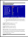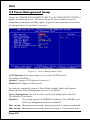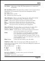
1
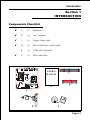
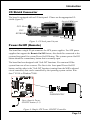
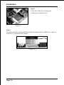
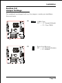
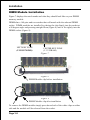
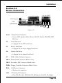
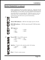
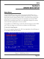
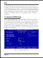
User’s Manual An AMD Soc ket A Pr ocessor based Sock Processor mainboard (100MHz) Suppor ts PC133/V C133 Memor y Modules Supports PC133/VC133 Memory TRADEMARK All products and company names are trademarks or registered trademarks of their respective holders. These specifications are subject to change without notice. 60002KM10 Manual Revision 1.0 October 3, 2000 Table of Contents Section 1 Introduction Page Components Checklist ........................................ 1-1 Overview AMD DuronTM & AthlonTM Processors ............. 1-2 Accelerated Graphics Port .................................. 1-3 Hardware Monitoring .......................................... 1-3 Mainboard Form-Factor ...................................... 1-4 I/O Shield Connector .......................................... 1-5 Power-On/Off (Remote) ..................................... 1-5 System Block Diagram ........................................ 1-6 Section 2 Features Mainboard Features ............................................. 2-1 Section 3 Installation Mainboard Detailed Layout ................................. 3-2 Easy Installation Procedure CPU Insertion ...................................................... 3-3 Jumper Settings ................................................... 3-5 System Memory Configuration .......................... 3-7 Device Connectors .............................................. 3-9 Section 4 Award BIOS Setup Main Menu ........................................................... 4-1 Standard CMOS Setup ......................................... 4-2 Advanced BIOS Features ..................................... 4-3 Advanced Chipset Features ................................. 4-8 Integrated Peripherals ......................................... 4-12 Power Management Setup ................................... 4-16 PNP/PCI Configuration ...................................... 4-19 PC Health Status .................................................. 4-21 Frequency/Voltage Control ................................. 4-22 Defaults Menu ..................................................... 4-23 Supervisor/User Password Setting ..................... 4-24 Exit Selecting ...................................................... 4-25 Appendix Appendix A Load Setup Defaults ............................................ A-1 Appendix B GHOST 5.1 Quick Users Guide ......................... B-1 Introduction Section 1 INTRODUCTION Components Checklist 9 A. (1) Mainboard 9 B. (1) Users manual 9 C. (1) Floppy ribbon cable 9 D. (1) ATA-66 Hard drive ribbon cable E. (1) USB Cable (Optional) F. (1) Driver and utility 9 USERS MANUAL C D B A E or F Page 1-1 Introduction Overview AMD DuronTM & AthlonTM Processors The AMD AthlonTM is a seventh-generation micro architecture with an integrated L2 cache, which is powerful enough to support the bandwidth requirements of a large range of applications, hardware, graphics, and memory technologies. These processors implement advanced design techniques such as: Socket A (PGA 462) 200MHz system interface based on the Alpha EV6 bus protocol. Three out-of-order, superscalar, pipelined Multimedia Units. Three out-of-order, superscaler, pipelined Integer Units. Fixed-sized internal instruction formats (MacroOPs). 72-entry Instruction Control Units. AMD enhanced 3DNow! technology L1 and L2 caches. Dynamic branch prediction. Socket A is the name for AMDs new socketed interface designed to support both AMD DuronTM and AMD AthlonTM processors. This innovation is made possible by integrating the L2 cache memory on chip with the processor. Socket A will help enable smaller enclosures, and ultimately result in a wider variety of solutions in the market. The AMD DuronTM & AthlonTM processors in the Socket A format continue to deliver the ultimate performance for cutting-edge applications. Both bring to desktop systems running industry-standard x86 software superscalar RISC performance. Being provided in the Socket A format they are the worlds most powerful x86 processors. They easily deliver the highest integer, floating-point, and 3D multimedia performance for applications running on x86 platforms around. Page 1-2 Introduction The AMD DuronTM processor is derived from the AMD AthlonTM processor core. It features full-speed, on-chip cache memory, a 200MHz front side system bus, and enhanced 3DNow! technology. Although both processors are related, there are key differences. The AMD AthlonTM processor is targeted at the performance segment, and as such will have more cache memory and higher clock speeds. Accelerated Graphics Port (AGP or A.G.P.) Typically, 3D graphics rendering requires a tremendous amount of memory, and demands ever increasing throughput speed as well. As 3D products for the personal computer become more and more popular, these demands will only increase. This will cause a rise in costs for both end users and manufacturers. Lowering these costs as well as improving performance is the primary motivation behind AGP. By providing a massive increase in the bandwidth available between the video card and the processor, it will assist in relieving some of these pressures for quite sometime. Hardware Monitoring Hardware monitoring allows you to monitor various aspects of your systems operations and status. The features include CPU temperature, voltage and RPM of fan. Page 1-3 Introduction Mainboard Form-Factor The board is designed with Micro ATX form factor - the new industry standard of chassis. Micro ATX form factor is essentially a Baby-AT baseboard rotated 90 degrees within the chassis enclosure and a new mounting configuration for the power supply. With these changes the processor is relocated away from the expansion slots, allowing them all to hold full length add-in cards. Micro ATX defines a double height aperture to the rear of the chassis which can be used to host a wide range of onboard I/O. Only the size and position of this aperture is defined, allowing PC manufacturers to add new I/O features (e.g.; TV input, TV output, joystick, modem, LAN, etc.) to systems. This will help systems integrators differentiate their products in the marketplace, and better meet your needs. Smaller size promotes a smaller system size. I/O shield does not need to be retooled in an Micro ATX 2.01 or later. The mainboard should be used in an Micro ATX 2.01 (or later) compliant case. A smaller power supply can be used. High integration on mainboard reduces the system costs. Expandable I/O Single chassis fan for system ATX Power Supply ATX power connector CPU located near Power Supply Floppy / IDE connectors close to peripheral bays Page 1-4 3 1/2" Bay 5 1/4" Bay Figure 2: Summary of ATX chassis features Introduction I/O Shield Connector The board is equipped with an I/O back panel. Please use the appropriate I/O shield (figure 3). Joystick/Midi port parallel port PS/2 Mouse USB port PS/2 KEYBOARD COM1 COM2 Speaker Line_in MIC Figure 3: I/O back panel layout Power-On/Off (Remote) The board has a single 20-pin connector for ATX power supplies. For ATX power supplies that support the Remote On/Off feature, this should be connected to the systems front panel for system Power On/Off button. The systems power On/Off button should be a momentary button that is normally open. The board has been designed with Soft Off" functions. You can turn Off the system from one of two sources: The first is the front panel Power On/Off button, and the other is the "Soft Off" function (coming from the M/Bs onboard circuit controller) that can be controlled by the operating system such as Windows® 95/98 or Windows®2000. ATX POWER SUPPLY J3 Case (chassis) Power ON/OFF button (J 3) Figure 4: Simple ATX Power ON/OFF Controller Page 1-5 Introduction System Block Diagram AMD Socket A Processors 100MHz 4X 66MHz PAC PCI Bridge and memory controller VT8363 133/100MHz )+ '% VT82C686A I/O Bridge USB 0,1 USB 2,3 Figure 5: System Block Diagram Page 1-6 .A=JKHAI Section 2 FEATURES Mainboard Features: PROCESSOR - AMD Athlon TM, Duron TM Processors, Socket A, operating at 600MHz ~ 1GHz CHIPSET - VIA KT133 AGPset DRAM MODULE - 168pin DIMM x 3 for PC133/VC133 Memory - DRAM Size: 32MB to 1GB EXPANSION SLOT - PCI x 3, 4: AGP x 1 ONBOARD I/O - On-Chip I/O integrated with K/B, Mouse, FDD, Parallel and Serial, Fast IR and Power-ON controllers ONBOARD PCI / IDE - PCI Bus IDE Port with PIO / Ultra DMA-66 x 2 (Up to 4 Devices) I/O CONNECTOR - PS/2 Mouse and PS/2 style Keyboard USB - USB connector x 4 (2 for Opt.) Page 2-1 .A=JKHAI BIOS - Award Plug & Play BIOS Built-in AC97 Digital Audio(by VT82C686A) - Dual full-duplex Direct Sound channels - H/W Sound Blaster Pro for DOS legacy compatibility - FM synthesis for legacy compatibility - Supports game and MIDI port EXTENDED FUNCTION - Supports exclusive USDM(Unified System Diagnostic Manager) and Hardware Monitoring Function by VT82C686A - Supports Wake-On-LAN Function - CPU Clock Setting (1 or 2 increment) via BIOS FORM FACTOR - 245mm x 200mm Micro ATX Size Page 2-2 Installation Section 3 INSTALLATION Page 3-1 Installation Mainboard Detailed Layout Figure 1 Page 3-2 Installation Easy Installation Procedure The following must be completed before powering on your new system: 3-1. 3-2. 3-3. 3-4. CPU Insertion Jumper Settings System memory Configuration Device Connectors Section 3-1 CPU Insertion CPU Insertion: (use AMD AthlonTM as reference) Step 1 Open the socket by raising the actuation lever. Figure 2 Step 2 Insert the processor. Figure 3 Ensure proper pin 1 orientation by aligning the FC-PGA corner marking with the socket corner closest to the actuation arm tip. The pin field is keyed to prevent misoriented insertion. Dont force processor into socket. If it does not go in easily, check for mis-orientation and debris. Make sure the processor is fully inserted into the socket on all sides. Page 3-3 Installation Step 3 Close the socket by lowering and locking the actuation lever. Figure 4 Step 4 Thermal conductive and qualified heatsink recommended by AMD are a must to avoid CPU overheated and burned. Figure 5 Page 3-4 Installation Section 3-2 Jumper Settings The mainboard was designed with very few jumpers to make your installation faster and easier. JP1 JP3 CMOS Clear JP1 = 1-2 Normal (Default) = 2-3 Clear CMOS Power Loss Recovery JP3 = 1-2 Disabled (Default) = 2-3 Enabled Page 3-5 Installation CPU Host Clock Select JP5 JP6 Page 3-6 JP5 JP6 Host Clock 1-2 1-2 100MHz 2-3 2-3 133MHz Installation Section 3-3 System Memory Configuration Memory Layout The board supports (2) PC133/VC133 168-pin DIMMs (Dual In-line Memory Module). The DIMMs is for SDRAM (Synchronous DRAM) only. SDRAM may be 83MHz (12ns), 100MHz (10ns), 125MHz (8ns) or 133MHz (7.5ns) bus speed. If you use both 50ns and 60ns memory you must configure your BIOS to read 60ns. When using Synchronous DRAM we recommend using the 4 clock variety over the 2 clock. Figure 6 and Table 1 show several possible memory configurations. DIMM 1 Bank 0/1 DIMM 2 Bank 2/3 Synchronous DRAM Figure 6 Total Me mory DIMM 1 (Bank 0/1) DIMM 2 (Bank 2/3) = 512MB Maximum SDRAM* 32MB, 64MB, 128MB, 256MB, 512MB X 1 None = 1GB Maximum SDRAM* 32MB, 64MB, 128MB, 256MB, 512MB X 1 SDRAM* 32MB, 64MB, 128MB, 256MB, 512MB X 1 Table 1 * SDRAM supports 32, 64, 128, 256MB, 512MB DIMM modules. * We recommend to use PC100/VC100 Memory Module for bus speed 100MHz and PC133/VC133 Memory for bus speed over 100MHz. * Using non-compliant memory with higher bus speed (over clocking) may severely compromise the integrity of the system. Page 3-7 Installation DIMM Module Installation Figure 7 displays the notch marks and what they should look like on your DIMM memory module. DIMMs have 168-pins and two notches that will match with the onboard DIMM socket. DIMM modules are installed by placing the chip firmly into the socket at a 90 degree angle and pressing straight down (figure 8) until it fits tightly into the DIMM socket (figure 9). LEFT KEY ZONE (UNBUFFERED) CENTER KEY ZONE (3.3 V DRAM) Figure 7 Figure 8 DIMM Module clip before installation Figure 9 DIMM Module clip after installation To remove the DIMM module simply press down both of the white clips on either side and the module will be released from the socket. Page 3-8 Installation Section 3-4 Device Connectors parallel port PS/2 Mouse Joystic/Midi USB port PS/2 KEYBOARD COM1 COM2 Speaker Line_in MIC Figure 10 J2,J3: Chassis Panel Connector Power_LED, Speaker, Reset, Power ON/Off, Turbo LED, HDD LED, IR Conn., J4: CPU Fan Power A plug-in for the CPU Fan Power J5: Power Fan Power A plug-in for the Power Supply Fan Power J6: Chassis Fan Power A plug-in for the chassis Fan Power J7: WOL (Wake On Lan) Connector IDE1: Primary IDE Connector (White Color) IDE2: Secondary IDE Connector (Black Color) FDD1: Floppy Controller Connector (Black Color) PW1: ATX Power Connector 20-pin power connector CD1: CD Audio_IN Connector Pin1(CD_IN_Left), Pin2/Pin3(CD_Reference), Pin4(CD_IN_Right) Page 3-9 Installation AUX1: Auxiliary Line_IN Connector Pin1(Left Line_IN), Pin2/Pin3(GND), Pin4(Right Line-IN) MODEM1: Telephony Connector Pin1(Audio_in), Pin2/Pin3(GND), Pin4(Mic-out to Modem) CN1: Front Panel Audio Connector Line_Out_L $ GND Line_Out_R GND Line_In_L Line_In_R GND MIC_In GND # Note: Either Front Panel Audio or onboard rear audio could be used at one time. USB2: USB port header pins for adding two additional USB ports. VCC $ GND -Data +Data +Data -Data GND VCC # USB port header pin descriptions. PIN# Wire color Signal Name Comment 1 Red Vcc Cable Power 2 White -Data Data 3 Green +Data Data 4 Black Ground Cable Ground 5 Black Ground Case Ground 6 Black Ground Case Ground 7 Black Ground Cable Ground 8 Green +Data Data 9 White -Data Data 10 Red Vcc Cable Power Page 3-10 Installation Device Connectors (continued) (This is connected to the power button on the case. Using the Soft-Off by Pwr-BTTN feature, you can choose either Instant Off (turns system off immediatly), or 4 sec delay (you need to push the button down for 4 seconds before the system turns off). When the system is in 4 sec delay mode, there is a special feature to make the system to go into suspend mode when the button is pressed momentarily). J3 Power On/Off 1 Turbo LED indicator - LED ON when higher speed is selected + IDE LED indicator - LED ON when Onboard PCI IDE Hard disks + is activate IR Connector 1 J2 1. VCC 2. NC 3. IRRX 4. GND 5. IRTX Power LED - Power LED connector 1 1. Power LED(+) 2. N/C 3. GND 4. NC 5. GND Speaker - Connect to the system's speaker for beeping 1 1 1. Speaker 2. N/C 3. GND 4. GND Reset - Closed to restart system. Page 3-11 Installation Page Left Blank Page 3-12 BIOS Section 4 AWARD BIOS SETUP Main Menu Awards ROM BIOS provides a built-in Setup program which allows user to modify the basic system configuration and hardware parameters. The modified data will be stored in a battery-backed CMOS, so that data will be retained even when the power is turned off. In general, the information saved in the CMOS RAM will stay unchanged unless there is a configuration change in the system, such as hard drive replacement or a device is added. It is possible for the CMOS battery to fail, this will cause data loss in the CMOS only. If this does happen you will need to reconfigure your BIOS settings. To enter the Setup Program : Power on the computer and press the <Del> key immediately, this will bring you into the BIOS CMOS SETUP UTILITY. Figure 1: CMOS Setup Utility Page 4-1 BIOS The menu displays all the major selection items. Select the item you need to reconfigure. The selection is made by moving the cursor (press any direction key ) to the item and pressing the Enter key. An on-line help message is displayed at the bottom of the screen as the cursor is moved to various items which provides a better understanding of each function. When a selection is made, the menu of the selected item will appear so that the user can modify associated configuration parameters. 4-1 Standard CMOS Setup Choose Standard CMOS Setup in the CMOS SETUP UTILITY Menu (Figure 2). The Standard CMOS Setup allows the user to configure system settings such as the current date and time, type of hard disk drive installed, floppy drive type, and display type. Memory size is auto-detected by the BIOS and displayed for your reference. When a field is highlighted (use direction keys to move the cursor and the <Enter> key to select), the entries in the field can be changed by pressing the <PgDn> or the <PgUp> key. Figure 2: Standard CMOS Setup Page 4-2 BIOS NOTE: If the hard disk Primary Master/Slave and Secondary Master/ Slave are set to Auto, then the hard disk size and model will be auto-detected. NOTE: The Halt On: field is used to determine when to halt the system by the BIOS if an error occurs. NOTE: Floppy 3 Mode support is a mode used to support a special 3.5 drive used in Japan. This is a 3.5 disk that stores only 1.2 MB, the default setting for this is disabled. 4-2 Advanced BIOS Features Selecting the BIOS FEATURES SETUP option in the CMOS SETUP UTILITY menu allows users to change system related parameters in the displayed menu. This menu shows all of the manufacturers default values for the board. Pressing the [F1] key will display a help message for the selected item. Figure 3: BIOS Features Setup Page 4-3 BIOS Virus Warning: During and after the system boots up, any attempt to write to the boot sector or partition table of the hard disk drive will halt the system and an error message will appear. You should then run an anti-virus program to locate the virus. Keep in mind that this feature protects only the boot sector, not the entire hard drive. The default value is Disabled. Enabled: Activates automatically when the system boots up causing a warning message to appear when anything attempts to access the boot sector. Disabled: No warning message will appear when anything attempts to access the boot sector. Note: Many disk diagnostic programs that access the boot sector table can trigger the virus warning message. If you plan to run such a program, we recommend that you first disable the virus warning. CPU Internal Cache: This controls the status of the processors internal cache area. The default is Enabled. Enabled: This activates the CPUs internal cache thereby increasing performance. Disabled: This deactivates the CPUs internal cache thereby lowering performance. External (L2) Cache: This controls the status of the external (L2) cache area. The default is Enabled. Enabled: This activates the CPUs L2 cache thereby increasing performance. Disabled: This deactivates the CPUs L2 cache thereby lowering performance. CPU L2 Cache ECC Checking: This control if the CPUs L2 Cache will support Error Checking and Correcting (ECC). The default is Disabled. Enabled: Enables ECC support for the CPUs L2 cache. Performance will decrease 2% ~ 4%. Disabled: Disables ECC support for the CPUs L2 cache. Quick Power On Self Test: This category speeds up the Power On Self Test (POST). The default is Enabled. Enabled: This setting will shorten or skip of the items checked during POST. Disabled: Normal POST. Page 4-4 BIOS First /Second/Third/Other Boot Device: The BIOS attempts to load the operating system from the devices in the sequence selected in these items. The choice: Floppy, LS120, HDD, SCSI, CDROM, Disabled. Swap Floppy Drive: This will swap your physical drive letters A & B if you are using two floppy disks. The default is Disabled. Enabled: Floppy A & B will be swapped under the O/S. Disabled: Floppy A & B will be not swapped. Boot Up Floppy Seek: During Power-On-Self-Test (POST), BIOS will determine if the floppy disk drive installed is 40 or 80 tracks. Only 360K type is 40 tracks while 760K, 1.2MB and 1.44MB are all 80 tracks. The default is Enabled. Enabled: The BIOS will search the floppy disk drive to determine if it is 40 or 80 tracks. Disabled: The BIOS will not search for the type of floppy disk drive by track number. Note: BIOS can not tell the difference between 720K, 1.2MB and 1.44MB drive types as they are all 80 tracks. Boot Up NumLock Status: This controls the state of the NumLock key when the system boots. The default is On. On: The keypad acts as a 10-key pad. Off: The keypad acts like the cursor keys. Gate A20 Option: This refers to the way the system addresses memory above 1MB (extended memory). The default is Normal. Normal: The A20 signal is controlled by the keyboard controller or chipset hardware. Fast: The A20 signal is controlled by Port 92 or chipset specific method. Typematic Rate Setting: This determines the keystrokes repeat rate. The default is Disabled. Enabled: Allows typematic rate and typematic delay programming. Disabled: The typematic rate and typematic delay will be controlled by the keyboard controller in your system. Page 4-5 BIOS Typematic Rate (Chars/Sec): This is the number of characters that will be repeated by a keyboard press. The default is 6. 6: 6 characters per second. 8: 8 characters per second. 10: 10 characters per second. 12: 12 characters per second. 15: 15 characters per second. 20: 20 characters per second. 24: 24 characters per second. 30: 30 characters per second. Typematic Delay (msec): This setting controls the time between the first and the second character displayed by typematic auto-repeat. The default is 250. 250: 250 msec. 500: 500 msec. 750: 750 msec. 1000: 1000 msec. Security Option: This category allows you to limit access to the System and Setup, or just to Setup. The default is Setup. System: The system will not boot and the access to Setup will be denied if the correct password is not entered at the prompt. Setup: The system will boot; but the access to Setup will be denied if the incorrect password is not entered at the prompt. OS Select For DRAM > 64MB: Some operating systems require special handling. Use this option only if your system has greater than 64MB of memory. The default is Non-OS2. OS2: Select this if you are running the OS/2 operating system with greater than 64MB of RAM. Non-OS2: Select this for all other operating systems and configurations. Video BIOS Shadow: This option allows video BIOS to be copied into RAM. Video Shadowing will increase the video performance of your system. The default is Enabled. Enabled: Video shadow is enabled. Disabled: Video shadow is disabled. C8000 - CBFFF Shadow: CC000 - CFFFF Shadow: D0000 - D3FFF Shadow: D4000 - D7FFF Shadow: Page 4-6 BIOS D8000 - DBFFF Shadow: DC000 - DFFFF Shadow: These categories determine whether ROMs from option cards will be copied into RAM. This will be in 16K byte or 32K byte units, and the size will depend on chipset of the option card. Enabled: Optional shadow is enabled. Disabled: Optional shadow is disabled. Page 4-7 BIOS 4-3 Advanced Chipset Features Choose the CHIPSET FEATURES SETUP in the CMOS SETUP UTILITY menu to display following menu. Figure 4: Chipset Features Setup DRAM Timing By SPD: Select Enabled for setting SDRAM timing by SPD. The Choice: Enabled, Disabled. DRAM Clock : The item will synchronize/asynchronize DRAM operation clock. Host Clock: DRAM has same working clock with CPU host bus. 2/3 Host: DRAM running with lower operation clock. SDRAM Cycle length: This setting defines the CAS timing parameter of the SDRAM in terms of clocks. The default is 3. 2: Provides faster memory performance. 3: Provides better memory compatibility. Auto: Determined by BIOS. Bank Interleave: The item allows you to set how many banks of SDRAM support in your mainboard. The Choice: 2 Bank, Disabled. Page 4-8 BIOS DRAM Page-Mode: The item will active or inactive chipset page registers. Enabled: Page-Mode Enabled. Disabled: No page registers update and non Page-Mode operation. Memory Hole : You can reserve this memory area for the use of ISA adaptor ROMs. The default is Disabled. Enabled: This field enables the main memory (15~16MB) to remap to ISA BUS. Disabled: Normal Setting. Note: If this feature is enabled you will not be able to cache this memory segment. P2C/C2P Concurrency: This item allows you to enable/disable the PCI to CPU, CPU to PCI concurrency. Fast R-W Turn Around: This item controls the DRAM timing. It allows you to enable/disable the fast read/write turn around. System BIOS Cacheable: This allows you to copy your BIOS code from slow ROM to fast RAM. The default is Disabled. Enabled: The option will improve system performance. However, if any program writes to this memory area, a system error may result. Disabled: System BIOS non-cacheable. Video BIOS Cacheable: This option copies the video ROM BIOS to fast RAM (C0000h to C7FFFh). The default is Enabled. Enabled: Enables the Video BIOS Cacheable to speed up the VGA Performance. Disabled: Will not use the Video BIOS Cacheable function. Video RAM Cacheable: This option allows the CPU to cache read/writes of the video RAM. The default is Enabled. Enabled: This option allows for faster video access. Disabled: Reduced video performance. AGP Aperture Size: The amount of system memory that the AGP card is allowed to share. The default is 64. 4: 4MB of systems memory accessable by the AGP card. 8: 8MB of systems memory accessable by the AGP card. Page 4-9 BIOS 16: 16MB of systems memory accessable by the AGP card. 32: 32MB of systems memory accessable by the AGP card. 64: 64MB of systems memory accessable by the AGP card. 128: 128MB of systems memory accessable by the AGP card 256: 256MB of systems memory accessable by the AGP card. AGP-4X Mode: Chipset AGP Mode support. Options: x1 , x2 and x4. AGP Driving Control: This item allows you to adjust the AGP driving force. Choose Manual to key in a AGP Driving Value in the next selection. This field is recommended to set in Auto for avoiding any error in your system. AGP Fast Write: Selecting Enabled allows to use Fast Write Protocol for 4X AGP. Default is recommended. K7 CLK_CTL Select: Use this item to specify the clock control for ramp rate. Select default for a defaulted time value, and optimal for optimum time value which depends on different CPU ratio. The choice: Default, Optimal OnChip USB/USB2: USB Connector (Port 0-1)/(Port 2-3). The choice: Enabled, Disabled. USB Keyboard/Mouse Support: This controls the activation status of an optional USB keyboard/Mouse that may be attached. The default is disabled. Enabled: Enable USB keyboard/Mouse support. Disabled: Disable USB keyboard/Mouse support. OnChip Sound: Turn on/off onchip sound device. CPU to PCI Write Buffer: When enabled, up to four D words of data can be written to the PCI bus without interruting the CPU. When disabled, a write buffer is not used and the CPU read cycle will not be completed until the PCI bus signals that it is ready to receive the data. The Choice: Enabled, Disabled. Page 4-10 BIOS PCI Dynamic Bursting: When Enabled, data transfers on the PCI bus, where possible, make use of the high-performance PCI bust protocol, in which graeater amounts of data are transferred at a single command. The Choice: Enabled, Disabled. PCI Master 0 WS Write: When Enabled, writes to the PCI bus are command with zero wait states. The Choice: Enabled, Disabled. PCI Delay Transaction: The chipset has an embedded 32-bit posted write buffer to support delay transactions cycles. Select Enabled to support compliance with PCI specification version 2.1. The Choice: Enabled, Disabled. PCI #2 Access #1 Retry: This item allows you enabled/disable the PCI #2 Access #1 Retry. The Choice: Enabled, Disabled. AGP Master 1 WS Write: When Enabled, writes to the AGP (Accelerated Graphics Port) are executed with one wait states. The Choice: Enabled, Disabled. AGP Master 1 WS Read: When Enabled, read to the AGP (Accelerated Graphics Port) are executed with one wait states. The Choice: Enabled, Disabled. Page 4-11 BIOS 4-4 Integrated Peripherals Figure 5: Integrated Peripherals Note: If you do not use the Onboard IDE connector, then you will need to set Onboard Primary PCI IDE: Disabled and Onboard Secondary PCI IDE: Disabled Note: The Onboard PCI IDE cable should be equal to or less than 18 inches (45 cm.). OnChip IDE Channel0: The default value is Enabled. Enabled: Enables Onboard IDE primary port. Disabled: Disables Onboard IDE primary port. OnChip IDE Channel1: The default is Enabled. Enabled: Enables Onboard IDE secondary port. Disabled: Disables Onboard IDE secondary port. IDE Prefetch Mode: Enable prefetching for IDE drive interfaces that support its faster drive accesses. If you are getting disk drive errors, change the setting to omit the drive interface where the errors occur. Depending on the configuration of your IDE subsystem, this field may not appear, and it does not appear when the Internal PCI/IDE field, above, is Disabled. The Choice: Enabled, Disabled. Page 4-12 BIOS Primary Master PIO: The default is Auto. Auto: BIOS will automatically detect the Onboard Primary Master PCI IDE HDD Accessing mode. Mode 0~4: Manually set the IDE Programmed interrupt mode. Primary Slave PIO: The default is Auto. Auto: BIOS will automatically detect the Onboard Primary Slave PCI IDE HDD Accessing mode. Mode 0~4: Manually set the IDE Programmed interrupt mode. Secondary Master PIO: The default is Auto. Auto: BIOS will automatically detect the Onboard Secondary Master PCI IDE HDD Accessing mode. Mode 0~4: Manually set the IDE Programmed interrupt mode. Secondary Slave PIO: The default is Auto. Auto: BIOS will automatically detect the Onboard Secondary Slave PCI IDE HDD Accessing mode. Mode 0~4: Manually set the IDE Programmed interrupt mode. Primary Master UDMA: This allows you to select the mode of operation for the hard drive. The default is Auto. Auto: The computer will select the optimal setting. Disabled: The hard drive will run in normal mode. Primary Slave UDMA: This allows you to select the mode of operation for the hard drive. The default is Auto. Auto: The computer will select the optimal setting. Disabled: The hard drive will run in normal mode. Secondary Master UDMA: This allows you to select the mode of operation for the hard drive. The default is Auto. Auto: The computer will select the optimal setting. Disabled: The hard drive will run in normal mode. Secondary Slave UDMA: This allows you to select the mode of operation for the hard drive. The default is Auto. Auto: The computer will select the optimal setting. Disabled: The hard drive will run in normal mode. Page 4-13 BIOS Init Display First: If two video cards are used (1 AGP and 1 PCI) this specifies which one will be the primary display adapter. The default is PCI Slot. PCI Slots: PCI video card will be primary adapter. AGP: AGP video card will be primary adapter. IDE HDD Block Mode: IDE Block Mode allows the controller to access blocks of sectors rather than a single sector at a time. The default is Enabled. Enabled: Enabled IDE HDD Block Mode. Provides higher HDD transfer rates. Disabled: Disable IDE HDD Block Mode. Onboard FDD Controller: This controls the state of the onboard floppy controller. The default value is Enabled. Enabled: Enable the Onboard VIA686A Chipss floppy drive interface controller. Disabled: Disable the Onboard VIA686A Chips floppy drive interface controller. Onboard Serial Port 1: This field allows the user to configure the 1st serial port. The default is Auto. AUTO: Enable Onboard Serial port 1 and address is Auto adjusted. COM1: Enable Onboard Serial port 1 and address is 3F8H/IRQ4. COM2: Enable Onboard Serial port 1 and address is 2F8H/IRQ3. COM3: Enable Onboard Serial port 1 and address is 3E8H/IRQ4. COM4: Enable Onboard Serial port 1 and address is 2E8H/IRQ3. Disabled: Disable Onboard SMC CHIPs Serial port 1. Onboard Serial Port 2: This field allows the user to configure the 2nd serial port. The default is Auto. AUTO: Enable Onboard Serial port 2 and address is Auto adjusted. COM1: Enable Onboard Serial port 2 and address is 3F8H/IRQ4. COM2: Enable Onboard Serial port 2 and address is 2F8H/IRQ3. COM3: Enable Onboard Serial port 2 and address is 3E8H/IRQ4. COM4: Enable Onboard Serial port 2 and address is 2E8H/IRQ3. Disabled: Disable Onboard SMC CHIPs Serial port 2. UART 2 Mode: This item allows you to determine which Infra Red (IR) function of onboard I/O chip. The Choice: Standard, ASKIR, HPSIR. Page 4-14 BIOS Onboard Parallel port: This field allows the user to configure the LPT port. The default is 378H / IRQ7. 378H: Enable Onboard LPT port and address is 378H and IRQ7. 278H: Enable Onboard LPT port and address is 278H and IRQ5. 3BCH: Enable Onboard LPT port and address is 3BCH and IRQ7. Disabled: Disable Onboard Winbond Chips LPT port. Onboard Parallel Port Mode: This field allows the user to select the parallel port mode. The default is Normal. Normal: Standard mode. IBM PC/AT Compatible bidirectional parallel port. EPP: Enhanced Parallel Port mode. ECP: Extended Capabilities Port mode. EPP+ECP: ECP Mode & EPP Mode. ECP Mode USE DMA: This field allows the user to select DMA1 or DMA3 for the ECP mode. The default is DMA3. DMA1: This field selects the routing of DMA1 for the ECP mode. DMA3: This field selects the routing of DMA3 for the ECP mode. Parallel Port EPP Type: This item allows you to determine the IR transfer mode of onboard I/O chip. The Choice: EPP1.9, EPP1.7. Onboard Legacy Audio: Legacy Audio enabled/disabled. Sound Blaster: Sound Blaster compatible device enabled/disabled. SB I/O Base Address: Sound Blaster I/O resource selection. SB IRQ Select: Legacy audio device IRQ selection. SB DMA Select: Sound Blaster DMA channel selection. MPU-401: MPU-401 function enabled/disabled. MPU-401 I/O Address: Built-in MPU-401 compatible MIDI I/O port selection: 300-303H 310-313H 320-323H 330-333H (default) Game Port (200-207H): Built-in joystick port support disabled/enabled(default). Page 4-15 BIOS 4-5 Power Management Setup Choose the POWER MANAGEMENT SETUP in the CMOS SETUP UTILITY to display the following screen. This menu allows the user to modify the power management parameters and IRQ signals. In general, these parameters should not be changed unless its absolutely necessary. Figure 6: Power Management Setup ACPI Function: This option allows you to select ACPI Function. The default is Enabled. Enabled: Support ACPI function for new O.S Disabled: No Support ACPI function. You can only change the content of Doze Mode, Standby Mode, and Suspend Mode when the Power Management is set to User Define. Power Management: Use this to select your Power Management selection. The default is User define. Disabled: The system operates in NORMAL conditions (Non-GREEN), and the Power Management function is disabled. Max. saving: Maximum power savings. Inactivity period is 1 minute in each mode. Min. saving: Minimum power savings. Inactivity period is 1 hour in each mode. Page 4-16 BIOS User define: Allows user to define PM Timers parameters to control power saving mode. PM controlled by APM: This option shows weather or not you want the Power Management to be controlled the Advanced Power Management (APM). The default is Yes. Yes: APM controls your PM No: APM does not control your PM Video Off Option: Tells you what time frame that the video will be disabled under current power management settings. The default is Standby. Standby: Video powers off after time shown in standby mode setting. Doze: Video powers off after time shown in doze mode setting. Suspend: Video powers off after time shown in suspend mode setting. N/A: Video power off not controlled by power management. Video Off Method: This option allows you to select how the video will be disabled by the power management. The default is V/H Sync + Blank V/H Sync + Blank: System turns off vertical and horizontal synchronization ports and writes blanks to the video buffer. DPMS: Select this option if your monitor supports the Display Power Management Signaling (DPMS) standard of the Video Electronics Standards Association (VESA). Use the software supplied for your video subsystem to select video power management values. Blank Screen: System only writes blanks to the video buffer. MODEM Use IRQ: Name the interrupt request (IRQ) line assigned to the modem (if any) on your system. Activity of the selected IRQ always awakens the system. Default is IRQ 3. N/A: No IRQ is used. 3: IRQ 3 4: IRQ 4 5: IRQ 5 7: IRQ 7 9: IRQ 9 10: IRQ 10 11: IRQ 11 Soft-Off by PWRBTN: Use this to select your soft-off function. The default is Delay 4 sec. Instant Off: Turns off the system instantly. Page 4-17 BIOS Delay 4 Second : Turns off the system after a 4 second delay. If momentary press of button, the system will go into Suspend Mode. Press the power botton again to take system out of Suspend Mode. State After Power Failure: This field lets you determine the state that your PC returns to after a power failure. If set to Off, the PC will not boot after a power failure, if set to On, the PC will restart after a power failure. VGA: When set to On (default), any event occurring at a VGA port will awaken a system which has been powered down. LPT & COM: When set to On (default), any event occurring at a COM(serial)/ LPT (printer) port will awaken a system which has been powered down. HDD & FDD: When set to On (default), any event occurring at a hard or floppy drive port will awaken a system which has been powered down. PCI Card: When set to On (default), any event occurring to the DMA controller will awaken a system which has been powered down. Modem Ring Resume: When set to Enabled, any event occurring to the Modem Ring will awaken a system which has been powered down. RTC Alarm Resume: When set to Enable rtc alarm resume, you could set the date (of month) and timer (hh:mm:ss), any event occurring at will awaken a system which has been powered down. Primary INTR: When set to On (default), any event occurring at will awaken a system which has been powered down. Page 4-18 BIOS 4-6 PNP/PCI Configuration The PNP/PCI configuration program is for the user to modify the PCI/ISA IRQ signals when various PCI/ISA cards are inserted in the PCI or ISA slots. WARNING: Conflicting IRQs may cause the system to not find certain devices. Figure 7: PCI Configuration Setup PNP OS Installed: Do you have a PNP OS installed on your system. The default is No. Yes: Select if you are using a PNP OS. No: Select if your OS does not support PNP. Resources Controlled By: Who controlled the system PNP/PCI resources. The default is Auto. Manual: PNP Cards resources will be controlled manually. You can set which IRQ-X and DMA-X are assigned to PCI/ISA PNP or Legacy ISA Cards. Auto: If your ISA card and PCI card are all PNP cards, BIOS will assign the interrupt resource automatically. Page 4-19 BIOS Reset Configuration Data: This setting allows you to clear ESCD data. The default is Disabled Disabled: Normal Setting. Enabled: If you have plugged in some Legacy cards to the system and they were recorded into ESCD (Extended System Configuration Data), you can set this field to Enabled in order to clear ESCD. PCI/VGA Palette Snoop: Leave this field at Disabled. The choice: Enabled, Disabled. Assign IRQ For VGA/USB: This item allows BIOS to assign whether IRQ is with VGA/USB or not. If you have not connect the VGA/USB device. Can release the IRQ for other device. The default is Enabled. Enabled: Provides IRQ for VGA/USB device. Disabled: Release IRQ for other device. PCI Latency Timer (CLK): The latency timer defines the minimum amount of time, in PCI clock cycles, that the bus master can retain the ownership of the bus. The Choice: 0-255. INT Pin 1 to Pin 4 Assignment : These settings allow the user to specify what IRQ will be assigned to PCI devices in the chosen slot. Options available: Auto,3, 4,5,7,9,10,11,12,14 & 15. The defaults are Auto. Page 4-20 BIOS 4-7 PC Health Status 31oC/87oF 0oC/32oF 6135 RPM 0 RPM 1.62V 1.52V 3.22V 5.01V 12.12V Current CPU Temperature: This is the current temperature of the CPU. Current System Temperature: This is the Current temperature of the system. Current CPU FAN Speed: The current CPU fan speed in RPMs. Current Chassis FAN Speed: The current chassis fan speed in RPMs. CPU(V): The voltage level of the CPU(Vcore). AGP Vcore: The voltage level of Power supplied to AGP card. 1.52V: for 4X AGP card. 3.3V : for 2X AGP card. 3.3V, 5V, 12V: The voltage level of the switch power supply. Page 4-21 BIOS 4-8 Frequency/Voltage Control Auto Detect DIMM/PCI Clk: When enabled the motherboard will automatically disable the clock source for a DIMM socket which does not have a module in it. Same applies for PCI slots. The default is Enabled. Enabled: Enables this option. Disabled: Disables this option. CPU Host/PCI/Spread Spec. : Allows the external clock to be modified depending upon what FSB has been selected. Should not be used to clock processor faster than it was designed for. The default is Default. Page 4-22 BIOS 4-9 Defaults Menu Selecting Defaults from the main menu shows you two options which are described below Load Fail-Safe Defaults When you press <Enter> on this item you get a confirmation dialog box with a message similar to: Load Fail-Safe Defaults (Y/N) ? N Pressing Y loads the BIOS default values for the most stable, minimal-performance system operations. Load Optimized Defaults When you press <Enter> on this item you get a confirmation dialog box with a message similar to: Load Optimized Defaults (Y/N) ? N Pressing Y loads the default values that are factory settings for optimal performance system operations. Page 4-23 BIOS 4-10 Supervisor/User Password Setting You can set either supervisor or user password, or both of then. The differences between are: supervisor password : can enter and change the options of the setup menus. user password : just can only enter but do not have the right to change the options of the setup menus. When you select this function, the following message will appear at the center of the screen to assist you in creating a password. ENTER PASSWORD: Type the password, up to eight characters in length, and press <Enter>. The password typed now will clear any previously entered password from CMOS memory. You will be asked to confirm the password. Type the password again and press <Enter>. You may also press <Esc> to abort the selection and not enter a password. To disable a password, just press <Enter> when you are prompted to enter the password. A message will confirm the password will be disabled. Once the password is disabled, the system will boot and you can enter Setup freely. PASSWORD DISABLED. When a password has been enabled, you will be prompted to enter it every time you try to enter Setup. This prevents an unauthorized person from changing any part of your system configuration. Additionally, when a password is enabled, you can also require the BIOS to request a password every time your system is rebooted. This would prevent unauthorized use of your computer. You determine when the password is required within the BIOS Features Setup Menu and its Security option. If the Security option is set to System, the password will be required both at boot and at entry to Setup. If set to Setup, prompting only occurs when trying to enter Setup. Page 4-24 BIOS 4-11 Exit Selecting Save & Exit Setup Pressing <Enter> on this item asks for confirmation: Save to CMOS and EXIT (Y/N)? ; Pressing Y stores the selections made in the menus in CMOS a special section of memory that stays on after you turn your system off. The next time you boot your computer, the BIOS configures your system according to the Setup selections stored in CMOS. After saving the values the system is restarted again. Exit Without Saving Pressing <Enter> on this item asks for confirmation: Quit without saving (Y/N)? ; This allows you to exit Setup without storing in CMOS any change. The previous selections remain in effect. This exits the Setup utility and restarts your computer. Page 4-25 BIOS Page Left Blank Page 4-26 Appendix Appendix A NOTE: The "LOAD Optimized DEFAULTS" function loads the system default data directly from ROM and initializes the associated hardware properly. This function will be necessary when you accept this mainboard, or the system CMOS data is corrupted. CMOS Setup Utility - Copyright ( C ) 1984-1998 Standard CMOS Feature Frequency/Voltage Control Advanced BIOS Feature Load Fail-Safe Defaults Advanced Chipset Feature Load Optimized Defaults Integrated Peripherals Set Supervisor Password Set User Password Power Management Setup Load Optimized Defaults (Y/N)? Y Save & Exit Setup PnP/PCI Configurations Exit Without Saving PC Health Status ↑ ↓ ← → : Select Item Esc : Quit F10 : Save & Exit Setup Time, Date, Hard Disk Type . LOAD Optimized DEFAULTS A-1 Appendix Page Left Blank A-2 User Notice No part of this product, including the product and software may be reproduced, transmitted, transcribed, stored in a retrieval system, or translated into any language in any form without the express written permission of EPoX Computer Company (hereinafter referred to as EPoX) except for documentation kept by the purchaser for backup purposes. We provide this manual as is without warranty of any kind, either expressed or implied, including but not limited to the implied warranties or conditions of merchantability or fitness for a particular purpose. In no event shall EPoX be liable for any loss of profits, loss of business, loss of use or data, interruption of business or for indirect, special incidental, or consequential damages of any kind, even if EPoX has been advised of the possibility of such damages arising from any defect or error in the manual or product. EPoX may revise this manual from time to time without notice. For updated BIOS, drivers, or product release information you may visit our websites at http://www.epox.com or http://www.epox.com.tw. Products mentioned in this manual are mentioned for identification purposes only. Product names appearing in this manual may or may not be registered trademarks or copyrights of their respective companies. The product name and revision number are both printed on the mainboard itself. Handling Procedures Static electricity can severely damage your equipment. Handle the KT-133M and any other device in your system with extreme care and avoid unnecessary contact with system components on the mainboard. Always work on an antistatic surface to avoid possible damage to the mainboard from static discharge. Always have the power supply unplugged and powered off when inserting and removing devices within the computer chassis. EPoX assumes no responsibility for any damage to the KT-133M mainboard that results from failure to follow instruction or failure to observe safety precautions. CAUTION The KT-133M mainboard is subject to damage by static electricity. Always observe the handling procedures. Technical Support Services If you need additional information, help during installation or normal use of this product, please contact your retailer. Your retailer will have the most current information about your configuration. If your retailer cannot help, you may visit our online technical support website and/or contact our support technicians at the locations listed below. Record your serial number before installing your KT-133M mainboard. (The serial number is located near the ISA slots at the edge of the board.) KT-133M serial number: ____________________________ Contacting Technical Support EPoX technical support is working hard to answer all of your questions online. From our website you can find answers to many common questions, drivers, BIOS updates, tech notes, and important technical bulletins. If you are still unable to locate the solution you are seeking, you always have the option to contact our support technicians directly. North American website (English language) http://www.epox.com [email protected] [email protected] European website (Multi-language) http://www.epox.nl [email protected] [email protected] [email protected] Taiwan website (Chinese language) http://www.epox.com.tw [email protected] [email protected] Thank you for using EPoX mainboards! Copyright 2000 EPoX Computer Company. All rights reserved.