1
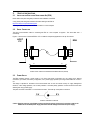
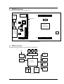
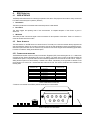
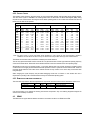
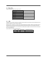
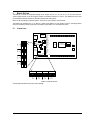
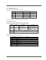
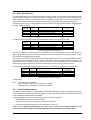
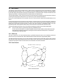
EDK2612
USER MANUAL
FOR H8S/2612
ON-CHIP FLASH MICROCONTROLLER
Preface
Cautions
1.
This document may be, wholly or partially, subject to change without notice.
2.
All rights reserved. No one is permitted to reproduce or duplicate, in any form, a part or this entire
document without Hitachi Micro Systems Europe Limited's written permission.
Trademarks
General
All brand or product names used in this manual are trademarks or registered trademarks of their respective
companies or organisations.
Specific
Microsoft, MS and MS-DOS are registered trademarks and Windows and Windows NT are
trademarks of Microsoft Corporation.
Document Information
Product Code:
D003560_11
Version:
1.0
Date:
09/04/2002
Copyright © Hitachi Semiconductor America 2000-2002. All rights reserved.
Copyright © Hitachi Micro Systems Europe Ltd. 1995-2002. All rights reserved.
Copyright © Hitachi Europe Ltd. 1995-2002. All rights reserved.
Global:
http://www.hitachisemiconductor.com
USA:
http://semiconductor.hitachi.com
Europe:
http://www.hitachi-eu.com/semiconductors
http://www.hmse.com
2
1.
TABLE OF CONTENTS
1.
TABLE OF CONTENTS ............................................................................................................................................. 3
2.
START-UP INSTRUCTIONS ....................................................................................................................................... 4
2.1. INSTALLING THE EVALUATION DEVELOPMENT KIT (EDK)........................................................................... 4
2.2. SERIAL CONNECTION ....................................................................................................................................... 4
2.3. POWER SUPPLY ................................................................................................................................................ 4
3.
EDK BOARD LAYOUT ............................................................................................................................................ 5
3.1. EDK BLOCK DIAGRAM....................................................................................................................................... 5
4.
EDK OPERATION ................................................................................................................................................... 6
4.1. USER INTERFACE.............................................................................................................................................. 6
4.2. SERIAL INTERFACE........................................................................................................................................... 6
4.3. SRAM................................................................................................................................................................... 7
4.4. MEMORY MAP .................................................................................................................................................... 8
4.5. LEDS.................................................................................................................................................................... 8
5.
BOARD OPTIONS .................................................................................................................................................... 9
5.1. JUMPER LINKS................................................................................................................................................... 9
5.2. USER MODE SETTINGS – CJ5........................................................................................................................ 10
5.3. EDK OPTIONS – CJ4 ........................................................................................................................................ 10
5.4. SERIAL PORT SELECTION.............................................................................................................................. 11
5.5. FLASH PROGRAMMING HEADER .................................................................................................................. 11
5.6. BOOT CONTROL .............................................................................................................................................. 12
6.
CODE DEVELOPMENT ........................................................................................................................................... 13
6.1. ADDITIONAL INFORMATION ........................................................................................................................... 13
3
2.
START-UP INSTRUCTIONS
2.1. INSTALLING THE EVALUATION DEVELOPMENT KIT (EDK)
Please refer to the quick start guide provided for initial installation of the EDK.
A copy of the quick start guide and other information relating to this EDK at:
http://www.hmse.com/products/edk/support/
Installing the EDK requires power and serial connection to a host computer.
2.2. SERIAL CONNECTION
The serial communications cable for connecting the EDK to a host computer is supplied. The serial cable has 1:1
connectivity.
Figure 2-1 shows how to connect the EDK to a PC or notebook computer equipped with a nine pin D connector.
HOST
PC
EDK
3
2
5
3
2
5
FIGURE 2-1: SERIAL CONNECTION TO PC/NOTEBOOK WITH DB-9 CONNECTOR (SUPPLIED)
2.3. POWER SUPPLY
The EDK hardware requires a power supply of +5V. Since total power consumption can vary widely due to external
connections, port states, and memory configuration, use a power supply capable of providing at least 500mA at +5V DC ±
5%.
The design is specified for evaluation of the microcontroller and so does not include circuitry for supply filtering/noise
reduction, under voltage protection, over current protection or reversed polarity protection. Caution should be used when
selecting and using a power supply.
The power connector on the EDK is a 2.5mm Barrel connector. The center pin is the positive connection.
FIGURE 2-2: POWER SUPPLY CONNECTION
Caution: Existing customers using E6000 products note that the polarity of this board is opposite to that for the
E6000. Use of the E6000 power supply with this board will damage both board and power supply.
4
3.
EDK BOARD LAYOUT
The diagram shows a general layout of the EDK board.
FLASH
Programming
Power
BOOT LED
Power LED
User1 LED
User2 LED
9-W ay
D-Type
J1
5V
3V3
UVcc
GND
Testpoints
XTAL
RESn
FW
NMIn
ULED1
ULED2
PSCK
PTXD
PRXD
RX232
DTXD
DRXD
NMI
Switch
RESET
Switch
MD4
BOOT
Switch
HITACHI
Microprocessor
MD4
MD4
MD4
CJ5
MD4
MD4
MD4
MD4
MD4
HCAN
MD4
J2
CJ4
FIGURE 3-1: EDK BOARD LAYOUT
3.1. EDK BLOCK DIAGRAM
The diagram shows the connectivity of the components on the EDK board.
5V PSU
Reset
Boot
NMI
Switches
EDK specific
Control Logic
5V Supply
&
3V3 Regulator
RS232
Programming
& Comms
SRAM
HCAN Driver
HITACHI
Microprocessor
Display
Module
LEDs
User1 Power
&
&
User2 Boot
Header
Connectors
On-Chip
Debug
Connector
FIGURE 3-2: EDK BLOCK DIAGRAM
5
4.
EDK OPERATION
4.1. USER INTERFACE
The EDK provides three buttons for influencing the operation of the board. The purpose of each button is clearly marked next
to it. Refer to the board layout for positions (Section 3)
1.
Reset Switch
This button provides the microcontroller with a timed reset pulse of at least 250mS.
2.
Boot Switch
This button toggles the operating mode of the microcontroller. A complete description of this function is given in
section 5.6.
3.
NMI Switch
This button provides a de-bounced signal to the microcontroller for each operation of the button. There is no minimum or
maximum activation time for this button.
4.2. SERIAL INTERFACE
The serial interface on the EDK board has several functions. The serial port on the microcontroller directly supports three
wire serial interfaces. Options are provided on the board for the user to write handshaking routines using standard port pins.
Other board option links allow users to control the entry and exit from boot mode using the same handshaking signals. Refer
to section 5 for details on setting serial interface options.
4.2.1. CONNECTOR PIN DEFINITIONS
The EDK RS232 interface conforms to Data Communication Equipment (DCE) format allowing the use of 1-1 cables when
connected to Data Terminal Equipment (DTE) such as an IBM PC. The cable used to connect to the EDK will affect the
available board options. A fully wired cable can allow handshaking between the microcontroller and the host PC, subject to
setting the board options and the availability of suitable host software. Handshaking is not supported as standard on the
microcontroller so for normal use a minimal three-wire cable can be used. The minimum connections are unshaded in the
following table.
EDK DB9
Connector Pin
1
2
3
4
5
6
7
8
9
Signal
Host DB9
Connector Pin
No Connection
EDK Tx Host Rx
EDK Rx Host Tx
No Connection
Ground
No Connection
* EDK CTS Host RTS
* EDK RTS Host CTS
No Connection
1
2
3
4
5
6
7
8
9
TABLE 4-1: RS232 INTERFACE CONNECTIONS
* These are not connected on the EDK by default. See section 5.4 for more details.
5
4
9
3
8
2
7
1
6
FIGURE 4-1: EDK SERIAL PORT PIN NUMBERING
6
4.2.2. CRYSTAL CHOICE
The operating crystal frequency has been chosen to support the fastest operation with the fastest serial operating speeds.
The value of the crystal is 18.432MHz. The following table shows the baud rates and Baud Rate Register (BRR) setting
required for each communication rate using the above default operating speed. It also confirms the resultant baud rate and
the bit error rate that can be expected.
Baud Rate Register Settings for Serial Communication Rates
SMR
Setting:
Comm.
Baud
110
0
BRR
setting
Actual
Rate
1
ERR
(%)
BRR
setting
Actual
Rate
2
3
ERR
(%)
BRR
setting
Actual
Rate
ERR
(%)
BRR
setting
Actual
Rate
ERR
(%)
-0.22
Invalid
Invalid
Invalid
Invalid
Invalid
Invalid
Invalid
Invalid
Invalid
81
110
300
Invalid
Invalid
Invalid
Invalid
Invalid
Invalid
119
300
0.00
29
300
0.00
1200
Invalid
Invalid
Invalid
119
1200
0.00
29
1200
0.00
7
1125
-6.25
2400
239
2400
0.00
59
2400
0.00
14
2400
0.00
3
2250
-6.25
4800
119
4800
0.00
29
4800
0.00
7
4500
-6.25
1
4500
-6.25
9600
59
9600
0.00
14
9600
0.00
3
9000
-6.25
Invalid
Invalid
Invalid
19200
29
19200
0.00
7
18000
-6.25
1
18000
-6.25
Invalid
Invalid
Invalid
38400
14
38400
0.00
3
36000
-6.25
Invalid
Invalid
Invalid
Invalid
Invalid
Invalid
Invalid
57600
9
57600
0.00
2
48000
-16.67
Invalid
invalid
Invalid
Invalid
Invalid
115200
4
115200
0.00
0
144000
25.00
Invalid
Invalid
Invalid
Invalid
Invalid
Invalid
230400*
2
192000
-16.67
Invalid
Invalid
Invalid
Invalid
Invalid
Invalid
Invalid
Invalid
Invalid
460800*
0
576000
25.00
Invalid
Invalid
Invalid
Invalid
Invalid
Invalid
Invalid
Invalid
Invalid
TABLE 4-2 CRYSTAL FREQUENCIES FOR RS232 COMMUNICATION
* Note: The device used to convert the RS232 serial information to logic signals for the microcontroller is limited to
120kBaud. The rates above this level can only be utilised if the user provides direct logic level communications.
The default communication rate for the EDK is indicated by the shaded selection.
The user may replace the HC49/U surface mounted AT cut crystal with another of similar type within the operating frequency
of the microcontroller device. Please refer to the hardware manual for the microcontroller for the valid operating range.
Alternatively the user may fit an oscillator module – or provide an external clock source. When providing an oscillator module
or external source it is highly recommended that the load capacitors for the AT crystal are removed from the PCB. These are
physically placed within the PCB outline of the oscillator module for easy location and to ensure they are removed when
using this option.
When changing the crystal frequency the pre-loaded debugging monitor will not function. In this situation the user is
responsible for providing code to evaluate the device away from the default operating speed.
4.2.3. REMOVABLE COMPONENT INFORMATION.
This information is provided to allow the replacement of components removed from the board as described in section 4.2.2.
Component
Load Resistor
Load capacitors
Cct. Ref
R8
C6,C7
Value
1MΩ
12pF
Rating
0805 1%
0603 10% 25V
Manufacturer
Welwyn WCR Series
AVX 0603 3 A 150 KAT
TABLE 4-3: REMOVABLE COMPONENT INFORMATION
Care must be taken not to damage the tracking around these components. Only use soldering equipment designed for
surface mount assembly and rework.
4.3. SRAM
This EDK does not support external address and data bus connections so there is no SRAM on this EDK.
7
4.4. MEMORY MAP
Table 4-4 illustrates the EDK memory map for mode 7.
Section End
Section Start
Section Allocation
H’00000000
H’01FFFF
H’FFE000
H’FFEFBF
H’FFF800
H’FFFF3F
H’FFFF60
H’FFFFBF
H’FFFFC0
H’FFFFFF
Oh-Chip ROM
On-chip RAM
Internal I/O registers
Internal I/O registers
On Chip RAM
TABLE 4-4: MEMORY MAP (DEFAULT MODE 2)
4.5. LEDS
The EDK has four red LEDs. The function of each LED is clearly marked on the silk screen of the PCB. Please refer to the
board layout diagram for position information (Section 3).
When the board is connected to a power source the Power (PWR) led will illuminate. The Boot mode indication LED will
illuminate when the microcontroller has been placed into Boot mode. Please see section 0 for more details of this function.
There are two LEDs dedicated for user control these are marked USR1 and USR2. Each LED will illuminate when the port
pin is in a logical high state.
The user LEDs are connected to the following ports:
LED
Identifier
USR1
USR2
Port
Pin
P15
P16
Microcontroller
Pin
3
4
Pin Functions on Port Pin
P15/PO13/TIOCB1/TCLKC
P16/PO14/TIOCA2/nIRQ1
TABLE 4-5: LED PORT CONNECTIONS
8
5.
BOARD OPTIONS
The EDK has a number of configuration settings set by jumpers CJ4 (A, B, C, D) CJ5 (A, B, C, D) and zero-ohm links.
Common EDK functions can be set using the jumpers as described in sections 5.3 and 5.2. The additional zero-ohm links
provide additional features that may be required to interface with other systems.
All the Jumper link settings are three pin options. There are four sets of options on each header.
The headers are numbered from 1 to 12 with pin 1 marked on the PCB by an arrow pointing to the pin. The diagram below
shows the numbering of these jumper links and indicates jumpers fitted 1-2 for each three-pin jumper.
5.1. JUMPER LINKS
MD4
FLASH
Programming
5V
3V3
UVcc
GND
Power
RESn
FW
NMIn
ULED1
ULED2
PSCK
PTXD
PRXD
RX232
DTXD
DRXD
NMI
Switch
1
1 2 3
Jumper
B
1,2,3
4
1 2 3
Jumper
C
1,2,3
7
2
1 2
3
Jumper
A
1,2,3
BOOT LED
Power LED
User1 LED
User2 LED
RESET
Switch
BOOT
Switch
XTAL
SRAM
HITACHI
Microprocessor
OSC
HCAN
3
MD4
MD4
MD4
HCAN
CJ5
5
9-Way
D-Type
J1
MD4
MD4
MD4
MD4
MD4
6
MD4
J2
8
CJ4
9 10 11
12
1 2 3
Jumper
D
1,2,3
1 2
3
1 2 3
Jumper
A
1,2,3
4
5
6
1 2 3
Jumper
B
1,2,3
7
8
9 10 11
1 2 3
Jumper
C
1,2,3
12
1 2 3
Jumper
D
1,2,3
FIGURE 5-1: JUMPER CONFIGURATION
The following tables define each jumper and its settings.
9
5.2. USER MODE SETTINGS – CJ5
CJ5 is used to set the operating mode of the microcontroller.
These jumpers must be fitted at all times to ensure correct operation of the EDK.
Jumper
CJ 5-A
Default 2-3
CJ 5-B
Default 1-2
CJ 5-C
Default 2-3
CJ 5-D
Default 1-2
Function
Setting 1-2
Setting 2-3
User Mode Setting Bit 0
MD0 pulled High
MD0 pulled Low
User Mode Setting Bit 1
MD1 pulled High
MD1 pulled Low
User Mode Setting Bit 2
MD2 pulled High
MD2 pulled Low
User Mode Setting Bit 3
MD3 pulled High
MD3 pulled Low
TABLE 5-1: USER MODE: JUMPER SETTINGS (DEFAULT SETTINGS IN BOLD)
The default settings indicated in bold text place the microcontroller into Mode 7.
5.3.
EDK OPTIONS – CJ4
The EDK options provide access to commonly used features of the EDK range.
These jumpers must be fitted at all times to ensure correct operation of the EDK.
Jumper
Function
CJ 4-A
Default 2-3
Serial Receive
Source
CJ 4-B
Default 2-3
User
Programming
Mode
Setting 1-2
Disables the RS232 receive signal
to enable the use of the Flash
Programming Header
Disables the Flash write hardware
protection.
The flash can be overwritten in
User Mode.
CJ 4-C
Setting 2-3
Enables the RS232 receive signal.
The Flash Programming Header*
must not be used in this state.
Enables the Flash write hardware
protection.
The flash can not be overwritten in
User Mode.
No Function
Default No Fit
CJ 4-D
No Function
Default No Fit
TABLE 5-2: BOARD OPTION: JUMPER SETTINGS (DEFAULT SETTINGS IN BOLD)
*See section 5.5
The following table lists the connections to each jumper pin.
Pin
1
2
3
4
5
6
7
8
9
10
11
12
Net Name
UVCC
RXDISn
No Connection
UVCC
UPM
No Connection
No Connection
No Connection
No Connection
No Connection
No Connection
No Connection
Description
Microcontroller Supply Voltage
Disable Flash Header functions. Pulled low. (Enables RX232)
No Connection
Microcontroller Supply Voltage
CPLD Controlled option to set Flash Write (FW). Pulled low.
No Connection
No Connection
No Connection
No Connection
No Connection
No Connection
No Connection
10
5.4. SERIAL PORT SELECTION
The programming serial port is connected to the RS232 connector by default. This allows direct programming of the EDK
using the supplied software tools. A secondary serial port is available on the microcontroller and can be connected to the
RS232 connector by changing some board option links. The additional port option allows the user to write messages or
connect to other devices via the serial port while programming support is provided by the Flash programming header.
The following surface mount, zero-ohm link settings are fitted by default and connect the RS232 header to the programming
serial port of the microcontroller.
Zero-ohm
Link ID
CR20
CR23
CR19
CR22
Default
Fitted
Fitted
Not Fitted
Not Fitted
Function
Transmit data from EDK
Receive data to EDK
Alternate Transmit data from EDK
Alternate Receive data to EDK
Microcontroller
Port Pin
PA1
PA2
PC0
PC1
TABLE 5-3: OPTION LINKS – DEFAULT SETTINGS
To enable the use of this alternate port the user must change the settings to those in the following table.
Zero-ohm
Link ID
CR20
CR23
CR19
CR22
Default
Not Fitted
Not Fitted
Fitted
Fitted
Function
Transmit data from EDK
Receive data to EDK
Alternate Transmit data from EDK
Alternate Receive data to EDK
Microcontroller
Port Pin
PA1
PA2
PC0
PC1
TABLE 5-4: OPTION LINKS – ALTERNATE SERIAL PORT
The user may implement a handshaking protocol on the EDK. This is not supported with the software tools supplied. To
support this option two spare port pins have been allocated on the microcontroller. Using these port pins the CTS and RTS
lines of the host serial interface can be controlled.
The user may also control the operation of the board via the same handshaking lines. This is not supported with the software
tools supplied but may be written by the user. Using the CTS line the user may simulate pressing the boot button, see
section:5.6. This will cause the EDK to swap into and out of Boot mode on each low-level activation of CTS. Feedback of the
current mode is provided on the RTS line. A high level indicates boot mode and a low level indicates user mode.
The following settings are made by default, and ensure that there are no conflicts on unnecessary microcontroller pins.
Zero-ohm
Link ID
CR12
CR7
CR16
CR13
Default
Not Fitted
Not Fitted
Not Fitted
Not Fitted
Function
Mode State out from EDK
Change Mode request to EDK
Alternate RTS232 – Ready to send – from EDK
Alternate CTS232 – Clear to send – to EDK
Microcontroller
Port Pin
N/A (From CPLD*)
N/A (From CPLD*)
PF4
PF0
TABLE 5-5: OPTION LINKS – SERIAL PORT CONTROL
* See section 5.6
Note:
These setting pairs are exclusive:
If CR12 and CR7 are fitted; CR16 and CR13 must not be fitted.
If CR16 and CR13 are fitted; CR12 and CR7 must not be fitted.
5.5. FLASH PROGRAMMING HEADER
The Flash Programming header is used with the Hitachi Flash Debug Board (FDB). The FDB is a USB based programming
tool for control and programming of Hitachi microcontrollers, available separately from Hitachi. This header provides direct
access for the FDB to control the EDK microcontroller.
To utilise this header the user must make the following changes to the board configuration.
1.
Disable the RX232 signal from the RS232 transceiver.
Jumper link CJ4-A is provided for this purpose. Please refer to section 5.3.
2.
Disable User Program Mode using jumper CJ4-B. Please refer to section 5.3.
Caution: Do not operate the board with the user mode jumpers removed and the FDB disconnected as the
microcontroller mode pins will float to an indeterminate state. This may damage the microcontroller device.
11
5.6. BOOT CONTROL
The method for placing the microcontroller device in to Boot mode for reprogramming has been incorporated into a complex
programmable logic device (CPLD). This is not necessary for most user designs but allows a measure of increased flexibility
for the EDK designs. Mode transitions including boot mode transitions only require the reset to be held active while the mode
settings are presented. On releasing reset the microcontroller will be in the required mode.
The logic design detects a power up event and provides a timed reset pulse to guarantee the reset of the device. At the end
of the rest pulse the processor will be placed in user mode and any code in the device will execute.
During user mode the NMI button can be pressed at any time. This will provide a single de-bounced NMI interrupt to the
device.
Pressing the boot button will cause the boot mode controller to reset the device and, during the reset period, present the
required mode settings to start the device in boot mode. At the end of the reset period the boot mode settings will have been
latched into the device which will then be ready to accept a boot mode connection via the RS232 interface or the flash
programming header. Pressing the boot button during a normal reset will not cause the EDK to enter boot mode.
The boot mode settings are fixed at mode 3. The required mode settings are made using a tri-state capable buffer.
Note:
The boot control device is programmed to support all possible EDK products.
For this reason the reset pulse is over 500ms. Repetitive activation of either the Boot or Reset buttons will restart
the reset timer and extend the reset period. Pressing the boot button within the 500mS period of a reset will not
cause the board to enter boot mode.
5.6.1. CPLD CODE
The code is based upon a four state machine providing a guaranteed reset period which can be extended by holding the
relevant control input in the active state. When released the timer will extend the reset for approximately 500mS.
The states are split into two functions, one for User mode and one for Boot mode. The first state of each is used to hold the
reset line active. When the timer expires then the second state is used to hold the device in the selected mode and wait for
an external control signal to either move back into the user reset state or into the boot reset state.
5.6.2. STATE DIAGRAM
Boot Mode Controller : Positive Logic
(CTS+BootSw) . /Res
Waiting
Boot
/Res . Boot
Res
Reset Timer
/Res
ResSw . /Res
Res
/Res
/Res . Reset
Clocked Transitions
using NE555
(All solid transition
lines)
Reset
(BootSW + ResSw + CTS)
. /Res
BootWaiting
Async
FIGURE 5-2: CPLD STATE DIAGRAM
12
6.
CODE DEVELOPMENT
6.1. ADDITIONAL INFORMATION
For details on how to use Hitachi Embedded Workshop (HEW), with HDI-m, the EDK’s resident debugger, refer to the HEW
manual available on the CD or from the web site.
For information about the H8S series microcontrollers refer to the H8S Series Hardware Manual
For information about the H8S assembly language, refer to the H8S Series Programming Manual
Further information available for this product can be found on the HMSE web site at:
http://www.hmse.com/products/edk/support/edk2612.htm
General information on Hitachi Microcontrollers can be found at the following URLs.
Global:
http://www.hitachisemiconductor.com
USA:
http://semiconductor.hitachi.com
Europe:
http://www.hitachi-eu.com/semiconductors
http://www.hmse.com
13