1
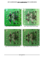
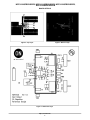
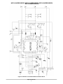
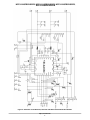
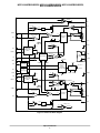
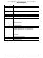
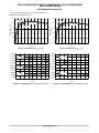
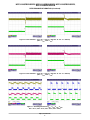
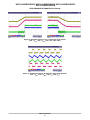
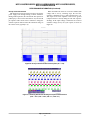
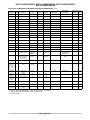
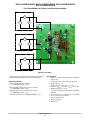
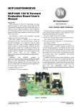
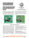
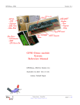
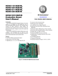
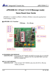
NCP3120QPBCKGEVB, NCP3121QPBCKGEVB, NCP3122QPBCKGEVB, NCP3123QPBCKGEVB NCP3120-23 2A/3A HF BuckEvaluation Board User'sManual http://onsemi.com EVAL BOARD USER’S MANUAL Circuit Description 750/2,200 kHz. Also, an onboard operational transconductance amplifier (OTA) integrates the error signal to provide high DC accuracy. The NCP312x also includes an enable and disable function with externally controlled soft start and stop. The NCP312x operates as a voltage-mode, pulse-widthmodulated, (PWM) asynchronous buck converter. Its operating frequency is adjustable with an external resistor to ground from 220 kHz to 750/2,200 kHz. minimum switching frequency of 220 kHz and a maximum Table 1. EVALUATION BOARD SPECIFICATION Characteristic Min Input Voltage Output Voltage Output Current Typ Max Unit Comments (Note 1) 7 − 15 V Vout1 − 3.3 − V Vout2 − 5 − V Vout1 0 − 2 A Vout2 0 − 2 A − 300 − kHz − − V EN Tied to SEQ EN Tied to SEQ Oscillator Frequency Enable Threshold High EN Tied to SEQ 2.0 Sequence Threshold Low EN Tied to SEQ − − 0.8 V Voltage Ripple Vout1 − 40 − mVpk−pk Vout2 − 40 − mVpk−pk Load Regulation Vout1 − 0.61 − mV/A (Vin = 12 V, Iout = 0.5 − 2 A) Vout2 − 0.21 − mV/A Line Regulation Vout1 − 1.85 − mV/V (Vin = 10.8 − 13.2 V, Iout = 2 A) Vout2 − 3.53 − mV/V − 160 − C Thermal Shutdown Dual 2 A/3 A DC−DC Converter Dimensions 1 2 Outlined Area 1. Operation down to 4.5 V requires selecting a lower voltage for Vout2. Semiconductor Components Industries, LLC, 2012 November, 2012 − Rev. 1 1 Publication Order Number: EVBUM2159/D NCP3120QPBCKGEVB, NCP3121QPBCKGEVB, NCP3122QPBCKGEVB, NCP3123QPBCKGEVB Figure 1. NCP3120 2 A Buck Evaluation Board Figure 2. NCP3121 3A Buck Evaluation Board Figure 3. NCP3122 2A HF Buck Evaluation Board Figure 4. NCP3123 3A HF Buck Evaluation Board http://onsemi.com 2 NCP3120QPBCKGEVB, NCP3121QPBCKGEVB, NCP3122QPBCKGEVB, NCP3123QPBCKGEVB BOARD DETAILS Figure 5. Top Layer Figure 6. Bottom Layer Figure 7. Silkscreen Layer http://onsemi.com 3 NCP3120QPBCKGEVB, NCP3121QPBCKGEVB, NCP3122QPBCKGEVB, NCP3123QPBCKGEVB Figure 8. Schematic for the NCP3120 Buck Evaluation Board http://onsemi.com 4 NCP3120QPBCKGEVB, NCP3121QPBCKGEVB, NCP3122QPBCKGEVB, NCP3123QPBCKGEVB Figure 9. Schematic for the NCP3121, NCP3122 and NCP3123 Buck Evaluation Boards http://onsemi.com 5 NCP3120QPBCKGEVB, NCP3121QPBCKGEVB, NCP3122QPBCKGEVB, NCP3123QPBCKGEVB 0 .1. ref Falling comp SHDN 1 PG 1 0 .9 . ref pg 1 HS protection 1 COMP 1 Error Amplifier FB 1 VIN Delay R PWM EOTA 1 HS1 CON TR OL LOGIC 1 0o S SW 1 1V GND 1 10 u SS 1 TRACK 1 SS 1 Soft Start & Tracking Control (MUX1) OSCILLATOR RT AVIN FB1 10 u Signal Voltage 0. 5V Overload Protection ref (0.8 V) AGND SHDN 1 SEQ1 EN 1 EN 2 SHDN 1 Power Sequencing 1 TRACK 2 AVIN STAR TU P UVL O TH ER MAL SH U TD OWN Power Sequencing 2 Reference 0. 8V ref (0 .8V ) ref (0.8 V) GND 2 SHDN1 SHDN2 1V SEQ 2 SS2 SHDN2 SHDN 2 10u SS 2 Soft Start & Tracking Control (MUX2) HS protection 2 FB2 10u VIN 0 .5V Overload Protection 180o COMP 2 S Error Amplifier PWM EOTA 2 R HS 2 CON TR OL LOGIC 2 FB 2 SW 2 pg 2 0 .9 . ref PG 2 Delay 0 .1. ref Figure 10. NCP 3120 Block Diagram http://onsemi.com 6 Falling comp SHDN 2 NCP3120QPBCKGEVB, NCP3121QPBCKGEVB, NCP3122QPBCKGEVB, NCP3123QPBCKGEVB Table 2. PIN DESCRIPTION Pin Symbol 1, 31, 32 SW1 2−7 VIN 8–10 SW2 Description Switch node of Channel 1. Connect an inductor between SW1 and the regulator output. Input power supply voltage pins. These pins should be connected together to the input signal supply voltage pin. Switch node of Channel 2. Connect an inductor between SW2 and the regulator output. 11 GND2 12 SS2 Power ground for Channel 2 13 COMP2 14 AGND 15 FB2 Feedback Pin. Used to set the output voltage of Channel 2 with a resistive divider from the output. 16 RT Resistor select for the oscillator frequency. Connect a resistor from the RT pin to AGND to set the frequency of the master oscillator. 17 TRACK 2 Tracking input for Channel 2. This pin allows the user to control the rise time of the second output. This pin must be tied high in the normal operation (except in the tracking mode). 18 TRACK 1 Tracking input for Channel 1. This pin allows the user to control the rise time of the first output. This pin must be tied high in the normal operation (except in the tracking mode). 19 SEQ2 20 EN2 21 SEQ1 Soft-start control input for Channel 2. An internal current source charges an external capacitor connected to this pin to set the soft-start time. Compensation pin of Channel 2. This is the output of the error amplifier and inverting input of the PWM comparator. Analog ground; connect to GND1 and GND2. Sequence pin for Channel 2. I/O used in power sequencing. Connect SEQ to EN for normal operation of a standalone device. Enable input for Channel 2. Sequence pin for Channel 1. I/O used in power sequencing. Connect SEQ to EN for normal operation of a standalone device. 22 EN1 Enable input for Channel 1. 23 PG2 Power good, open-drain output of Channel 2. Output logic is pulled to ground when the output is less than 90% of the desired output voltage. Tied to an external pull-up resistor. 24 PG1 Power good, open-drain output of Channel 1. Output logic is pulled to ground when the output is less than 90% of the desired output voltage. Tied to an external pull-up resistor. 25 AVIN Input signal supply voltage pin. 26 FB1 Feedback Pin. Used to set the output voltage of Channel 1 with a resistive divider from the output. 27 AGND 28 COMP1 29 SS1 30 GND1 Exposed Pad (GND) Analog ground. Connect to GND1 and GND2. Compensation pin of Channel 1. This is the output of the error amplifier and inverting input of the PWM comparator. Soft-start/stop control input for Channel 1. An internal current source charges an external capacitor connected to this pin to set the soft-start time. Power ground for Channel 1. The exposed pad at the bottom of the package is the electrical ground connection of the NCP312x. This node must be tied to ground. http://onsemi.com 7 NCP3120QPBCKGEVB, NCP3121QPBCKGEVB, NCP3122QPBCKGEVB, NCP3123QPBCKGEVB PERFORMANCE INFORMATION The following Figures show typical performance of the NCP312x in this evaluation board. 90 95 Vin = 10.8 V 90 EFFICIENCY (%) 85 EFFICIENCY (%) Vin = 10.8 V Vin = 13.2 V Vin = 12 V 80 75 70 65 Vin = 12 V 85 80 75 0 0.2 0.4 0.6 0.8 1.0 1.2 1.4 1.6 1.8 70 2.0 0.2 0.4 0.6 0.8 1.0 1.2 1.4 1.6 Iout (A) Figure 11. Efficiency for Vout1 = 3.3 V Figure 12. Efficiency @ Vout2 = 5 V 1.8 2.0 4.998 3.3745 4.997 Vin = 13.2 V 3.3740 Vin = 13.2 V 4.996 3.3735 4.995 3.3725 Vout (V) 3.3730 Vin = 12 V 3.3720 4.994 Vin = 12 V 4.993 4.992 3.3715 3.3710 3.3705 3.3700 0 Iout (A) 3.3750 Vout (V) Vin = 13.2 V 0 0.5 Vin = 10.8 V 4.991 Vin = 10.8 V 4.990 1.0 1.5 2.0 4.989 0 Iout (A) 0.5 1.0 1.5 2.0 Iout (A) Figure 13. Load Regulation vs. Vin for Vout1 = 3.3 V Figure 14. Load Regulation vs. Vin for Vout1 = 3.3 V http://onsemi.com 8 NCP3120QPBCKGEVB, NCP3121QPBCKGEVB, NCP3122QPBCKGEVB, NCP3123QPBCKGEVB PERFORMANCE INFORMATION (Continued) Figure 15. Load Transient − Vout1 (Vin = 12 V, Iout = 200 mA −to− 2 A −to− 200 mA) (CH1 = Vout1, CH4 = Iout1) Figure 16. Load Transient − Vout2 (Vin = 12 V, Iout = 200 mA −to− 2 A −to− 200 mA) (CH1 = Vout2, CH4 = Iout2) Figure 17. Switching Waveforms Vout1, Vout2, VSW1, VSW2 CH1 = Vout1, CH2 = Vout2, CH3 = VSW1, CH4 = VSW2) http://onsemi.com 9 NCP3120QPBCKGEVB, NCP3121QPBCKGEVB, NCP3122QPBCKGEVB, NCP3123QPBCKGEVB PERFORMANCE INFORMATION (Continued) Figure 18. Ratiometric Startup of Vout1/2 with Power Good Outputs (CH1 = Vout1, CH2 = Vout2, CH3 = PG1, CH4 = PG2) Figure 19. Switching Waveforms Showing 1805 Phase Shift Operation (CH1 = VSW1, CH2 = VSW2, CH3 = IL1, CH4 = IL2) http://onsemi.com 10 NCP3120QPBCKGEVB, NCP3121QPBCKGEVB, NCP3122QPBCKGEVB, NCP3123QPBCKGEVB PERFORMANCE INFORMATION (Continued) Hiccup Overload Protection When the NCP312x detects an overload condition (FB voltage falls to 0.5 V), switching stops, the soft start capacitor is discharged to 0.1 V and again charged to 1 V. The output of the error amplifier is also tied to ground (output transistor is closed) during the soft start capacitor discharge. If the output voltage is still below the overload condition voltage (0.5 V), the cycle repeats, as shown in Figure 20. The NCP312x uses hiccup mode protection to protect the power supply from damage during overload conditions. During normal operation, the external soft start capacitor is pulled up by a current source that delivers 10 mA to the SS pin capacitor. This current source continues to charge the soft start capacitor until it reaches the saturation voltage of the current source (typically 4 V). Figure 20. Hiccup Overload Protection Description (VIN = 12 V) Figure 21. Switching Waveforms Showing Hiccup Overload Protection (CH1 = VSW1, CH2 = VSW2, CH3 = IL1, CH4 = IL2) http://onsemi.com 11 NCP3120QPBCKGEVB, NCP3121QPBCKGEVB, NCP3122QPBCKGEVB, NCP3123QPBCKGEVB Table 3. BILL OF MATERIAL FOR THE NCP312x EVALUATION BOARD (Note 2) Designator Qty. Description Value Tolerance Footprint Manufacturer Manufacturer Part Number Substitution Allowed Lead Free RT 1 Resistor 240 kW 1% 1206 VISHAY RCA1206240KFKEA Yes Yes RVIN, R14, R24 1 Resistor 100 W 1% 1206 VISHAY RCA1206100R0FKEA Yes Yes R1 1 Resistor 75 kW 1% 1206 VISHAY RCA1206100KFKEA Yes Yes R5, R22 2 Resistor 47 kW 1% 1206 VISHAY RCA120647K0FKEA Yes Yes R6, R23 2 Resistor 15 kW 1% 1206 VISHAY RCA120615K0FKEA Yes Yes R7, R8 2 Resistor 10 kW 1% 1206 VISHAY RCA120610K0FKEA Yes Yes R12 1 Resistor 68 kW 1% 1206 VISHAY RCA120668K0FKEA Yes Yes R13 1 Resistor 13 kW 1% 1206 VISHAY RCA120613K0FKEA Yes Yes R15, R25 2 Resistor 4k7 1% 1206 VISHAY RCA12064K70FKEA Yes Yes R16 1 Resistor 5k1 1% 1206 VISHAY RCA12065K10FKEA Yes Yes R26 1 Resistor 3k3 1% 1206 VISHAY RCA12063K30FKEA Yes Yes C1, C15, C25 3 Ceramic Capacitor 22 mF 10% 1210 Kemet C1210C226K4PAC Yes Yes C2, C3, C11, C21 4 Ceramic Capacitor 100 mF 10% 1206 Epcos B37872A5104K060 Yes Yes C12, C22 2 Ceramic Capacitor 22 mF 10% 1206 Epcos B37872A5223K060 Yes Yes C14, C24 2 Ceramic Capacitor 220 mF 10% 1206 Epcos B37871K5221J060 Yes Yes L11, L21 2 Inductors 22 mF 20% DO3340P Coilcraft DO3340P−223 No Yes LD1, LD2 2 LED Diode − Green LED 3 mm − 3 mm KingBright L−7104GD Yes Yes D11, D21 2 Low Vf Schottky Rectifier (Note 3) MBRS240/ MBRS340/ MBRS360 − SMB/SMC (Note 4) ON Semiconductor MBRS240LT3G/ MBRS340LT3G/ MBRS360LT3G No Yes IC1 1 Dual 2 A/3 A Switching Regulator (200−750 kHz/ 200−2,200 kHz) NCP312x (Note 2) − QFN32 (55 mm) ON Semiconductor NCP312xMNTXG (Note 2) No Yes JP1, JP2, JP7, JP8 4 3 Pin 3 Pin − 2.54 Harwin M20−9990305 Yes Yes JP3, JP4, JP5, JP6, JP9, JP10, JP11, JP12, JP13, JP14, JP15, JP16 12 RM 2.54 mm, PCB pin’s Jumper − PCB pin’s − 2.54 Harwin M20−9990205 Yes Yes Jumper 8 Jumper, RM 2.54 mm Jumper − 2.54 Harwin M7686−05 Yes Yes R3, R4 (Note 5) 2 Resistor NU 1% 1206 − − Yes Yes C13, C16, C23, C26 (Note 5) 4 Ceramic Capacitor NU 10% 1206 − − Yes Yes Plastic Distance 4 Plastic distance − − L 5 mm − − Yes − Screw 4 M3 Screw − − D 36 mm − − Yes − Connecting Ext. Points 17 Connecting external points − − − − − Yes − 2. 3. 4. 5. x = 0, 1, 2, 3 2 A 40 V − NCP3120 & NCP3122; 3 A 60 V − NCP3121; 3 A 40 V − NCP3123 SMB − NCP3120 & NCP3122; SMC − NCP3121 & NCP3123 Not used positions. http://onsemi.com 12 NCP3120QPBCKGEVB, NCP3121QPBCKGEVB, NCP3122QPBCKGEVB, NCP3123QPBCKGEVB TEST PROCEDURE FOR THE NCP312x EVALUATION BOARD DC Electronic Load + A + V − x − DC Power Supply + A + V − − DC Electronic Load + A + − V − Figure 22. Test Setup Test Procedure The following steps detail the test procedure for all these boards: NCP3120, NCP3121, NCP3122 and NCP3123 1. Make sure, if the red ringed jumpers are placed (Figure 22). 2. Connect the test setup as shown in Figure 22. 3. Disable loads = 0 A. 4. Apply an input voltage, VIN = 12 V DC. 5. Check, if VOUT1 = 5 V DC, VOUT2 = 3.3 V DC. 6. Enable loads up to 2 A/3 A* (*for the NCP3121, NCP3123 Buck Evaluation Boards) 7. Check, if VOUT1 = 5 V DC, VOUT2 = 3.3 V DC. 8. If yes, test passed successfully. 9. Power down the load. 10. Power down VIN. 11. End of test. Required Equipment Current limited DC Power Supply (e.g. AGILENT 6653A) − 1pc DC Volt-Meter able to measure up to 15 V DC (e.g. KEITHLEY 2000) − 3pcs DC Amp-Meter able to measure up to 2 A DC (e.g. KEITHLEY 2000) − 3pcs DC Electronic Load (e.g. AGILENT 6060B) − 2pcs http://onsemi.com 13 NCP3120QPBCKGEVB, NCP3121QPBCKGEVB, NCP3122QPBCKGEVB, NCP3123QPBCKGEVB CONFIGURATION OF JUMPERS JP9: JP10: JP11: JP12: JP13: JP14: JP15: JP16: JP1: Enable/Disable 1-st Channel (pins 2−3 enabling, 1−2 disabling the channel 1) JP2: Enable/Disable 2-nd Channel (pins 2−3 enabling, 1−2 disabling the channel 2) JP3: SEQ1 + EN2 JP4: EN2 + SEQ2 JP5: EN1 + SEQ1 JP6: EN1 + SEQ2 JP7: Tracking 1 ref. level − must connect pins 2−3 for normal operation JP8: Tracking 2 ref. level − must connect pins 2−3 for normal operation, connect 1−2 for Tracking function, see the configuration table Internal Tracking 2 Enable Internal enable 1 of Master voltage Soft start 2 Internal enable 2 of Master voltage Soft start 2 External enable of Master voltage Soft start 1 External enable of Master voltage Soft start 2 Track1 + Track2 Soft start 1 capacitor enable Soft start 2 capacitor enable Table 4. CONFIGURATION OF JUMPERS JP1 JP2 JP3 JP4 JP5 JP6 JP7 JP8 JP9 JP10 JP11 JP12 JP13 JP14 JP15 JP16 − 2−3 2−3 − − − − − − 1−2 1−2 − 2−3 2−3 − − − − − − 1−2 1−2 − 2−3 2−3 − − − − − − 1−2 1−2 1−2 2−3 2−3 − − − − − − 1−2 1−2 − − − − − − 1−2 1−2 1−2 1−2 1−2 − − − 1−2 − 1−2 1−2 − − − 1−2 − Normal Operation − Enable from VIN 2−3 2−3 − 1−2 1−2 Enables are Driven from an External Sources − − − 1−2 1−2 Enable 1 is Driven from VIN, Channel 2 is Disabled 2−3 1−2 − 1−2 1−2 Sequential Sequencing − Enable from VIN 2−3 2−3 1−2 − − Enable 1 is Driven from an External Source, Enable 2 is a SLAVE of Enable 1 − − 1−2 − − 1−2 2−3 2−3 Internal Tracking − CH1 is MASTER, CH2 SLAVE; Enable from VIN 2−3 2−3 − 1−2 1−2 1−2 2−3 1−2 Enable1 is Driven from External Source, Enable2 is Connected with Enable1 − − − 1−2 1−2 1−2 2−3 1−2 1−2 ON Semiconductor and are registered trademarks of Semiconductor Components Industries, LLC (SCILLC). SCILLC owns the rights to a number of patents, trademarks, copyrights, trade secrets, and other intellectual property. A listing of SCILLC’s product/patent coverage may be accessed at www.onsemi.com/site/pdf/Patent−Marking.pdf. SCILLC reserves the right to make changes without further notice to any products herein. SCILLC makes no warranty, representation or guarantee regarding the suitability of its products for any particular purpose, nor does SCILLC assume any liability arising out of the application or use of any product or circuit, and specifically disclaims any and all liability, including without limitation special, consequential or incidental damages. “Typical” parameters which may be provided in SCILLC data sheets and/or specifications can and do vary in different applications and actual performance may vary over time. All operating parameters, including “Typicals” must be validated for each customer application by customer’s technical experts. SCILLC does not convey any license under its patent rights nor the rights of others. SCILLC products are not designed, intended, or authorized for use as components in systems intended for surgical implant into the body, or other applications intended to support or sustain life, or for any other application in which the failure of the SCILLC product could create a situation where personal injury or death may occur. Should Buyer purchase or use SCILLC products for any such unintended or unauthorized application, Buyer shall indemnify and hold SCILLC and its officers, employees, subsidiaries, affiliates, and distributors harmless against all claims, costs, damages, and expenses, and reasonable attorney fees arising out of, directly or indirectly, any claim of personal injury or death associated with such unintended or unauthorized use, even if such claim alleges that SCILLC was negligent regarding the design or manufacture of the part. SCILLC is an Equal Opportunity/Affirmative Action Employer. This literature is subject to all applicable copyright laws and is not for resale in any manner. PUBLICATION ORDERING INFORMATION LITERATURE FULFILLMENT: Literature Distribution Center for ON Semiconductor P.O. Box 5163, Denver, Colorado 80217 USA Phone: 303−675−2175 or 800−344−3860 Toll Free USA/Canada Fax: 303−675−2176 or 800−344−3867 Toll Free USA/Canada Email: [email protected] N. American Technical Support: 800−282−9855 Toll Free USA/Canada Europe, Middle East and Africa Technical Support: Phone: 421 33 790 2910 Japan Customer Focus Center Phone: 81−3−5817−1050 http://onsemi.com 14 ON Semiconductor Website: www.onsemi.com Order Literature: http://www.onsemi.com/orderlit For additional information, please contact your local Sales Representative EVBUM2159/D