1
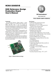
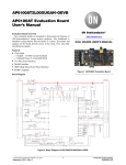
NCN511010GEVB,
NCN512010GEVB,
NCN512110GEVB,
NCN513010GEVB
NCN51XX10GEVB
Evaluation Board
User'sManual
www.onsemi.com
EVAL BOARD USER’S MANUAL
•
•
•
•
Introduction
The NCN51XX10GEVB Evaluation Board is the ideal
solution for developing your KNX application with an
ON Semiconductor KNX transceiver. The evaluation board
contains the KNX transceiver which handles the
transmission and reception of data on the bus. It will also
generate all necessary voltages to power the board and
external loads.
The NCN51XX10GEVB Evaluation Board assures safe
coupling to and decoupling from the KNX bus. Bus
monitoring warns the external microcontroller for loss of
power so that critical data can be stored in time.
•
•
•
•
•
•
•
•
Features
• 9,600 baud KNX Communication Speed
• Supervision of KNX Bus Voltage
• High Efficient 1.2 V to 21 V Selectable DC−DC
Converter to Drive External Loads
Monitoring of Power Regulators
No Additional Power Supply Required
Buffering of Sent Data Frames (Extended Frames
Supported)
Selectable UART or SPI Interface to Host Controller
Selectable UART and SPI Baud Rate to Host Controller
Optional CRC on UART to the Host
Optional MARKER Character to the Host
Optional Direct Coupling of RxD and TxD to Host
(Analog Mode)
Auto Polling (Optional)
Temperature Monitoring
Operating Temperature Range of −40°C to +105°C
Figure 1.The NCN51XX10GEVB Evaluation Board
© Semiconductor Components Industries, LLC, 2015
November, 2015 − Rev. 0
1
Publication Order Number:
EVBUM2338/D
NCN511010GEVB, NCN512010GEVB, NCN512110GEVB, NCN513010GEVB
NCN51XX Description
Table 1. CONNECTOR DESCRIPTION OF THE
NCN51XX10GEVB BOARD
The NCN51XX10GEVB provides an evaluation board
for ON Semiconductor KNX transceivers that can be easily
connected to a prototype design. Table 1 lists the available
connectors on this board.
Connector
Description
J4
KNX Bus Connection
J2
Interface Connector
J1
Interface Connector (alternate)
Electrical Characteristics
Operating ranges define the limits for functional
operation and parametric characteristics of the evaluation
board. Note that the functionality of the evaluation board
outside these operating ranges is not guaranteed. Operating
outside the recommended operating ranges for extended
periods of time may affect device reliability.
Table 2. OPERATING RANGES
Symbol
Parameter
Min
Max
Units
+20
+33
V
VBUS
Voltage on positive pin of J4 (Note 1)
VDIG
Voltage on J1 (Pins 7, 8, 12, 13, 15−22) and J2 (Pins 7, 8, 11, 14−22)
0
+3.3
V
VANA
Output Voltage on J1 (Pin 6) or J2 (Pin 5)
0
+3.3
V
VDD1
Output Voltage on J1 (Pin 24) or J2 (Pin 23)
0
+3.3
V
VDD2
Output Voltage on J1 (Pin 2) or J2 (Pin 1) (Note 2)
0
+21
V
V20V
Output Voltage on J1 (Pin 4) or J2 (Pin 3)
0
+22
V
Ta
Ambient Temperature
−40
+105
°C
1. Voltage indicates DC value. With equalization and active pulse, bus voltage must be between 11 V and 45 V
2. See Adjustable DC*DC Converter page 7 for the limitations!
www.onsemi.com
2
Figure 2.Schematic of NCN51XX10NGEVB
D
C
B
A
Mounting Hole
Mounting Hole
Mounting Hole
Fiducial Round
Fiducial Square
1
C11
100 nF
D4
SS16T3G
D1
C10
1 uF
C12
10 uF
V2
1
2
3
C6 4
5
47 nF
6
7
C8 8
9
220 nF
V20V 10
27 Ohm
100 uF
C9
J5
R5
100 nF
C4
ON Logo (silkscreen, 5,5mm)
R10
39k
R7
120k
Garbage Logo (metal layer, 5,5mm)
Pb−Free Logo (metal layer, 5,5mm)
ESD Logo (silkscreen, 4mm)
2
XTAL1
10 pF
VSSA
VBUS2
TXO
CCP
CAV
VBUS1
CEQ1
CEQ2
VFILT
V20V
U1
10k
0r
3.3V
R4
R3
CE Logo (metal layer, 5mm)
Ground Bar
R1
Fiducial Round
J4
KNX+
KNX−
2 x 13.14.125
243−211
J3
1SMA40CAT3G
16 MHz
C1
X1
As close as possible to U1
C2
10 pF
XTAL2
VDDD
SCK/UC2
SDO/TXD
SDI/RXD
CSB/UC1
TREQ
MODE2
MODE1
TRIG
XCLKC
C13
10 uF
3.3V
NCN5130
30
29
28
27
26
25
24
23
22
21
CSB
TREQ
MODE2 DNP
MODE1
TRIG
XCLKC
SCK
TXD
C3
100 nF
3.3V
C7
2
Next text on top silkscreen: NCN51xx Evaluation Board
Next text on bottom copper layer: NCN51XX_V10_REV2
1 Ohm
R8
1
40
39 ANAOUT
38
37 RESETB
36 SAVEB
35 XTAL1
34 XTAL2
33
32
XCLK
31
VDDA
ANAOUT
FANL
RESET
SAVE
XTAL1
XTAL2
XSEL
XCLK
VSSD
VDD2MV
VDD2MC
VDD2
VSS2
VSW2
VIN
VSW1
VSS1
VDD1
VDD1M
11
12
13
14
15
16
17
18
19
20
3
220 uH
L1
220 uH
L2
1 Ohm
www.onsemi.com
R9
All components (except D1 and D4) as close as possible to U1.
D1 and D4 as close as possible to J4.
R6
DNP
R2
RXD
3.3V
TXD
RXD
CSB
TREQ
MODE2
MODE1
TRIG
XCLKC
XCLK
SCK
ANAOUT
RESETB
SAVEB
V20V
V2
SCK
RXD
TXD
TREQ
CSB
MODE1
MODE2
XCLKC
TRIG
3.3V
XCLK
SAVEB
RESETB
ANAOUT
V20V
V2
613 024 211 21
J1
1
2
3
4
5
6
7
8
9
10
11
12
13
14
15
16
17
18
19
20
21
22
23
24
4
613 024 210 21
J2
1
2
3
4
5
6
7
8
9
10
11
12
13
14
15
16
17
18
19
20
21
22
23
24
C
B
A
D
Variant = Variant name not interpreted
Cannot open
Property of ON Semiconductor, All Rights Reserved
file
C:\Users\ffx3 File:C:\projects\knxb\doc\1_Application\hw\3_Develop\REV10\NCN51xx_Daughterboard.SchDoc
qc\Document Name:Tom De Ryck
Date:27/10/2015
Sheet1 of 1
s\My_Standa Rev: 2
3
4
D3 0 Ohm
NSR0520V2
D2
NSR0520V2
3
NCN511010GEVB, NCN512010GEVB, NCN512110GEVB, NCN513010GEVB
NCN51XX10NGEVB Description
Schematic Diagram − BOM List − PCB Layout
NCN511010GEVB, NCN512010GEVB, NCN512110GEVB, NCN513010GEVB
Table 3. NCN51XX10NGEVB BILL OF MATERIALS
Designator
Qty
Value
(NCN5110)
Description
Value
(NCN5120)
Value
(NCN5121)
C1, C2
2
Multilayer Ceramic, COG, 50 V, ±0, 5 pF, 0402
DNP
C3, C4, C11
3
Multilayer Ceramic, X7R, 10 V, ±10%, 0402
100 nF
C6
1
Multilayer Ceramic, X7R, 50 V, ±10%, 0603
47 nF
Value
(NCN5130)
10 pF
C7
DNP
C8
1
Multilayer Ceramic, X7R, 50 V, ±10%, 0603
220 nF
4.7 nF
220 nF
C9
1
SMD Electrolytic Capacitor, 35 V, ±20%, 8x10
C10
1
Multilayer Ceramic, X7R, 35 V, ±10%, 0603
1 mF
C12, C13
2
Multilayer Ceramic, X7R, 25 V, ±20%, 1206
10 mF
D1
1
1 A Schottky Rectifier, SMA
D4
1
400 Watt SMA Transient Voltage Suppressor,
40 V Bidirectional, SMA
J2
1
WR−PHD Angled Pin Header, Dual Row, 24 Pins,
2,54 mm Pitch
J3
1
EIB (KNX) Bus Coupler Unit Connector, Dark
Grey and Red
J4
1
EIB (KNX) Bus Coupler Unit Pins, 8,5 mm
Length, 5,75 mm pitch
L1, L2
2
WE−PD2SR SMD Shielded Power Inductor,
7,5x8,0
220 mH
R1
1
Shorting Link, Pitch 10.16 mm, Height 9 mm,
Not−Isolated
0r
Thick Film Resistor, 100 mW, ±5%, 0603
0r
100 mF
SS16T3G
D2, D3
DNP
R2
1SMA40CAT3G
Wurth Elektronik 613 024 210 21
Wago 243−211
Ettinger 13.14.125
R3
1
Thick Film Resistor, 100 mW, ±5%, 0603
0r
DNP
0r
R4
1
Thick Film Resistor, 100 mW, ±1%, 0603
10k
DNP
10k
R5
1
Thick Film Resistor, 1 W, ±5%, 2512
27r
22r
27r
R7
1
Thick Film Resistor, 100 mW, ±5%, 0603
120k
33k
120k
R6
DNP
R8, R9
2
Thick Film Resistor, 100 mW, ±1%, 0603
1r
R10
1
Thick Film Resistor, 100 mW, ±5%, 0603
U1
1
ON Semiconductor KNX Transceiver, NQFP−40
X1
1
Crystal, SMD, 4 Pins, 3,2 x 2,5 mm
39k
180k
NCN5110
NCN5120
DNP
www.onsemi.com
4
39k
NCN5121
16 MHz
NCN5130
NCN511010GEVB, NCN512010GEVB, NCN512110GEVB, NCN513010GEVB
Figure 3.Top Layer Layout
Figure 4.Bottom Layer Layout
www.onsemi.com
5
NCN511010GEVB, NCN512010GEVB, NCN512110GEVB, NCN513010GEVB
Figure 5.PCB Dimensions
General Overview
is foreseen (mandatory) as also a Transient Voltage
Suppressor (D2, Figure 2). Minimum VBUS is 20 V (see
KNX standard).
IBUS is limited by the transceiver, as well as the rate of
change of IBUS. This limitation is required by the KNX
standard.
If the FANIN pin is open, IBUS can maximum be 12 mA
and change at 0.5 mA/ms. If the FANIN pin is shorted to
ground, IBUS can maximum be 24 mA and change at
1 mA/ms. For NCN5110 and NCN5130, the FANIN pin can
also have a resistance to ground to set the current limit to any
value between 6mA and 47 mA, with an associated current
slope limitation of 0.23 mA/ms to 1.95 mA/ms.
Because the NCN5120 Development Board contains a
KNX Certified KNX Transceiver no further details on KNX
will be given in this document. Detailed information on the
ON Semiconductor Certified KNX Transceivers can be
found in the NCN5110/NCN5120/NCN5121/NCN5130
datasheets (www.onsemi.com). Detailed information on the
KNX Bus can be found on the KNX website and in the KNX
standards (www.knx.org).
KNX Bus Connection
Connection to the KNX bus is done by means of J4. A
standard Wago connector (type 243*211) can be used for
this (see Figure 6). A reverse protection diode (D1, Figure 2)
Figure 6.KNX Bus Connector
www.onsemi.com
6
NCN511010GEVB, NCN512010GEVB, NCN512110GEVB, NCN513010GEVB
Power Supplies
The DC value of the VFILT line should be higher than
VDD2.
Although VDD2 is capable of delivering 100 mA, the
maximum current capability will not always be usable. One
needs to make sure that the KNX bus power consumption
stays within the KNX specification.
The KNX transceiver provides the power from the bus for
the complete application. The evaluation board will provide
the following voltages to the application.
VFILT
This is an unregulated voltage resulting on a buffer
capacitance, after observing the bus current (slope) limits.
All other voltages are derived from this voltage. If the
application has sharp load transients on any voltage rail,
enough buffer capacitance must be placed on VFILT. See the
datasheet for more information.
Crystal Oscillator
A crystal of 16 MHz (X1, see Figure 11) is foreseen on the
development board. This clock signal is also supplied to the
microcontroller. As the clock signal is only used for digital
services, the NCN5110 does not require a crystal. See the
datasheet (www.onsemi.com) for more details on this block.
V20V:
This is a linear regulated +20 V. Since this voltage is
derived from VFILT, it may be that this voltage is lower than
20 V when the bus voltage is low or when during a load
transient VFILT drops below 20 V. For more information on
this rail and the current limit, see the datasheet.
Interface
The device can communicate with the host controller by
means of a UART interface or an SPI interface. The
selection of the interface and communication speed is done
by the pins MODE1, MODE2, TREQ, SCK/UC2 and
CSB/UC1 which can be pulled up or down, or connected to
the microcontroller. More details on the different interfaces
can be found in the datasheet.
+3V3
A +3V3 is provided from one DCDC convertor. This
voltage is also used as the supply for the transceiver.
Although VDD2 is capable of delivering 100 mA, the
maximum current capability will not always be usable. One
needs to make sure that the KNX bus power consumption
stays within the KNX specification.
Monitoring
RESETB and SAVEB
The KNX transceiver controls the reset state of the
microcontroller by means of the RESETB signal. An
additional SAVEB signal can be monitored by the
microcontroller to detect possible issues. See datasheet for
more details on these two signals.
VDD2
This is a second power supply which can be used to drive
external loads. The voltage is programmable between 1.2 V
(NCN5110/NCN5121/NCN5130) or 3.3 V (NCN5120) and
21 V by means of an external resistor divider (R7 and R10,
see Figure 2).
The voltage divider can be calculated as follows for
NCN5120:
R7 +
R 10 R VDD2M
R 10 ) R VDD2M
Voltage Supervisors
On Semiconductor KNX transceivers have different
voltage supervisors, which can be read out through registers.
Please check the datasheet for more details.
V DD2*3.3
3.3
Temperature Monitor
The transceiver produces an over−temperature warning
(TW) and a thermal shutdown warning (TSD) , which can be
read out through resistors. Please check the datasheet for
more details.
RVDD2M is between 60 k and 140 k (typical 100 k).
The voltage divider can be calculated as follows for
NCN5110/NCN5121/NCN5130:
R 7 + R 10
V DD2*1.2
1.2
www.onsemi.com
7
NCN511010GEVB, NCN512010GEVB, NCN512110GEVB, NCN513010GEVB
FAQ
4. Can we request ON Semiconductor to supply the higher
layer stacks?
By no means will ON Semiconductor provide any higher
layer stacks. Certified higher layer stacks can be provided by
3rd party companies.
5. How much load can the outputs drive?
The maximum allow load can be calculated with the
formula as given in Adjustable DC−DC Converter (page
x13). IDD2 defines the maximum load the outputs can drive
in total.
6. Is it possible to test all interfaces (UART, SPI, Analog
Mode) with this evaluation board?
Yes, the board can be used with all possible interfaces.
One has to be careful however when using the Analog Mode.
In the Analog Mode the digital of NCN5120 is bypassed. If
the microcontroller would force the RXD*pin (pin 29)
high, the transceiver would pull the KNX bus low
continuously, which could lead to issues.
7. I’m having issues with the voltage regulators whenever
I’m going above a certain current. What could be the issue?
To be able to take more than 13 mA from the KNX bus one
needs to pull the FANIN *pin of NCN5120 low. This can
be done by shorting J5 (add jumper). See datasheet for more
info on the FANIN *pin.
Additionally, there is a current limit on V20/3V3/VDD2
1. Is this development board KNX Certified?
No, only the transceiver is KNX Certified. The
development board may only be used for evaluation of the
transceiver. It is not allowed to use the development board
in a final product or to sell it as a KNX Certified product.
Contact ON Semiconductor if you want to use the
development board as a final product.
2. What 3rd party companies do you recommend for the
higher layer stacks?
ON Semiconductor does not recommend any 3rd party
company in particular. Several 3rd party companies have
KNX Certified stacks and it’s always advised to use one of
these stacks. Some companies have experience with ON
Semiconductor KNX transceivers. Contact ON
Semiconductor for more information.
3. Can we freely reuse the schematic and layout of this
development board?
It is allowed to reuse the schematic, components and
layout of the evaluation board for your own application.
Because the operating conditions of your design are not
known by ON Semiconductor, one must always fully verify
the design even if it’s based on this evaluation board. Contact
ON Semiconductor if additional information is required.
ON Semiconductor and the
are registered trademarks of Semiconductor Components Industries, LLC (SCILLC) or its subsidiaries in the United States and/or other countries.
SCILLC owns the rights to a number of patents, trademarks, copyrights, trade secrets, and other intellectual property. A listing of SCILLC’s product/patent coverage may be accessed
at www.onsemi.com/site/pdf/Patent−Marking.pdf. SCILLC reserves the right to make changes without further notice to any products herein. SCILLC makes no warranty, representation
or guarantee regarding the suitability of its products for any particular purpose, nor does SCILLC assume any liability arising out of the application or use of any product or circuit, and
specifically disclaims any and all liability, including without limitation special, consequential or incidental damages. “Typical” parameters which may be provided in SCILLC data sheets
and/or specifications can and do vary in different applications and actual performance may vary over time. All operating parameters, including “Typicals” must be validated for each
customer application by customer’s technical experts. SCILLC does not convey any license under its patent rights nor the rights of others. SCILLC products are not designed, intended,
or authorized for use as components in systems intended for surgical implant into the body, or other applications intended to support or sustain life, or for any other application in which
the failure of the SCILLC product could create a situation where personal injury or death may occur. Should Buyer purchase or use SCILLC products for any such unintended or
unauthorized application, Buyer shall indemnify and hold SCILLC and its officers, employees, subsidiaries, affiliates, and distributors harmless against all claims, costs, damages, and
expenses, and reasonable attorney fees arising out of, directly or indirectly, any claim of personal injury or death associated with such unintended or unauthorized use, even if such claim
alleges that SCILLC was negligent regarding the design or manufacture of the part. SCILLC is an Equal Opportunity/Affirmative Action Employer. This literature is subject to all applicable
copyright laws and is not for resale in any manner.
PUBLICATION ORDERING INFORMATION
LITERATURE FULFILLMENT:
Literature Distribution Center for ON Semiconductor
19521 E. 32nd Pkwy, Aurora, Colorado 80011 USA
Phone: 303−675−2175 or 800−344−3860 Toll Free USA/Canada
Fax: 303−675−2176 or 800−344−3867 Toll Free USA/Canada
Email: [email protected]
N. American Technical Support: 800−282−9855 Toll Free
USA/Canada
Europe, Middle East and Africa Technical Support:
Phone: 421 33 790 2910
Japan Customer Focus Center
Phone: 81−3−5817−1050
www.onsemi.com
8
ON Semiconductor Website: www.onsemi.com
Order Literature: http://www.onsemi.com/orderlit
For additional information, please contact your local
Sales Representative
EVBUM2338/D