1
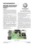
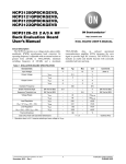
NCP1605FORWGEVB NCP1605 152 W Forward Evaluation Board User's Manual Introduction http://onsemi.com When associated to forward or half−bridge converters taking advantage of a narrow input voltage range, the PFC stage should be designed to start first and to remain active as long as the power supply is plugged in. More specifically, the downstream converter turns on and operates while the output of the PFC stage is nominal. In other words, the PFC must be the master. EVAL BOARD USER’S MANUAL The goal of this user’s manual is to give more information on the practical implementation of this application and to present the performance of the solution. The power supply consists of two stages: • A PFC pre−converter that provides the main converter with a stable 390 Vdc input voltage • The main conversion stage that is a 2−switch forward operating at 133 kHz The 2−switch forward is driven by the NCP1217A. Housed in a SOIC−7 or PDIP−7 package, the NCP1217A eases the design of modern ac−dc adapters and offers a true alternative to UC384X−based designs. This circuit is ideal for 2−switch forward converters. It limits the duty−cycle below 50% and its current mode control topology provides an excellent input audio susceptibility and inherent pulse−by−pulse control. In addition, when the current set point falls below a given value; e.g., when the output power demand diminishes, the IC automatically enters the so−called skip cycle mode and provides high efficiency at light loads. Because this occurs at a user adjustable low peak current, no acoustic noise takes place. For more information, please refer to http://www.onsemi.com/PowerSolutions/product.do?id=N CP1217A. The NCP1605 is a Power Factor Controller especially designed to meet these requirements. This driver features a “pfcOK” pin to enable the downstream converter when the PFC stage is ready for operation. Practically, it is in high state when the output voltage of the PFC stage is within regulation and low otherwise (fault or startup condition). In addition, the PFC stage having to remain active in light load conditions, the NCP1605 integrates the skip cycle capability to lower the standby losses to a minimum. For more information on this device, please refer to the datasheet at (http://www.onsemi.com/PowerSolutions/product.do?id= NCP1605). Application Note AND8281 available at: (http://www.onsemi.com/pub/Collateral/AND8281−D.PDF) gives the main dimensioning criteria/equations for a NCP1605 driven application. For the sake of clarity, this process is illustrated in the following practical application: • AC line range: 90 V up to 265 V • Output Voltage: 19 V/8 A • IEC61000−3−2 Class D compliant Figure 1. The Board www.BDTIC.com/ON/ © Semiconductor Components Industries, LLC, 2012 October, 2012 − Rev. 1 1 Publication Order Number: EVBUM2151/D www.BDTIC.com/ON/ http://onsemi.com 2 Figure 2. NCP1605 Forward Evaluation Board Schematic − PFC Stage F1 N C13 2.2 nF Type = Y2 Earth 90−265 Vrms L C11 330nF Type = X2 CM2 150mH CM1 IN C12 2.2 nF Type = Y2 C15 330nF Type = X2 U1 KBU6K − + Vramp R1 1800k C1 330nF Type = X2 Vin pin6 C8 220nF R58 22k DRV1 R8 4.7k R52 6.8k R15 62k R3 1800k R4 1800k R16 1800k R6 2.4 k R7 0.1 C3 4.7 nF pin6 C37 1 nF Vramp R2 150 C22 680 nF C6 220 μF Vcc T1x 150μH (np/ns=9) 9 10 11 12 13 14 15 16 R17 27k NCP1605 8 7 6 5 4 3 2 1 C14 1 nF C4 390 pF STBY Vcc DRV1 C17 220 nF pfcOK R21 27k R23 820k R24 560k C30 1 nF R12 47 R22 1800k R14 1800k Q2 BC369 R11 1k C5 10 nF D3 16 V R42 100 Vcc R13 2.2 Vbulk D2 1N4148 R20 1800k R9 1800k R10 10k Vbulk M1x SPP20N60S C2 100 uF / 450 V D1 MUR460 NCP1605FORWGEVB R46 22k C33 1 nF C34 1 nF D14 1N5817 R45 0R www.BDTIC.com/ON/ Figure 3. Evaluation Board Schematic − 2 Switch Forward Converter http://onsemi.com 3 6 3 C31 220μF 5 7 2 4 8 1 Vcc Vz C20 1 μF R51 10k R39 47 D8 1N4148 Q7 BC368 SGND Vbulk D9 16V R31 10 k NCP1217A C25 2.2 nF Type = Y2 Q1 BC369 C32 100 nF Q5 BC368 R50 10 Vcc C28 100μF / 50V D15 1N4934 D17 1N4148 R44 2.2 X25 Vaux STBY R40 10 R36 10 D10 100nF R37 10k Vaux D12 MUR160E D18 16 V FB D20 16 V R38 10k T2 800 μH K = Np/Ns=7; Np/Naux=14 R18 22k R28 47k R25 0.33 / 3 W X24 SPP11N60 X31 SPP11N60 R1x 43k D16 3V0 C26 1 μF 3 1 D6 D7 SGND X30 TL431 FB 2 MBR20100CT R55 1k R56 0R OVL detection D13 MUR160E Q1x BC846B Vcc Note: the board is designed to also give the possibility to have the two MOSFETs of the 2switch forward converter driven through a transformer. Some components (diodes D11, D19 and D21) that are necessary for this option, are useless in the presented version where only the highside one is controlled through a transformer. They are short circuited in the board and, hence, they are not visible in this schematic. R43 1k C35 1nF FB R49 6.8 k pfcOK C21 2.2 nF Type = Y2 FB R29 3.3k X29 SFH615A−4 19 V / 8 A C23 10nF R57 1k R30 3.3k C29 470 μF / 25 V C18 470 μF / 25 V C19 1 μF Vbulk SGND R35 100 / 2 W C27 470 pF L1 26 μH Q6 BC368 FB R27 22k NCP1605FORWGEVB NCP1605FORWGEVB Figure 4. PCB Layout − Silkscreen Top Figure 5. PCB Layout − Silkscreen Bottom www.BDTIC.com/ON/ http://onsemi.com 4 NCP1605FORWGEVB Figure 6. PCB Layout − Bottom Layer www.BDTIC.com/ON/ http://onsemi.com 5 NCP1605FORWGEVB IIN: AC Line Current (5 A/div) VBULK (CH1) 19 V Output Voltage (CH2) VIN,RMS = 120 V, Pin = 183 W, IOUT = 8 A, PF = 0.992, THD = 10% IIN: AC Line Current (5 A/div) VBULK (CH1) VBULK (CH3) 19 V Output Voltage (CH2) VIN,RMS = 230 V, Pin = 177 W, IOUT = 8 A, PF = 0.976, THD = 17% Figure 7. General Behavior − Typical Waveforms www.BDTIC.com/ON/ http://onsemi.com 6 NCP1605FORWGEVB Table 1. POWER FACTOR AND EFFICIENCY VIN, RMS PIN, AVG PF THD VBULK VOUT (19 V) VOUT (19 V) Efficiency (V) (W) (−) (%) (V) (V) (A) (%) 90 28.2 0.966 24 381 19.23 1.00 68.2 90 70.5 0.991 13 381 19.23 3.00 81.8 90 114.5 0.995 9 381 19.23 5.00 84.0 90 183.2 0.990 13 363 19.23 8.00 83.9 120 27.7 0.961 20 381 19.23 1.00 69.4 120 70.3 0.987 13 381 19.23 3.00 81.1 120 113.2 0.992 11 381 19.23 5.00 83.9 120 180.3 0.997 10 381 19.23 8.00 85.3 230 28.0 0.806 28 381 19.23 1.00 68.7 230 69.2 0.940 20 381 19.23 3.00 83.4 230 112.0 0.966 18 381 19.23 5.00 85.8 230 177.4 0.976 17 381 19.23 8.00 86.7 265 27.8 0.696 52 389 19.23 1.00 69.2 265 68.6 0.901 26 381 19.23 3.00 84.1 265 111.9 0.950 21 381 19.23 5.00 85.9 265 176.9 0.950 28 381 19.23 8.00 86.9 *At full load, the efficiency remains above 83.9%. www.BDTIC.com/ON/ http://onsemi.com 7 NCP1605FORWGEVB Startup Sequencing at 120 Vrms and IOUT = 8 A Load Current (5 A/div) VBULK (100 V/div) pfcOK Signal VIN Rectified Line Voltage (100 V/div) Figure 8. Startup Phase at 120 Vrms and IOUT = 8 A When the PFC output voltage (VBULK) reaches its nominal voltage (about 382 V), the circuit detects the end of the startup phase. The «pfcOK» pin turns high allowing the downstream converter operation. www.BDTIC.com/ON/ http://onsemi.com 8 NCP1605FORWGEVB Load Current (5 A/div) VBULK (100 V/div) pfcOK Signal VIN Rectified Line Voltage (100 V/div) Figure 9. Zoom of the Precedent Plot as soon as VBULK has dropped below 95.5% of its nominal level. This behavior avoids any overshoot during the startup sequence from occurring. We can note some skipping sequence that takes place after «pfcOK» has turned high. This is because the NCP1605 standby management block is controlled by the feedback signal of the main converter. The PFC stage recovers activity www.BDTIC.com/ON/ http://onsemi.com 9 NCP1605FORWGEVB Load Current (5 A/div) VBULK (100 V/div) pfcOK Signal 19 V Output Voltage (10 V/div) Figure 10. Startup Phase at 120 Vrms Compared to the precedent one, Figure 10 further shows the 19 V output. Overload / Short Circuit Protections This circuitry protects the circuit in case of short circuit on the 19 V output. In this situation, the power supply enters a low duty−cycle, safe hiccup mode as shown by Figure 11. Figure 12 that zooms Figure 11 shows that the circuit operates over about 130 ms on a 3 s hiccup period (4% duty−cycle). The application embeds a circuitry (see Figure 13) to detect overload conditions. A buffer (Q1x) builds a low impedance signal that is linearly dependent of the feedback pin of the forward controller. The OVL circuitry monitors this voltage and if it exceeds 3 V, the npn transistor Q3 turns on and disables the discrete regulator that powers the two controllers. www.BDTIC.com/ON/ http://onsemi.com 10 NCP1605FORWGEVB AC Line Current (2 A/div) VBULK (100 V/div) VIN (100 V/div) Figure 11. The Circuit Enters a Safe Low Duty−Cycle Hiccup Mode if the 19 V Output is Short Circuited (Test Made at 120 VRMS) www.BDTIC.com/ON/ http://onsemi.com 11 NCP1605FORWGEVB AC Line Current (2 A/div) VBULK (100 V/div) VIN (100 V/div) Figure 12. Zoom of the Precedent Plot More generally, this protection triggers when the load current (IOUT) is excessive. The following thresholds were measured: Table 2. VIN, RMS (V) 90 110 180 230 265 IOUT (A) 10.0 11.3 11.2 11.2 11.2 D15 1N4934 2 R44 2.2 1 C28 100mF / 50V R31 10 k Vz Auxiliary voltage from the forward transformer Q7 BC368 D9 16V Vaux2 D8 1N4148 Vcc 3 When Q3 is on, VZ goes low and VCC cannot be generated any more. The application enters hiccup mode. Q1x BC846B FB 5 R1x 43k D16 3V0 Q3 BC368 (NCP1217A Feedback Voltage) 4 R26 1k C9 1mF Figure 13. Circuit for Overload Protection www.BDTIC.com/ON/ http://onsemi.com 12 NCP1605FORWGEVB Protection of the PFC Stages The NCP1605 protection features allow the design of very rugged PFC stages: • The following brownout detection levels were measured (the 19 V output being loaded by a 5 A current): − Minimum line RMS voltage to start operation: 83 V. − RMS line voltage being which the system stops operation: 74 V. • As shown by Figure 14, the line current is limited to 3.2 A. This corresponds to proper expected level with ROCP = 2.4 kW: • ǒILINE,MAXǓ + R OCP @ IREF + 2.4 k @ 250 mA + 3 A 2 @ R SENSE 2 @ 0.1 • Pin 14 monitors a portion of the output voltage and • stops the circuit switching as long as the pin14 voltage exceeds 2.5 V. This overvoltage protection (OVP) guarantees that the bulk voltage cannot exceed the set OVP level (about 410 V here). The undervoltage that is also attached to pin 14, detects if the OVP pin is accidentally grounded or if one of the upper resistors is not correctly connected and prevents the circuit operation in case of such a fault. Ultimately, this protection avoids the power supply destruction if there is a failure in the OVP sensing network. Shut−down: if more than 2.5 V are applied to pin 13, the circuit latches off and cannot recover operation until the SMPS is unplugged (to enable the NCP1605 VCC voltage to drop below its 4 V reset voltage). This latchoff capability is supposed to trigger in case of a major fault like any overheating of the SMPS. In this application, it is used to disable the power supply in case of a severe runaway of the VCC voltage. This is simply made by applying the VCC voltage through a 16 V zener diode (D3) so that if (VCC−16 V) exceeds 2.5 V, the circuit latches off (see Figure 2). R11 adjusts the biasing current through D3 and together with R42 and C5, this resistor avoids that the protection falsely triggers due to some noise. R42 is chosen small compared to R11 not to modify the threshold since the actual voltage applied to pin 13 is: R11 @ (V CC * V D3), R11 ) R42 which is closed to (V CC * 16 V) if R42 is small compared to R11 and if D3 is properly biased. AC Line Current (2 A/div) VBULK (100 V/div) VIN (100 V/div) Figure 14. Action of the Overcurrent Limitation (This Test was Made by Creating an Overload Condition at 90 Vrms). www.BDTIC.com/ON/ http://onsemi.com 13 NCP1605FORWGEVB Dynamic Performance 350 V while the load current suddenly increases from 25% to full load (see Figure 16). The following plots were obtained by varying IOUT from 2 A to 8 A (slope 2 A/ms) at 120 Vrms. One can note that thanks to the NCP1605 dynamic response enhancer, the bulk voltage stays largely above IOUT (2 A/div) 8A VBULK (100 V/div) 2A 350 V 19 V (AC Component − 1 V/div) VIN (100 V/div) Figure 15. Abrupt Load Increase at 120 Vrms to a level that is low enough, the PFC stage skips cycles until the bulk voltage reaches 95.5% of its nominal value. This skipping period (see the VBULK decay period from 381 V down to 360 V in Figure 11) avoids any overshoot and helps provide the 2−switch forward with a narrow input voltage. Another interesting behavior is the absence of overshoot on VBULK when the load current suddenly drops. The PFC stage takes benefit from the fast response of the 2−switch forward feedback voltage (FB). More specifically, an abrupt load decrease results in a rapid drop of the FB voltage. If this signal that controls the NCP1605 skip mode activity drops www.BDTIC.com/ON/ http://onsemi.com 14 NCP1605FORWGEVB IOUT (2 A/div) 2A VBULK (100 V/div) 360 V 19 V (AC Component − 1 V/div) VIN (100 V/div) Figure 16. Abrupt Load Decrease at 120 Vrms Standby Performance to keep on providing the 2−switch forward with its nominal input voltage). In light load conditions, the circuit enters skip mode to reduce the losses (the PFC stage remaining on in stand−by Table 3. Vac (V) 90 110 PIN, AVG (No Load) (mW) 425 450 *These values were obtained by measuring Wh during 2 mn with a power meter YOKOGAWA WT210 at IOUT = 0. The following figures show the VBULK voltage in standby mode at low and high line. We can see that as explained in the data sheet, the NCP1605 skips operation until VBULK reaches 95.5% of its nominal level and then recovers operation. Practically, VBULK oscillates between about 380 and 360 V. One can note that among the measured losses, about 80 mW are due to the two VBULK sensing networks (one for feedback, another one for OVP). We could then improve these results if only one sensing network was used and/or if the leakage current of these sensing networks was lowered by using higher impedance resistors dividers. The PFC stage enters skip mode when the load current drops below 0.5 A. www.BDTIC.com/ON/ http://onsemi.com 15 NCP1605FORWGEVB IOUT (5 A/div) VBULK (100 V/div) 19 V (5 V/div) VIN (100 V/div) Figure 17. Skip Mode Operation of the PFC Stage at 120 Vrms, No Load. The Skip Mode Period is About 1.5 s. IOUT (5 A/div) 382 V VBULK (100 V/div) 360 V 19 V (5 V/div) VIN (100 V/div) Figure 18. Zoom of the Precedent Plot www.BDTIC.com/ON/ http://onsemi.com 16 NCP1605FORWGEVB IOUT (5 A/div) VBULK (100 V/div) 19 V (5 V/div) VIN (100 V/div) Figure 19. Skip Mode Operation of the PFC Stage at 230 Vrms, No Load IOUT (5 A/div) VBULK (100 V/div) 382 V 360 V 19 V (5 V/div) VIN (100 V/div) Figure 20. Zoom of the Precedent Plot www.BDTIC.com/ON/ http://onsemi.com 17 NCP1605FORWGEVB Thermal Measurements The following results were obtained using a thermal camera, after a 2.5 h operation at 25°C ambient temperature. These data are indicative. Table 4. PFC Stage Power MOSFET Bulk Capacitor Current Sense Resistor Coil Input Bridge 85°C 65°C 85°C 75°C 110°C Power MOSFETs Transformer Output Capacitor Output Coil Output Diodes (MBR20100) 90°C (Low−Side) 85°C (High−Side) 75°C 55°C 100°C 110°C 2−Switch Forward Stage *Measurement Conditions: Low line (90 Vrms), full load (IOUT = 8 A). Table 5. BILL OF MATERIALS FOR THE NCP1605FORWGEVB EVALUATION BOARD Designator Qty Description Manufacturer Manufacturer Part Number Substitution Allowed Lead Free Through Hole EPCOS B82734-R2322-B30 No Yes ±20% Through Hole Wurth Electronik 7447055 No Yes 330 nF / X2 ±20% Through Hole RIFA PHE840MY6330M Yes Yes Value Tolerance Footprint 2 x 6.8 mH / 3.2 A 50% / -30% WE-FI series 150 mH / 5 A CM1 1 Choke, Com Mode CM2 1 DM Choke C1, C11, C15 3 X2 Capacitor C2 1 Bulk Capacitor 100 mF / 450 V / 105°C ±20% Through Hole Vishay 222215937101 Yes Yes C3 1 CMS Capacitor 4.7 nF ±5% 1206 Kemet C1206C472J5GAC Yes Yes C4 1 CMS Capacitor 390 pF ±10% 1206 Kemet C1206C391K5GAC-TU Yes Yes C8, C17 2 CMS Capacitor 220 nF ±10% 1206 Kemet C1206F224K5RAC Yes Yes C6, C31 2 Electrolytic Capacitor 220 mF / 25 V ±20% Through Hole Rubycon 25YXF220M8X11.5 Yes Yes C14, C33, C34, C35, C30, C37 6 CMS Capacitor 1 nF ±10% 1206 AVX 12065C102KAT2A Yes Yes C27 1 Capacitor 470 pF / 100 V ±5% Through Hole AVX SR211A471JTR Yes Yes C21, C25, C12, C13 4 X1/Y2 Capacitor 4.7 nF / X1/Y2 ±20% Through Hole muRata DE2E3KH472MA3B No Yes C18, C29 2 Electrolytic Capacitor 470 uF / 25 V ±20% Through Hole Nichicon UPM1E471MPD Yes Yes C19, C20, C26 3 CMS Capacitor 1 uF ±10% 1206 AVX 1206YC105KAT2A Yes Yes C22 1 CMS Capacitor 680 nF ±10% 1206 Kemet C1206C684K5RAC Yes Yes C5, C23 2 CMS Capacitor 10 nF ±5% 1206 muRata GRM3195C1H103JA01D Yes Yes C28 1 Electrolytic Capacitor 100 mF / 50 V ±20% Through Hole Rubycon 50RX30100MEFG10X12.5 Yes Yes C32 1 Capacitor 100 nF ±10% Through Hole Epcos B37987F1104K Yes Yes C39 1 CMS Capacitor 100 nF ±10% 1206 Kemet C1206F104K1RAC Yes Yes D1 1 PFC Diode MUR460RLG - Through Hole ON Semiconductor MUR460RLG No Yes D2, D8, D17 3 DO-35 Diode 1N4148 - DO-35 Philips 1N4148 Yes Yes www.BDTIC.com/ON/ http://onsemi.com 18 NCP1605FORWGEVB Table 5. BILL OF MATERIALS FOR THE NCP1605FORWGEVB EVALUATION BOARD Designator Qty Description Value Tolerance 1N5817RLG Manufacturer Part Number Substitution Allowed Lead Free Footprint Manufacturer - Axial Lead ON Semiconductor 1N5817RLG No Yes D14 1 Schottky Diode D3, D9 2 16 V Zener Diode 1N5930BRLG - Axial Lead ON Semiconductor 1N5930BRLG No Yes D18, D20 2 16 V Zener Diode 1SMA5930BT3G - SMA ON Semiconductor 1SMA5930BT3G No Yes D16 1 3V0 Zener Diode BZX79-C3V0 - DO-35 Philips BZX79-C3V0 Yes Yes D6, D7 2 Dual Schottky Diode MBR20100CT G - TO220 ON Semiconductor MBR20100CTG No Yes D12, D13 2 Demagnetization Diodes MUR160RLG - Axial Lead ON Semiconductor MUR160RLG No Yes D15 1 Rectifier 1N4934RLG - Axial Lead ON Semiconductor 1N4934RLG No Yes HS1_M1, HS3_D6 2 Heatsink KL195/25.4SW - - Fischer Elektronik SK 104 25,4 STS TO 220 Yes Yes HS1_X31, HS2_X24 2 Heatsink KL194/25.4SW - - Fischer Elektronik SK 129 25,4 STS TO 220 Yes Yes L1 1 DMT2-26-11L 26 mH power choke - Through Hole CoilCraft DMT2-26-11L No Yes M1 1 PFC MOSFET SPP20N60S5 - TO220 Infineon SPP20N60S5 Yes Yes Q1, Q2 2 PNP Transistor BC369 - TO92 ON Semiconductor BC369ZL1G No Yes Q1x 1 NPN Transistor BC846B - SOT23 ON Semiconductor BC846BDW1T1G No Yes Q5, Q6, Q7 3 NPN Transistor BC368 - TO92 ON Semiconductor BC368G No Yes R1, R3, R4, R9, R14, R16, R20, R22 8 1%, 1/4 W Resistors 1.8 MW ±1% 1206 Phycomp 232272461805 Yes Yes R2 1 1%, 1/4 W Resistors 150 W ±1% 1206 Vishay RCA1206150RFKEA Yes Yes R12, R39 2 1%, 1/4 W Resistors 47 W ±1% 1206 Vishay RCA120647R0FKEA Yes Yes R6 1 1%, 1/4 W Resistors 2.4 kW ±1% 1206 Vishay RCA12062K40FKEA Yes Yes R7 1 3 W PFC CS Resistor 0R1 / 3W ±1% Axial Lead Vishay LVR-3 .1 1% E70 E3 Yes Yes R8 1 1%, 1/4 W Resistors 4.7 kW ±1% 1206 Vishay RCA12064K70FKEA Yes Yes R10, R31, R37, R38, R51 5 1%, 1/4 W Resistors 10 kW ±1% 1206 Vishay RCA120610K0FKEA Yes Yes R13, R44 2 1%, 1/4 W Resistors 2.2 W ±1% 1206 Vishay RCA12062K20FKEA Yes Yes R15 1 1%, 1/4 W Resistors 62 kW ±1% 1206 Vishay RCA120662K0FKEA Yes Yes R17, R21 2 1%, 1/4 W Resistors 27 kW ±1% 1206 Vishay RCA120627K0FKEA Yes Yes R49 1 1%, 1/4 W Resistors 6.8 kW ±1% 1206 Vishay RCA12066K80FKEA Yes Yes R18, R27, R46, R58 4 1%, 1/4 W Resistors 22 kW ±1% 1206 Vishay RCA120622K0FKEA Yes Yes R23 1 1%, 1/4 W Resistors 820 kW ±1% 1206 Vishay RCA1206820KFKEA Yes Yes www.BDTIC.com/ON/ http://onsemi.com 19 NCP1605FORWGEVB Table 5. BILL OF MATERIALS FOR THE NCP1605FORWGEVB EVALUATION BOARD Designator Qty Description Manufacturer Manufacturer Part Number Substitution Allowed Lead Free 1206 Vishay RCA1206560KFKEA Yes Yes Value Tolerance Footprint 560 kW ±1% R24 1 1%, 1/4 W Resistors R25 1 3 W 0.27 R Forward CS Resistor 0R27 ±5% Axial Lead Welwyn W31-R27 JI Yes Yes R40, R50, R36 3 1%, 1/4 W Resistors 10 W ±1% 1206 Vishay RCA120610K0FKEA Yes Yes R28 1 1%, 1/4 W Resistors 47 kW ±1% 1206 Vishay RCA120647K0FKEA Yes Yes R29, R30 2 1%, 1/4 W Resistors 3.3 kW ±1% 1206 Vishay RCA12063K30FKEA Yes Yes R35 1 100 R / 4 W Resistor 100R / 4W ±5% Axial Lead Tyco Electronics SBCHE4 100R Yes Yes R11, R43, R55, R57 4 1%, 1/4 W Resistors 1 kW ±1% 1206 Vishay RCA12061K00FKEA Yes Yes R42 1 1%, 1/4 W Resistors 100 W ±1% 1206 Vishay RCA1206100RFKEA Yes Yes R52 1 1%, 1/4 W Resistors 6.8 kW ±1% 1206 Vishay RCA12066K80FKEA Yes Yes R1x 1 1%, 1/4 W Resistors 43 kW ±1% 1206 Vishay RCA120643K0FKEA Yes Yes R56, R45, R0, D19 (are replaced by straps) 4 1%, 1/4 W Resistors 0R ±1% 1206 Vishay RCA12060R00FKEA Yes Yes D21, D11 (are replaced by straps) 2 - - - - - - - Yes T1 1 PFC Coil SICO 977 - Through Hole Sicoenergie SICO 977 No Yes T2 1 Forward Transformer SICO 978 - Through Hole Sicoenergie SICO 978 No Yes U1 1 Diodes Bridge KBU6K - Through Hole General Semiconductor KBU6K Yes Yes U2 1 Forward Controller NCP1217AD13 3R2G - SOIC-8 ON Semiconductor NCP1217AD133R2G No Yes U3 1 PFC Controller NCP1605DR2G - SOIC-16 ON Semiconductor NCP1605DR2G No Yes X25 1 01:01 Pulse Transformer Q3903-A - Through Hole CoilCraft Q3903-A No Yes X29 1 Opto-Coupler SFH6156-2 - 4-SIOC Vishay SFH6156-2 No Yes X30 1 Voltage Reference TL431CLPG - TO92 ON Semiconductor TL431CLPG No Yes X24, X31 2 Forward MOSFET SPP11N60S5 - TO220 Infineon SPP11N60S5 Yes Yes F1 1 4 A Fuse 4A - 5x20mm Schurter 0001.1010 Yes Yes J1 1 Intlet, IEC Single Fused Intlet Terminal Block - - Schurter GSF1.1002.41 / GSF1.1202.41 Yes Yes J2 1 Output Terminal Block PM5.08/2/90 - PM5.08/2 WeidMuller PM5.08/2/90 Yes Yes Test Points 16 Test Points Terminal, PCB Black PK100 - 1.02mm Vero 20-2137 Yes Yes Insulating Kit 4 Bush, TO-220 PK10 TO-220; Voltage isolation 1 kV - - Unbranded MK3306 Yes - www.BDTIC.com/ON/ http://onsemi.com 20 NCP1605FORWGEVB TEST PROCEDURE FOR THE NCP1605 FORWARD EVALUATION BOARD Test Procedure 4. You can then measure the board performance presented in ANDxxxx. Among them, we can list: • Apply 120 Vrms and load the output with 8 A i. The output voltage should be between 18.5 and 19.5 V. ii. The power factor should be higher than 0.990 iii. The input power should be less than 190 W • Decrease the load current. When IOUT is below 0.25 A, the PFC stage should have entered skip mode. You can check it by observing the line current that must be bursting. • Increase the load current until 19 V output voltage drops. The load current should be less than 12 A and the power supply should be hiccupping. Again, you can check this by observing the line current. This test must be very short to avoid any excessive heating of the board (designed for IOUT = 8 A). Immediately stop the test if the power supply does not enter hiccup mode while IOUT is 12 A. 1. Apply a resistive or an active load across the output (between the “+VOUT” and “-VOUT” terminals of the board). This load must be able to draw 12 A from 19 V (use a 25 V or more voltage load for a safe headroom). 2. To evaluate the board performance, it is recommended to place a power analyzer able to measure: • The power delivered by the power source (“Pin”), • The power factor (“PF”) and the Total Harmonic Distortion (“THD”) of the current absorbed from the ac power source. As portrayed by Figure 21, this power-meter should be inserted between the power source and the board (the power source being defined in next point). 3. Plug the application to a 250 W or more, isolated ac power source. This source that is applied, is supposed to simulate the line utility. Hence, the power source voltage should be a 50 or 60 Hz sinusoid (without dc component). Its magnitude must remain below 265 Vrms. Figure 21. Board Connection www.BDTIC.com/ON/ http://onsemi.com 21 NCP1605FORWGEVB Output Socket (19 V output) Input socket with earth Figure 22. The Board CAUTION: the responsibility of those who receive the board to take all the precautions to avoid that themselves or other people are injured by electric hazards or are victim of any other pains caused by the board. The board contains high voltage, hot, live parts. Only persons skilled in the art of power electronics should manipulate or test it. Be very cautious when doing so. It is ON Semiconductor and are registered trademarks of Semiconductor Components Industries, LLC (SCILLC). SCILLC owns the rights to a number of patents, trademarks, copyrights, trade secrets, and other intellectual property. A listing of SCILLC’s product/patent coverage may be accessed at www.onsemi.com/site/pdf/Patent−Marking.pdf. SCILLC reserves the right to make changes without further notice to any products herein. SCILLC makes no warranty, representation or guarantee regarding the suitability of its products for any particular purpose, nor does SCILLC assume any liability arising out of the application or use of any product or circuit, and specifically disclaims any and all liability, including without limitation special, consequential or incidental damages. “Typical” parameters which may be provided in SCILLC data sheets and/or specifications can and do vary in different applications and actual performance may vary over time. All operating parameters, including “Typicals” must be validated for each customer application by customer’s technical experts. SCILLC does not convey any license under its patent rights nor the rights of others. SCILLC products are not designed, intended, or authorized for use as components in systems intended for surgical implant into the body, or other applications intended to support or sustain life, or for any other application in which the failure of the SCILLC product could create a situation where personal injury or death may occur. Should Buyer purchase or use SCILLC products for any such unintended or unauthorized application, Buyer shall indemnify and hold SCILLC and its officers, employees, subsidiaries, affiliates, and distributors harmless against all claims, costs, damages, and expenses, and reasonable attorney fees arising out of, directly or indirectly, any claim of personal injury or death associated with such unintended or unauthorized use, even if such claim alleges that SCILLC was negligent regarding the design or manufacture of the part. SCILLC is an Equal Opportunity/Affirmative Action Employer. This literature is subject to all applicable copyright laws and is not for resale in any manner. PUBLICATION ORDERING INFORMATION LITERATURE FULFILLMENT: Literature Distribution Center for ON Semiconductor P.O. Box 5163, Denver, Colorado 80217 USA Phone: 303−675−2175 or 800−344−3860 Toll Free USA/Canada Fax: 303−675−2176 or 800−344−3867 Toll Free USA/Canada Email: [email protected] N. American Technical Support: 800−282−9855 Toll Free USA/Canada Europe, Middle East and Africa Technical Support: Phone: 421 33 790 2910 Japan Customer Focus Center Phone: 81−3−5817−1050 ON Semiconductor Website: www.onsemi.com Order Literature: http://www.onsemi.com/orderlit For additional information, please contact your local Sales Representative www.BDTIC.com/ON/ http://onsemi.com 22 EVBUM2151/D