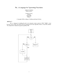
1
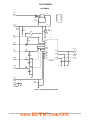
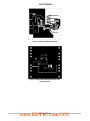
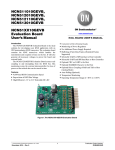
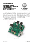
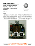
NCV7703GEVB
NCV7703 Evaluation Board
User's Manual
http://onsemi.com
EVAL BOARD USER’S MANUAL
Description
•
•
•
•
•
•
•
•
•
•
The NCV7703 is a fully−protected triple half−bridge
driver designed specifically for automotive and industrial
motion control applications. The three half-bridge drivers
have independent control. This allows for high-side, low
side, and H-Bridge control. H-Bridge control provides
forward, reverse, brake, and high impedance states.
Driver control is accomplished via a standard Serial
Peripheral Interface (SPI).
The Evaluation Board includes both an NCV7703 and
NCV8501 5 V regulator. By means of a jumper, the user can
select an on−board or external VCC source for the IC.
Numerous convenient terminal points are provided to
accommodate multiple application configurations.
•
•
•
Features
• Ultra Low Quiescent Current in Sleep Mode
• Three High-Side and Three Low-Side Drivers
Internal Free-wheeling Clamp Diodes
Configurable as H-Bridge Drivers
0.5 A Continuous (1 A peak) Current
Rdson = 0.8 W (typ)
5 MHz SPI Control with Daisy Chain Capability
Compliance with 5 V and 3.3 V Systems
Over Voltage Lockout
Under Voltage Lockout
Fault Reporting
1.4 A Over Current Threshold Detection with Optional
Shutdown
3 A Current Limit with Auto Shutdown
Over Temperature Warning and Protection Levels
Internally Fused Leads in SON-14 Package
Connected as Half-Bridges
Figure 1. Evaluation Board Photo
www.BDTIC.com/ON/
© Semiconductor Components Industries, LLC, 2012
May, 2012 − Rev. 2
Figure 2. Silkscreen Showing Component
Positions of the NCV7703GEVB
1
Publication Order Number:
EVBUM2115/D
NCV7703GEVB
SCHEMATIC
VB+
1
R3
10k
U2
Vin
Vout
MON
/Flag
EN
/Reset
45
Delay GND
2
3
+5V
8
7
6
GND
GND
OUT3
VS
OUT1
OUT2
Vcc
EN
CSB
SI
NCV8501
C22
0.1uF
SCLK
SO
GND
GND
Pinout
5V
Vcc
R9
100k
C12
0.1uF
D1
LEDSM
EN
R4
470
R1
1k
EN
U1
R8
100k
SO
EN
SO
5
SI
6
SCLK
CSB
4
R7
100
C16
10pF
SCLK
VCC
10
9
R2
100
SI
11
3
VS
1
GND
7
8
14
R6
OUT1
OUT1
13
GND
OUT2
12
GND
GND
OUT3
2
100
OUT2
OUT3
NCV7703
C15
10pF
CSB
C7
C2
10nF 10nF
C3
10nF
R5
100
C14
10pF
VB+
GND
C5
330uF
GND
Figure 3. Evaluation Board Schematic
www.BDTIC.com/ON/
http://onsemi.com
2
NCV7703GEVB
Notice the SO of the SPI controller connects to the SI of
the NCV7703GEVB, and the SO of the NCV7703GEVB
connects to the SI of the SPI controller.
The Enable jumper hard wires the Enable pin (EN) to be
on. The Enable function may also be provided by the SPI
Controller. Disconnect the Enable jumper when providing
the signal externally.
Refer to the data sheet for SPI interface functionality.
Typical connections to the evaluation board are shown in
Figure 4. The diagram illustrates half-bridge operation of a
motor, and the option for a high-side or low-side load. The
load connections are for illustration only and do not limit
other possible connections.
The connection of the battery or supply (to VB+) powers
the board. VCC for the NCV7703 may be powered by the
on−board regulator (powered from VB+) with the 5 V
jumper. Remove the 5 V jumper if powering from an
external source. LED D1 indicates when 5 V is present
(powered on-board or externally).
Figure 4. Typical NCV7703 Power Connections
SPI Communication
3. CSB goes high to transfer the clocked in
information to the data registers.
Note SO is tristate when CSB is high.
4. The SI data will be accepted when a valid SPI
frame is detected. A valid SPI frame consists of
the above conditions and a complete set of
multiples of 16 bit words.
Standard 16-bit communication has been implemented
for the communication of this IC to turn drivers on and off,
and to report faults. The LSB (Least Significant Bit) is
clocked in first.
Communication is implemented as follows:
1. CSB goes low to allow serial data transfer.
2. A 16 bit word is clocked (SCLK) into the SI
(Serial Input) pin.
www.BDTIC.com/ON/
http://onsemi.com
3
NCV7703GEVB
SPI Communication Frame Format
chain communication between SPI compatible IC’s is
possible by connection of the Serial Output pin (SO) to the
input of the sequential IC (SI).
The table below defines the programming bits and
diagnostic bits. Fault information is sequentially clocked
out the SO pin of the NCV7703 as programming
information is clocked into the SI pin of the device. Daisy
Table 1. PROGRAMMING AND DIAGNOSTIC BITS
Input Data
Bit
Number
15
Output Data
Bit Description
Bit Status
Bit
Number
Over Voltage Lock Out Control
(OVLO)
0 = Disable
15
14
Not Used
13
Over Current Detection Shut
Down Control (OCD)
Bit Description
Bit Status
Power Supply Fail Signal
(PSF for OVLO or UVLO)
0 = No Fault
14
Under Load Detect Signal
(ULD)
0 = No Fault
13
Over Load Detect Signal
(OLD)
0 = No Fault
1 = Enable
0 = Disable
1 = Enable
12
Not Used
12
Not Used
11
Not Used
11
Not Used
10
Not Used
10
Not Used
9
Not Used
9
Not Used
8
Not Used
8
Not Used
7
Not Used
7
Not Used
6
OUTH3
6
OUTH3
0 = Off
1 = On
5
OUTL3
4
OUTH2
0 = Off
5
OUTL3
4
OUTH2
OUTH1
3
0 = Off
OUTL2
OUTL1
2
0 = Off
OUTH1
Status Register Reset (SRR)
0 = Off
0 = Off
0 = Off
1 = On
1
0 = Off
OUTL1
1 = On
0
0 = Off
1 = On
1 = On
1
0 = Off
1 = On
1 = On
2
1 = Fault
1 = On
0 = Off
1 = On
OUTL2
1 = Fault
1 = On
1 = On
3
1 = Fault
0 = Off
1 = On
0
0 = No Reset
Thermal Warning (TW)
1 = Reset
0 = Not in TW
1 = In TW
Operational Recommendations
Recommended operating voltages for this board are:
Vbat+ = 13.2 V
VCC = 5 V.
This board is not reverse battery protected. Damage to the
board may occur with incorrect connections. The NCV7703
device and C5 (aluminum electrolytic capacitor) are
particularly sensitive to reverse battery conditions. See the
NCV7703/D datasheet for electrical and environmental
testing limits.
www.BDTIC.com/ON/
http://onsemi.com
4
NCV7703GEVB
Figure 5. Component Side Etch Pattern
Figure 6. Reverse Side Etch Pattern Shown from
Component Side
www.BDTIC.com/ON/
http://onsemi.com
5
NCV7703GEVB
BILL OF MATERIALS
ON Semiconductor and
are registered trademarks of Semiconductor Components Industries, LLC (SCILLC). SCILLC reserves the right to make changes without further notice
to any products herein. SCILLC makes no warranty, representation or guarantee regarding the suitability of its products for any particular purpose, nor does SCILLC assume any liability
arising out of the application or use of any product or circuit, and specifically disclaims any and all liability, including without limitation special, consequential or incidental damages.
“Typical” parameters which may be provided in SCILLC data sheets and/or specifications can and do vary in different applications and actual performance may vary over time. All
operating parameters, including “Typicals” must be validated for each customer application by customer’s technical experts. SCILLC does not convey any license under its patent rights
nor the rights of others. SCILLC products are not designed, intended, or authorized for use as components in systems intended for surgical implant into the body, or other applications
intended to support or sustain life, or for any other application in which the failure of the SCILLC product could create a situation where personal injury or death may occur. Should
Buyer purchase or use SCILLC products for any such unintended or unauthorized application, Buyer shall indemnify and hold SCILLC and its officers, employees, subsidiaries, affiliates,
and distributors harmless against all claims, costs, damages, and expenses, and reasonable attorney fees arising out of, directly or indirectly, any claim of personal injury or death
associated with such unintended or unauthorized use, even if such claim alleges that SCILLC was negligent regarding the design or manufacture of the part. SCILLC is an Equal
Opportunity/Affirmative Action Employer. This literature is subject to all applicable copyright laws and is not for resale in any manner.
PUBLICATION ORDERING INFORMATION
LITERATURE FULFILLMENT:
Literature Distribution Center for ON Semiconductor
P.O. Box 5163, Denver, Colorado 80217 USA
Phone: 303−675−2175 or 800−344−3860 Toll Free USA/Canada
Fax: 303−675−2176 or 800−344−3867 Toll Free USA/Canada
Email: [email protected]
N. American Technical Support: 800−282−9855 Toll Free
USA/Canada
Europe, Middle East and Africa Technical Support:
Phone: 421 33 790 2910
Japan Customer Focus Center
Phone: 81−3−5817−1050
ON Semiconductor Website: www.onsemi.com
Order Literature: http://www.onsemi.com/orderlit
For additional information, please contact your local
Sales Representative
www.BDTIC.com/ON/
http://onsemi.com
6
EVBUM2115/D