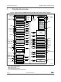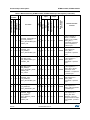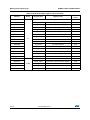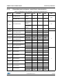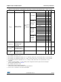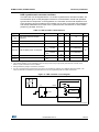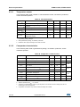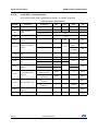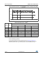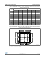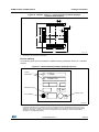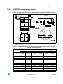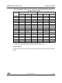
1
STM8L151x4, STM8L151x6, STM8L152x4, STM8L152x6 8-bit ultra-low-power MCU, up to 32 KB Flash, 1 KB Data EEPROM, RTC, LCD, timers, USART, I2C, SPI, ADC, DAC, comparators Datasheet - production data Features • Operating conditions – Operating power supply range 1.8 V to 3.6 V (down to 1.65 V at power down) – Temp. range: - 40 °C to 85, 105 or 125 °C • Low power features – 5 low power modes: Wait, Low power run (5.1 µA), Low power wait (3 µA), Active-halt with full RTC (1.3 µA), Halt (350 nA) – Consumption: 195 µA/MHz + 440 µA – Ultra-low leakage per I/0: 50 nA – Fast wakeup from Halt: 4.7 µs • Advanced STM8 core – Harvard architecture and 3-stage pipeline – Max freq. 16 MHz, 16 CISC MIPS peak – Up to 40 external interrupt sources • Reset and supply management – Low power, ultra-safe BOR reset with 5 selectable thresholds – Ultra-low-power POR/PDR – Programmable voltage detector (PVD) • Clock management – 1 to 16 MHz crystal oscillator – 32 kHz crystal oscillator – Internal 16 MHz factory-trimmed RC – Internal 38 kHz low consumption RC – Clock security system • Low power RTC – BCD calendar with alarm interrupt – Auto-wakeup from Halt w/ periodic interrupt • LCD: up to 4x28 segments w/ step-up converter • Memories – Up to 32 KB of Flash program memory and 1 Kbyte of data EEPROM with ECC, RWW – Flexible write and read protection modes – Up to 2 Kbyte of RAM • DMA – 4 channels; supported peripherals: ADC, DAC, SPI, I2C, USART, timers – 1 channel for memory-to-memory April 2015 This is information on a product in full production. UFQFPN48 7x7 mm LQFP48 7x7 mm UFQFPN32 (5x5 mm) LQFP32 7x7 mm UFQFPN28 (4x4 mm) #30 WLCSP28 • 12-bit DAC with output buffer • 12-bit ADC up to 1 Msps/25 channels – T. sensor and internal reference voltage • 2 ultra-low-power comparators – 1 with fixed threshold and 1 rail to rail – Wakeup capability • Timers – Two 16-bit timers with 2 channels (used as IC, OC, PWM), quadrature encoder – One 16-bit advanced control timer with 3 channels, supporting motor control – One 8-bit timer with 7-bit prescaler – 2 watchdogs: 1 Window, 1 Independent – Beeper timer with 1, 2 or 4 kHz frequencies • Communication interfaces – Synchronous serial interface (SPI) – Fast I2C 400 kHz SMBus and PMBus – USART (ISO 7816 interface and IrDA) • Up to 41 I/Os, all mappable on interrupt vectors • Up to 16 capacitive sensing channels supporting touchkey, proximity, linear touch and rotary touch sensors • Development support – Fast on-chip programming and non intrusive debugging with SWIM – Bootloader using USART • 96-bit unique ID Table 1. Device summary Reference Part number STM8L151xx (without LCD) STM8L151C4, STM8L151C6, STM8L151K4, STM8L151K6, STM8L151G4, STM8L151G6 STM8L152xx (with LCD) STM8L152C4, STM8L152C6, STM8L152K4, STM8L152K6 DocID15962 Rev 14 1/142 www.st.com Contents STM8L151x4/6, STM8L152x4/6 Contents 1 Introduction . . . . . . . . . . . . . . . . . . . . . . . . . . . . . . . . . . . . . . . . . . . . . . . . 9 2 Description . . . . . . . . . . . . . . . . . . . . . . . . . . . . . . . . . . . . . . . . . . . . . . . . 11 3 2.1 Device overview . . . . . . . . . . . . . . . . . . . . . . . . . . . . . . . . . . . . . . . . . . . . 12 2.2 Ultra-low-power continuum . . . . . . . . . . . . . . . . . . . . . . . . . . . . . . . . . . . . 13 Functional overview . . . . . . . . . . . . . . . . . . . . . . . . . . . . . . . . . . . . . . . . 14 3.1 Low-power modes . . . . . . . . . . . . . . . . . . . . . . . . . . . . . . . . . . . . . . . . . . 15 3.2 Central processing unit STM8 . . . . . . . . . . . . . . . . . . . . . . . . . . . . . . . . . 16 3.3 Advanced STM8 Core . . . . . . . . . . . . . . . . . . . . . . . . . . . . . . . . . . . . . . 16 3.2.2 Interrupt controller . . . . . . . . . . . . . . . . . . . . . . . . . . . . . . . . . . . . . . . . . 16 Reset and supply management . . . . . . . . . . . . . . . . . . . . . . . . . . . . . . . . 17 3.3.1 Power supply scheme . . . . . . . . . . . . . . . . . . . . . . . . . . . . . . . . . . . . . . 17 3.3.2 Power supply supervisor . . . . . . . . . . . . . . . . . . . . . . . . . . . . . . . . . . . . 17 3.3.3 Voltage regulator . . . . . . . . . . . . . . . . . . . . . . . . . . . . . . . . . . . . . . . . . . 17 3.4 Clock management . . . . . . . . . . . . . . . . . . . . . . . . . . . . . . . . . . . . . . . . . 18 3.5 Low power real-time clock . . . . . . . . . . . . . . . . . . . . . . . . . . . . . . . . . . . . 19 3.6 LCD (Liquid crystal display) . . . . . . . . . . . . . . . . . . . . . . . . . . . . . . . . . . . 20 3.7 Memories . . . . . . . . . . . . . . . . . . . . . . . . . . . . . . . . . . . . . . . . . . . . . . . . . 20 3.8 DMA . . . . . . . . . . . . . . . . . . . . . . . . . . . . . . . . . . . . . . . . . . . . . . . . . . . . . 20 3.9 Analog-to-digital converter . . . . . . . . . . . . . . . . . . . . . . . . . . . . . . . . . . . . 20 3.10 Digital-to-analog converter (DAC) . . . . . . . . . . . . . . . . . . . . . . . . . . . . . . 21 3.11 Ultra-low-power comparators . . . . . . . . . . . . . . . . . . . . . . . . . . . . . . . . . . 21 3.12 System configuration controller and routing interface . . . . . . . . . . . . . . . 21 3.13 Touch sensing . . . . . . . . . . . . . . . . . . . . . . . . . . . . . . . . . . . . . . . . . . . . . 21 3.14 Timers . . . . . . . . . . . . . . . . . . . . . . . . . . . . . . . . . . . . . . . . . . . . . . . . . . . 22 3.15 2/142 3.2.1 3.14.1 TIM1 - 16-bit advanced control timer . . . . . . . . . . . . . . . . . . . . . . . . . . . 22 3.14.2 16-bit general purpose timers . . . . . . . . . . . . . . . . . . . . . . . . . . . . . . . . 23 3.14.3 8-bit basic timer . . . . . . . . . . . . . . . . . . . . . . . . . . . . . . . . . . . . . . . . . . . 23 Watchdog timers . . . . . . . . . . . . . . . . . . . . . . . . . . . . . . . . . . . . . . . . . . . 23 3.15.1 Window watchdog timer . . . . . . . . . . . . . . . . . . . . . . . . . . . . . . . . . . . . . 23 3.15.2 Independent watchdog timer . . . . . . . . . . . . . . . . . . . . . . . . . . . . . . . . . 23 DocID15962 Rev 14 STM8L151x4/6, STM8L152x4/6 4 3.16 Beeper . . . . . . . . . . . . . . . . . . . . . . . . . . . . . . . . . . . . . . . . . . . . . . . . . . . 23 3.17 Communication interfaces . . . . . . . . . . . . . . . . . . . . . . . . . . . . . . . . . . . . 24 3.17.1 SPI . . . . . . . . . . . . . . . . . . . . . . . . . . . . . . . . . . . . . . . . . . . . . . . . . . . . . 24 3.17.2 I²C . . . . . . . . . . . . . . . . . . . . . . . . . . . . . . . . . . . . . . . . . . . . . . . . . . . . . 24 3.17.3 USART . . . . . . . . . . . . . . . . . . . . . . . . . . . . . . . . . . . . . . . . . . . . . . . . . . 24 3.18 Infrared (IR) interface . . . . . . . . . . . . . . . . . . . . . . . . . . . . . . . . . . . . . . . . 24 3.19 Development support . . . . . . . . . . . . . . . . . . . . . . . . . . . . . . . . . . . . . . . . 25 Pinout and pin description . . . . . . . . . . . . . . . . . . . . . . . . . . . . . . . . . . . 26 4.1 5 Contents System configuration options . . . . . . . . . . . . . . . . . . . . . . . . . . . . . . . . . . 37 Memory and register map . . . . . . . . . . . . . . . . . . . . . . . . . . . . . . . . . . . . 38 5.1 Memory mapping . . . . . . . . . . . . . . . . . . . . . . . . . . . . . . . . . . . . . . . . . . . 38 5.2 Register map . . . . . . . . . . . . . . . . . . . . . . . . . . . . . . . . . . . . . . . . . . . . . . 39 6 Interrupt vector mapping . . . . . . . . . . . . . . . . . . . . . . . . . . . . . . . . . . . . 57 7 Option bytes . . . . . . . . . . . . . . . . . . . . . . . . . . . . . . . . . . . . . . . . . . . . . . 59 8 Unique ID . . . . . . . . . . . . . . . . . . . . . . . . . . . . . . . . . . . . . . . . . . . . . . . . . 62 9 Electrical parameters . . . . . . . . . . . . . . . . . . . . . . . . . . . . . . . . . . . . . . . 63 9.1 Parameter conditions . . . . . . . . . . . . . . . . . . . . . . . . . . . . . . . . . . . . . . . . 63 9.1.1 Minimum and maximum values . . . . . . . . . . . . . . . . . . . . . . . . . . . . . . . 63 9.1.2 Typical values . . . . . . . . . . . . . . . . . . . . . . . . . . . . . . . . . . . . . . . . . . . . 63 9.1.3 Typical curves . . . . . . . . . . . . . . . . . . . . . . . . . . . . . . . . . . . . . . . . . . . . 63 9.1.4 Loading capacitor . . . . . . . . . . . . . . . . . . . . . . . . . . . . . . . . . . . . . . . . . 63 9.1.5 Pin input voltage . . . . . . . . . . . . . . . . . . . . . . . . . . . . . . . . . . . . . . . . . . 64 9.2 Absolute maximum ratings . . . . . . . . . . . . . . . . . . . . . . . . . . . . . . . . . . . . 64 9.3 Operating conditions . . . . . . . . . . . . . . . . . . . . . . . . . . . . . . . . . . . . . . . . 66 9.3.1 General operating conditions . . . . . . . . . . . . . . . . . . . . . . . . . . . . . . . . . 66 9.3.2 Embedded reset and power control block characteristics . . . . . . . . . . . 67 9.3.3 Supply current characteristics . . . . . . . . . . . . . . . . . . . . . . . . . . . . . . . . 68 9.3.4 Clock and timing characteristics . . . . . . . . . . . . . . . . . . . . . . . . . . . . . . 82 9.3.5 Memory characteristics . . . . . . . . . . . . . . . . . . . . . . . . . . . . . . . . . . . . . 88 9.3.6 I/O current injection characteristics . . . . . . . . . . . . . . . . . . . . . . . . . . . . 89 9.3.7 I/O port pin characteristics . . . . . . . . . . . . . . . . . . . . . . . . . . . . . . . . . . . 89 DocID15962 Rev 14 3/142 4 Contents 10 STM8L151x4/6, STM8L152x4/6 9.3.8 Communication interfaces . . . . . . . . . . . . . . . . . . . . . . . . . . . . . . . . . . . 97 9.3.9 LCD controller (STM8L152xx only) . . . . . . . . . . . . . . . . . . . . . . . . . . . 102 9.3.10 Embedded reference voltage . . . . . . . . . . . . . . . . . . . . . . . . . . . . . . . . 103 9.3.11 Temperature sensor . . . . . . . . . . . . . . . . . . . . . . . . . . . . . . . . . . . . . . . 104 9.3.12 Comparator characteristics . . . . . . . . . . . . . . . . . . . . . . . . . . . . . . . . . 104 9.3.13 12-bit DAC characteristics . . . . . . . . . . . . . . . . . . . . . . . . . . . . . . . . . . 106 9.3.14 12-bit ADC1 characteristics . . . . . . . . . . . . . . . . . . . . . . . . . . . . . . . . . 108 9.3.15 EMC characteristics . . . . . . . . . . . . . . . . . . . . . . . . . . . . . . . . . . . . . . . 114 Package information . . . . . . . . . . . . . . . . . . . . . . . . . . . . . . . . . . . . . . . 116 10.1 ECOPACK . . . . . . . . . . . . . . . . . . . . . . . . . . . . . . . . . . . . . . . . . . . . . . . .116 10.2 LQFP48 package information . . . . . . . . . . . . . . . . . . . . . . . . . . . . . . . . . .116 10.3 UFQFPN48 package information . . . . . . . . . . . . . . . . . . . . . . . . . . . . . . 120 10.4 LQFP32 package information . . . . . . . . . . . . . . . . . . . . . . . . . . . . . . . . . 123 10.5 UFQFPN32 package information . . . . . . . . . . . . . . . . . . . . . . . . . . . . . . 126 10.6 UFQFPN28 package information . . . . . . . . . . . . . . . . . . . . . . . . . . . . . . 129 10.7 WLCSP28 package information . . . . . . . . . . . . . . . . . . . . . . . . . . . . . . . 132 10.8 Thermal characteristics . . . . . . . . . . . . . . . . . . . . . . . . . . . . . . . . . . . . . 135 11 Part numbering . . . . . . . . . . . . . . . . . . . . . . . . . . . . . . . . . . . . . . . . . . . 136 12 Revision history . . . . . . . . . . . . . . . . . . . . . . . . . . . . . . . . . . . . . . . . . . 137 4/142 DocID15962 Rev 14 STM8L151x4/6, STM8L152x4/6 List of tables List of tables Table 1. Table 2. Table 3. Table 4. Table 5. Table 6. Table 7. Table 8. Table 9. Table 10. Table 11. Table 12. Table 13. Table 14. Table 15. Table 16. Table 17. Table 18. Table 19. Table 20. Table 21. Table 22. Table 23. Table 24. Table 25. Table 26. Table 27. Table 28. Table 29. Table 30. Table 31. Table 32. Table 33. Table 34. Table 35. Table 36. Table 37. Table 38. Table 39. Table 40. Table 41. Table 42. Table 43. Table 44. Table 45. Table 46. Device summary . . . . . . . . . . . . . . . . . . . . . . . . . . . . . . . . . . . . . . . . . . . . . . . . . . . . . . . . . . 1 Medium-density STM8L151x4/6 and STM8L152x4/6 low-power device features and peripheral counts . . . . . . . . . . . . . . . . . . . . . . . . . . . . . . . . . . . . . . . . . . . . . . . . . . . . . . . . 12 Timer feature comparison . . . . . . . . . . . . . . . . . . . . . . . . . . . . . . . . . . . . . . . . . . . . . . . . . . 22 Legend/abbreviation for table 5 . . . . . . . . . . . . . . . . . . . . . . . . . . . . . . . . . . . . . . . . . . . . . 29 Medium-density STM8L151x4/6, STM8L152x4/6 pin description. . . . . . . . . . . . . . . . . . . . 29 Flash and RAM boundary addresses . . . . . . . . . . . . . . . . . . . . . . . . . . . . . . . . . . . . . . . . . 39 Factory conversion registers. . . . . . . . . . . . . . . . . . . . . . . . . . . . . . . . . . . . . . . . . . . . . . . . 39 I/O port hardware register map . . . . . . . . . . . . . . . . . . . . . . . . . . . . . . . . . . . . . . . . . . . . . . 39 General hardware register map . . . . . . . . . . . . . . . . . . . . . . . . . . . . . . . . . . . . . . . . . . . . . 40 CPU/SWIM/debug module/interrupt controller registers . . . . . . . . . . . . . . . . . . . . . . . . . . . 55 Interrupt mapping . . . . . . . . . . . . . . . . . . . . . . . . . . . . . . . . . . . . . . . . . . . . . . . . . . . . . . . . 57 Option byte addresses . . . . . . . . . . . . . . . . . . . . . . . . . . . . . . . . . . . . . . . . . . . . . . . . . . . . 59 Option byte description . . . . . . . . . . . . . . . . . . . . . . . . . . . . . . . . . . . . . . . . . . . . . . . . . . . . 60 Unique ID registers (96 bits) . . . . . . . . . . . . . . . . . . . . . . . . . . . . . . . . . . . . . . . . . . . . . . . . 62 Voltage characteristics . . . . . . . . . . . . . . . . . . . . . . . . . . . . . . . . . . . . . . . . . . . . . . . . . . . . 64 Current characteristics . . . . . . . . . . . . . . . . . . . . . . . . . . . . . . . . . . . . . . . . . . . . . . . . . . . . 65 Thermal characteristics. . . . . . . . . . . . . . . . . . . . . . . . . . . . . . . . . . . . . . . . . . . . . . . . . . . . 65 General operating conditions . . . . . . . . . . . . . . . . . . . . . . . . . . . . . . . . . . . . . . . . . . . . . . . 66 Embedded reset and power control block characteristics. . . . . . . . . . . . . . . . . . . . . . . . . . 67 Total current consumption in Run mode . . . . . . . . . . . . . . . . . . . . . . . . . . . . . . . . . . . . . . . 69 Total current consumption in Wait mode . . . . . . . . . . . . . . . . . . . . . . . . . . . . . . . . . . . . . . 71 Total current consumption and timing in Low power run mode at VDD = 1.65 V to 3.6 V . . . . . . . . . . . . . . . . . . . . . . . . . . . . . . . . . . . . . . . . . . . . . . . . . . 74 Total current consumption in Low power wait mode at VDD = 1.65 V to 3.6 V . . . . . . . . . 76 Total current consumption and timing in Active-halt mode at VDD = 1.65 V to 3.6 V. . . . . 78 Typical current consumption in Active-halt mode, RTC clocked by LSE external crystal . . 80 Total current consumption and timing in Halt mode at VDD = 1.65 to 3.6 V . . . . . . . . . . . 80 Peripheral current consumption . . . . . . . . . . . . . . . . . . . . . . . . . . . . . . . . . . . . . . . . . . . . . 81 Current consumption under external reset . . . . . . . . . . . . . . . . . . . . . . . . . . . . . . . . . . . . . 82 HSE external clock characteristics . . . . . . . . . . . . . . . . . . . . . . . . . . . . . . . . . . . . . . . . . . . 82 LSE external clock characteristics . . . . . . . . . . . . . . . . . . . . . . . . . . . . . . . . . . . . . . . . . . . 82 HSE oscillator characteristics . . . . . . . . . . . . . . . . . . . . . . . . . . . . . . . . . . . . . . . . . . . . . . . 83 LSE oscillator characteristics . . . . . . . . . . . . . . . . . . . . . . . . . . . . . . . . . . . . . . . . . . . . . . . 84 HSI oscillator characteristics. . . . . . . . . . . . . . . . . . . . . . . . . . . . . . . . . . . . . . . . . . . . . . . . 85 LSI oscillator characteristics . . . . . . . . . . . . . . . . . . . . . . . . . . . . . . . . . . . . . . . . . . . . . . . . 86 RAM and hardware registers . . . . . . . . . . . . . . . . . . . . . . . . . . . . . . . . . . . . . . . . . . . . . . . 88 Flash program and data EEPROM memory . . . . . . . . . . . . . . . . . . . . . . . . . . . . . . . . . . . . 88 I/O current injection susceptibility . . . . . . . . . . . . . . . . . . . . . . . . . . . . . . . . . . . . . . . . . . . . 89 I/O static characteristics . . . . . . . . . . . . . . . . . . . . . . . . . . . . . . . . . . . . . . . . . . . . . . . . . . . 90 Output driving current (high sink ports). . . . . . . . . . . . . . . . . . . . . . . . . . . . . . . . . . . . . . . . 93 Output driving current (true open drain ports). . . . . . . . . . . . . . . . . . . . . . . . . . . . . . . . . . . 93 Output driving current (PA0 with high sink LED driver capability). . . . . . . . . . . . . . . . . . . . 93 NRST pin characteristics . . . . . . . . . . . . . . . . . . . . . . . . . . . . . . . . . . . . . . . . . . . . . . . . . . 95 SPI1 characteristics . . . . . . . . . . . . . . . . . . . . . . . . . . . . . . . . . . . . . . . . . . . . . . . . . . . . . . 97 I2C characteristics . . . . . . . . . . . . . . . . . . . . . . . . . . . . . . . . . . . . . . . . . . . . . . . . . . . . . . 100 LCD characteristics. . . . . . . . . . . . . . . . . . . . . . . . . . . . . . . . . . . . . . . . . . . . . . . . . . . . . . 102 Reference voltage characteristics. . . . . . . . . . . . . . . . . . . . . . . . . . . . . . . . . . . . . . . . . . . 103 DocID15962 Rev 14 5/142 6 List of tables Table 47. Table 48. Table 49. Table 50. Table 51. Table 52. Table 53. Table 54. Table 55. Table 56. Table 57. Table 58. Table 59. Table 60. Table 61. Table 62. Table 63. Table 64. Table 65. Table 66. Table 67. Table 68. Table 69. 6/142 STM8L151x4/6, STM8L152x4/6 TS characteristics . . . . . . . . . . . . . . . . . . . . . . . . . . . . . . . . . . . . . . . . . . . . . . . . . . . . . . . 104 Comparator 1 characteristics . . . . . . . . . . . . . . . . . . . . . . . . . . . . . . . . . . . . . . . . . . . . . . 104 Comparator 2 characteristics . . . . . . . . . . . . . . . . . . . . . . . . . . . . . . . . . . . . . . . . . . . . . . 105 DAC characteristics . . . . . . . . . . . . . . . . . . . . . . . . . . . . . . . . . . . . . . . . . . . . . . . . . . . . . 106 DAC accuracy . . . . . . . . . . . . . . . . . . . . . . . . . . . . . . . . . . . . . . . . . . . . . . . . . . . . . . . . . . 107 DAC output on PB4-PB5-PB6 . . . . . . . . . . . . . . . . . . . . . . . . . . . . . . . . . . . . . . . . . . . . . 107 ADC1 characteristics . . . . . . . . . . . . . . . . . . . . . . . . . . . . . . . . . . . . . . . . . . . . . . . . . . . . 108 ADC1 accuracy with VDDA = 3.3 V to 2.5 V. . . . . . . . . . . . . . . . . . . . . . . . . . . . . . . . . . . 110 ADC1 accuracy with VDDA = 2.4 V to 3.6 V. . . . . . . . . . . . . . . . . . . . . . . . . . . . . . . . . . . 110 ADC1 accuracy with VDDA = VREF+ = 1.8 V to 2.4 V. . . . . . . . . . . . . . . . . . . . . . . . . . . 110 RAIN max for fADC = 16 MHz . . . . . . . . . . . . . . . . . . . . . . . . . . . . . . . . . . . . . . . . . . . . . . . 112 EMS data . . . . . . . . . . . . . . . . . . . . . . . . . . . . . . . . . . . . . . . . . . . . . . . . . . . . . . . . . . . . . 114 EMI data . . . . . . . . . . . . . . . . . . . . . . . . . . . . . . . . . . . . . . . . . . . . . . . . . . . . . . . . . . . . . 115 ESD absolute maximum ratings . . . . . . . . . . . . . . . . . . . . . . . . . . . . . . . . . . . . . . . . . . . . 115 Electrical sensitivities . . . . . . . . . . . . . . . . . . . . . . . . . . . . . . . . . . . . . . . . . . . . . . . . . . . . 115 LQFP48 - 48-pin, 7 x 7 mm low-profile quad flat package mechanical data . . . . . . . . . . . . . . . . . . . . . . . . . . . . . . . . . . . . . . . . . . . . . . . . . . . . . . . . 117 UFQFPN48 - 48-lead, 7 x 7 mm, 0.5 mm pitch, ultra thin fine pitch quad flat package mechanical data . . . . . . . . . . . . . . . . . . . . . . . . . . . . . . . . . . . . . . . . . . . . . . . . . 121 LQFP32 - 32-pin, 7 x 7 mm low-profile quad flat package mechanical data . . . . . . . . . . . . . . . . . . . . . . . . . . . . . . . . . . . . . . . . . . . . . . . . . . . . . . . . 124 UFQFPN32 - 32-pin, 5 x 5 mm, 0.5 mm pitch ultra thin fine pitch quad flat package mechanical data . . . . . . . . . . . . . . . . . . . . . . . . . . . . . . . . . . . . . . . . . . . . . . . . . 127 UFQFPN28 - 28-lead, 4 x 4 mm, 0.5 mm pitch, ultra thin fine pitch quad flat package mechanical data . . . . . . . . . . . . . . . . . . . . . . . . . . . . . . . . . . . . . . . . . . . . . . . . . 129 WLCSP28 - 28-pin, 1.703 x 2.841 mm, 0.4 mm pitch wafer level chip scale package mechanical data . . . . . . . . . . . . . . . . . . . . . . . . . . . . . . . . . . . . . . . . . . . . . . . . . 133 Thermal characteristics. . . . . . . . . . . . . . . . . . . . . . . . . . . . . . . . . . . . . . . . . . . . . . . . . . . 135 Document revision history . . . . . . . . . . . . . . . . . . . . . . . . . . . . . . . . . . . . . . . . . . . . . . . . 137 DocID15962 Rev 14 STM8L151x4/6, STM8L152x4/6 List of figures List of figures Figure 1. Figure 2. Figure 3. Figure 4. Figure 5. Figure 6. Figure 7. Figure 8. Figure 9. Figure 10. Figure 11. Figure 12. Figure 13. Figure 14. Figure 15. Figure 16. Figure 17. Figure 18. Figure 19. Figure 20. Figure 21. Figure 22. Figure 23. Figure 24. Figure 25. Figure 26. Figure 27. Figure 28. Figure 29. Figure 30. Figure 31. Figure 32. Figure 33. Figure 34. Figure 35. Figure 36. Figure 37. Figure 38. Figure 39. Figure 40. Figure 41. Figure 42. Figure 43. Figure 44. Figure 45. Figure 46. Medium-density STM8L151x4/6 and STM8L152x4/6 device block diagram . . . . . . . . . . . 14 Medium-density STM8L151x4/6 and STM8L152x4/6 clock tree diagram . . . . . . . . . . . . . 19 STM8L151C4, STM8L151C6 48-pin pinout (without LCD). . . . . . . . . . . . . . . . . . . . . . . . . 26 STM8L151K4, STM8L151K6 32-pin package pinout (without LCD). . . . . . . . . . . . . . . . . . 26 STM8L151Gx UFQFPN28 package pinout . . . . . . . . . . . . . . . . . . . . . . . . . . . . . . . . . . . . 26 STM8L151G4, STM8L151G6 WLCSP28 package pinout . . . . . . . . . . . . . . . . . . . . . . . . . 27 STM8L152C4, STM8L152C6 48-pin pinout (with LCD) . . . . . . . . . . . . . . . . . . . . . . . . . . . 27 STM8L152K4, STM8L152K6 32-pin package pinout (with LCD) . . . . . . . . . . . . . . . . . . . . 28 Memory map . . . . . . . . . . . . . . . . . . . . . . . . . . . . . . . . . . . . . . . . . . . . . . . . . . . . . . . . . . . 38 Pin loading conditions . . . . . . . . . . . . . . . . . . . . . . . . . . . . . . . . . . . . . . . . . . . . . . . . . . . . . 63 Pin input voltage . . . . . . . . . . . . . . . . . . . . . . . . . . . . . . . . . . . . . . . . . . . . . . . . . . . . . . . . . 64 POR/BOR thresholds . . . . . . . . . . . . . . . . . . . . . . . . . . . . . . . . . . . . . . . . . . . . . . . . . . . . . 68 Typ. IDD(RUN) vs. VDD, fCPU = 16 MHz . . . . . . . . . . . . . . . . . . . . . . . . . . . . . . . . . . . . . 70 Typ. IDD(Wait) vs. VDD, fCPU = 16 MHz 1). . . . . . . . . . . . . . . . . . . . . . . . . . . . . . . . . . . . 73 Typ. IDD(LPR) vs. VDD (LSI clock source) . . . . . . . . . . . . . . . . . . . . . . . . . . . . . . . . . . . . 75 Typ. IDD(LPW) vs. VDD (LSI clock source) . . . . . . . . . . . . . . . . . . . . . . . . . . . . . . . . . . . . 77 HSE oscillator circuit diagram . . . . . . . . . . . . . . . . . . . . . . . . . . . . . . . . . . . . . . . . . . . . . . . 83 LSE oscillator circuit diagram . . . . . . . . . . . . . . . . . . . . . . . . . . . . . . . . . . . . . . . . . . . . . . . 85 Typical HSI frequency vs VDD. . . . . . . . . . . . . . . . . . . . . . . . . . . . . . . . . . . . . . . . . . . . . . . 86 Typical LSI frequency vs. VDD . . . . . . . . . . . . . . . . . . . . . . . . . . . . . . . . . . . . . . . . . . . . . 87 Typical VIL and VIH vs VDD (high sink I/Os) . . . . . . . . . . . . . . . . . . . . . . . . . . . . . . . . . . . 91 Typical VIL and VIH vs VDD (true open drain I/Os) . . . . . . . . . . . . . . . . . . . . . . . . . . . . . . 91 Typical pull-up resistance RPU vs VDD with VIN=VSS . . . . . . . . . . . . . . . . . . . . . . . . . . . . 92 Typical pull-up current Ipu vs VDD with VIN=VSS . . . . . . . . . . . . . . . . . . . . . . . . . . . . . . . . 92 Typ. VOL @ VDD = 3.0 V (high sink ports) . . . . . . . . . . . . . . . . . . . . . . . . . . . . . . . . . . . . 94 Typ. VOL @ VDD = 1.8 V (high sink ports) . . . . . . . . . . . . . . . . . . . . . . . . . . . . . . . . . . . . 94 Typ. VOL @ VDD = 3.0 V (true open drain ports) . . . . . . . . . . . . . . . . . . . . . . . . . . . . . . . 94 Typ. VOL @ VDD = 1.8 V (true open drain ports) . . . . . . . . . . . . . . . . . . . . . . . . . . . . . . . 94 Typ. VDD - VOH @ VDD = 3.0 V (high sink ports) . . . . . . . . . . . . . . . . . . . . . . . . . . . . . . . 94 Typ. VDD - VOH @ VDD = 1.8 V (high sink ports) . . . . . . . . . . . . . . . . . . . . . . . . . . . . . . . 94 Typical NRST pull-up resistance RPU vs VDD . . . . . . . . . . . . . . . . . . . . . . . . . . . . . . . . . . 95 Typical NRST pull-up current Ipu vs VDD . . . . . . . . . . . . . . . . . . . . . . . . . . . . . . . . . . . . . . 96 Recommended NRST pin configuration . . . . . . . . . . . . . . . . . . . . . . . . . . . . . . . . . . . . . . . 96 SPI1 timing diagram - slave mode and CPHA=0 . . . . . . . . . . . . . . . . . . . . . . . . . . . . . . . . 98 SPI1 timing diagram - slave mode and CPHA=1(1) . . . . . . . . . . . . . . . . . . . . . . . . . . . . . . 98 SPI1 timing diagram - master mode(1) . . . . . . . . . . . . . . . . . . . . . . . . . . . . . . . . . . . . . . . . 99 Typical application with I2C bus and timing diagram 1) . . . . . . . . . . . . . . . . . . . . . . . . . . 101 ADC1 accuracy characteristics . . . . . . . . . . . . . . . . . . . . . . . . . . . . . . . . . . . . . . . . . . . . . 111 Typical connection diagram using the ADC . . . . . . . . . . . . . . . . . . . . . . . . . . . . . . . . . . . 111 Maximum dynamic current consumption on VREF+ supply pin during ADC conversion . . . . . . . . . . . . . . . . . . . . . . . . . . . . . . . . . . . . . . . . . . . . . . . . . . . . . . . . . . . . 112 Power supply and reference decoupling (VREF+ not connected to VDDA). . . . . . . . . . . . . 113 Power supply and reference decoupling (VREF+ connected to VDDA) . . . . . . . . . . . . . . 113 LQFP48 - 48-pin, 7 x 7 mm low-profile quad flat package outline . . . . . . . . . . . . . . . . . . 116 LQFP48 - 48-pin, 7 x 7 mm low-profile quad flat package recommended footprint . . . . . . . . . . . . . . . . . . . . . . . . . . . . . . . . . . . . . . . . . . . . . . . . . . . 118 LQFP48 marking example (package top view) . . . . . . . . . . . . . . . . . . . . . . . . . . . . . . . . . 119 UFQFPN48 - 48-lead, 7 x 7 mm, 0.5 mm pitch, ultra thin fine pitch quad flat DocID15962 Rev 14 7/142 8 List of figures Figure 47. Figure 48. Figure 49. Figure 50. Figure 51. Figure 52. Figure 53. Figure 54. Figure 55. Figure 56. Figure 57. Figure 58. Figure 59. Figure 60. 8/142 STM8L151x4/6, STM8L152x4/6 package outline. . . . . . . . . . . . . . . . . . . . . . . . . . . . . . . . . . . . . . . . . . . . . . . . . . . . . . . . . 120 UFQFPN48 - 48-lead, 7 x 7 mm, 0.5 mm pitch, ultra thin fine pitch quad flat package recommended footprint . . . . . . . . . . . . . . . . . . . . . . . . . . . . . . . . . . . . . . . . . . . 121 UFQFPN48 marking example (package top view) . . . . . . . . . . . . . . . . . . . . . . . . . . . . . . 122 LQFP32 - 32-pin, 7 x 7 mm low-profile quad flat package outline . . . . . . . . . . . . . . . . . . 123 LQFP32 - 32-pin, 7 x 7 mm low-profile quad flat package recommended footprint . . . . . . . . . . . . . . . . . . . . . . . . . . . . . . . . . . . . . . . . . . . . . . . . . . . 125 LQFP32 marking example (package top view) . . . . . . . . . . . . . . . . . . . . . . . . . . . . . . . . . 125 UFQFPN32 - 32-pin, 5 x 5 mm, 0.5 mm pitch ultra thin fine pitch quad flat package outline. . . . . . . . . . . . . . . . . . . . . . . . . . . . . . . . . . . . . . . . . . . . . . . . . . . . . . . . . 126 UFQFPN32 - 32-pin, 5 x 5 mm, 0.5 mm pitch ultra thin fine pitch quad flat package recommended footprint . . . . . . . . . . . . . . . . . . . . . . . . . . . . . . . . . . . . . . . . . . . 127 UFQFPN32 marking example (package top view) . . . . . . . . . . . . . . . . . . . . . . . . . . . . . . 128 UFQFPN28 - 28-lead, 4 x 4 mm, 0.5 mm pitch, ultra thin fine pitch quad flat package outline. . . . . . . . . . . . . . . . . . . . . . . . . . . . . . . . . . . . . . . . . . . . . . . . . . . . . . . . . 129 UFQFPN28 - 28-lead, 4 x 4 mm, 0.5 mm pitch, ultra thin fine pitch quad flat package recommended footprint . . . . . . . . . . . . . . . . . . . . . . . . . . . . . . . . . . . . . . . . . . . 130 UFQFPN28 marking example (package top view) . . . . . . . . . . . . . . . . . . . . . . . . . . . . . . 131 WLCSP28 - 28-pin, 1.703 x 2.841 mm, 0.4 mm pitch wafer level chip scale package outline. . . . . . . . . . . . . . . . . . . . . . . . . . . . . . . . . . . . . . . . . . . . . . . . . . . . . . . . . 132 WLCSP28 marking example (package top view) . . . . . . . . . . . . . . . . . . . . . . . . . . . . . . . 134 Medium-density STM8L15x ordering information scheme . . . . . . . . . . . . . . . . . . . . . . . . 136 DocID15962 Rev 14 STM8L151x4/6, STM8L152x4/6 1 Introduction Introduction This document describes the features, pinout, mechanical data and ordering information of the medium-density STM8L151x4/6 and STM8L152x4/6 devices (STM8L151Cx/Kx/Gx, STM8L152Cx/Kx microcontrollers with a 16-Kbyte or 32-Kbyte Flash memory density). These devices are referred to as medium-density devices in the STM8L15x and STM8L16x reference manual (RM0031) and in the STM8L Flash programming manual (PM0054). For more details on the whole STMicroelectronics ultra-low-power family please refer to Section 2.2: Ultra-low-power continuum on page 13. For information on the debug module and SWIM (single wire interface module), refer to the STM8 SWIM communication protocol and debug module user manual (UM0470).For information on the STM8 core, please refer to the STM8 CPU programming manual (PM0044). The medium-density devices provide the following benefits: • Integrated system – Up to 32 Kbyte of medium-density embedded Flash program memory – 1 Kbyte of data EEPROM – Internal high speed and low-power low speed RC – Embedded reset • Ultra-low power consumption – 195 µA/MHZ + 440 µA (consumption) – 0.9 µA with LSI in Active-halt mode – Clock gated system and optimized power management – Capability to execute from RAM for Low power wait mode and Low power run mode • Advanced features – Up to 16 MIPS at 16 MHz CPU clock frequency – Direct memory access (DMA) for memory-to-memory or peripheral-to-memory access • Short development cycles – Application scalability across a common family product architecture with compatible pinout, memory map and modular peripherals – Wide choice of development tools All devices offer 12-bit ADC, DAC, two comparators, Real-time clock three 16-bit timers, one 8-bit timer as well as standard communication interface such as SPI, I2C and USART. A 4x28-segment LCD is available on the medium-density STM8L152xx line. Table 2: Mediumdensity STM8L151x4/6 and STM8L152x4/6 low-power device features and peripheral counts and Section 3: Functional overview give an overview of the complete range of peripherals proposed in this family. Figure 1 on page 14 shows the general block diagram of the device family. DocID15962 Rev 14 9/142 58 Introduction STM8L151x4/6, STM8L152x4/6 The medium-density STM8L15x microcontroller family is suitable for a wide range of applications: • Medical and hand-held equipment • Application control and user interface • PC peripherals, gaming, GPS and sport equipment • Alarm systems, wired and wireless sensors 10/142 DocID15962 Rev 14 STM8L151x4/6, STM8L152x4/6 2 Description Description The medium-density STM8L151x4/6 and STM8L152x4/6 devices are members of the STM8L ultra-low-power 8-bit family. The medium-density STM8L15x family operates from 1.8 V to 3.6 V (down to 1.65 V at power down) and is available in the -40 to +85 °C and -40 to +125 °C temperature ranges. The medium-density STM8L15x ultra-low-power family features the enhanced STM8 CPU core providing increased processing power (up to 16 MIPS at 16 MHz) while maintaining the advantages of a CISC architecture with improved code density, a 24-bit linear addressing space and an optimized architecture for low power operations. The family includes an integrated debug module with a hardware interface (SWIM) which allows non-intrusive In-Application debugging and ultra-fast Flash programming. All medium-density STM8L15x microcontrollers feature embedded data EEPROM and lowpower, low-voltage, single-supply program Flash memory. They incorporate an extensive range of enhanced I/Os and peripherals. The modular design of the peripheral set allows the same peripherals to be found in different ST microcontroller families including 32-bit families. This makes any transition to a different family very easy, and simplified even more by the use of a common set of development tools. Six different packages are proposed from 28 to 48 pins. Depending on the device chosen, different sets of peripherals are included. All STM8L ultra-low-power products are based on the same architecture with the same memory mapping and a coherent pinout. DocID15962 Rev 14 11/142 58 Description 2.1 STM8L151x4/6, STM8L152x4/6 Device overview Table 2. Medium-density STM8L151x4/6 and STM8L152x4/6 low-power device features and peripheral counts Features Flash (Kbyte) STM8L151Gx 16 32 STM8L15xKx 16 32 Data EEPROM (Kbyte) 1 RAM (Kbyte) 2 LCD Timers 4x17 (1) No Basic 1 (8-bit) General purpose 2 (16-bit) Advanced control 1 (16-bit) SPI Communication I2C interfaces USART STM8L15xCx 16 32 4x28 (1) 1 1 1 GPIOs 26(3) 30 (2)(3) or 29 (1)(3) 41(3) 12-bit synchronized ADC (number of channels) 1 (18) 1 (22 (2) or 21 (1)) 1 (25) 12-Bit DAC (number of channels) 1 (1) Comparators COMP1/COMP2 Others 2 RTC, window watchdog, independent watchdog, 16-MHz and 38-kHz internal RC, 1- to 16-MHz and 32-kHz external oscillator CPU frequency 16 MHz Operating voltage 1.8 V to 3.6 V (down to 1.65 V at power down) Operating temperature -40 to +85 °C/ -40 to +105 °C / -40 to +125 °C Packages UFQFPN28 (4x4; 0.6 mm thickness) WLCSP28 LQFP32(7x7) UFQFPN32 (5x5; 0.6 mm thickness) LQFP48 UFQFPN48 (4x4; 0.6 mm thickness) 1. STM8L152xx versions only 2. STM8L151xx versions only 3. The number of GPIOs given in this table includes the NRST/PA1 pin but the application can use the NRST/PA1 pin as general purpose output only (PA1). 12/142 DocID15962 Rev 14 STM8L151x4/6, STM8L152x4/6 2.2 Description Ultra-low-power continuum The ultra-low-power medium-densitySTM8L151x4/6 and STM8L152x4/6 devices are fully pin-to-pin, software and feature compatible. Besides the full compatibility within the family, the devices are part of STMicroelectronics microcontrollers ultra-low-power strategy which also includes STM8L101xx and STM8L15xxx. The STM8L and STM32L families allow a continuum of performance, peripherals, system architecture, and features. They are all based on STMicroelectronics 0.13 µm ultra-low leakage process. Note: 1 The STM8L151xx and STM8L152xx are pin-to-pin compatible with STM8L101xx devices. 2 The STM32L family is pin-to-pin compatible with the general purpose STM32F family. Please refer to STM32L15x documentation for more information on these devices. Performance All families incorporate highly energy-efficient cores with both Harvard architecture and pipelined execution: advanced STM8 core for STM8L families and ARM® Cortex®-M3 core for STM32L family. In addition specific care for the design architecture has been taken to optimize the mA/DMIPS and mA/MHz ratios. This allows the ultra-low-power performance to range from 5 up to 33.3 DMIPs. Shared peripherals STM8L151xx/152xx and STM8L15xxx share identical peripherals which ensure a very easy migration from one family to another: • Analog peripherals: ADC1, DAC, and comparators COMP1/COMP2 • Digital peripherals: RTC and some communication interfaces Common system strategy To offer flexibility and optimize performance, the STM8L151xx/152xx and STM8L15xxx devices use a common architecture: • Same power supply range from 1.8 to 3.6 V, down to 1.65 V at power down • Architecture optimized to reach ultra-low consumption both in low power modes and Run mode • Fast startup strategy from low power modes • Flexible system clock • Ultra-safe reset: same reset strategy for both STM8L15x and STM32L15xxx including power-on reset, power-down reset, brownout reset and programmable voltage detector. Features ST ultra-low-power continuum also lies in feature compatibility: • More than 10 packages with pin count from 20 to 100 pins and size down to 3 x 3 mm • Memory density ranging from 4 to 128 Kbyte DocID15962 Rev 14 13/142 58 Functional overview 3 STM8L151x4/6, STM8L152x4/6 Functional overview Figure 1. Medium-density STM8L151x4/6 and STM8L152x4/6 device block diagram 26&B,1 26&B287 0+]RVFLOODWRU 0+]LQWHUQDO5& 26&B,1 26&B287 N+]RVFLOODWRU #9'' &ORFN FRQWUROOHU DQG &66 N+]LQWHUQDO5& 9'' &ORFNV WRFRUHDQG SHULSKHUDOV ,QWHUUXSWFRQWUROOHU 3RZHU 92/75(* 5(6(7 670&RUH 3253'5 6:,0 'HEXJPRGXOH 6:,0 %25 FKDQQHOV ELW7LPHU FKDQQHOV ELW7LPHU FKDQQHOV ELW7LPHU 39' '0$ FKDQQHOV 6&/6'$60% 3RUW% 3%>@ 3RUW& 3&>@ 3RUW' 3'>@ 3RUW( 3(>@ ELW$'& 3RUW) 3) 7HPSVHQVRU %HHSHU %((3 ,ð& 5;7;&. 86$57 #9''$966$ 95(),17RXW ,QWHUQDOUHIHUHQFH YROWDJH &203B,13 &203B,13 &203B,10 &203 9/&' 9 WR9 .E\WH5$0 3$>@ 63, '$&B287 95() 39'B,1 3RUW$ 026,0,62 6&.166 9''$ 966$ $'&B,1[ 95() 95() $GGUHVVFRQWURODQGGDWDEXVHV ,QIUDUHGLQWHUIDFH 1567 .E\WH SURJUDPPHPRU\ .E\WH GDWD((3520 ELW7LPHU ,5B7,0 9'' 9 WR9 966 57& $/$50&$/,% ,:'* N+]FORFN ::'* &203 ELW'$& ELW'$& /&'GULYHU [ 6(*[&20[ /&'ERRVWHU 069 1. Legend: ADC: Analog-to-digital converter BOR: Brownout reset DMA: Direct memory access DAC: Digital-to-analog converter I²C: Inter-integrated circuit multi master interface 14/142 DocID15962 Rev 14 STM8L151x4/6, STM8L152x4/6 Functional overview IWDG: Independent watchdog LCD: Liquid crystal display POR/PDR: Power on reset / power down reset RTC: Real-time clock SPI: Serial peripheral interface SWIM: Single wire interface module USART: Universal synchronous asynchronous receiver transmitter WWDG: Window watchdog 3.1 Low-power modes The medium-density STM8L151x4/6 and STM8L152x4/6 devices support five low power modes to achieve the best compromise between low power consumption, short startup time and available wakeup sources: • Wait mode: The CPU clock is stopped, but selected peripherals keep running. An internal or external interrupt, event or a Reset can be used to exit the microcontroller from Wait mode (WFE or WFI mode). Wait consumption: refer to Table 21. • Low power run mode: The CPU and the selected peripherals are running. Execution is done from RAM with a low speed oscillator (LSI or LSE). Flash and data EEPROM are stopped and the voltage regulator is configured in ultra-low-power mode. The microcontroller enters Low power run mode by software and can exit from this mode by software or by a reset. All interrupts must be masked. They cannot be used to exit the microcontroller from this mode. Low power run mode consumption: refer to Table 22. • Low power wait mode: This mode is entered when executing a Wait for event in Low power run mode. It is similar to Low power run mode except that the CPU clock is stopped. The wakeup from this mode is triggered by a Reset or by an internal or external event (peripheral event generated by the timers, serial interfaces, DMA controller (DMA1), comparators and I/O ports). When the wakeup is triggered by an event, the system goes back to Low power run mode. All interrupts must be masked. They cannot be used to exit the microcontroller from this mode. Low power wait mode consumption: refer to Table 23. • Active-halt mode: CPU and peripheral clocks are stopped, except RTC. The wakeup can be triggered by RTC interrupts, external interrupts or reset. Active-halt consumption: refer to Table 24 and Table 25. • Halt mode: CPU and peripheral clocks are stopped, the device remains powered on. The RAM content is preserved. The wakeup is triggered by an external interrupt or reset. A few peripherals have also a wakeup from Halt capability. Switching off the internal reference voltage reduces power consumption. Through software configuration it is also possible to wake up the device without waiting for the internal reference voltage wakeup time to have a fast wakeup time of 5 µs. Halt consumption: refer to Table 26. DocID15962 Rev 14 15/142 58 Functional overview STM8L151x4/6, STM8L152x4/6 3.2 Central processing unit STM8 3.2.1 Advanced STM8 Core The 8-bit STM8 core is designed for code efficiency and performance with an Harvard architecture and a 3-stage pipeline. It contains 6 internal registers which are directly addressable in each execution context, 20 addressing modes including indexed indirect and relative addressing, and 80 instructions. Architecture and registers • Harvard architecture • 3-stage pipeline • 32-bit wide program memory bus - single cycle fetching most instructions • X and Y 16-bit index registers - enabling indexed addressing modes with or without offset and read-modify-write type data manipulations • 8-bit accumulator • 24-bit program counter - 16 Mbyte linear memory space • 16-bit stack pointer - access to a 64 Kbyte level stack • 8-bit condition code register - 7 condition flags for the result of the last instruction Addressing • 20 addressing modes • Indexed indirect addressing mode for lookup tables located anywhere in the address space • Stack pointer relative addressing mode for local variables and parameter passing Instruction set 3.2.2 • 80 instructions with 2-byte average instruction size • Standard data movement and logic/arithmetic functions • 8-bit by 8-bit multiplication • 16-bit by 8-bit and 16-bit by 16-bit division • Bit manipulation • Data transfer between stack and accumulator (push/pop) with direct stack access • Data transfer using the X and Y registers or direct memory-to-memory transfers Interrupt controller The medium-density STM8L151x4/6 and STM8L152x4/6 feature a nested vectored interrupt controller: 16/142 • Nested interrupts with 3 software priority levels • 32 interrupt vectors with hardware priority • Up to 40 external interrupt sources on 11 vectors • Trap and reset interrupts DocID15962 Rev 14 STM8L151x4/6, STM8L152x4/6 Functional overview 3.3 Reset and supply management 3.3.1 Power supply scheme The device requires a 1.65 V to 3.6 V operating supply voltage (VDD). The external power supply pins must be connected as follows: • VSS1; VDD1 = 1.8 to 3.6 V, down to 1.65 V at power down: external power supply for I/Os and for the internal regulator. Provided externally through VDD1 pins, the corresponding ground pin is VSS1. • VSSA; VDDA = 1.8 to 3.6 V, down to 1.65 V at power down: external power supplies for analog peripherals (minimum voltage to be applied to VDDA is 1.8 V when the ADC1 is used). VDDA and VSSA must be connected to VDD1 and VSS1, respectively. • VSS2; VDD2 = 1.8 to 3.6 V, down to 1.65 V at power down: external power supplies for I/Os. VDD2 and VSS2 must be connected to VDD1 and VSS1, respectively. • VREF+; VREF- (for ADC1): external reference voltage for ADC1. Must be provided externally through VREF+ and VREF- pin. • VREF+ (for DAC): external voltage reference for DAC must be provided externally through VREF+. 3.3.2 Power supply supervisor The device has an integrated ZEROPOWER power-on reset (POR)/power-down reset (PDR), coupled with a brownout reset (BOR) circuitry. At power-on, BOR is always active, and ensures proper operation starting from 1.8 V. After the 1.8 V BOR threshold is reached, the option byte loading process starts, either to confirm or modify default thresholds, or to disable BOR permanently (in which case, the VDD min value at power down is 1.65 V). Five BOR thresholds are available through option bytes, starting from 1.8 V to 3 V. To reduce the power consumption in Halt mode, it is possible to automatically switch off the internal reference voltage (and consequently the BOR) in Halt mode. The device remains under reset when VDD is below a specified threshold, VPOR/PDR or VBOR, without the need for any external reset circuit. The device features an embedded programmable voltage detector (PVD) that monitors the VDD/VDDA power supply and compares it to the VPVD threshold. This PVD offers 7 different levels between 1.85 V and 3.05 V, chosen by software, with a step around 200 mV. An interrupt can be generated when VDD/VDDA drops below the VPVD threshold and/or when VDD/VDDA is higher than the VPVD threshold. The interrupt service routine can then generate a warning message and/or put the MCU into a safe state. The PVD is enabled by software. 3.3.3 Voltage regulator The medium-density STM8L151x4/6 and STM8L152x4/6 embeds an internal voltage regulator for generating the 1.8 V power supply for the core and peripherals. This regulator has two different modes: • Main voltage regulator mode (MVR) for Run, Wait for interrupt (WFI) and Wait for event (WFE) modes. • Low power voltage regulator mode (LPVR) for Halt, Active-halt, Low power run and Low power wait modes. When entering Halt or Active-halt modes, the system automatically switches from the MVR to the LPVR in order to reduce current consumption. DocID15962 Rev 14 17/142 58 Functional overview 3.4 STM8L151x4/6, STM8L152x4/6 Clock management The clock controller distributes the system clock (SYSCLK) coming from different oscillators to the core and the peripherals. It also manages clock gating for low power modes and ensures clock robustness. Features 18/142 • Clock prescaler: to get the best compromise between speed and current consumption the clock frequency to the CPU and peripherals can be adjusted by a programmable prescaler • Safe clock switching: Clock sources can be changed safely on the fly in run mode through a configuration register. • Clock management: To reduce power consumption, the clock controller can stop the clock to the core, individual peripherals or memory. • System clock sources: 4 different clock sources can be used to drive the system clock: – 1-16 MHz High speed external crystal (HSE) – 16 MHz High speed internal RC oscillator (HSI) – 32.768 kHz Low speed external crystal (LSE) – 38 kHz Low speed internal RC (LSI) • RTC and LCD clock sources: the above four sources can be chosen to clock the RTC and the LCD, whatever the system clock. • Startup clock: After reset, the microcontroller restarts by default with an internal 2 MHz clock (HSI/8). The prescaler ratio and clock source can be changed by the application program as soon as the code execution starts. • Clock security system (CSS): This feature can be enabled by software. If a HSE clock failure occurs, the system clock is automatically switched to HSI. • Configurable main clock output (CCO): This outputs an external clock for use by the application. DocID15962 Rev 14 STM8L151x4/6, STM8L152x4/6 Functional overview Figure 2. Medium-density STM8L151x4/6 and STM8L152x4/6 clock tree diagram &66 26&B,1 +6( +6(26& 0+] 26&B287 +6, +6,5& 0+] 6<6&/. SUHVFDOHU /6, /6( 6<6&/.WRFRUHDQGPHPRU\ 3HULSKHUDO FORFNHQDEOHELW /6( %((3&/. &/.%((36(/>@ /6, /6,5& N+] ,:'*&/. 57&&/. 57&6(/>@ 26&B,1 57& SUHVFDOHU /6(26& N+] 26&B287 57&&/. /&'SHULSKHUDO FORFNHQDEOHELW 57&&/. 3&/. WRSHULSKHUDOV WR%((3 WR,:'* WR57& WR/&' +DOW /&'&/. &&2 FRQILJXUDEOH FORFNRXWSXW &&2 SUHVFDOHU +6, /6, +6( /6( 6<6&/. WR/&' /&'SHULSKHUDO FORFNHQDEOHELW DLJ 1. The HSE clock source can be either an external crystal/ceramic resonator or an external source (HSE bypass). Refer to Section HSE clock in the STM8L15x and STM8L16x reference manual (RM0031). 2. The LSE clock source can be either an external crystal/ceramic resonator or a external source (LSE bypass). Refer to Section LSE clock in the STM8L15x and STM8L16x reference manual (RM0031). 3.5 Low power real-time clock The real-time clock (RTC) is an independent binary coded decimal (BCD) timer/counter. Six byte locations contain the second, minute, hour (12/24 hour), week day, date, month, year, in BCD (binary coded decimal) format. Correction for 28, 29 (leap year), 30, and 31 day months are made automatically. It provides a programmable alarm and programmable periodic interrupts with wakeup from Halt capability. • Periodic wakeup time using the 32.768 kHz LSE with the lowest resolution (of 61 µs) is from min. 122 µs to max. 3.9 s. With a different resolution, the wakeup time can reach 36 hours • Periodic alarms based on the calendar can also be generated from every second to every year DocID15962 Rev 14 19/142 58 Functional overview 3.6 STM8L151x4/6, STM8L152x4/6 LCD (Liquid crystal display) The liquid crystal display drives up to 4 common terminals and up to 28 segment terminals to drive up to 112 pixels. • Internal step-up converter to guarantee contrast control whatever VDD. • Static 1/2, 1/3, 1/4 duty supported. • Static 1/2, 1/3 bias supported. • Phase inversion to reduce power consumption and EMI. • Up to 4 pixels which can programmed to blink. • The LCD controller can operate in Halt mode. Note: Unnecessary segments and common pins can be used as general I/O pins. 3.7 Memories The medium-density STM8L151x4/6 and STM8L152x4/6 devices have the following main features: • Up to 2 Kbyte of RAM • The non-volatile memory is divided into three arrays: – Up to 32 Kbyte of medium-density embedded Flash program memory – 1 Kbyte of data EEPROM – Option bytes. The EEPROM embeds the error correction code (ECC) feature. It supports the read-whilewrite (RWW): it is possible to execute the code from the program matrix while programming/erasing the data matrix. The option byte protects part of the Flash program memory from write and readout piracy. 3.8 DMA A 4-channel direct memory access controller (DMA1) offers a memory-to-memory and peripherals-from/to-memory transfer capability. The 4 channels are shared between the following IPs with DMA capability: ADC1, DAC, I2C1, SPI1, USART1, the four Timers. 3.9 20/142 Analog-to-digital converter • 12-bit analog-to-digital converter (ADC1) with 25 channels (including 1 fast channel), temperature sensor and internal reference voltage • Conversion time down to 1 µs with fSYSCLK= 16 MHz • Programmable resolution • Programmable sampling time • Single and continuous mode of conversion • Scan capability: automatic conversion performed on a selected group of analog inputs • Analog watchdog • Triggered by timer DocID15962 Rev 14 STM8L151x4/6, STM8L152x4/6 Functional overview Note: ADC1 can be served by DMA1. 3.10 Digital-to-analog converter (DAC) • 12-bit DAC with output buffer • Synchronized update capability using TIM4 • DMA capability • External triggers for conversion • Input reference voltage VREF+ for better resolution Note: DAC can be served by DMA1. 3.11 Ultra-low-power comparators The medium-density STM8L151x4/6 and STM8L152x4/6 embed two comparators (COMP1 and COMP2) sharing the same current bias and voltage reference. The voltage reference can be internal or external (coming from an I/O). • One comparator with fixed threshold (COMP1). • One comparator rail to rail with fast or slow mode (COMP2). The threshold can be one of the following: – DAC output – External I/O – Internal reference voltage or internal reference voltage sub multiple (1/4, 1/2, 3/4) The two comparators can be used together to offer a window function. They can wake up from Halt mode. 3.12 System configuration controller and routing interface The system configuration controller provides the capability to remap some alternate functions on different I/O ports. TIM4 and ADC1 DMA channels can also be remapped. The highly flexible routing interface allows application software to control the routing of different I/Os to the TIM1 timer input captures. It also controls the routing of internal analog signals to ADC1, COMP1, COMP2, DAC and the internal reference voltage VREFINT. It also provides a set of registers for efficiently managing the charge transfer acquisition sequence (Section 3.13: Touch sensing). 3.13 Touch sensing Medium-density STM8L151x4/6 and STM8L152x4/6 devices provide a simple solution for adding capacitive sensing functionality to any application. Capacitive sensing technology is able to detect finger presence near an electrode which is protected from direct touch by a dielectric (example, glass, plastic). The capacitive variation introduced by a finger (or any conductive object) is measured using a proven implementation based on a surface charge transfer acquisition principle. It consists of charging the electrode capacitance and then transferring a part of the accumulated charges into a sampling capacitor until the voltage across this capacitor has reached a specific threshold. In medium-density STM8L151x4/6 DocID15962 Rev 14 21/142 58 Functional overview STM8L151x4/6, STM8L152x4/6 and STM8L152x4/6 devices, the acquisition sequence is managed by software and it involves analog I/O groups and the routing interface. Reliable touch sensing solutions can be quickly and easily implemented using the free STM8 Touch Sensing Library. 3.14 Timers Medium-density STM8L151x4/6 and STM8L152x4/6devices contain one advanced control timer (TIM1), two 16-bit general purpose timers (TIM2 and TIM3) and one 8-bit basic timer (TIM4). All the timers can be served by DMA1. Table 3 compares the features of the advanced control, general-purpose and basic timers. Table 3. Timer feature comparison Timer Counter Counter resolution type 16-bit 3.14.1 Capture/compare channels Complementary outputs 3+1 3 up/down Any power of 2 from 1 to 128 TIM3 TIM4 DMA1 request generation Any integer from 1 to 65536 TIM1 TIM2 Prescaler factor Yes 2 None 8-bit up Any power of 2 from 1 to 32768 0 TIM1 - 16-bit advanced control timer This is a high-end timer designed for a wide range of control applications. With its complementary outputs, dead-time control and center-aligned PWM capability, the field of applications is extended to motor control, lighting and half-bridge driver. 22/142 • 16-bit up, down and up/down autoreload counter with 16-bit prescaler • 3 independent capture/compare channels (CAPCOM) configurable as input capture, output compare, PWM generation (edge and center aligned mode) and single pulse mode output • 1 additional capture/compare channel which is not connected to an external I/O • Synchronization module to control the timer with external signals • Break input to force timer outputs into a defined state • 3 complementary outputs with adjustable dead time • Encoder mode • Interrupt capability on various events (capture, compare, overflow, break, trigger) DocID15962 Rev 14 STM8L151x4/6, STM8L152x4/6 3.14.2 3.14.3 Functional overview 16-bit general purpose timers • 16-bit autoreload (AR) up/down-counter • 7-bit prescaler adjustable to fixed power of 2 ratios (1…128) • 2 individually configurable capture/compare channels • PWM mode • Interrupt capability on various events (capture, compare, overflow, break, trigger) • Synchronization with other timers or external signals (external clock, reset, trigger and enable) 8-bit basic timer The 8-bit timer consists of an 8-bit up auto-reload counter driven by a programmable prescaler. It can be used for timebase generation with interrupt generation on timer overflow or for DAC trigger generation. 3.15 Watchdog timers The watchdog system is based on two independent timers providing maximum security to the applications. 3.15.1 Window watchdog timer The window watchdog (WWDG) is used to detect the occurrence of a software fault, usually generated by external interferences or by unexpected logical conditions, which cause the application program to abandon its normal sequence. 3.15.2 Independent watchdog timer The independent watchdog peripheral (IWDG) can be used to resolve processor malfunctions due to hardware or software failures. It is clocked by the internal LSI RC clock source, and thus stays active even in case of a CPU clock failure. 3.16 Beeper The beeper function outputs a signal on the BEEP pin for sound generation. The signal is in the range of 1, 2 or 4 kHz. DocID15962 Rev 14 23/142 58 Functional overview STM8L151x4/6, STM8L152x4/6 3.17 Communication interfaces 3.17.1 SPI The serial peripheral interface (SPI1) provides half/ full duplex synchronous serial communication with external devices. • Maximum speed: 8 Mbit/s (fSYSCLK/2) both for master and slave • Full duplex synchronous transfers • Simplex synchronous transfers on 2 lines with a possible bidirectional data line • Master or slave operation - selectable by hardware or software • Hardware CRC calculation • Slave/master selection input pin Note: SPI1 can be served by the DMA1 Controller. 3.17.2 I²C The I2C bus interface (I2C1) provides multi-master capability, and controls all I²C busspecific sequencing, protocol, arbitration and timing. • Master, slave and multi-master capability • Standard mode up to 100 kHz and fast speed modes up to 400 kHz. • 7-bit and 10-bit addressing modes. • SMBus 2.0 and PMBus support • Hardware CRC calculation Note: I2C1 can be served by the DMA1 Controller. 3.17.3 USART The USART interface (USART1) allows full duplex, asynchronous communications with external devices requiring an industry standard NRZ asynchronous serial data format. It offers a very wide range of baud rates. • 1 Mbit/s full duplex SCI • SPI1 emulation • High precision baud rate generator • SmartCard emulation • IrDA SIR encoder decoder • Single wire half duplex mode Note: USART1 can be served by the DMA1 Controller. 3.18 Infrared (IR) interface The medium-density STM8L151x4/6 and STM8L152x4/6 devices contain an infrared interface which can be used with an IR LED for remote control functions. Two timer output compare channels are used to generate the infrared remote control signals. 24/142 DocID15962 Rev 14 STM8L151x4/6, STM8L152x4/6 3.19 Functional overview Development support Development tools Development tools for the STM8 microcontrollers include: • The STice emulation system offering tracing and code profiling • The STVD high-level language debugger including C compiler, assembler and integrated development environment • The STVP Flash programming software The STM8 also comes with starter kits, evaluation boards and low-cost in-circuit debugging/programming tools. Single wire data interface (SWIM) and debug module The debug module with its single wire data interface (SWIM) permits non-intrusive real-time in-circuit debugging and fast memory programming. The single-wire interface is used for direct access to the debugging module and memory programming. The interface can be activated in all device operation modes. The non-intrusive debugging module features a performance close to a full-featured emulator. Beside memory and peripherals, CPU operation can also be monitored in realtime by means of shadow registers. Bootloader A bootloader is available to reprogram the Flash memory using the USART1 interface. The reference document for the bootloader is UM0560: STM8 bootloader user manual. DocID15962 Rev 14 25/142 58 Pinout and pin description 4 STM8L151x4/6, STM8L152x4/6 Pinout and pin description 3( 3( 3& 3& 3& 3& 3& 3& 966 9'' 3& 3& Figure 3. STM8L151C4, STM8L151C6 48-pin pinout (without LCD) 3' 3' 3' 3' 3) 3% 3% 3% 3% 3% 3% 3% 5HV 3( 3( 3( 3( 3( 3( 3' 3' 3' 3' 3% 3$ 15673$ 3$ 3$ 3$ 3$ 3$ 3$ 966966$95() 9'' 9''$ 95() 069 1. Reserved. Must be tied to VDD. 3$ 3& 3& 3& 3& 3& 3& 3& Figure 4. STM8L151K4, STM8L151K6 32-pin package pinout (without LCD) 3' 3' 3' 3' 3% 3% 3% 3% 3' 3' 3' 3' 3% 3% 3% 3% 15673$ 3$ 3$ 3$ 3$ 3$ 966 9'' DLE 1. Example given for the UFQFPN32 package. The pinout is the same for the LQFP32 package. 3$ 3& 3& 3& 3& 3& 3& Figure 5. STM8L151Gx UFQFPN28 package pinout 3% 3$ 3% 3$ 3% 3% 3% 966966$95() 9''9''$95() 3% 3% 3' 3$ 3% 3' 3& 3' 3$ 3' 3' 15673$ DLE 26/142 DocID15962 Rev 14 STM8L151x4/6, STM8L152x4/6 Pinout and pin description Figure 6. STM8L151G4, STM8L151G6 WLCSP28 package pinout $ 3$ 3& 3& 3& % 3$ 3& 3& 3& & 3$ 3$ 3& 3' ' 3$ 3$ 3% 3% ( 3' 3% 3% 3% ) 95() 3' 3% 3% * 95() 3' 3' 3% DLE 0% 0% 0# 0# 0# 0# 0# 0# 633 6$$ 0# 0# Figure 7. STM8L152C4, STM8L152C6 48-pin pinout (with LCD) 6,#$ 0% 0% 0% 0% 0% 0% 0$ 0$ 0$ 0$ 0" 0! .2340! 0! 0! 0! 0! 0! 0! 633633!62%& 6$$ 6$$! 62%& DocID15962 Rev 14 0$ 0$ 0$ 0$ 0& 0" 0" 0" 0" 0" 0" 0" .47 27/142 58 Pinout and pin description STM8L151x4/6, STM8L152x4/6 3$ 3& 3& 3& 3& 3& 3& 3& Figure 8. STM8L152K4, STM8L152K6 32-pin package pinout (with LCD) 15673$ 3$ 3$ 3$ 3$ 3$ 966 3' 3' 3' 3' 3% 3% 3% 3% 9/&' 3' 3' 3' 3% 3% 3% 3% 9'' DLE 1. Example given for the UFQFPN32 package. The pinout is the same for the LQFP32 package. 28/142 DocID15962 Rev 14 STM8L151x4/6, STM8L152x4/6 Pinout and pin description Table 4. Legend/abbreviation for table 5 Type I= input, O = output, S = power supply Level FT Five-volt tolerant TT 3.6 V tolerant Output HS = high sink/source (20 mA) Port and control Input configuration Output Reset state float = floating, wpu = weak pull-up T = true open drain, OD = open drain, PP = push pull Bold X (pin state after reset release). Unless otherwise specified, the pin state is the same during the reset phase (i.e. “under reset”) and after internal reset release (i.e. at reset state). Table 5. Medium-density STM8L151x4/6, STM8L152x4/6 pin description 5 - 6 X Reset PA1 I/O X X X HS X PA3/OSC_OUT/[USART1 I/O _RX](4)/[SPI1_MOSI](4) X X X HS X HSE oscillator output / X Port A3 [USART1 receive]/ [SPI1 master out/slave in]/ HS X Timer 2 - break input / LCD COM 0 / ADC1 X Port A4 input 2 / Comparator 1 positive input HS X Timer 2 - break input / [Timer 2 - external trigger] / LCD_COM 0 / X Port A4 ADC1 input 2 / Comparator 1 positive input HS X Timer 3 - break input / LCD_COM 1 / ADC1 X Port A5 input 1/ Comparator 1 positive input PA4/TIM2_BKIN/ TT - LCD_COM0(2)/ADC1_IN2/ I/O (3) X COMP1_INP - 4 PA4/TIM2_BKIN/ [TIM2_ETR](4)/ 4 D3 LCD_COM0(2)/ ADC1_IN2/COMP1_INP - HS Default alternate function HSE oscillator input / [USART1 transmit] / X Port A2 [SPI1 master in- slave out] / - - Main function (after reset) 3 C4 X PP 3 High sink/source 4 Output Ext. interrupt 2 I/O wpu 3 PA2/OSC_IN/ 2 B4 [USART1_TX](4)/ [SPI1_MISO] (4) I/O level 1 C3 NRST/PA1(1) floating UFQFPN28 1 Pin name Type LQFP32/UFQFPN32 2 WLCSP28 LQFP48/UFQFPN48 Input OD Pin number TT I/O (3) X PA5/TIM3_BKIN/ TT - LCD_COM1(2)/ADC1_IN1/ I/O (3) X COMP1_INP X X X X X X DocID15962 Rev 14 29/142 58 Pinout and pin description STM8L151x4/6, STM8L152x4/6 Table 5. Medium-density STM8L151x4/6, STM8L152x4/6 pin description (continued) X I/O FT X PB2/ TIM2_CH2/ TT I/O (3) X 26 15 14 F2 LCD_SEG12(2)/ ADC1_IN16/COMP1_INP 27 - 30/142 - PB3/TIM2_ETR/ TT - LCD_SEG13(2)/ I/O (3) X ADC1_IN15/COMP1_INP X X X Default alternate function HS X Timer 3 - break input / [Timer 3 - external trigger] / LCD_COM 1 / X Port A5 ADC1 input 1 / Comparator 1 positive input X HS X [ADC1 - trigger] / LCD_COM2 / X Port A6 ADC1 input 0 / Comparator 1 positive input X HS X X Port A7 LCD segment 0 HS X Timer 2 - channel 1 / LCD segment 10 / X Port B0 ADC1_IN18 / Comparator 1 positive input HS X Timer 3 - channel 1 / LCD segment 11 / X Port B1 ADC1_IN17 / Comparator 1 positive input HS X Timer 2 - channel 2 / LCD segment 12 / X Port B2 ADC1_IN16/ Comparator 1 positive input HS X Timer 2 - external trigger / LCD segment 13 X Port B3 /ADC1_IN15 / Comparator 1 positive input X PB0(6)/TIM2_CH1/ TT 24 13 12 E3 LCD_SEG10(2)/ I/O (3) X(6) X(6) X ADC1_IN18/COMP1_INP PB1/TIM3_CH1/ TT 25 14 13 G1 LCD_SEG11(2)/ I/O (3) X ADC1_IN17/COMP1_INP Main function (after reset) - PA7/LCD_SEG0(2)(5) PP - OD - High sink/source 8 X Output Ext. interrupt X wpu - I/O level 6 floating 7 PA6/[ADC1_TRIG](4)/ TT - LCD_COM2(2)/ADC1_IN0/ I/O (3) X COMP1_INP - Pin name Type 5 PA5/TIM3_BKIN/ [TIM3_ETR](4)/ TT 5 D4 I/O (3) X LCD_COM1(2)/ADC1_IN1/ COMP1_INP WLCSP28 UFQFPN28 Input LQFP32/UFQFPN32 LQFP48/UFQFPN48 Pin number X X X DocID15962 Rev 14 STM8L151x4/6, STM8L152x4/6 Pinout and pin description Table 5. Medium-density STM8L151x4/6, STM8L152x4/6 pin description (continued) - - 28 - 29 - 16 - - - PB3/[TIM2_ETR](4)/ TIM1_CH1N/ TT I/O (3) X 15 E2 LCD_SEG13(2)/ ADC1_IN15/RTC_ALARM /COMP1_INP - - X X X X PB4(6)/[SPI1_NSS](4)/ TT I/O (3) X(6) X(6) X - LCD_SEG14(2)/ ADC1_IN14/COMP1_INP TT I/O (3) X(6) X(6) X PB5/[SPI1_SCK](4)/ TT I/O (3) X - LCD_SEG15(2)/ ADC1_IN13/COMP1_INP PB5/[SPI1_SCK](4)/ LCD_SEG15(2)/ 18 17 D1 ADC1_IN13/DAC_OUT/ COMP1_INP TT I/O (3) X X X X X Main function (after reset) PP OD High sink/source Output Ext. interrupt wpu I/O level PB3/[TIM2_ETR](4)/ TIM1_CH2N/LCD_SEG13 TT - (2) I/O (3) X /ADC1_IN15/ COMP1_INP PB4(6)/[SPI1_NSS](4)/ LCD_SEG14(2)/ 17 16 D2 ADC1_IN14/ COMP1_INP/DAC_OUT - floating Pin name Type Input WLCSP28 UFQFPN28 LQFP32/UFQFPN32 LQFP48/UFQFPN48 Pin number Default alternate function HS X [Timer 2 - external trigger] / Timer 1 inverted channel 2 / LCD X Port B3 segment 13 / ADC1_IN15 / Comparator 1 positive input HS X [Timer 2 - external trigger] / Timer 1 inverted channel 1/ LCD segment X Port B3 13 / ADC1_IN15 / RTC alarm/ Comparator 1 positive input HS X [SPI1 master/slave select] / LCD segment X Port B4 14 / ADC1_IN14 / Comparator 1 positive input HS X [SPI1 master/slave select] / LCD segment 14 / ADC1_IN14 / X Port B4 DAC output / Comparator 1 positive input HS X [SPI1 clock] / LCD segment 15 / X Port B5 ADC1_IN13 / Comparator 1 positive input HS X [SPI1 clock] / LCD segment 15 / ADC1_IN13 / DAC X Port B5 output/ Comparator 1 positive input DocID15962 Rev 14 31/142 58 Pinout and pin description STM8L151x4/6, STM8L152x4/6 Table 5. Medium-density STM8L151x4/6, STM8L152x4/6 pin description (continued) 30 - - - PB6/[SPI1_MOSI](4)/ TT - LCD_SEG16(2)/ I/O (3) X ADC1_IN12/COMP1_INP PB6/[SPI1_MOSI](4)/ TT LCD_SEG16(2)/ 19 18 F1 I/O (3) X ADC1_IN12/COMP1_INP/ DAC_OUT X X X X 37 25 21 B1 PC0(5)/I2C1_SDA 38 26 22 A1 PC1(5)/I2C1_SCL PC2/USART1_RX/ 41 27 23 B2 LCD_SEG22/ADC1_IN6/ COMP1_INP/VREFINT PC3/USART1_TX/ LCD_SEG23(2)/ 42 28 24 A2 ADC1_IN5/COMP1_INP/ COMP2_INM PC4/USART1_CK/ I2C1_SMB/CCO/ 43 29 25 C2 LCD_SEG24(2)/ ADC1_IN4/COMP2_INM/ COMP1_INP 32/142 X I/O FT X I/O FT X TT I/O (3) X TT I/O (3) X TT I/O (3) X X X X X Main function (after reset) Default alternate function HS X [SPI1 master out/slave in]/ LCD segment 16 / X Port B6 ADC1_IN12 / Comparator 1 positive input HS X [SPI1 master out]/ slave in / LCD segment X Port B6 16 / ADC1_IN12 / DAC output / Comparator 1 positive input HS X [SPI1 master in- slave out] / LCD segment 17 / X Port B7 ADC1_IN11 / Comparator 1 positive input (4)/ PB7/[SPI1_MISO] TT I/O (3) X 31 20 19 E1 LCD_SEG17(2)/ ADC1_IN11/COMP1_INP PP OD High sink/source Output Ext. interrupt wpu I/O level floating Pin name Type Input WLCSP28 UFQFPN28 LQFP32/UFQFPN32 LQFP48/UFQFPN48 Pin number X T(7) Port C0 I2C1 data X T(7) Port C1 I2C1 clock X X X HS X USART1 receive / LCD segment 22 / X Port C2 ADC1_IN6 / Comparator 1 positive input / Internal voltage reference output HS X USART1 transmit / LCD segment 23 / ADC1_IN5 / Comparator X Port C3 1 positive input / Comparator 2 negative input HS X USART1 synchronous clock / I2C1_SMB / Configurable clock output / LCD segment 24 X Port C4 / ADC1_IN4 / Comparator 2 negative input / Comparator 1 positive input DocID15962 Rev 14 STM8L151x4/6, STM8L152x4/6 Pinout and pin description Table 5. Medium-density STM8L151x4/6, STM8L152x4/6 pin description (continued) Main function (after reset) PP OD High sink/source Output Ext. interrupt wpu I/O level floating Pin name Type Input WLCSP28 UFQFPN28 LQFP32/UFQFPN32 LQFP48/UFQFPN48 Pin number Default alternate function PC5/OSC32_IN 44 30 26 A3 /[SPI1_NSS](4)/ [USART1_TX](4) I/O X X X HS X LSE oscillator input / [SPI1 master/slave X Port C5 select] / [USART1 transmit] PC6/OSC32_OUT/ 45 31 27 B3 [SPI1_SCK](4)/ [USART1_RX](4) I/O X X X HS X LSE oscillator output / X Port C6 [SPI1 clock] / [USART1 receive] HS X LCD segment 25 /ADC1_IN3/ Comparator X Port C7 negative input / Comparator 1 positive input HS X Timer 3 - channel 2 / [ADC1_Trigger] / LCD segment 7 / ADC1_IN22 X Port D0 / Comparator 2 positive input / Comparator 1 positive input 46 20 - 21 - PC7/LCD_SEG25(2)/ - ADC1_IN3/COMP2_INM/ COMP1_INP - - - PD0/TIM3_CH2/ [ADC1_TRIG](4)/ 8 G3 LCD_SEG7(2)/ADC1_IN2 2/COMP2_INP/ COMP1_INP 9 - 10 TT I/O (3) X TT I/O (3) X - PD0/TIM3_CH2/ TT [ADC1_TRIG](4)/ I/O (3) X ADC1_IN22/COMP2_INP/ COMP1_INP - PD1/TIM3_ETR/ TT LCD_COM3(2)/ I/O (3) X ADC1_IN21/COMP2_INP/ COMP1_INP - PD1/TIM1_CH3N/[TIM3_ ETR](4)/ LCD_COM3(2)/ TT I/O (3) X ADC1_IN21/COMP2_INP/ COMP1_INP X X X X X X X X X X Port D0(8) Timer 3 - channel 2 / [ADC1_Trigger] / ADC1_IN22 / Comparator 2 positive input / Comparator 1 positive input HS X X HS X Timer 3 - external trigger / LCD_COM3 / ADC1_IN21 / X Port D1 comparator 2 positive input / Comparator 1 positive input HS X [Timer 3 - external trigger]/ TIM1 inverted channel 3 / LCD_COM3/ X Port D1 ADC1_IN21 / Comparator 2 positive input / Comparator 1 positive input DocID15962 Rev 14 33/142 58 Pinout and pin description STM8L151x4/6, STM8L152x4/6 Table 5. Medium-density STM8L151x4/6, STM8L152x4/6 pin description (continued) - - PD1/TIM1_CH3/[TIM3_ET R](4)/LCD_COM3(2)/ TT 9 G2 I/O (3) X ADC1_IN21/COMP2_INP/ COMP1_INP PD2/TIM1_CH1 TT 22 11 10 E4 /LCD_SEG8(2)/ I/O (3) X ADC1_IN20/COMP1_INP 23 12 - - - PD3/ TIM1_ETR/ - LCD_SEG9(2)/ADC1_IN1 9/COMP1_INP PD3/ TIM1_ETR/ LCD_SEG9(2)/ 11 F3 ADC1_IN19/TIM1_BKIN/ COMP1_INP/ RTC_CALIB TT I/O (3) X TT I/O (3) X PD4/TIM1_CH2 TT I/O (3) X 33 21 20 C1 /LCD_SEG18(2)/ ADC1_IN10/COMP1_INP 34 22 35 23 34/142 - PD5/TIM1_CH3 - /LCD_SEG19(2)/ ADC1_IN9/COMP1_INP - PD6/TIM1_BKIN /LCD_SEG20(2)/ - ADC1_IN8/RTC_CALIB/ /VREFINT/ COMP1_INP TT I/O (3) X TT I/O (3) X X X X X X X X X X X X X X X Main function (after reset) PP OD High sink/source Output Ext. interrupt wpu I/O level floating Pin name Type Input WLCSP28 UFQFPN28 LQFP32/UFQFPN32 LQFP48/UFQFPN48 Pin number Default alternate function HS X Timer 1 channel 3 / [Timer 3 - external trigger] / LCD_COM3/ X Port D1 ADC1_IN21 / Comparator 2 positive input / Comparator 1 positive input HS X Timer 1 - channel 1 / LCD segment 8 / X Port D2 ADC1_IN20 / Comparator 1 positive input HS X Timer 1 - external trigger / LCD segment 9 / X Port D3 ADC1_IN19 / Comparator 1 positive input HS X Timer 1 - external trigger / LCD segment 9 / ADC1_IN19 / Timer 1 X Port D3 break input / RTC calibration / Comparator 1 positive input HS X Timer 1 - channel 2 / LCD segment 18 / X Port D4 ADC1_IN10/ Comparator 1 positive input HS X Timer 1 - channel 3 / LCD segment 19 / X Port D5 ADC1_IN9/ Comparator 1 positive input HS X Timer 1 - break input / LCD segment 20 / ADC1_IN8 / RTC X Port D6 calibration / Internal voltage reference output / Comparator 1 positive input DocID15962 Rev 14 STM8L151x4/6, STM8L152x4/6 Pinout and pin description Table 5. Medium-density STM8L151x4/6, STM8L152x4/6 pin description (continued) Main function (after reset) High sink/source Ext. interrupt I/O level Output Default alternate function - - - PE0(5)/LCD_SEG1(2) I/O FT X X X HS X X Port E0 LCD segment 1 15 - - - PE1/TIM1_CH2N /LCD_SEG2(2) TT I/O (3) X X X HS X X Port E1 Timer 1 - inverted channel 2 / LCD segment 2 16 - - - PE2/TIM1_CH3N /LCD_SEG3(2) TT I/O (3) X X X HS X X Port E2 Timer 1 - inverted channel 3 / LCD segment 3 17 - - - PE3/LCD_SEG4(2) TT I/O (3) X X X HS X X Port E3 LCD segment 4 18 - - - PE4/LCD_SEG5(2) TT I/O (3) X X X HS X X Port E4 LCD segment 5 PP 14 OD - wpu 36 24 PD7/TIM1_CH1N /LCD_SEG21(2)/ TT - ADC1_IN7/RTC_ALARM/ I/O (3) X VREFINT/ COMP1_INP Pin name floating WLCSP28 Type Input UFQFPN28 LQFP32/UFQFPN32 LQFP48/UFQFPN48 Pin number X X HS X Timer 1 - inverted channel 1/ LCD segment 21 / ADC1_IN7 / RTC X Port D7 alarm / Internal voltage reference output /Comparator 1 positive input X X HS X X Port E5 LCD segment 6 / ADC1_IN23 / Comparator 2 positive input / Comparator 1 positive input TT I/O (3) X X X HS X X Port E6 LCD segment 26/PVD_IN - PE7/LCD_SEG27(2) TT I/O (3) X X X HS X X Port E7 LCD segment 27 PF0/ADC1_IN24/ DAC_OUT TT I/O (3) X X X HS X X Port F0 ADC1_IN24 / DAC_OUT - - - - - - LCD booster external capacitor - - - - - - - Reserved. Must be tied to VDD S - - - - - - - Digital power supply - VDDA S - - - - - - - Analog supply voltage - VREF+ S - - - - - - - 19 - - PE5/LCD_SEG6(2)/ TT - ADC1_IN23/COMP2_INP/ I/O (3) X COMP1_INP 47 - - - PE6/LCD_SEG26(2)/ PVD_IN 48 - - 32 - - - 13 9 - - VLCD(2) S - 13 - - - Reserved(8) - 10 - - - VDD 11 - - 12 - - DocID15962 Rev 14 ADC1 and DAC positive voltage reference 35/142 58 Pinout and pin description STM8L151x4/6, STM8L152x4/6 Table 5. Medium-density STM8L151x4/6, STM8L152x4/6 pin description (continued) Output LQFP32/UFQFPN32 UFQFPN28 Type I/O level floating wpu Ext. interrupt High sink/source OD PP - 8 7 G4 VDD1/VDDA/VREF+ S - - - - - - Digital power supply / Analog - supply voltage / ADC1 positive voltage reference 9 7 6 F4 VSS1/VSSA/VREF- S - - - - - - I/O ground / Analog ground voltage - / ADC1 negative voltage reference 39 - - - VDD2 S - - - - - - - IOs supply voltage 40 - - - VSS2 S - - - - - - - IOs ground voltage 1 WLCSP28 LQFP48/UFQFPN48 Input Main function (after reset) Pin number 32 28 A4 Pin name PA0(9)/[USART1_CK](4)/ SWIM/BEEP/IR_TIM (10) I/O X X(9) X HS (10) X X Port A0 Default alternate function [USART1 synchronous clock](4) / SWIM input and output / Beep output / Infrared Timer output 1. At power-up, the PA1/NRST pin is a reset input pin with pull-up. To be used as a general purpose pin (PA1), it can be configured only as output open-drain or push-pull, not as a general purpose input. Refer to Section Configuring NRST/PA1 pin as general purpose output in the STM8L15x and STM8L16x reference manual (RM0031). 2. Available on STM8L152xx devices only. 3. In the 3.6 V tolerant I/Os, protection diode to VDD is not implemented. 4. [ ] Alternate function remapping option (if the same alternate function is shown twice, it indicates an exclusive choice not a duplication of the function). 5. In the 5 V tolerant I/Os, protection diode to VDD is not implemented. 6. A pull-up is applied to PB0 and PB4 during the reset phase. These two pins are input floating after reset release. 7. In the open-drain output column, ‘T’ defines a true open-drain I/O (P-buffer, weak pull-up and protection diode to VDD are not implemented). 8. Available on STM8L151xx devices only. 9. The PA0 pin is in input pull-up during the reset phase and after reset release. 10. High Sink LED driver capability available on PA0. Note: 36/142 The slope control of all GPIO pins, except true open drain pins, can be programmed. By default, the slope control is limited to 2 MHz. DocID15962 Rev 14 STM8L151x4/6, STM8L152x4/6 4.1 Pinout and pin description System configuration options As shown in Table 5: Medium-density STM8L151x4/6, STM8L152x4/6 pin description, some alternate functions can be remapped on different I/O ports by programming one of the two remapping registers described in the “Routing interface (RI) and system configuration controller” section in the STM8L15xxx and STM8L16xxx reference manual (RM0031). DocID15962 Rev 14 37/142 58 Memory and register map STM8L151x4/6, STM8L152x4/6 5 Memory and register map 5.1 Memory mapping The memory map is shown in Figure 9. Figure 9. Memory map [ [)) [ [))) [ [)) [ 5$0.E\WHV LQFOXGLQJ 6WDFN E\WHV 5HVHUYHG 'DWD((3520 .E\WH [ 5HVHUYHG [)) [ [)) [ [ [ [ [ [ [ [ [ [))) [ [)) [ [))) [ [)) [ [ [( 2SWLRQE\WHV [))) [ [) [ [)))) [$ [$ 5HVHUYHG 95(),17B)DFWRU\B&219 [% [% 76B)DFWRU\B&219B9 5HVHUYHG [& 8QLTXH,' [) [' [( [ 5HVHUYHG [ [ *3,2DQGSHULSKHUDOUHJLVWHUV [ [ 5HVHUYHG %RRW520 .E\WHV [ [% [( [)) [ [ 5HVHUYHG [()) [) [ [ [ &386:,0'HEXJ,7& 5HJLVWHUV [ *3,23RUWV )ODVK '0$ 6<6&)* ,7&(;7, :)( 567 3:5 &/. ::'* ,:'* %((3 57& 63, ,& 86$57 7,0 7,0 7,0 7,0 ,57,0 $'& '$& /&' 5, &203 5HVHWDQGLQWHUUXSWYHFWRUV 0HGLXPGHQVLW\ )ODVKSURJUDPPHPRU\ XSWR.E\WHV 069 1. Table 6 lists the boundary addresses for each memory size. The top of the stack is at the RAM end address. 2. The VREFINT_Factory_CONV byte represents the LSB of the VREFINT 12-bit ADC conversion result. The MSB have a fixed value: 0x6. 3. The TS_Factory_CONV_V90 byte represents the LSB of the V90 12-bit ADC conversion result. The MSB 38/142 DocID15962 Rev 14 STM8L151x4/6, STM8L152x4/6 Memory and register map have a fixed value: 0x3. 4. Refer to Table 9 for an overview of hardware register mapping, to Table 8 for details on I/O port hardware registers, and to Table 10 for information on CPU/SWIM/debug module controller registers. Table 6. Flash and RAM boundary addresses Memory area Size Start address End address RAM 2 Kbyte 0x00 0000 0x00 07FF 16 Kbyte 0x00 8000 0x00 BFFF 32 Kbyte 0x00 8000 0x00 FFFF Flash program memory 5.2 Register map Table 7. Factory conversion registers Address Block Register label Register name Reset status 0x00 4910 - VREFINT_Factory_ CONV(1) Internal reference voltage factory conversion 0xXX 0x00 4911 - TS_Factory_CONV_ V90(2) Temperature sensor output voltage 0xXX 1. The VREFINT_Factory_CONV byte represents the 8 LSB of the result of the VREFINT 12-bit ADC conversion performed in factory. The MSB have a fixed value: 0x6. 2. The TS_Factory_CONV_V90 byte represents the 8 LSB of the result of the V90 12-bit ADC conversion performed in factory. The 2 MSB have a fixed value: 0x3. Table 8. I/O port hardware register map Register label Register name Reset status 0x00 5000 PA_ODR Port A data output latch register 0x00 0x00 5001 PA_IDR Port A input pin value register 0xXX PA_DDR Port A data direction register 0x00 0x00 5003 PA_CR1 Port A control register 1 0x01 0x00 5004 PA_CR2 Port A control register 2 0x00 0x00 5005 PB_ODR Port B data output latch register 0x00 0x00 5006 PB_IDR Port B input pin value register 0xXX PB_DDR Port B data direction register 0x00 0x00 5008 PB_CR1 Port B control register 1 0x00 0x00 5009 PB_CR2 Port B control register 2 0x00 Address 0x00 5002 0x00 5007 Block Port A Port B DocID15962 Rev 14 39/142 58 Memory and register map STM8L151x4/6, STM8L152x4/6 Table 8. I/O port hardware register map (continued) Register label Register name Reset status 0x00 500A PC_ODR Port C data output latch register 0x00 0x00 500B PC_IDR Port C input pin value register 0xXX PC_DDR Port C data direction register 0x00 0x00 500D PC_CR1 Port C control register 1 0x00 0x00 500E PC_CR2 Port C control register 2 0x00 0x00 500F PD_ODR Port D data output latch register 0x00 0x00 5010 PD_IDR Port D input pin value register 0xXX PD_DDR Port D data direction register 0x00 0x00 5012 PD_CR1 Port D control register 1 0x00 0x00 5013 PD_CR2 Port D control register 2 0x00 0x00 5014 PE_ODR Port E data output latch register 0x00 0x00 5015 PE_IDR Port E input pin value register 0xXX PE_DDR Port E data direction register 0x00 0x00 5017 PE_CR1 Port E control register 1 0x00 0x00 5018 PE_CR2 Port E control register 2 0x00 0x00 5019 PF_ODR Port F data output latch register 0x00 0x00 501A PF_IDR Port F input pin value register 0xXX PF_DDR Port F data direction register 0x00 0x00 501C PF_CR1 Port F control register 1 0x00 0x00 501D PF_CR2 Port F control register 2 0x00 Address 0x00 500C 0x00 5011 0x00 5016 0x00 501B Block Port C Port D Port E Port F Table 9. General hardware register map Address Block Register label 0x00 501E to 0x00 5049 Register name Reset status Reserved area (28 bytes) 0x00 5050 FLASH_CR1 Flash control register 1 0x00 0x00 5051 FLASH_CR2 Flash control register 2 0x00 FLASH _PUKR Flash program memory unprotection key register 0x00 0x00 5053 FLASH _DUKR Data EEPROM unprotection key register 0x00 0x00 5054 FLASH _IAPSR Flash in-application programming status register 0x00 0x00 5052 40/142 Flash DocID15962 Rev 14 STM8L151x4/6, STM8L152x4/6 Memory and register map Table 9. General hardware register map (continued) Address Block Register label 0x00 5055 to 0x00 506F Register name Reset status Reserved area (27 bytes) 0x00 5070 DMA1_GCSR DMA1 global configuration & status register 0xFC 0x00 5071 DMA1_GIR1 DMA1 global interrupt register 1 0x00 0x00 5072 to 0x00 5074 Reserved area (3 bytes) 0x00 5075 DMA1_C0CR DMA1 channel 0 configuration register 0x00 0x00 5076 DMA1_C0SPR DMA1 channel 0 status & priority register 0x00 0x00 5077 DMA1_C0NDTR DMA1 number of data to transfer register (channel 0) 0x00 0x00 5078 DMA1_C0PARH DMA1 peripheral address high register (channel 0) 0x52 0x00 5079 DMA1_C0PARL DMA1 peripheral address low register (channel 0) 0x00 0x00 507A Reserved area (1 byte) DMA1 0x00 507B DMA1_C0M0ARH DMA1 memory 0 address high register (channel 0) 0x00 0x00 507C DMA1_C0M0ARL DMA1 memory 0 address low register (channel 0) 0x00 0x00 507D to 0x00 507E Reserved area (2 bytes) 0x00 507F DMA1_C1CR DMA1 channel 1 configuration register 0x00 0x00 5080 DMA1_C1SPR DMA1 channel 1 status & priority register 0x00 0x00 5081 DMA1_C1NDTR DMA1 number of data to transfer register (channel 1) 0x00 0x00 5082 DMA1_C1PARH DMA1 peripheral address high register (channel 1) 0x52 0x00 5083 DMA1_C1PARL DMA1 peripheral address low register (channel 1) 0x00 DocID15962 Rev 14 41/142 58 Memory and register map STM8L151x4/6, STM8L152x4/6 Table 9. General hardware register map (continued) Address Block Register label 0x00 5084 Register name Reset status Reserved area (1 byte) 0x00 5085 DMA1_C1M0ARH DMA1 memory 0 address high register (channel 1) 0x00 0x00 5086 DMA1_C1M0ARL DMA1 memory 0 address low register (channel 1) 0x00 0x00 5087 0x00 5088 Reserved area (2 bytes) 0x00 5089 DMA1_C2CR DMA1 channel 2 configuration register 0x00 0x00 508A DMA1_C2SPR DMA1 channel 2 status & priority register 0x00 0x00 508B DMA1_C2NDTR DMA1 number of data to transfer register (channel 2) 0x00 0x00 508C DMA1_C2PARH DMA1 peripheral address high register (channel 2) 0x52 0x00 508D DMA1_C2PARL DMA1 peripheral address low register (channel 2) 0x00 0x00 508E Reserved area (1 byte) 0x00 508F DMA1_C2M0ARH DMA1 memory 0 address high register (channel 2) 0x00 DMA1_C2M0ARL DMA1 memory 0 address low register (channel 2) 0x00 DMA1 0x00 5090 0x00 5091 0x00 5092 Reserved area (2 bytes) 0x00 5093 DMA1_C3CR DMA1 channel 3 configuration register 0x00 0x00 5094 DMA1_C3SPR DMA1 channel 3 status & priority register 0x00 0x00 5095 DMA1_C3NDTR DMA1 number of data to transfer register (channel 3) 0x00 0x00 5096 DMA1_C3PARH_ C3M1ARH DMA1 peripheral address high register (channel 3) 0x40 0x00 5097 DMA1_C3PARL_ C3M1ARL DMA1 peripheral address low register (channel 3) 0x00 0x00 5098 Reserved area (1 byte) 0x00 5099 DMA1_C3M0ARH DMA1 memory 0 address high register (channel 3) 0x00 0x00 509A DMA1_C3M0ARL DMA1 memory 0 address low register (channel 3) 0x00 0x00 509B to 0x00 509D Reserved area (3 bytes) 0x00 509E SYSCFG_RMPCR1 Remapping register 1 0x00 SYSCFG_RMPCR2 Remapping register 2 0x00 SYSCFG 0x00 509F 42/142 DocID15962 Rev 14 STM8L151x4/6, STM8L152x4/6 Memory and register map Table 9. General hardware register map (continued) Register label Register name Reset status 0x00 50A0 EXTI_CR1 External interrupt control register 1 0x00 0x00 50A1 EXTI_CR2 External interrupt control register 2 0x00 EXTI_CR3 External interrupt control register 3 0x00 0x00 50A3 EXTI_SR1 External interrupt status register 1 0x00 0x00 50A4 EXTI_SR2 External interrupt status register 2 0x00 0x00 50A5 EXTI_CONF1 External interrupt port select register 1 0x00 0x00 50A6 WFE_CR1 WFE control register 1 0x00 WFE_CR2 WFE control register 2 0x00 WFE_CR3 WFE control register 3 0x00 Address Block 0x00 50A2 ITC - EXTI 0x00 50A7 WFE 0x00 50A8 0x00 50A9 to 0x00 50AF Reserved area (7 bytes) 0x00 50B0 RST_CR Reset control register 0x00 RST_SR Reset status register 0x01 PWR_CSR1 Power control and status register 1 0x00 PWR_CSR2 Power control and status register 2 0x00 RST 0x00 50B1 0x00 50B2 PWR 0x00 50B3 0x00 50B4 to 0x00 50BF Reserved area (12 bytes) 0x00 50C0 CLK_DIVR Clock master divider register 0x03 0x00 50C1 CLK_CRTCR Clock RTC register 0x00 0x00 50C2 CLK_ICKR Internal clock control register 0x11 0x00 50C3 CLK_PCKENR1 Peripheral clock gating register 1 0x00 0x00 50C4 CLK_PCKENR2 Peripheral clock gating register 2 0x80 0x00 50C5 CLK_CCOR Configurable clock control register 0x00 0x00 50C6 CLK_ECKR External clock control register 0x00 CLK_SCSR System clock status register 0x01 0x00 50C8 CLK_SWR System clock switch register 0x01 0x00 50C9 CLK_SWCR Clock switch control register 0bxxxx0000 0x00 50CA CLK_CSSR Clock security system register 0x00 0x00 50CB CLK_CBEEPR Clock BEEP register 0x00 0x00 50CC CLK_HSICALR HSI calibration register 0xxx 0x00 50CD CLK_HSITRIMR HSI clock calibration trimming register 0x00 0x00 50CE CLK_HSIUNLCKR HSI unlock register 0x00 0x00 50CF CLK_REGCSR Main regulator control status register 0bxx11100x 0x00 50C7 CLK DocID15962 Rev 14 43/142 58 Memory and register map STM8L151x4/6, STM8L152x4/6 Table 9. General hardware register map (continued) Address Block Register label 0x00 50D0 to 0x00 50D2 Register name Reset status Reserved area (3 bytes) 0x00 50D3 WWDG_CR WWDG control register 0x7F WWDG_WR WWDR window register 0x7F WWDG 0x00 50D4 0x00 50D5 to 00 50DF Reserved area (11 bytes) 0x00 50E0 0x00 50E1 IWDG 0x00 50E2 IWDG_KR IWDG key register 0xXX IWDG_PR IWDG prescaler register 0x00 IWDG_RLR IWDG reload register 0xFF 0x00 50E3 to 0x00 50EF Reserved area (13 bytes) 0x00 50F0 0x00 50F1 0x00 50F2 0x00 50F3 0x00 50F4 to 0x00 513F 44/142 BEEP_CSR1 BEEP BEEP control/status register 1 0x00 Reserved area (2 bytes) BEEP_CSR2 BEEP control/status register 2 Reserved area (76 bytes) DocID15962 Rev 14 0x1F STM8L151x4/6, STM8L152x4/6 Memory and register map Table 9. General hardware register map (continued) Register label Register name Reset status 0x00 5140 RTC_TR1 Time register 1 0x00 0x00 5141 RTC_TR2 Time register 2 0x00 0x00 5142 RTC_TR3 Time register 3 0x00 Address Block 0x00 5143 Reserved area (1 byte) 0x00 5144 RTC_DR1 Date register 1 0x01 0x00 5145 RTC_DR2 Date register 2 0x21 0x00 5146 RTC_DR3 Date register 3 0x00 0x00 5147 Reserved area (1 byte) 0x00 5148 RTC_CR1 Control register 1 0x00 0x00 5149 RTC_CR2 Control register 2 0x00 0x00 514A RTC_CR3 Control register 3 0x00 0x00 514B Reserved area (1 byte) 0x00 514C RTC_ISR1 Initialization and status register 1 0x00 0x00 514D RTC_ISR2 Initialization and Status register 2 0x00 0x00 514E 0x00 514F Reserved area (2 bytes) RTC 0x00 5150 RTC_SPRERH(1) Synchronous prescaler register high 0x00(1) 0x00 5151 RTC_SPRERL(1) Synchronous prescaler register low 0xFF(1) 0x00 5152 RTC_APRER(1) Asynchronous prescaler register 0x7F(1) 0x00 5153 Reserved area (1 byte) 0x00 5154 RTC_WUTRH(1) Wakeup timer register high 0xFF(1) 0x00 5155 RTC_WUTRL(1) Wakeup timer register low 0xFF(1) 0x00 5156 to 0x00 5158 0x00 5159 Reserved area (3 bytes) RTC_WPR 0x00 515A 0x00 515B Write protection register 0x00 Reserved area (2 bytes) 0x00 515C RTC_ALRMAR1 Alarm A register 1 0x00 0x00 515D RTC_ALRMAR2 Alarm A register 2 0x00 0x00 515E RTC_ALRMAR3 Alarm A register 3 0x00 0x00 515F RTC_ALRMAR4 Alarm A register 4 0x00 0x00 5160 to 0x00 51FF Reserved area (160 bytes) DocID15962 Rev 14 45/142 58 Memory and register map STM8L151x4/6, STM8L152x4/6 Table 9. General hardware register map (continued) Register label Register name Reset status 0x00 5200 SPI1_CR1 SPI1 control register 1 0x00 0x00 5201 SPI1_CR2 SPI1 control register 2 0x00 0x00 5202 SPI1_ICR SPI1 interrupt control register 0x00 SPI1_SR SPI1 status register 0x02 0x00 5204 SPI1_DR SPI1 data register 0x00 0x00 5205 SPI1_CRCPR SPI1 CRC polynomial register 0x07 0x00 5206 SPI1_RXCRCR SPI1 Rx CRC register 0x00 0x00 5207 SPI1_TXCRCR SPI1 Tx CRC register 0x00 Address Block 0x00 5203 SPI1 0x00 5208 to 0x00 520F Reserved area (8 bytes) 0x00 5210 I2C1_CR1 I2C1 control register 1 0x00 0x00 5211 I2C1_CR2 I2C1 control register 2 0x00 0x00 5212 I2C1_FREQR I2C1 frequency register 0x00 0x00 5213 I2C1_OARL I2C1 own address register low 0x00 0x00 5214 I2C1_OARH I2C1 own address register high 0x00 0x00 5215 Reserved (1 byte) 0x00 5216 I2C1_DR I2C1 data register 0x00 I2C1_SR1 I2C1 status register 1 0x00 0x00 5218 I2C1_SR2 I2C1 status register 2 0x00 0x00 5219 I2C1_SR3 I2C1 status register 3 0x0x 0x00 521A I2C1_ITR I2C1 interrupt control register 0x00 0x00 521B I2C1_CCRL I2C1 clock control register low 0x00 0x00 521C I2C1_CCRH I2C1 clock control register high 0x00 0x00 521D I2C1_TRISER I2C1 TRISE register 0x02 0x00 521E I2C1_PECR I2C1 packet error checking register 0x00 0x00 5217 0x00 521F to 0x00 522F 46/142 I2C1 Reserved area (17 bytes) DocID15962 Rev 14 STM8L151x4/6, STM8L152x4/6 Memory and register map Table 9. General hardware register map (continued) Register label Register name Reset status 0x00 5230 USART1_SR USART1 status register 0xC0 0x00 5231 USART1_DR USART1 data register undefined 0x00 5232 USART1_BRR1 USART1 baud rate register 1 0x00 0x00 5233 USART1_BRR2 USART1 baud rate register 2 0x00 0x00 5234 USART1_CR1 USART1 control register 1 0x00 USART1_CR2 USART1 control register 2 0x00 0x00 5236 USART1_CR3 USART1 control register 3 0x00 0x00 5237 USART1_CR4 USART1 control register 4 0x00 0x00 5238 USART1_CR5 USART1 control register 5 0x00 0x00 5239 USART1_GTR USART1 guard time register 0x00 0x00 523A USART1_PSCR USART1 prescaler register 0x00 Address 0x00 5235 0x00 523B to 0x00 524F Block USART1 Reserved area (21 bytes) DocID15962 Rev 14 47/142 58 Memory and register map STM8L151x4/6, STM8L152x4/6 Table 9. General hardware register map (continued) Register label Register name Reset status 0x00 5250 TIM2_CR1 TIM2 control register 1 0x00 0x00 5251 TIM2_CR2 TIM2 control register 2 0x00 0x00 5252 TIM2_SMCR TIM2 Slave mode control register 0x00 0x00 5253 TIM2_ETR TIM2 external trigger register 0x00 0x00 5254 TIM2_DER TIM2 DMA1 request enable register 0x00 0x00 5255 TIM2_IER TIM2 interrupt enable register 0x00 0x00 5256 TIM2_SR1 TIM2 status register 1 0x00 0x00 5257 TIM2_SR2 TIM2 status register 2 0x00 0x00 5258 TIM2_EGR TIM2 event generation register 0x00 0x00 5259 TIM2_CCMR1 TIM2 capture/compare mode register 1 0x00 0x00 525A TIM2_CCMR2 TIM2 capture/compare mode register 2 0x00 TIM2_CCER1 TIM2 capture/compare enable register 1 0x00 0x00 525C TIM2_CNTRH TIM2 counter high 0x00 0x00 525D TIM2_CNTRL TIM2 counter low 0x00 0x00 525E TIM2_PSCR TIM2 prescaler register 0x00 0x00 525F TIM2_ARRH TIM2 auto-reload register high 0xFF 0x00 5260 TIM2_ARRL TIM2 auto-reload register low 0xFF 0x00 5261 TIM2_CCR1H TIM2 capture/compare register 1 high 0x00 0x00 5262 TIM2_CCR1L TIM2 capture/compare register 1 low 0x00 0x00 5263 TIM2_CCR2H TIM2 capture/compare register 2 high 0x00 0x00 5264 TIM2_CCR2L TIM2 capture/compare register 2 low 0x00 0x00 5265 TIM2_BKR TIM2 break register 0x00 0x00 5266 TIM2_OISR TIM2 output idle state register 0x00 Address 0x00 525B 0x00 5267 to 0x00 527F 48/142 Block TIM2 Reserved area (25 bytes) DocID15962 Rev 14 STM8L151x4/6, STM8L152x4/6 Memory and register map Table 9. General hardware register map (continued) Register label Register name Reset status 0x00 5280 TIM3_CR1 TIM3 control register 1 0x00 0x00 5281 TIM3_CR2 TIM3 control register 2 0x00 0x00 5282 TIM3_SMCR TIM3 Slave mode control register 0x00 0x00 5283 TIM3_ETR TIM3 external trigger register 0x00 0x00 5284 TIM3_DER TIM3 DMA1 request enable register 0x00 0x00 5285 TIM3_IER TIM3 interrupt enable register 0x00 0x00 5286 TIM3_SR1 TIM3 status register 1 0x00 0x00 5287 TIM3_SR2 TIM3 status register 2 0x00 0x00 5288 TIM3_EGR TIM3 event generation register 0x00 0x00 5289 TIM3_CCMR1 TIM3 Capture/Compare mode register 1 0x00 0x00 528A TIM3_CCMR2 TIM3 Capture/Compare mode register 2 0x00 TIM3_CCER1 TIM3 Capture/Compare enable register 1 0x00 0x00 528C TIM3_CNTRH TIM3 counter high 0x00 0x00 528D TIM3_CNTRL TIM3 counter low 0x00 0x00 528E TIM3_PSCR TIM3 prescaler register 0x00 0x00 528F TIM3_ARRH TIM3 Auto-reload register high 0xFF 0x00 5290 TIM3_ARRL TIM3 Auto-reload register low 0xFF 0x00 5291 TIM3_CCR1H TIM3 Capture/Compare register 1 high 0x00 0x00 5292 TIM3_CCR1L TIM3 Capture/Compare register 1 low 0x00 0x00 5293 TIM3_CCR2H TIM3 Capture/Compare register 2 high 0x00 0x00 5294 TIM3_CCR2L TIM3 Capture/Compare register 2 low 0x00 0x00 5295 TIM3_BKR TIM3 break register 0x00 0x00 5296 TIM3_OISR TIM3 output idle state register 0x00 Address 0x00 528B 0x00 5297 to 0x00 52AF Block TIM3 Reserved area (25 bytes) DocID15962 Rev 14 49/142 58 Memory and register map STM8L151x4/6, STM8L152x4/6 Table 9. General hardware register map (continued) Register label Register name Reset status 0x00 52B0 TIM1_CR1 TIM1 control register 1 0x00 0x00 52B1 TIM1_CR2 TIM1 control register 2 0x00 0x00 52B2 TIM1_SMCR TIM1 Slave mode control register 0x00 0x00 52B3 TIM1_ETR TIM1 external trigger register 0x00 0x00 52B4 TIM1_DER TIM1 DMA1 request enable register 0x00 0x00 52B5 TIM1_IER TIM1 Interrupt enable register 0x00 0x00 52B6 TIM1_SR1 TIM1 status register 1 0x00 0x00 52B7 TIM1_SR2 TIM1 status register 2 0x00 0x00 52B8 TIM1_EGR TIM1 event generation register 0x00 0x00 52B9 TIM1_CCMR1 TIM1 Capture/Compare mode register 1 0x00 0x00 52BA TIM1_CCMR2 TIM1 Capture/Compare mode register 2 0x00 0x00 52BB TIM1_CCMR3 TIM1 Capture/Compare mode register 3 0x00 0x00 52BC TIM1_CCMR4 TIM1 Capture/Compare mode register 4 0x00 0x00 52BD TIM1_CCER1 TIM1 Capture/Compare enable register 1 0x00 0x00 52BE TIM1_CCER2 TIM1 Capture/Compare enable register 2 0x00 0x00 52BF TIM1_CNTRH TIM1 counter high 0x00 TIM1_CNTRL TIM1 counter low 0x00 0x00 52C1 TIM1_PSCRH TIM1 prescaler register high 0x00 0x00 52C2 TIM1_PSCRL TIM1 prescaler register low 0x00 0x00 52C3 TIM1_ARRH TIM1 Auto-reload register high 0xFF 0x00 52C4 TIM1_ARRL TIM1 Auto-reload register low 0xFF 0x00 52C5 TIM1_RCR TIM1 Repetition counter register 0x00 0x00 52C6 TIM1_CCR1H TIM1 Capture/Compare register 1 high 0x00 0x00 52C7 TIM1_CCR1L TIM1 Capture/Compare register 1 low 0x00 0x00 52C8 TIM1_CCR2H TIM1 Capture/Compare register 2 high 0x00 0x00 52C9 TIM1_CCR2L TIM1 Capture/Compare register 2 low 0x00 0x00 52CA TIM1_CCR3H TIM1 Capture/Compare register 3 high 0x00 0x00 52CB TIM1_CCR3L TIM1 Capture/Compare register 3 low 0x00 0x00 52CC TIM1_CCR4H TIM1 Capture/Compare register 4 high 0x00 0x00 52CD TIM1_CCR4L TIM1 Capture/Compare register 4 low 0x00 0x00 52CE TIM1_BKR TIM1 break register 0x00 0x00 52CF TIM1_DTR TIM1 dead-time register 0x00 0x00 52D0 TIM1_OISR TIM1 output idle state register 0x00 0x00 52D1 TIM1_DCR1 DMA1 control register 1 0x00 Address Block 0x00 52C0 TIM1 50/142 DocID15962 Rev 14 STM8L151x4/6, STM8L152x4/6 Memory and register map Table 9. General hardware register map (continued) Address Block 0x00 52D2 Register label Register name Reset status TIM1_DCR2 TIM1 DMA1 control register 2 0x00 TIM1_DMA1R TIM1 DMA1 address for burst mode 0x00 TIM1 0x00 52D3 0x00 52D4 to 0x00 52DF Reserved area (12 bytes) 0x00 52E0 TIM4_CR1 TIM4 control register 1 0x00 0x00 52E1 TIM4_CR2 TIM4 control register 2 0x00 0x00 52E2 TIM4_SMCR TIM4 Slave mode control register 0x00 0x00 52E3 TIM4_DER TIM4 DMA1 request enable register 0x00 TIM4_IER TIM4 Interrupt enable register 0x00 0x00 52E5 TIM4_SR1 TIM4 status register 1 0x00 0x00 52E6 TIM4_EGR TIM4 Event generation register 0x00 0x00 52E7 TIM4_CNTR TIM4 counter 0x00 0x00 52E8 TIM4_PSCR TIM4 prescaler register 0x00 0x00 52E9 TIM4_ARR TIM4 Auto-reload register 0x00 0x00 52E4 TIM4 0x00 52EA to 0x00 52FE 0x00 52FF Reserved area (21 bytes) IRTIM IR_CR 0x00 5300 to 0x00 533F Infrared control register 0x00 Reserved area (64 bytes) 0x00 5340 ADC1_CR1 ADC1 configuration register 1 0x00 0x00 5341 ADC1_CR2 ADC1 configuration register 2 0x00 0x00 5342 ADC1_CR3 ADC1 configuration register 3 0x1F 0x00 5343 ADC1_SR ADC1 status register 0x00 0x00 5344 ADC1_DRH ADC1 data register high 0x00 0x00 5345 ADC1_DRL ADC1 data register low 0x00 ADC1_HTRH ADC1 high threshold register high 0x0F 0x00 5347 ADC1_HTRL ADC1 high threshold register low 0xFF 0x00 5348 ADC1_LTRH ADC1 low threshold register high 0x00 0x00 5349 ADC1_LTRL ADC1 low threshold register low 0x00 0x00 534A ADC1_SQR1 ADC1 channel sequence 1 register 0x00 0x00 534B ADC1_SQR2 ADC1 channel sequence 2 register 0x00 0x00 534C ADC1_SQR3 ADC1 channel sequence 3 register 0x00 0x00 534D ADC1_SQR4 ADC1 channel sequence 4 register 0x00 0x00 5346 ADC1 DocID15962 Rev 14 51/142 58 Memory and register map STM8L151x4/6, STM8L152x4/6 Table 9. General hardware register map (continued) Register label Register name Reset status ADC1_TRIGR1 ADC1 trigger disable 1 0x00 ADC1_TRIGR2 ADC1 trigger disable 2 0x00 0x00 5350 ADC1_TRIGR3 ADC1 trigger disable 3 0x00 0x00 5351 ADC1_TRIGR4 ADC1 trigger disable 4 0x00 Address Block 0x00 534E 0x00 534F ADC1 0x00 5352 to 0x00 537F Reserved area (46 bytes) 0x00 5380 DAC_CR1 DAC control register 1 0x00 0x00 5381 DAC_CR2 DAC control register 2 0x00 0x00 5382 to 0x00 5383 Reserved area (2 bytes) 0x00 5384 DAC_SWTRIGR DAC software trigger register 0x00 0x00 5385 DAC_SR DAC status register 0x00 0x00 5386 to 0x00 5387 Reserved area (2 bytes) 0x00 5388 0x00 5389 DAC_RDHRH DAC right aligned data holding register high 0x00 DAC_RDHRL DAC right aligned data holding register low 0x00 DAC 0x00 538A to 0x00 538B Reserved area (2 bytes) 0x00 538C DAC_LDHRH DAC left aligned data holding register high 0x00 0x00 538D DAC_LDHRL DAC left aligned data holding register low 0x00 0x00 538E to 0x00 538F 0x00 5390 Reserved area (2 bytes) DAC_DHR8 0x00 5391 to 0x00 53AB DAC 8-bit data holding register 0x00 Reserved area (27 bytes) 0x00 53AC DAC_DORH DAC data output register high 0x00 0x00 53AD DAC_DORL DAC data output register low 0x00 0x00 53AE to 0x00 53FF 52/142 Reserved area (82 bytes) DocID15962 Rev 14 STM8L151x4/6, STM8L152x4/6 Memory and register map Table 9. General hardware register map (continued) Register label Register name Reset status 0x00 5400 LCD_CR1 LCD control register 1 0x00 0x00 5401 LCD_CR2 LCD control register 2 0x00 0x00 5402 LCD_CR3 LCD control register 3 0x00 LCD_FRQ LCD frequency selection register 0x00 0x00 5404 LCD_PM0 LCD Port mask register 0 0x00 0x00 5405 LCD_PM1 LCD Port mask register 1 0x00 0x00 5406 LCD_PM2 LCD Port mask register 2 0x00 0x00 5407 LCD_PM3 LCD Port mask register 3 0x00 Address Block 0x00 5403 LCD 0x00 5408 to 0x00 540B Reserved area (4 bytes) 0x00 540C LCD_RAM0 LCD display memory 0 0x00 0x00 540D LCD_RAM1 LCD display memory 1 0x00 0x00 540E LCD_RAM2 LCD display memory 2 0x00 0x00 540F LCD_RAM3 LCD display memory 3 0x00 0x00 5410 LCD_RAM4 LCD display memory 4 0x00 LCD_RAM5 LCD display memory 5 0x00 LCD_RAM6 LCD display memory 6 0x00 0x00 5413 LCD_RAM7 LCD display memory 7 0x00 0x00 5414 LCD_RAM8 LCD display memory 8 0x00 0x00 5415 LCD_RAM9 LCD display memory 9 0x00 0x00 5416 LCD_RAM10 LCD display memory 10 0x00 0x00 5417 LCD_RAM11 LCD display memory 11 0x00 0x00 5418 LCD_RAM12 LCD display memory 12 0x00 0x00 5419 LCD_RAM13 LCD display memory 13 0x00 0x00 5411 0x00 5412 0x00 541A to 0x00 542F LCD Reserved area (22 bytes) DocID15962 Rev 14 53/142 58 Memory and register map STM8L151x4/6, STM8L152x4/6 Table 9. General hardware register map (continued) Address Block Register label 0x00 5430 Register name Reserved area (1 byte) Reset status 0x00 0x00 5431 RI_ICR1 Timer input capture routing register 1 0x00 0x00 5432 RI_ICR2 Timer input capture routing register 2 0x00 0x00 5433 RI_IOIR1 I/O input register 1 undefined 0x00 5434 RI_IOIR2 I/O input register 2 undefined 0x00 5435 RI_IOIR3 I/O input register 3 undefined 0x00 5436 RI_IOCMR1 I/O control mode register 1 0x00 RI_IOCMR2 I/O control mode register 2 0x00 0x00 5438 RI_IOCMR3 I/O control mode register 3 0x00 0x00 5439 RI_IOSR1 I/O switch register 1 0x00 0x00 543A RI_IOSR2 I/O switch register 2 0x00 0x00 543B RI_IOSR3 I/O switch register 3 0x00 0x00 543C RI_IOGCR I/O group control register 0x3F 0x00 543D RI_ASCR1 Analog switch register 1 0x00 0x00 543E RI_ASCR2 Analog switch register 2 0x00 0x00 543F RI_RCR Resistor control register 1 0x00 0x00 5440 COMP_CSR1 Comparator control and status register 1 0x00 0x00 5441 COMP_CSR2 Comparator control and status register 2 0x00 COMP_CSR3 Comparator control and status register 3 0x00 0x00 5443 COMP_CSR4 Comparator control and status register 4 0x00 0x00 5444 COMP_CSR5 Comparator control and status register 5 0x00 0x00 5437 RI 0x00 5442 COMP 1. These registers are not impacted by a system reset. They are reset at power-on. 54/142 DocID15962 Rev 14 STM8L151x4/6, STM8L152x4/6 Memory and register map Table 10. CPU/SWIM/debug module/interrupt controller registers Register Label Register Name Reset Status 0x00 7F00 A Accumulator 0x00 0x00 7F01 PCE Program counter extended 0x00 0x00 7F02 PCH Program counter high 0x00 0x00 7F03 PCL Program counter low 0x00 XH X index register high 0x00 XL X index register low 0x00 0x00 7F06 YH Y index register high 0x00 0x00 7F07 YL Y index register low 0x00 0x00 7F08 SPH Stack pointer high 0x03 0x00 7F09 SPL Stack pointer low 0xFF 0x00 7F0A CCR Condition code register 0x28 Address Block 0x00 7F04 0x00 7F05 0x00 7F0B to 0x00 7F5F CPU(1) Reserved area (85 byte) CPU 0x00 7F60 CFG_GCR Global configuration register 0x00 0x00 7F70 ITC_SPR1 Interrupt Software priority register 1 0xFF 0x00 7F71 ITC_SPR2 Interrupt Software priority register 2 0xFF 0x00 7F72 ITC_SPR3 Interrupt Software priority register 3 0xFF ITC_SPR4 Interrupt Software priority register 4 0xFF 0x00 7F74 ITC_SPR5 Interrupt Software priority register 5 0xFF 0x00 7F75 ITC_SPR6 Interrupt Software priority register 6 0xFF 0x00 7F76 ITC_SPR7 Interrupt Software priority register 7 0xFF 0x00 7F77 ITC_SPR8 Interrupt Software priority register 8 0xFF 0x00 7F73 ITC-SPR 0x00 7F78 to 0x00 7F79 0x00 7F80 0x00 7F81 to 0x00 7F8F Reserved area (2 byte) SWIM SWIM_CSR SWIM control status register 0x00 Reserved area (15 byte) DocID15962 Rev 14 55/142 58 Memory and register map STM8L151x4/6, STM8L152x4/6 Table 10. CPU/SWIM/debug module/interrupt controller registers (continued) Register Label Register Name Reset Status 0x00 7F90 DM_BK1RE DM breakpoint 1 register extended byte 0xFF 0x00 7F91 DM_BK1RH DM breakpoint 1 register high byte 0xFF 0x00 7F92 DM_BK1RL DM breakpoint 1 register low byte 0xFF 0x00 7F93 DM_BK2RE DM breakpoint 2 register extended byte 0xFF 0x00 7F94 DM_BK2RH DM breakpoint 2 register high byte 0xFF DM_BK2RL DM breakpoint 2 register low byte 0xFF 0x00 7F96 DM_CR1 DM Debug module control register 1 0x00 0x00 7F97 DM_CR2 DM Debug module control register 2 0x00 0x00 7F98 DM_CSR1 DM Debug module control/status register 1 0x10 0x00 7F99 DM_CSR2 DM Debug module control/status register 2 0x00 0x00 7F9A DM_ENFCTR DM enable function register 0xFF Address 0x00 7F95 Block DM 0x00 7F9B to 0x00 7F9F Reserved area (5 byte) 1. Accessible by debug module only 56/142 DocID15962 Rev 14 STM8L151x4/6, STM8L152x4/6 6 Interrupt vector mapping Interrupt vector mapping Table 11. Interrupt mapping IRQ No. Source block - RESET - TRAP Description Reset Software interrupt 0 Wakeup from Halt mode Wakeup from Active-halt mode Wakeup from Wait (WFI mode) Wakeup from Wait (WFE mode)(1) Vector address Yes Yes Yes Yes 0x00 8000 - - - - 0x00 8004 Reserved 0x00 8008 FLASH end of programing/ write attempted to protected page interrupt - - Yes Yes 0x00 800C DMA1 0/1 DMA1 channels 0/1 half transaction/transaction complete interrupt - - Yes Yes 0x00 8010 3 DMA1 2/3 DMA1 channels 2/3 half transaction/transaction complete interrupt - - Yes Yes 0x00 8014 4 RTC RTC alarm A/ wakeup Yes Yes Yes Yes 0x00 8018 5 EXTI E/F/ PVD(2) External interrupt port E/F PVD interrupt Yes Yes Yes Yes 0x00 801C 6 EXTIB/G External interrupt port B/G Yes Yes Yes Yes 0x00 8020 7 EXTID/H External interrupt port D/H Yes Yes Yes Yes 0x00 8024 8 EXTI0 External interrupt 0 Yes Yes Yes Yes 0x00 8028 9 EXTI1 External interrupt 1 Yes Yes Yes Yes 0x00 802C 10 EXTI2 External interrupt 2 Yes Yes Yes Yes 0x00 8030 11 EXTI3 External interrupt 3 Yes Yes Yes Yes 0x00 8034 12 EXTI4 External interrupt 4 Yes Yes Yes Yes 0x00 8038 13 EXTI5 External interrupt 5 Yes Yes Yes Yes 0x00 803C 14 EXTI6 External interrupt 6 Yes Yes Yes Yes 0x00 8040 15 EXTI7 External interrupt 7 Yes Yes Yes Yes 0x00 8044 16 LCD LCD interrupt - - Yes Yes 0x00 8048 17 CLK/TIM1/ DAC CLK system clock switch/ CSS interrupt/ TIM 1 break/DAC - - Yes Yes 0x00 804C 18 COMP1/ COMP2/ ADC1 COMP1 interrupt COMP2 interrupt ACD1 end of conversion/ analog watchdog/ overrun interrupt Yes Yes Yes Yes 0x00 8050 1 FLASH 2 DocID15962 Rev 14 57/142 58 Interrupt vector mapping STM8L151x4/6, STM8L152x4/6 Table 11. Interrupt mapping (continued) Wakeup from Halt mode Wakeup from Active-halt mode Wakeup from Wait (WFI mode) Wakeup from Wait (WFE mode)(1) Vector address TIM2 update/overflow/ trigger/break interrupt - - Yes Yes 0x00 8054 TIM2 TIM2 capture/ compare interrupt - - Yes Yes 0x00 8058 21 TIM3 TIM3 update/overflow/ trigger/break interrupt - - Yes Yes 0x00 805C 22 TIM3 TIM3 capture/ compare interrupt - - Yes Yes 0x00 8060 23 TIM1 Update /overflow/trigger/ COM - - - Yes 0x00 8064 24 TIM1 Capture/compare - - - Yes 0x00 8068 25 TIM4 TIM4 update/overflow/ trigger interrupt - - Yes Yes 0x00 806C 26 SPI1 SPI1 TX buffer empty/ RX buffer not empty/ error/wakeup interrupt Yes Yes Yes Yes 0x00 8070 USART1 USART1 transmit data register empty/ transmission complete interrupt - - Yes Yes 0x00 8074 28 USART1 USART1 received data ready/overrun error/ idle line detected/parity error/global error interrupt - - Yes Yes 0x00 8078 29 I2C1 Yes Yes Yes Yes 0x00 807C IRQ No. Source block 19 TIM2 20 27 Description I2C1 interrupt(3) 1. The Low power wait mode is entered when executing a WFE instruction in Low power run mode. In WFE mode, the interrupt is served if it has been previously enabled. After processing the interrupt, the processor goes back to WFE mode. When the interrupt is configured as a wakeup event, the CPU wakes up and resumes processing. 2. The interrupt from PVD is logically OR-ed with Port E and F interrupts. Register EXTI_CONF allows to select between Port E and Port F interrupt (see External interrupt port select register (EXTI_CONF) in the RM0031). 3. The device is woken up from Halt or Active-halt mode only when the address received matches the interface address. 58/142 DocID15962 Rev 14 STM8L151x4/6, STM8L152x4/6 7 Option bytes Option bytes Option bytes contain configurations for device hardware features as well as the memory protection of the device. They are stored in a dedicated memory block. All option bytes can be modified in ICP mode (with SWIM) by accessing the EEPROM address. See Table 12 for details on option byte addresses. The option bytes can also be modified ‘on the fly’ by the application in IAP mode, except for the ROP and UBC values which can only be taken into account when they are modified in ICP mode (with the SWIM). Refer to the STM8L15x Flash programming manual (PM0054) and STM8 SWIM and Debug Manual (UM0470) for information on SWIM programming procedures. Table 12. Option byte addresses Addr. Option name Option byte No. Option bits 7 6 5 4 3 2 1 0 Factory default setting 0x00 4800 Read-out protection (ROP) OPT0 ROP[7:0] 0xAA 0x00 4802 UBC (User Boot code size) OPT1 UBC[7:0] 0x00 0x00 4807 Reserved Independent watchdog option OPT3 [3:0] Reserved Number of stabilization 0x00 4809 clock cycles for HSE and LSE oscillators OPT4 Reserved Brownout reset (BOR) OPT5 [3:0] Reserved Bootloader option bytes (OPTBL) OPTBL [15:0] 0x00 4808 0x00 480A 0x00 480B 0x00 480C 0x00 WWDG WWDG IWDG _HALT _HW _HALT LSECNT[1:0] BOR_TH IWDG _HW HSECNT[1:0] BOR_ ON 0x00 0x00 0x00 0x00 OPTBL[15:0] 0x00 DocID15962 Rev 14 59/142 61 Option bytes STM8L151x4/6, STM8L152x4/6 Table 13. Option byte description Option byte Option description No. OPT0 ROP[7:0] Memory readout protection (ROP) 0xAA: Disable readout protection (write access via SWIM protocol) Refer to Readout protection section in the STM8L15x and STM8L16x reference manual (RM0031). OPT1 UBC[7:0] Size of the user boot code area 0x00: no UBC 0x01: the UBC contains only the interrupt vectors. 0x02: Page 0 and 1 reserved for the UBC and read/write protected. Page 0 contains only the interrupt vectors. 0x03 - Page 0 to 2 reserved for UBC, memory write-protected 0xFF - Page 0 to 254 reserved for UBC, memory write-protected Refer to User boot code section in the STM8L15x and STM8L16x reference manual (RM0031). OPT2 Reserved IWDG_HW: Independent watchdog 0: Independent watchdog activated by software 1: Independent watchdog activated by hardware IWDG_HALT: Independent window watchdog off on Halt/Active-halt 0: Independent watchdog continues running in Halt/Active-halt mode 1: Independent watchdog stopped in Halt/Active-halt mode OPT3 WWDG_HW: Window watchdog 0: Window watchdog activated by software 1: Window watchdog activated by hardware WWDG_HALT: Window window watchdog reset on Halt/Active-halt 0: Window watchdog stopped in Halt mode 1: Window watchdog generates a reset when MCU enters Halt mode HSECNT: Number of HSE oscillator stabilization clock cycles 0x00 - 1 clock cycle 0x01 - 16 clock cycles 0x10 - 512 clock cycles 0x11 - 4096 clock cycles OPT4 60/142 LSECNT: Number of LSE oscillator stabilization clock cycles 0x00 - 1 clock cycle 0x01 - 16 clock cycles 0x10 - 512 clock cycles 0x11 - 4096 clock cycles Refer to Table 32: LSE oscillator characteristics on page 84. DocID15962 Rev 14 STM8L151x4/6, STM8L152x4/6 Option bytes Table 13. Option byte description (continued) Option byte Option description No. OPT5 BOR_ON: 0: Brownout reset off 1: Brownout reset on BOR_TH[3:1]: Brownout reset thresholds. Refer to Table 23 for details on the thresholds according to the value of BOR_TH bits. OPTBL OPTBL[15:0]: This option is checked by the boot ROM code after reset. Depending on content of addresses 00 480B, 00 480C and 0x8000 (reset vector) the CPU jumps to the bootloader or to the reset vector. Refer to the UM0560 bootloader user manual for more details. DocID15962 Rev 14 61/142 61 Unique ID 8 STM8L151x4/6, STM8L152x4/6 Unique ID STM8 devices feature a 96-bit unique device identifier which provides a reference number that is unique for any device and in any context. The 96 bits of the identifier can never be altered by the user. The unique device identifier can be read in single bytes and may then be concatenated using a custom algorithm. The unique device identifier is ideally suited: • For use as serial numbers • For use as security keys to increase the code security in the program memory while using and combining this unique ID with software cryptographic primitives and protocols before programming the internal memory. • To activate secure boot processes Table 14. Unique ID registers (96 bits) Address 0x4926 0x4927 0x4928 Unique ID bits 7 6 5 4 3 U_ID[7:0] X co-ordinate on the wafer U_ID[15:8] U_ID[23:16] 0x4929 Y co-ordinate on the wafer 0x492A Wafer number U_ID[39:32] U_ID[31:24] 0x492B U_ID[47:40] 0x492C U_ID[55:48] 0x492D U_ID[63:56] 0x492E 62/142 Content description Lot number U_ID[71:64] 0x492F U_ID[79:72] 0x4930 U_ID[87:80] 0x4931 U_ID[95:88] DocID15962 Rev 14 2 1 0 STM8L151x4/6, STM8L152x4/6 Electrical parameters 9 Electrical parameters 9.1 Parameter conditions Unless otherwise specified, all voltages are referred to VSS. 9.1.1 Minimum and maximum values Unless otherwise specified the minimum and maximum values are guaranteed in the worst conditions of ambient temperature, supply voltage and frequencies by tests in production on 100% of the devices with an ambient temperature at TA= 25 °C and TA = TA max (given by the selected temperature range). Data based on characterization results, design simulation and/or technology characteristics is indicated in the table footnotes and are not tested in production. Based on characterization, the minimum and maximum values refer to sample tests and represent the mean value plus or minus three times the standard deviation (mean±3Σ). 9.1.2 Typical values Unless otherwise specified, typical data is based on TA = 25 °C, VDD = 3 V. It is given only as design guidelines and is not tested. Typical ADC accuracy values are determined by characterization of a batch of samples from a standard diffusion lot over the full temperature range, where 95% of the devices have an error less than or equal to the value indicated (mean±2Σ). 9.1.3 Typical curves Unless otherwise specified, all typical curves are given only as design guidelines and are not tested. 9.1.4 Loading capacitor The loading conditions used for pin parameter measurement are shown in Figure 10. Figure 10. Pin loading conditions 670$/3,1 S) 06Y9 DocID15962 Rev 14 63/142 115 Electrical parameters 9.1.5 STM8L151x4/6, STM8L152x4/6 Pin input voltage The input voltage measurement on a pin of the device is described in Figure 11. Figure 11. Pin input voltage 67063,1 9,1 06Y9 9.2 Absolute maximum ratings Stresses above those listed as “absolute maximum ratings” may cause permanent damage to the device. This is a stress rating only and functional operation of the device under these conditions is not implied. Exposure to maximum rating conditions for extended periods may affect device reliability. Table 15. Voltage characteristics Symbol Ratings Min Max Unit VDD- VSS External supply voltage (including VDDA and VDD2)(1) - 0.3 4.0 V Input voltage on true open-drain pins (PC0 and PC1) VSS - 0.3 VDD + 4.0 Input voltage on five-volt tolerant (FT) pins (PA7 and PE0) VSS - 0.3 VDD + 4.0 Input voltage on 3.6 V tolerant (TT) pins VSS - 0.3 4.0 Input voltage on any other pin VSS - 0.3 4.0 VIN(2) VESD Electrostatic discharge voltage V see Absolute maximum ratings (electrical sensitivity) on page 115 1. All power (VDD1, VDD2, VDDA) and ground (VSS1, VSS2, VSSA) pins must always be connected to the external power supply. 2. VIN maximum must always be respected. Refer to Table 16. for maximum allowed injected current values. 64/142 DocID15962 Rev 14 STM8L151x4/6, STM8L152x4/6 Electrical parameters Table 16. Current characteristics Symbol Ratings Max. IVDD Total current into VDD power line (source) 80 IVSS Total current out of VSS ground line (sink) 80 Output current sunk by IR_TIM pin (with high sink LED driver capability) 80 Output current sunk by any other I/O and control pin 25 IIO Output current sourced by any I/Os and control pin IINJ(PIN) ΣIINJ(PIN) Unit mA - 25 Injected current on true open-drain pins (PC0 and PC1)(1) - 5 / +0 Injected current on five-volt tolerant (FT) pins (PA7 and PE0) (1) - 5 / +0 Injected current on 3.6 V tolerant (TT) pins (1) - 5 / +0 Injected current on any other pin (2) - 5 / +5 mA Total injected current (sum of all I/O and control pins) (3) ± 25 1. Positive injection is not possible on these I/Os. A negative injection is induced by VIN<VSS. IINJ(PIN) must never be exceeded. Refer to Table 15. for maximum allowed input voltage values. 2. A positive injection is induced by VIN>VDD while a negative injection is induced by VIN<VSS. IINJ(PIN) must never be exceeded. Refer to Table 15. for maximum allowed input voltage values. 3. When several inputs are submitted to a current injection, the maximum ΣIINJ(PIN) is the absolute sum of the positive and negative injected currents (instantaneous values). Table 17. Thermal characteristics Symbol TSTG TJ Ratings Storage temperature range Value Unit -65 to +150 °C Maximum junction temperature DocID15962 Rev 14 150 65/142 115 Electrical parameters 9.3 STM8L151x4/6, STM8L152x4/6 Operating conditions Subject to general operating conditions for VDD and TA. 9.3.1 General operating conditions Table 18. General operating conditions Symbol fSYSCLK(1) VDD VDDA Parameter System clock frequency Analog operating voltage PD(3) Max. Unit 1.65 V ≤VDD < 3.6 V 0 16 MHz - 1.65(2) 3.6 V 1.65(2) 3.6 V 1.8 3.6 V LQFP48 - 288 UFQFPN48 - 169 LQFP32 - 288 UFQFPN32 - 169 UFQFPN28 - 169 WLCSP28 - 286 LQFP48 - 77 UFQFPN48 - 156 LQFP32 - 85 UFQFPN32 - 131 UFQFPN28 - 42 WLCSP28 - 71 1.65 V ≤VDD < 3.6 V (6 suffix version) -40 85 1.65 V ≤VDD < 3.6 V (7 suffix version) -40 105 1.65 V ≤VDD < 3.6 V (3 suffix version) -40 125 -40 °C ≤TA < 85 °C (6 suffix version) -40 105(4) -40 °C ≤ TA < 105 °C (7 suffix version) -40 110(4) -40 °C ≤ TA < 125 °C (3 suffix version) -40 130 ADC and DAC not used Must be at the same potential as VDD ADC or DAC used mW Power dissipation at TA= 125 °C for suffix 3 devices and at TA= 105 °C for suffix 7 devices TJ Min. Standard operating voltage Power dissipation at TA= 85 °C for suffix 6 devices TA Conditions Temperature range Junction temperature range °C °C 1. fSYSCLK = fCPU 2. 1.8 V at power-up, 1.65 V at power-down if BOR is disabled 3. To calculate PDmax(TA), use the formula PDmax=(TJmax -TA)/ΘJA with TJmax in this table and ΘJA in “Thermal characteristics” table. 4. TJmax is given by the test limit. Above this value the product behavior is not guaranteed. 66/142 DocID15962 Rev 14 STM8L151x4/6, STM8L152x4/6 9.3.2 Electrical parameters Embedded reset and power control block characteristics Table 19. Embedded reset and power control block characteristics Symbol Parameter Conditions Min Typ Max VDD rise time rate BOR detector enabled 0(1) - ∞ (1) VDD fall time rate BOR detector enabled (1) 20 - ∞ (1) VDD rising BOR detector enabled - 3 - tVDD tTEMP Unit µs/V Reset release delay ms VDD rising BOR detector disabled - 1 - VPDR Power-down reset threshold Falling edge 1.30(2) 1.50 1.65 Brown-out reset threshold 0 (BOR_TH[2:0]=000) Falling edge 1.67 1.70 1.74 VBOR0 Rising edge 1.69 1.75 1.80 Brown-out reset threshold 1 (BOR_TH[2:0]=001) Falling edge 1.87 1.93 1.97 VBOR1 Rising edge 1.96 2.04 2.07 Brown-out reset threshold 2 (BOR_TH[2:0]=010) Falling edge 2.22 2.3 2.35 VBOR2 Rising edge 2.31 2.41 2.44 Brown-out reset threshold 3 (BOR_TH[2:0]=011) Falling edge 2.45 2.55 2.60 VBOR3 Rising edge 2.54 2.66 2.7 Brown-out reset threshold 4 (BOR_TH[2:0]=100) Falling edge 2.68 2.80 2.85 VBOR4 Rising edge 2.78 2.90 2.95 Falling edge 1.80 1.84 1.88 VPVD0 PVD threshold 0 Rising edge 1.88 1.94 1.99 Falling edge 1.98 2.04 2.09 VPVD1 PVD threshold 1 Rising edge 2.08 2.14 2.18 Falling edge 2.2 2.24 2.28 VPVD2 PVD threshold 2 Rising edge 2.28 2.34 2.38 Falling edge 2.39 2.44 2.48 VPVD3 PVD threshold 3 Rising edge 2.47 2.54 2.58 Falling edge 2.57 2.64 2.69 VPVD4 PVD threshold 4 Rising edge 2.68 2.74 2.79 Falling edge 2.77 2.83 2.88 VPVD5 PVD threshold 5 Rising edge 2.87 2.94 2.99 Falling edge 2.97 3.05 3.09 VPVD6 PVD threshold 6 Rising edge 3.08 3.15 3.20 V V V DocID15962 Rev 14 67/142 115 Electrical parameters STM8L151x4/6, STM8L152x4/6 1. Data guaranteed by design, not tested in production. 2. Data based on characterization results, not tested in production. Figure 12. POR/BOR thresholds 9'' 9'' 9 2SHUDWLQJ SRZHUVXSSO\ 9'' %25WKUHVKROGB %25WKUHVKROG 9 9%25 93'5 5HVHW 6DIHUHVHW 6DIHUHVHWUHOHDVH ZLWKRXW%25 EDWWHU\OLIHH[WHQVLRQ 3'5WKUHVKROG ,QWHUQDO1567 ZLWK %25 ZLWK ZLWKRXW %25 %25 %25DOZD\VDFWLYH DWSRZHUXS %25DFWLYDWHGE\XVHU IRUSRZHUGRZQGHWHFWLRQ 7LPH DLE 9.3.3 Supply current characteristics Total current consumption The MCU is placed under the following conditions: l All I/O pins in input mode with a static value at VDD or VSS (no load) l All peripherals are disabled except if explicitly mentioned. In the following table, data is based on characterization results, unless otherwise specified. Subject to general operating conditions for VDD and TA. 68/142 DocID15962 Rev 14 STM8L151x4/6, STM8L152x4/6 Electrical parameters Table 20. Total current consumption in Run mode Symbol Max Para meter Conditions(1) 0.39 0.47 0.49 0.52 0.55 fCPU = 1 MHz 0.48 0.56 0.58 0.61 0.65 fCPU = 4 MHz 0.75 0.84 0.86 0.91 0.99 fCPU = 8 MHz 1.10 1.20 1.25 1.31 1.40 fCPU = 16 MHz 1.85 1.93 2.12(8) 2.29(8) 2.36(8) fCPU = 125 kHz 0.05 0.06 0.09 0.11 0.12 0.18 0.19 0.20 0.22 0.23 0.55 0.62 0.64 0.71 0.77 0.99 1.20 1.21 1.22 1.24 1.90 2.22 2.23(8) 2.24(8) 2.28(8) LSI RC osc. f =f (typ. 38 kHz) CPU LSI 0.040 0.045 0.046 0.048 0.050 LSE external fCPU = fLSE clock (32.768 kHz) 0.035 0.040 0.048(8) 0.050 0.062 fCPU = 125 kHz 0.43 0.55 0.56 0.58 0.62 fCPU = 1 MHz 0.60 0.77 0.80 0.82 0.87 fCPU = 4 MHz 1.11 1.34 1.37 1.39 1.43 fCPU = 8 MHz 1.90 2.20 2.23 2.31 2.40 fCPU = 16 MHz 3.8 4.60 4.75 4.87 4.88 fCPU = 125 kHz 0.30 0.36 0.39 0.44 0.47 HSE external fCPU = 1 MHz clock (fCPU=fHSE) fCPU = 4 MHz 0.40 0.50 0.52 0.55 0.56 1.15 1.31 1.40 1.45 1.48 (7) fCPU = 8 MHz 2.17 2.33 2.44 2.56 2.77 fCPU = 16 MHz 4.0 4.46 4.52 4.59 4.77 f = 1 MHz HSE external CPU clock fCPU = 4 MHz (fCPU=fHSE)(7) fCPU = 8 MHz fCPU = 16 MHz HSI RC osc.(9) Supply current IDD(RUN) in Run mode All peripherals OFF, code executed from Flash, VDD from 1.65 V to 3.6 V Unit 55 °C 85 °C(2) 105°C(3) 125 °C(4) fCPU = 125 kHz HSI RC osc. (16 MHz)(6) All peripherals OFF, Supply code current IDD(RUN) executed in run from RAM, mode(5) V from DD 1.65 V to 3.6 V Typ LSI RC osc. fCPU = fLSI 0.110 0.123 0.130 0.140 0.150 LSE ext. clock (32.768 kHz)(10) fCPU = fLSE 0.100 0.101 0.104 0.119 0.122 mA mA 1. All peripherals OFF, VDD from 1.65 V to 3.6 V, HSI internal RC osc., fCPU=fSYSCLK 2. For devices with suffix 6 3. For devices with suffix 7 4. For devices with suffix 3 DocID15962 Rev 14 69/142 115 Electrical parameters STM8L151x4/6, STM8L152x4/6 5. CPU executing typical data processing 6. The run from RAM consumption can be approximated with the linear formula: IDD(run_from_RAM) = Freq * 90 µA/MHz + 380 µA 7. Oscillator bypassed (HSEBYP = 1 in CLK_ECKCR). When configured for external crystal, the HSE consumption (IDD HSE) must be added. Refer to Table 31. 8. Tested in production. 9. The run from Flash consumption can be approximated with the linear formula: IDD(run_from_Flash) = Freq * 195 µA/MHz + 440 µA 10. Oscillator bypassed (LSEBYP = 1 in CLK_ECKCR). When configured for external crystal, the LSE consumption (IDD LSE) must be added. Refer to Table 32. Figure 13. Typ. IDD(RUN) vs. VDD, fCPU = 16 MHz & ,''581+6,>P$@ & & 9''>9@ DLE 1. Typical current consumption measured with code executed from RAM 70/142 DocID15962 Rev 14 STM8L151x4/6, STM8L152x4/6 Electrical parameters In the following table, data is based on characterization results, unless otherwise specified. Table 21. Total current consumption in Wait mode Max Symbol Parameter Conditions(1) HSI CPU not clocked, all peripherals OFF, Supply code executed IDD(Wait) current in from RAM Wait mode with Flash in IDDQ mode(5), VDD from 1.65 V to 3.6 V Typ 55°C 85 105 °C 125 °C Unit (3) (4) °C(2) fCPU = 125 kHz 0.33 0.39 0.41 0.43 0.45 fCPU = 1 MHz 0.35 0.41 0.44 0.45 0.48 fCPU = 4 MHz 0.42 0.51 0.52 0.54 0.58 fCPU = 8 MHz 0.52 0.57 0.58 0.59 0.62 fCPU = 16 MHz 0.68 0.76 0.79 0.82 0.85 (7) (7) fCPU = 125 kHz 0.032 0.056 0.068 0.072 f = 1 MHz HSE external CPU clock fCPU = 4 MHz (fCPU=fHSE) fCPU = 8 MHz (6) 0.093 0.078 0.121 0.144 0.163 0.197 0.218 0.26 0.30 0.36 0.40 0.40 0.52 0.57 0.62 0.66 fCPU = 16 MHz 0.760 1.01 1.05 1.09 1.16 (7) (7) LSI fCPU = fLSI 0.035 0.044 0.046 0.049 0.054 LSE(8) external clock (32.768 kHz) fCPU = fLSE 0.032 0.036 0.038 0.044 0.051 DocID15962 Rev 14 mA 71/142 115 Electrical parameters STM8L151x4/6, STM8L152x4/6 Table 21. Total current consumption in Wait mode (continued) Max Conditions(1) Symbol Parameter 55°C 85 105 °C 125 °C Unit (3) (4) °C(2) fCPU = 125 kHz 0.38 0.48 0.49 0.50 0.56 fCPU = 1 MHz 0.41 0.49 0.51 0.53 0.59 fCPU = 4 MHz 0.50 0.57 0.58 0.62 0.66 fCPU = 8 MHz 0.60 0.66 0.68 0.72 0.74 fCPU = 16 MHz 0.79 0.84 0.86 0.87 0.90 fCPU = 125 kHz 0.06 0.08 0.09 0.10 0.12 fCPU = 1 MHz 0.10 0.17 0.18 0.19 0.22 fCPU = 4 MHz 0.24 0.36 0.39 0.41 0.44 fCPU = 8 MHz 0.50 0.58 0.61 0.62 0.64 fCPU = 16 MHz 1.00 1.08 1.14 1.16 1.18 LSI fCPU = fLSI 0.055 0.058 0.065 0.073 0.080 LSE(8) external clock (32.768 kHz) fCPU = fLSE 0.051 0.056 0.060 0.065 0.073 HSI Supply current in IDD(Wait) Wait mode CPU not clocked, all peripherals OFF, code executed from Flash, VDD from 1.65 V to 3.6 V HSE(6) external clock (fCPU=HSE) Typ 1. All peripherals OFF, VDD from 1.65 V to 3.6 V, HSI internal RC osc., fCPU = fSYSCLK 2. 3. 4. 5. 6. For temperature range 6. For temperature range 7. For temperature range 3. Flash is configured in IDDQ mode in Wait mode by setting the EPM or WAITM bit in the Flash_CR1 register. Oscillator bypassed (HSEBYP = 1 in CLK_ECKCR). When configured for external crystal, the HSE consumption (IDD HSE) must be added. Refer to Table 31. 7. Tested in production. 8. Oscillator bypassed (LSEBYP = 1 in CLK_ECKCR). When configured for external crystal, the LSE consumption (IDD HSE) must be added. Refer to Table 32. 72/142 DocID15962 Rev 14 mA STM8L151x4/6, STM8L152x4/6 Electrical parameters Figure 14. Typ. IDD(Wait) vs. VDD, fCPU = 16 MHz 1) ,'':$,7+6, >$@ & & & 9''>9@ DLE 1. Typical current consumption measured with code executed from Flash memory. DocID15962 Rev 14 73/142 115 Electrical parameters STM8L151x4/6, STM8L152x4/6 In the following table, data is based on characterization results, unless otherwise specified. Table 22. Total current consumption and timing in Low power run mode at VDD = 1.65 V to 3.6 V Symbol Conditions(1) Parameter all peripherals OFF LSI RC osc. (at 38 kHz) with TIM2 active(2) IDD(LPR) Supply current in Low power run mode all peripherals OFF (3) external LSE clock (32.768 kHz) with TIM2 active (2) Typ Max TA = -40 °C to 25 °C 5.1 5.4 TA = 55 °C 5.7 6 TA = 85 °C 6.8 7.5 TA = 105 °C 9.2 10.4 TA = 125 °C 13.4 16.6 TA = -40 °C to 25 °C 5.4 5.7 TA = 55 °C 6.0 6.3 TA = 85 °C 7.2 7.8 TA = 105 °C 9.4 10.7 TA = 125 °C 13.8 17 TA = -40 °C to 25 °C 5.25 5.6 TA = 55 °C 5.67 6.1 TA = 85 °C 5.85 6.3 TA = 105 °C 7.11 7.6 TA = 125 °C 9.84 12 TA = -40 °C to 25 °C 5.59 6 TA = 55 °C 6.10 6.4 TA = 85 °C 6.30 7 TA = 105 °C 7.55 8.4 TA = 125 °C 10.1 15 1. No floating I/Os 2. Timer 2 clock enabled and counter running 3. Oscillator bypassed (LSEBYP = 1 in CLK_ECKCR). When configured for external crystal, the LSE consumption (IDD LSE) must be added. Refer to Table 32 74/142 DocID15962 Rev 14 Unit μA STM8L151x4/6, STM8L152x4/6 Electrical parameters Figure 15. Typ. IDD(LPR) vs. VDD (LSI clock source) & ,''/35/6,>$@ & & 9''>9@ DLE DocID15962 Rev 14 75/142 115 Electrical parameters STM8L151x4/6, STM8L152x4/6 In the following table, data is based on characterization results, unless otherwise specified. Table 23. Total current consumption in Low power wait mode at VDD = 1.65 V to 3.6 V Symbol Conditions(1) Parameter Typ Max Unit TA = -40 °C to 25 °C all peripherals OFF LSI RC osc. (at 38 kHz) with TIM2 active(2) IDD(LPW) Supply current in Low power wait mode all peripherals OFF LSE external clock(3) (32.768 kHz) with TIM2 active (2) 3 3.3 TA = 55 °C 3.3 3.6 TA = 85 °C 4.4 5 TA = 105 °C 6.7 8 TA = 125 °C 11 14 TA = -40 °C to 25 °C 3.4 3.7 TA = 55 °C 3.7 4 TA = 85 °C 4.8 5.4 TA = 105 °C 7 8.3 TA = 125 °C 11.3 14.5 TA = -40 °C to 25 °C 2.35 TA = 55 °C 2.42 2.82 TA = 85 °C 3.10 3.71 TA = 105 °C 4.36 5.7 TA = 125 °C 7.20 11 TA = -40 °C to 25 °C 2.46 2.75 TA = 55 °C 2.50 2.81 TA = 85 °C 3.16 3.82 TA = 105 °C 4.51 5.9 TA = 125 °C 7.28 11 1. No floating I/Os. 2. Timer 2 clock enabled and counter is running. 3. Oscillator bypassed (LSEBYP = 1 in CLK_ECKCR). When configured for external crystal, the LSE consumption (IDD LSE) must be added. Refer to Table 32. 76/142 DocID15962 Rev 14 2.7 μA STM8L151x4/6, STM8L152x4/6 Electrical parameters Figure 16. Typ. IDD(LPW) vs. VDD (LSI clock source) & ,''/3:/ 6,>$@ & & 9''>9@ DLE DocID15962 Rev 14 77/142 115 Electrical parameters STM8L151x4/6, STM8L152x4/6 In the following table, data is based on characterization results, unless otherwise specified. Table 24. Total current consumption and timing in Active-halt mode at VDD = 1.65 V to 3.6 V Symbol Conditions (1) Parameter Typ Max TA = -40 °C to 25 °C 0.9 2.1 TA = 55 °C 1.2 3 TA = 85 °C 1.5 3.4 TA = 105 °C 2.6 6.6 TA = 125 °C 5.1 12 TA = -40 °C to 25 °C 1.4 3.1 TA = 55 °C 1.5 3.3 TA = 85 °C 1.9 4.3 TA = 105 °C 2.9 6.8 LSI RC TA = 125 °C 5.5 13 (at 38 kHz) TA = -40 °C to 25 °C 1.9 4.3 TA = 55 °C 1.95 4.4 TA = 85 °C 2.4 5.4 TA = 105 °C 3.4 7.6 TA = 125 °C 6.0 15 TA = -40 °C to 25 °C 3.9 8.75 TA = 55 °C 4.15 9.3 TA = 85 °C 4.5 10.2 TA = 105 °C 5.6 13.5 TA = 125 °C 6.8 16.3 LCD OFF (2) LCD ON (static duty/ external VLCD) (3) IDD(AH) Supply current in Active-halt mode LCD ON (1/4 duty/ external VLCD) (4) LCD ON (1/4 duty/ internal VLCD) (5) 78/142 DocID15962 Rev 14 Unit μA STM8L151x4/6, STM8L152x4/6 Electrical parameters Table 24. Total current consumption and timing in Active-halt mode at VDD = 1.65 V to 3.6 V Symbol Conditions (1) Parameter Typ Max TA = -40 °C to 25 °C 0.5 1.2 TA = 55 °C 0.62 1.4 TA = 85 °C 0.88 2.1 TA = 105 °C 2.1 4.85 TA = 125 °C 4.8 11 TA = -40 °C to 25 °C 0.85 1.9 TA = 55 °C 0.95 2.2 TA = 85 °C 1.3 3.2 TA = 105 °C 2.3 5.3 TA = 125 °C 5.0 12 TA = -40 °C to 25 °C 1.5 2.5 TA = 55 °C 1.6 3.8 TA = 85 °C 1.8 4.2 TA = 105 °C 2.9 7.0 TA = 125 °C 5.7 14 TA = -40 °C to 25 °C 3.4 7.6 TA = 55 °C 3.7 8.3 TA = 85 °C 3.9 9.2 TA = 105 °C 5.0 14.5 TA = 125 °C 6.3 15.2 - - 2.4 - mA Wakeup time from tWU_HSI(AH)(8)(9) Active-halt mode to Run mode (using HSI) - - 4.7 7 μs Wakeup time from Active-halt mode to Run mode (using LSI) - - 150 - μs LCD IDD(AH) Supply current in Active-halt mode OFF(7) LCD ON (static duty/ external VLCD) (3) LSE external clock (32.768 kHz) (6) LCD ON (1/4 duty/ external VLCD) (4) LCD ON (1/4 duty/ internal VLCD) (5) IDD(WUFAH) tWU_LSI(AH)(8) (9) Supply current during wakeup time from Active-halt mode (using HSI) Unit μA 1. No floating I/O, unless otherwise specified. 2. RTC enabled. Clock source = LSI 3. RTC enabled, LCD enabled with external VLCD = 3 V, static duty, division ratio = 256, all pixels active, no LCD connected. 4. RTC enabled, LCD enabled with external VLCD, 1/4 duty, 1/3 bias, division ratio = 64, all pixels active, no LCD connected. 5. LCD enabled with internal LCD booster VLCD = 3 V, 1/4 duty, 1/3 bias, division ratio = 64, all pixels active, no LCD connected. 6. Oscillator bypassed (LSEBYP = 1 in CLK_ECKCR). When configured for external crystal, the LSE consumption (IDD LSE) must be added. Refer to Table 32. 7. RTC enabled. Clock source = LSE. 8. Wakeup time until start of interrupt vector fetch. The first word of interrupt routine is fetched 4 CPU cycles after tWU. 9. ULP=0 or ULP=1 and FWU=1 in the PWR_CSR2 register. DocID15962 Rev 14 79/142 115 Electrical parameters STM8L151x4/6, STM8L152x4/6 Table 25. Typical current consumption in Active-halt mode, RTC clocked by LSE external crystal Symbol Condition(1) Parameter Typ LSE VDD = 1.8 V IDD(AH) (2) Supply current in Active-halt mode VDD = 3 V VDD = 3.6 V Unit 1.15 (3) LSE/32 1.05 LSE 1.30 LSE/32(3) 1.20 LSE 1.45 µA (3) 1.35 LSE/32 1. No floating I/O, unless otherwise specified. 2. Based on measurements on bench with 32.768 kHz external crystal oscillator. 3. RTC clock is LSE divided by 32. In the following table, data is based on characterization results, unless otherwise specified. Table 26. Total current consumption and timing in Halt mode at VDD = 1.65 to 3.6 V Symbol Condition(1) Parameter Typ Max 350 1400(2) 580 2000 1160 2800(2) 2560 6700(2) TA = 125 °C 4.4 13(2) µA TA = -40 °C to 25 °C IDD(Halt) TA = 55 °C Supply current in Halt mode (Ultra-low-power ULP bit =1 in TA = 85 °C the PWR_CSR2 register) TA = 105 °C Unit nA IDD(WUHalt) Supply current during wakeup time from Halt mode (using HSI) - 2.4 - mA tWU_HSI(Halt)(3)(4) Wakeup time from Halt to Run mode (using HSI) - 4.7 7 µs tWU_LSI(Halt) (3)(4) Wakeup time from Halt mode to Run mode (using LSI) - 150 - µs 1. TA = -40 to 125 °C, no floating I/O, unless otherwise specified. 2. Tested in production. 3. ULP=0 or ULP=1 and FWU=1 in the PWR_CSR2 register. 4. Wakeup time until start of interrupt vector fetch. The first word of interrupt routine is fetched 4 CPU cycles after tWU. 80/142 DocID15962 Rev 14 STM8L151x4/6, STM8L152x4/6 Electrical parameters Current consumption of on-chip peripherals Table 27. Peripheral current consumption Symbol Typ. Parameter VDD = 3.0 V Unit IDD(TIM1) TIM1 supply current(1) 13 IDD(TIM2) TIM2 supply current (1) 8 IDD(TIM3) TIM3 supply current (1) 8 IDD(TIM4) TIM4 timer supply current (1) 3 USART1 supply current (2) 6 IDD(SPI1) SPI1 supply current (2) 3 IDD(I2C1) I2C1 supply current (2) 5 IDD(DMA1) DMA1 supply current(2) 3 IDD(WWDG) WWDG supply current(2) 2 Peripherals ON(3) 44 µA/MHz IDD(USART1) IDD(ALL) µA/MHz IDD(ADC1) ADC1 supply current(4) 1500 µA IDD(DAC) DAC supply current(5) 370 µA IDD(COMP1) Comparator 1 supply current(6) IDD(COMP2) Comparator 2 supply current(6) IDD(PVD/BOR) IDD(BOR) IDD(IDWDG) 0.160 Slow mode 2 Fast mode 5 Power voltage detector and brownout Reset unit supply current (7) 2.6 Brownout Reset unit supply current (7) 2.4 µA including LSI supply current 0.45 excluding LSI supply current 0.05 Independent watchdog supply current 1. Data based on a differential IDD measurement between all peripherals OFF and a timer counter running at 16 MHz. The CPU is in Wait mode in both cases. No IC/OC programmed, no I/O pins toggling. Not tested in production. 2. Data based on a differential IDD measurement between the on-chip peripheral in reset configuration and not clocked and the on-chip peripheral when clocked and not kept under reset. The CPU is in Wait mode in both cases. No I/O pins toggling. Not tested in production. 3. Peripherals listed above the IDD(ALL) parameter ON: TIM1, TIM2, TIM3, TIM4, USART1, SPI1, I2C1, DMA1, WWDG. 4. Data based on a differential IDD measurement between ADC in reset configuration and continuous ADC conversion. 5. Data based on a differential IDD measurement between DAC in reset configuration and continuous DAC conversion of VDD /2. Floating DAC output. 6. Data based on a differential IDD measurement between COMP1 or COMP2 in reset configuration and COMP1 or COMP2 enabled with static inputs. Supply current of internal reference voltage excluded. 7. Including supply current of internal reference voltage. DocID15962 Rev 14 81/142 115 Electrical parameters STM8L151x4/6, STM8L152x4/6 Table 28. Current consumption under external reset Symbol IDD(RST) Parameter Conditions Supply current under external reset (1) Typ VDD = 1.8 V 48 VDD = 3 V 76 VDD = 3.6 V 91 All pins are externally tied to VDD Unit µA 1. All pins except PA0, PB0 and PB4 are floating under reset. PA0, PB0 and PB4 are configured with pull-up under reset. 9.3.4 Clock and timing characteristics HSE external clock (HSEBYP = 1 in CLK_ECKCR) Subject to general operating conditions for VDD and TA. Table 29. HSE external clock characteristics Symbol Parameter Conditions fHSE_ext External clock source frequency(1) VHSEH OSC_IN input pin high level voltage VHSEL OSC_IN input pin low level voltage - Min Typ Max Unit 1 - 16 MHz 0.7 x VDD - VDD V Cin(HSE) ILEAK_HSE VSS - 0.3 x VDD - - 2.6 - pF VSS < VIN < VDD - - ±1 µA OSC_IN input capacitance(1) OSC_IN input leakage current 1. Data guaranteed by Design, not tested in production. LSE external clock (LSEBYP=1 in CLK_ECKCR) Subject to general operating conditions for VDD and TA. Table 30. LSE external clock characteristics Symbol Parameter Min Typ Max Unit - 32.768 - kHz fLSE_ext External clock source frequency(1) VLSEH(2) OSC32_IN input pin high level voltage 0.7 x VDD - VDD VLSEL(2) OSC32_IN input pin low level voltage VSS - 0.3 x VDD Cin(LSE) OSC32_IN input capacitance(1) - 0.6 - pF OSC32_IN input leakage current - - ±1 µA ILEAK_LSE V 1. Data guaranteed by Design, not tested in production. 2. Data based on characterization results, not tested in production. 82/142 DocID15962 Rev 14 STM8L151x4/6, STM8L152x4/6 Electrical parameters HSE crystal/ceramic resonator oscillator The HSE clock can be supplied with a 1 to 16 MHz crystal/ceramic resonator oscillator. All the information given in this paragraph is based on characterization results with specified typical external components. In the application, the resonator and the load capacitors have to be placed as close as possible to the oscillator pins in order to minimize output distortion and startup stabilization time. Refer to the crystal resonator manufacturer for more details (frequency, package, accuracy...). Table 31. HSE oscillator characteristics Symbol Conditions Min Typ Max Unit High speed external oscillator frequency - 1 - 16 MHz RF Feedback resistor - - 200 - kΩ C(1) Recommended load capacitance (2) - - 20 - pF C = 20 pF, fOSC = 16 MHz - - 2.5 (startup) 0.7 (stabilized)(3) fHSE IDD(HSE) gm Parameter HSE oscillator power consumption - - 2.5 (startup) 0.46 (stabilized)(3) - 3.5(3) - - mA/V VDD is stabilized - 1 - ms Oscillator transconductance tSU(HSE)(4) Startup time mA C = 10 pF, fOSC =16 MHz 1. C=CL1=CL2 is approximately equivalent to 2 x crystal CLOAD. 2. The oscillator selection can be optimized in terms of supply current using a high quality resonator with small Rm value. Refer to crystal manufacturer for more details 3. Data guaranteed by Design. Not tested in production. 4. tSU(HSE) is the startup time measured from the moment it is enabled (by software) to a stabilized 16 MHz oscillation. This value is measured for a standard crystal resonator and it can vary significantly with the crystal manufacturer. Figure 17. HSE oscillator circuit diagram 5P /P I+6(WRFRUH &2 &P 5) &/ 26&,1 JP 5HVRQDWRU 5HVRQDWRU &/ &RQVXPSWLRQ FRQWURO 26&287 670 069 DocID15962 Rev 14 83/142 115 Electrical parameters STM8L151x4/6, STM8L152x4/6 HSE oscillator critical gm formula g mcrit = ( 2 × Π × f HSE ) 2 × R m ( 2Co + C ) 2 Rm: Motional resistance (see crystal specification), Lm: Motional inductance (see crystal specification), Cm: Motional capacitance (see crystal specification), Co: Shunt capacitance (see crystal specification), CL1=CL2=C: Grounded external capacitance gm >> gmcrit LSE crystal/ceramic resonator oscillator The LSE clock can be supplied with a 32.768 kHz crystal/ceramic resonator oscillator. All the information given in this paragraph is based on characterization results with specified typical external components. In the application, the resonator and the load capacitors have to be placed as close as possible to the oscillator pins in order to minimize output distortion and startup stabilization time. Refer to the crystal resonator manufacturer for more details (frequency, package, accuracy...). Table 32. LSE oscillator characteristics Symbol Parameter fLSE Low speed external oscillator frequency RF Feedback resistor C(1) Recommended load capacitance (2) IDD(LSE) gm Conditions Min Typ Max Unit - - 32.768 - kHz ΔV = 200 mV - 1.2 - MΩ - - 8 - pF - - - 1.4(3) µA VDD = 1.8 V - 450 - VDD = 3 V - 600 - VDD = 3.6 V - 750 - - 3(3) - - µA/V VDD is stabilized - 1 - s LSE oscillator power consumption Oscillator transconductance tSU(LSE)(4) Startup time nA 1. C=CL1=CL2 is approximately equivalent to 2 x crystal CLOAD. 2. The oscillator selection can be optimized in terms of supply current using a high quality resonator with a small Rm value. Refer to crystal manufacturer for more details. 3. Data guaranteed by Design. Not tested in production. 4. 84/142 tSU(LSE) is the startup time measured from the moment it is enabled (by software) to a stabilized 32.768 kHz oscillation. This value is measured for a standard crystal resonator and it can vary significantly with the crystal manufacturer. DocID15962 Rev 14 STM8L151x4/6, STM8L152x4/6 Electrical parameters Figure 18. LSE oscillator circuit diagram 5P /P I/6( &2 5) &/ &P 26&,1 JP 5HVRQDWRU &RQVXPSWLRQ FRQWURO 5HVRQDWRU 26&287 &/ 670 06Y9 Internal clock sources Subject to general operating conditions for VDD, and TA. High speed internal RC oscillator (HSI) In the following table, data is based on characterization results, not tested in production, unless otherwise specified. Table 33. HSI oscillator characteristics Symbol fHSI ACCHSI Conditions(1) Parameter Frequency Accuracy of HSI oscillator (factory calibrated) Min Typ - VDD = 3.0 V Max Unit 16 - MHz VDD = 3.0 V, TA = 25 °C -1 (2) - 1(2) % VDD = 3.0 V, 0 °C ≤TA ≤ 55 °C -1.5 - 1.5 % VDD = 3.0 V, -10 °C ≤TA ≤ 70 °C -2 - 2 % VDD = 3.0 V, -10 °C ≤TA ≤ 85 °C -2.5 - 2 % VDD = 3.0 V, -10 °C ≤TA ≤ 125 °C -4.5 - 2 % 1.65 V ≤VDD ≤ 3.6 V, -40 °C ≤TA ≤ 125 °C -4.5 - 3 % Trimming code ≠ multiple of 16 - 0.4 0.7 % ± 1.5 % TRIM HSI user trimming step(3) Trimming code = multiple of 16 - tsu(HSI) HSI oscillator setup time (wakeup time) - - 3.7 6(4) µs IDD(HSI) HSI oscillator power consumption - - 100 140(4) µA 1. VDD = 3.0 V, TA = -40 to 125 °C unless otherwise specified. 2. Tested in production. 3. The trimming step differs depending on the trimming code. It is usually negative on the codes which are multiples of 16 (0x00, 0x10, 0x20, 0x30...0xE0). Refer to the AN3101 “STM8L15x internal RC oscillator calibration” application note for more details. 4. Guaranteed by design, not tested in production. DocID15962 Rev 14 85/142 115 Electrical parameters STM8L151x4/6, STM8L152x4/6 Figure 19. Typical HSI frequency vs VDD +6,IUHTXHQF\>0+]@ & & & 9''>9@ DLF Low speed internal RC oscillator (LSI) In the following table, data is based on characterization results, not tested in production. Table 34. LSI oscillator characteristics Symbol fLSI Parameter (1) Frequency tsu(LSI) LSI oscillator wakeup time IDD(LSI) LSI oscillator frequency drift(3) Conditions(1) Min Typ Max Unit - 26 38 56 kHz - - 200(2) µs -12 - 11 % 0 °C ≤TA ≤ 85 °C 1. VDD = 1.65 V to 3.6 V, TA = -40 to 125 °C unless otherwise specified. 2. Guaranteed by design, not tested in production. 3. This is a deviation for an individual part, once the initial frequency has been measured. 86/142 DocID15962 Rev 14 STM8L151x4/6, STM8L152x4/6 Electrical parameters Figure 20. Typical LSI frequency vs. VDD /6,IUHTXHQF\>N+]@ & & & 9''>9@ DLE DocID15962 Rev 14 87/142 115 Electrical parameters 9.3.5 STM8L151x4/6, STM8L152x4/6 Memory characteristics TA = -40 to 125 °C unless otherwise specified. Table 35. RAM and hardware registers Symbol Parameter Conditions Min Typ Max Unit VRM Data retention mode (1) Halt mode (or Reset) 1.65 - - V 1. Minimum supply voltage without losing data stored in RAM (in Halt mode or under Reset) or in hardware registers (only in Halt mode). Guaranteed by characterization, not tested in production. Flash memory Table 36. Flash program and data EEPROM memory Symbol VDD tprog Iprog tRET(2) Parameter Conditions Min Typ fSYSCLK = 16 MHz 1.65 Programming time for 1 or 64 bytes (block) erase/write cycles (on programmed byte) - Programming time for 1 to 64 bytes (block) write cycles (on erased byte) (1) Unit - 3.6 V - 6 - ms - - 3 - ms TA=+25 °C, VDD = 3.0 V - 0.7 - TA=+25 °C, VDD = 1.8 V - 0.7 - Data retention (program memory) after 10000 erase/write cycles at TA= –40 to +85 °C (6 suffix) TRET = +85 °C 30(1) - - Data retention (program memory) after 10000 erase/write cycles at TA= –40 to +125 °C (3 suffix) TRET = +125 °C 5(1) - - Operating voltage (all modes, read/write/erase) Programming/ erasing consumption mA years Data retention (data memory) after 300000 erase/write cycles at TA= –40 to +85 °C (6 suffix) TRET = +85 °C 30(1) - - Data retention (data memory) after 300000 erase/write cycles at TA= –40 to +125 °C (3 suffix) TRET = +125 °C 5(1) - - TA = –40 to +85 °C (6 suffix), TA = –40 to +125 °C (3 suffix) 10(1) - - - - Erase/write cycles (program memory) NRW (3) Max Erase/write cycles (data memory) 300(1) (4) kcycles 1. Data based on characterization results, not tested in production. 2. Conforming to JEDEC JESD22a117 3. The physical granularity of the memory is 4 bytes, so cycling is performed on 4 bytes even when a write/erase operation addresses a single byte. 4. Data based on characterization performed on the whole data memory. 88/142 DocID15962 Rev 14 STM8L151x4/6, STM8L152x4/6 9.3.6 Electrical parameters I/O current injection characteristics As a general rule, current injection to the I/O pins, due to external voltage below VSS or above VDD (for standard pins) should be avoided during normal product operation. However, in order to give an indication of the robustness of the microcontroller in cases when abnormal injection accidentally happens, susceptibility tests are performed on a sample basis during device characterization. Functional susceptibility to I/O current injection While a simple application is executed on the device, the device is stressed by injecting current into the I/O pins programmed in floating input mode. While current is injected into the I/O pin, one at a time, the device is checked for functional failures. The failure is indicated by an out of range parameter: ADC error, out of spec current injection on adjacent pins or other functional failure (for example reset, oscillator frequency deviation, LCD levels, etc.). The test results are given in the following table. Table 37. I/O current injection susceptibility Functional susceptibility Symbol IINJ 9.3.7 Description Negative injection Positive injection Injected current on true open-drain pins (PC0 and PC1) -5 +0 Injected current on all five-volt tolerant (FT) pins -5 +0 Injected current on all 3.6 V tolerant (TT) pins -5 +0 Injected current on any other pin -5 +5 Unit mA I/O port pin characteristics General characteristics Subject to general operating conditions for VDD and TA unless otherwise specified. All unused pins must be kept at a fixed voltage: using the output mode of the I/O for example or an external pull-up or pull-down resistor. DocID15962 Rev 14 89/142 115 Electrical parameters STM8L151x4/6, STM8L152x4/6 Table 38. I/O static characteristics Symbol VIL Conditions(1) Min Typ Max Input voltage on true open-drain pins (PC0 and PC1) VSS-0.3 - 0.3 x VDD Input voltage on five-volt tolerant (FT) pins (PA7 and PE0) VSS-0.3 - 0.3 x VDD Input voltage on 3.6 V tolerant (TT) pins VSS-0.3 - 0.3 x VDD Input voltage on any other pin VSS-0.3 - 0.3 x VDD - 5.2 - 5.5 - 5.2 Parameter Input low level voltage(2) Input voltage on true open-drain pins (PC0 and PC1) with VDD < 2 V Input voltage on true open-drain pins (PC0 and PC1) with VDD ≥ 2 V VIH Input high level voltage (2) V 0.70 x VDD - 5.5 - 3.6 0.70 x VDD - VDD+0.3 I/Os - 200 - True open drain I/Os - 200 - VSS≤VIN≤VDD High sink I/Os - - 50 (5) VSS≤VIN≤VDD True open drain I/Os - - 200(5) VSS≤VIN≤VDD PA0 with high sink LED driver capability - - 200(5) 30 45 60 kΩ - 5 - pF Input voltage on 3.6 V tolerant (TT) pins Input voltage on any other pin Vhys Ilkg Schmitt trigger voltage hysteresis (3) Input leakage current (4) RPU Weak pull-up equivalent resistor(2)(6) CIO I/O pin capacitance mV VIN=VSS - 1. VDD = 3.0 V, TA = -40 to 125 °C unless otherwise specified. 2. Data based on characterization results, not tested in production. 3. Hysteresis voltage between Schmitt trigger switching levels. Based on characterization results, not tested. 4. The max. value may be exceeded if negative current is injected on adjacent pins. 5. Not tested in production. 90/142 V 0.70 x VDD Input voltage on five-volt tolerant (FT) pins (PA7 and PE0) with VDD < 2 V Input voltage on five-volt tolerant (FT) pins (PA7 and PE0) with VDD ≥ 2 V Unit DocID15962 Rev 14 nA STM8L151x4/6, STM8L152x4/6 Electrical parameters 6. RPU pull-up equivalent resistor based on a resistive transistor (corresponding IPU current characteristics described in Figure 24). Figure 21. Typical VIL and VIH vs VDD (high sink I/Os) & & 9,/DQG9,+>9@ & 9''>9@ DLF Figure 22. Typical VIL and VIH vs VDD (true open drain I/Os) & & 9,/DQG9,+>9@ & 9''>9@ DLE DocID15962 Rev 14 91/142 115 Electrical parameters STM8L151x4/6, STM8L152x4/6 Figure 23. Typical pull-up resistance RPU vs VDD with VIN=VSS & 3XOOXSUHVLVWDQFH>N@ & & 9''>9@ DLE Figure 24. Typical pull-up current Ipu vs VDD with VIN=VSS & & 3XOOXSFXUUHQW>$@ & 9''>9@ DLE 92/142 DocID15962 Rev 14 STM8L151x4/6, STM8L152x4/6 Electrical parameters Output driving current Subject to general operating conditions for VDD and TA unless otherwise specified. Table 39. Output driving current (high sink ports) I/O Symbol Type Output low level voltage for an I/O pin High sink VOL (1) Parameter VOH (2) Output high level voltage for an I/O pin Conditions Min Max Unit IIO = +2 mA, VDD = 3.0 V - 0.45 V IIO = +2 mA, VDD = 1.8 V - 0.45 V IIO = +10 mA, VDD = 3.0 V - 0.7 V IIO = -2 mA, VDD = 3.0 V VDD-0.45 - V IIO = -1 mA, VDD = 1.8 V VDD-0.45 - V IIO = -10 mA, VDD = 3.0 V VDD-0.7 - V 1. The IIO current sunk must always respect the absolute maximum rating specified in Table 16 and the sum of IIO (I/O ports and control pins) must not exceed IVSS. 2. The IIO current sourced must always respect the absolute maximum rating specified in Table 16 and the sum of IIO (I/O ports and control pins) must not exceed IVDD. Table 40. Output driving current (true open drain ports) Open drain I/O Symbol Type VOL (1) Parameter Output low level voltage for an I/O pin Conditions Min Max IIO = +3 mA, VDD = 3.0 V - 0.45 IIO = +1 mA, VDD = 1.8 V - Unit V 0.45 1. The IIO current sunk must always respect the absolute maximum rating specified in Table 16 and the sum of IIO (I/O ports and control pins) must not exceed IVSS. Table 41. Output driving current (PA0 with high sink LED driver capability) IR I/O Symbol Type VOL (1) Parameter Output low level voltage for an I/O pin Conditions Min Max Unit IIO = +20 mA, VDD = 2.0 V - 0.45 V 1. The IIO current sunk must always respect the absolute maximum rating specified in Table 16 and the sum of IIO (I/O ports and control pins) must not exceed IVSS. DocID15962 Rev 14 93/142 115 Electrical parameters STM8L151x4/6, STM8L152x4/6 Figure 25. Typ. VOL @ VDD = 3.0 V (high sink ports) Figure 26. Typ. VOL @ VDD = 1.8 V (high sink ports) # # # # # # # # 6/, ;6= 6/, ;6= )/, ;M!= )/,;M!= AI Figure 27. Typ. VOL @ VDD = 3.0 V (true open drain ports) AI Figure 28. Typ. VOL @ VDD = 1.8 V (true open drain ports) # # # # # # # # 6/, ;6= 6/, ;6= )/, ;M!= )/, ;M!= BJ AI Figure 29. Typ. VDD - VOH @ VDD = 3.0 V (high sink ports) Figure 30. Typ. VDD - VOH @ VDD = 1.8 V (high sink ports) # # # # # # # # 6$$6/( ;6= 6$$6/( ;6= )/( ;M!= ) /( ;M!= AI 94/142 DocID15962 Rev 14 BJ STM8L151x4/6, STM8L152x4/6 Electrical parameters NRST pin Subject to general operating conditions for VDD and TA unless otherwise specified. Table 42. NRST pin characteristics Symbol Parameter Conditions Min Typ Max VIL(NRST) NRST input low level voltage (1) - VSS - 0.8 VIH(NRST) NRST input high level voltage (1) - 1.4 - VDD IOL = 2 mA for 2.7 V ≤VDD ≤ 3.6 V - - IOL = 1.5 mA for VDD < 2.7 V - VOL(NRST) VHYST RPU(NRST) NRST output low level voltage (1) NRST input hysteresis(3) (1) V 0.4 - 10%VDD - NRST pull-up equivalent resistor Unit (2) - - mV - 30 45 60 kΩ VF(NRST) NRST input filtered pulse (3) - - - 50 VNF(NRST) NRST input not filtered pulse (3) - 300 - - ns 1. Data based on characterization results, not tested in production. 2. 200 mV min. 3. Data guaranteed by design, not tested in production. Figure 31. Typical NRST pull-up resistance RPU vs VDD & 3XOOXSUHVLVWDQFH>N@ & & 9''>9@ DLE DocID15962 Rev 14 95/142 115 Electrical parameters STM8L151x4/6, STM8L152x4/6 Figure 32. Typical NRST pull-up current Ipu vs VDD & & 3XOOXSFXUUHQW>$@ & 9''>9@ DLE The reset network shown in Figure 33 protects the device against parasitic resets. The user must ensure that the level on the NRST pin can go below the VIL(NRST) max. level specified in Table 42. Otherwise the reset is not taken into account internally. For power consumption sensitive applications, the external reset capacitor value can be reduced to limit the charge/discharge current. If the NRST signal is used to reset the external circuitry, attention must be paid to the charge/discharge time of the external capacitor to fulfill the external devices reset timing conditions. The minimum recommended capacity is 10 nF. Figure 33. Recommended NRST pin configuration 9'' 538 ([WHUQDO UHVHW FLUFXLW 2SWLRQDO 1 567 )LOWHU ,QWHUQDOUHVHW 670 X) 069 96/142 DocID15962 Rev 14 STM8L151x4/6, STM8L152x4/6 9.3.8 Electrical parameters Communication interfaces SPI1 - Serial peripheral interface Unless otherwise specified, the parameters given in Table 43 are derived from tests performed under ambient temperature, fSYSCLK frequency and VDD supply voltage conditions summarized in Section 9.3.1. Refer to I/O port characteristics for more details on the input/output alternate function characteristics (NSS, SCK, MOSI, MISO). Table 43. SPI1 characteristics Symbol Conditions(1) Min Max Master mode 0 8 Slave mode 0 8 SPI1 clock rise and fall time Capacitive load: C = 30 pF - 30 tsu(NSS)(2) NSS setup time Slave mode 4 x 1/fSYSCLK - th(NSS)(2) NSS hold time Slave mode 80 - SCK high and low time Master mode, fMASTER = 8 MHz, fSCK= 4 MHz 105 145 Master mode 30 - Slave mode 3 - Master mode 15 - Slave mode 0 - fSCK 1/tc(SCK) tr(SCK) tf(SCK) Parameter SPI1 clock frequency (2) tw(SCKH) tw(SCKL)(2) tsu(MI) (2) tsu(SI)(2) Data input setup time th(MI) (2) th(SI)(2) Data input hold time Data output access time Slave mode - 3x 1/fSYSCLK tdis(SO)(2)(4) 30 - Data output disable time Slave mode (2) Data output valid time Slave mode (after enable edge) - 60 tv(MO)(2) Data output valid time Master mode (after enable edge) - 20 Slave mode (after enable edge) 15 - Master mode (after enable edge) 1 - th(SO)(2) th(MO)(2) Data output hold time MHz ns ta(SO)(2)(3) tv(SO) Unit 1. Parameters are given by selecting 10 MHz I/O output frequency. 2. Values based on design simulation and/or characterization results, and not tested in production. 3. Min time is for the minimum time to drive the output and max time is for the maximum time to validate the data. 4. Min time is for the minimum time to invalidate the output and max time is for the maximum time to put the data in Hi-Z. DocID15962 Rev 14 97/142 115 Electrical parameters STM8L151x4/6, STM8L152x4/6 Figure 34. SPI1 timing diagram - slave mode and CPHA=0 E^^ŝŶƉƵƚ ƚĐ;^<Ϳ ƚŚ;E^^Ϳ ^</ŶƉƵƚ ƚ^h;E^^Ϳ W,сϬ WK>сϬ ƚǁ;^<,Ϳ ƚǁ;^<>Ϳ W,сϬ WK>сϭ ƚǀ;^KͿ ƚĂ;^KͿ D/^K KhdW hd ƚƌ;^<Ϳ ƚĨ;^<Ϳ ƚŚ;^KͿ D^ K hd /dϲ Khd D^ /E / dϭ /E ƚĚŝƐ;^KͿ >^ Khd ƚƐƵ;^/Ϳ DK^/ /EWhd >^ /E ƚŚ;^/Ϳ DLF Figure 35. SPI1 timing diagram - slave mode and CPHA=1(1) 166LQSXW 6&.,QSXW W68166 &3+$ &32/ &3+$ &32/ WF6&. WZ6&.+ WZ6&./ WY62 WD62 0,62 287 3 87 06 % 2 87 WVX6, 026, , 1387 WK166 WK62 %, 7 287 WU6&. WI6&. WGLV62 /6% 287 WK6, % , 7 ,1 0 6% ,1 /6% ,1 DL 1. Measurement points are done at CMOS levels: 0.3VDD and 0.7VDD. 98/142 DocID15962 Rev 14 STM8L151x4/6, STM8L152x4/6 Electrical parameters Figure 36. SPI1 timing diagram - master mode(1) (IGH .33INPUT 3#+/UTPUT #0(! #0/, 3#+/UTPUT TC3#+ #0(! #0/, #0(! #0/, #0(! #0/, TSU-) -)3/ ).0 54 TW3#+( TW3#+, TR3#+ TF3#+ -3 "). ") 4). ,3"). TH-) -/3) /54054 - 3"/54 " ) 4/54 TV-/ ,3"/54 TH-/ AI6 1. Measurement points are done at CMOS levels: 0.3VDD and 0.7VDD. DocID15962 Rev 14 99/142 115 Electrical parameters STM8L151x4/6, STM8L152x4/6 I2C - Inter IC control interface Subject to general operating conditions for VDD, fSYSCLK, and TA unless otherwise specified. The STM8L I2C interface (I2C1) meets the requirements of the Standard I2C communication protocol described in the following table with the restriction mentioned below: Refer to I/O port characteristics for more details on the input/output alternate function characteristics (SDA and SCL). Table 44. I2C characteristics Symbol Parameter Standard mode I2C Fast mode I2C(1) Min(2) Max (2) Min (2) Max (2) Unit tw(SCLL) SCL clock low time 4.7 - 1.3 - tw(SCLH) SCL clock high time 4.0 - 0.6 - tsu(SDA) SDA setup time 250 - 100 - th(SDA) SDA data hold time 0 - 0 900 tr(SDA) tr(SCL) SDA and SCL rise time - 1000 - 300 tf(SDA) tf(SCL) SDA and SCL fall time - 300 - 300 th(STA) START condition hold time 4.0 - 0.6 - tsu(STA) Repeated START condition setup time 4.7 - 0.6 - tsu(STO) STOP condition setup time 4.0 - 0.6 - μs STOP to START condition time (bus free) 4.7 - 1.3 - μs - 400 400 pF tw(STO:STA) Cb Capacitive load for each bus line 1. fSYSCLK must be at least equal to 8 MHz to achieve max fast I2C speed (400 kHz). 2. Data based on standard I2C protocol requirement, not tested in production. Note: 100/142 For speeds around 200 kHz, the achieved speed can have a± 5% tolerance For other speed ranges, the achieved speed can have a± 2% tolerance The above variations depend on the accuracy of the external components used. DocID15962 Rev 14 μs ns μs STM8L151x4/6, STM8L152x4/6 Electrical parameters Figure 37. Typical application with I2C bus and timing diagram 1) 9'' 9'' N N ,&%86 6'$ 6&/ 670/ 5HSHDWHGVWDUW 6WDUW WVX67$ WZ67267$ 6WDUW 6'$ WI6'$ WU6'$ 6WRS WVX6'$ WK6'$ 6&/ WK67$ WZ6&/+ WZ6&// WU6&/ WI6&/ WVX672 069 1. Measurement points are done at CMOS levels: 0.3 x VDD and 0.7 x VDD DocID15962 Rev 14 101/142 115 Electrical parameters 9.3.9 STM8L151x4/6, STM8L152x4/6 LCD controller (STM8L152xx only) In the following table, data is guaranteed by design. Not tested in production. Table 45. LCD characteristics Symbol Parameter Min Typ Max. Unit VLCD LCD external voltage - - 3.6 V VLCD0 LCD internal reference voltage 0 - 2.6 - V VLCD1 LCD internal reference voltage 1 - 2.7 - V VLCD2 LCD internal reference voltage 2 - 2.8 - V VLCD3 LCD internal reference voltage 3 - 2.9 - V VLCD4 LCD internal reference voltage 4 - 3.0 - V VLCD5 LCD internal reference voltage 5 - 3.1 - V VLCD6 LCD internal reference voltage 6 - 3.2 - V VLCD7 LCD internal reference voltage 7 - 3.3 - V CEXT VLCD external capacitance 0.1 - 2 µF - 3 - µA - 3 - µA Supply IDD current(1) at VDD = 1.8 V (1) Supply current at VDD = 3 V RHN (2) High value resistive network (low drive) - 6.6 - MΩ (3) Low value resistive network (high drive) - 360 - kΩ V33 Segment/Common higher level voltage - - VLCDx V V23 Segment/Common 2/3 level voltage - 2/3VLCDx - V V12 Segment/Common 1/2 level voltage - 1/2VLCDx - V V13 Segment/Common 1/3 level voltage - 1/3VLCDx - V V0 Segment/Common lowest level voltage 0 - - V RLN 1. LCD enabled with 3 V internal booster (LCD_CR1 = 0x08), 1/4 duty, 1/3 bias, division ratio= 64, all pixels active, no LCD connected. 2. RHN is the total high value resistive network. 3. RLN is the total low value resistive network. VLCD external capacitor (STM8L152xx only) The application can achieve a stabilized LCD reference voltage by connecting an external capacitor CEXT to the VLCD pin. CEXT is specified in Table 45. 102/142 DocID15962 Rev 14 STM8L151x4/6, STM8L152x4/6 9.3.10 Electrical parameters Embedded reference voltage In the following table, data is based on characterization results, not tested in production, unless otherwise specified. Table 46. Reference voltage characteristics Symbol Conditions Min Typ Max. Unit Internal reference voltage consumption - - 1.4 - µA ADC sampling time when reading the internal reference voltage - - 5 10 µs Internal reference voltage buffer consumption (used for ADC) - - 13.5 25 µA Reference voltage output - 1.202(3) 1.224 1.242(3) V Internal reference voltage low power buffer consumption (used for comparators or output) - - 730 1200 nA IREFOUT(2) Buffer output current(4) - - - 1 µA CREFOUT Reference voltage output load - - - 50 pF tVREFINT Internal reference voltage startup time - - 2 3 ms tBUFEN(2) Internal reference voltage buffer startup time once enabled (1) - - - 10 µs Accuracy of VREFINT stored in the VREFINT_Factory_CONV byte(5) - - - ±5 mV Stability of VREFINT over temperature -40 °C ≤TA ≤ 125 °C - 20 50 ppm/°C Stability of VREFINT over temperature 0 °C ≤TA ≤ 50 °C - - 20 ppm/°C - - - TBD ppm IREFINT TS_VREFINT(1)(2) IBUF(2) VREFINT out ILPBUF(2) ACCVREFINT STABVREFINT STABVREFINT Parameter Stability of VREFINT after 1000 hours 1. Defined when ADC output reaches its final value ±1/2LSB 2. Data guaranteed by Design. Not tested in production. 3. Tested in production at VDD = 3 V ±10 mV. 4. To guaranty less than 1% VREFOUT deviation. 5. Measured at VDD = 3 V ±10 mV. This value takes into account VDD accuracy and ADC conversion accuracy. DocID15962 Rev 14 103/142 115 Electrical parameters 9.3.11 STM8L151x4/6, STM8L152x4/6 Temperature sensor In the following table, data is based on characterization results, not tested in production, unless otherwise specified. Table 47. TS characteristics Symbol Parameter Min Typ Max. Unit V125(1) Sensor reference voltage at 90°C ±5 °C, 0.640 0.660 0.680 V - ±1 ±2 °C TL VSENSOR linearity with temperature (2) Average slope 1.59 1.62 1.65 mV/°C IDD(TEMP)(2) Consumption - 3.4 6 µA TSTART(2)(3) Temperature sensor startup time - - 10 µs TS_TEMP(2) ADC sampling time when reading the temperature sensor 10 - - µs Avg_slope 1. Tested in production at VDD = 3 V ±10 mV. The 8 LSB of the V90 ADC conversion result are stored in the TS_Factory_CONV_V90 byte. 2. Data guaranteed by design, not tested in production. 3. Defined for ADC output reaching its final value ±1/2LSB. 9.3.12 Comparator characteristics In the following table, data is guaranteed by design, not tested in production, unless otherwise specified. Table 48. Comparator 1 characteristics Min Typ Max(1) Unit Analog supply voltage 1.65 - 3.6 V Temperature range -40 - 125 °C R400K R400K value 300 400 500 R10K R10K value 7.5 10 12.5 Comparator 1 input voltage range 0.6 - VDDA 1.202 1.224 1.242 Comparator startup time - 7 10 Propagation delay(3) - 3 10 Voffset Comparator offset error - ±3 ±10 mV ICOMP1 consumption(4) - 160 260 nA Symbol VDDA TA VIN VREFINT tSTART td Parameter kΩ Internal reference voltage(2) Current V µs 1. Based on characterization, not tested in production. 2. Tested in production at VDD = 3 V ±10 mV. 3. The delay is characterized for 100 mV input step with 10 mV overdrive on the inverting input, the noninverting input set to the reference. 4. Comparator consumption only. Internal reference voltage not included. 104/142 DocID15962 Rev 14 STM8L151x4/6, STM8L152x4/6 Electrical parameters In the following table, data is guaranteed by design, not tested in production. Table 49. Comparator 2 characteristics Conditions Min Typ Max(1) Unit Analog supply voltage - 1.65 - 3.6 V TA Temperature range - -40 - 125 °C VIN Comparator 2 input voltage range - 0 - VDDA V Fast mode - 15 20 Slow mode - 20 25 1.65 V ≤VDDA ≤ 2.7 V - 1.8 3.5 2.7 V ≤VDDA ≤ 3.6 V - 2.5 6 1.65 V ≤VDDA ≤ 2.7 V - 0.8 2 2.7 V ≤VDDA ≤ 3.6 V - 1.2 4 - - ±4 ±20 Fast mode - 3.5 5 Slow mode - 0.5 2 Symbol VDDA tSTART td slow td fast Parameter Comparator startup time Propagation delay in slow Propagation delay in fast Voffset Comparator offset error ICOMP2 Current consumption(3) mode(2) mode(2) µs mV µA 1. Based on characterization, not tested in production. 2. The delay is characterized for 100 mV input step with 10 mV overdrive on the inverting input, the noninverting input set to the reference. 3. Comparator consumption only. Internal reference voltage not included. DocID15962 Rev 14 105/142 115 Electrical parameters 9.3.13 STM8L151x4/6, STM8L152x4/6 12-bit DAC characteristics In the following table, data is guaranteed by design, not tested in production. Table 50. DAC characteristics Symbol Parameter Conditions Min Typ Max Unit V VDDA Analog supply voltage - 1.8 - 3.6 VREF+ Reference supply voltage - 1.8 - VDDA VREF+ = 3.3 V, no load, middle code (0x800) - 130 220 VREF+ = 3.3 V, no load, worst code (0x000) - 220 350 IVREF Current consumption on VREF+ supply µA IVDDA Current consumption on VDDA supply VDDA = 3.3 V, no load, middle code (0x800) - 210 320 VDDA = 3.3 V, no load, worst code (0x000) - 320 520 TA Temperature range - -40 - 125 °C RL Resistive load(1) (2) DACOUT buffer ON 5 - - kΩ RO Output impedance DACOUT buffer OFF - 8 10 kΩ - - - 50 pF DACOUT buffer ON 0.2 - VDDA-0.2 V DACOUT buffer OFF 0 - VREF+ -1 LSB V Settling time (full scale: for a 12bit input code transition between the lowest and the highest input codes when DAC_OUT reaches the final value ±1LSB) RL ≥5 kΩ, CL≤ 50 pF - 7 12 µs Max frequency for a correct DAC_OUT (@95%) change Update rate when small variation of the input code (from code i to i+1LSB). RL ≥ 5 kΩ, CL ≤50 pF - 1 Msps CL Capacitive load(3) DAC_OUT DAC_OUT voltage(4) tsettling tWAKEUP Wakeup time from OFF state. Input code between lowest and highest possible codes. RL ≥5 kΩ, CL≤50 pF - 9 15 µs PSRR+ Power supply rejection ratio (to VDDA) (static DC measurement) RL≥ 5 kΩ, CL≤50 pF - -60 -35 dB 1. Resistive load between DACOUT and GNDA. 2. Output on PF0 (48-pin package only). 3. Capacitive load at DACOUT pin. 4. It gives the output excursion of the DAC. 106/142 DocID15962 Rev 14 STM8L151x4/6, STM8L152x4/6 Electrical parameters In the following table, data is based on characterization results, not tested in production. Table 51. DAC accuracy Symbol Parameter Conditions RL ≥5 kΩ, CL≤50 pF DNL Differential non linearity DACOUT buffer ON(2) (1) No load DACOUT buffer OFF RL ≥5 kΩ, CL≤ 50 pF INL DACOUT buffer ON(2) Integral non linearity(3) No load DACOUT buffer OFF Offset1 Offset error at Code 1 (5) Gain error Gain error 3 2 4 No load DACOUT buffer OFF ±5 ±8 DACOUT buffer OFF ±1.5 ±5 +0.1/-0.2 +0.2/-0.5 +0/-0.2 +0/-0.4 12 30 8 12 DACOUT buffer ON(2) RL ≥5 kΩ, CL≤ 50 pF DACOUT buffer ON(2) Total unadjusted error 1.5 ±25 No load DACOUT buffer OFF TUE 3 ±10 RL ≥5 kΩ, CL≤ 50 pF (6) 1.5 4 DACOUT buffer ON(2) Offset error(4) Max 2 RL ≥5 kΩ, CL≤ 50 pF Offset Typ No load DACOUT buffer OFF Unit 12-bit LSB % 12-bit LSB 1. Difference between two consecutive codes - 1 LSB. 2. For 48-pin packages only. For 28-pin and 32-pin packages, DAC output buffer must be kept off and no load must be applied. 3. Difference between measured value at Code i and the value at Code i on a line drawn between Code 0 and last Code 1023. 4. Difference between the value measured at Code (0x800) and the ideal value = VREF+/2. 5. Difference between the value measured at Code (0x001) and the ideal value. 6. Difference between the ideal slope of the transfer function and the measured slope computed from Code 0x000 and 0xFFF when buffer is ON, and from Code giving 0.2 V and (VDDA -0.2) V when buffer is OFF. In the following table, data is guaranteed by design, not tested in production. Table 52. DAC output on PB4-PB5-PB6(1) Symbol Rint Parameter Internal resistance between DAC output and PB4-PB5-PB6 output Conditions Max 2.7 V < VDD < 3.6 V 1.4 2.4 V < VDD < 3.6 V 1.6 2.0 V < VDD < 3.6 V 3.2 1.8 V < VDD < 3.6 V 8.2 Unit kΩ 1. 32 or 28-pin packages only. The DAC channel can be routed either on PB4, PB5 or PB6 using the routing interface I/O switch registers. DocID15962 Rev 14 107/142 115 Electrical parameters 9.3.14 STM8L151x4/6, STM8L152x4/6 12-bit ADC1 characteristics In the following table, data is guaranteed by design, not tested in production. Table 53. ADC1 characteristics Symbol Parameter VDDA Analog supply voltage VREF+ Reference supply voltage VREF- Conditions Min Typ Max Unit - 1.8 - 3.6 V 2.4 V ≤VDDA≤ 3.6 V 2.4 - VDDA V 1.8 V ≤VDDA≤ 2.4 V VDDA V Lower reference voltage - VSSA V IVDDA Current on the VDDA input pin - - - - IVREF+ Current on the VREF+ input pin 1000 1450 µA 700 (peak)(1) µA 450 (average)(1) µA 400 - - VAIN Conversion voltage range - 0(2) - VREF+ V TA Temperature range - -40 - 125 °C on PF0 fast channel - - 50(3) kΩ on all other channels - - on PF0 fast channel - RAIN External resistance on VAIN CADC Internal sample and hold capacitor fADC fCONV ADC sampling clock frequency 16 pF on all other channels - - 2.4 V≤VDDA≤3.6 V without zooming 0.320 - 16 MHz 1.8 V≤VDDA≤2.4 V with zooming 0.320 - 8 MHz VAIN on PF0 fast channel - - 1(4)(5) MHz VAIN on all other channels - - 760(4)(5) kHz 12-bit conversion rate fTRIG External trigger frequency - - - tconv 1/fADC tLAT External trigger latency - - - 3.5 1/fSYSCLK 108/142 DocID15962 Rev 14 STM8L151x4/6, STM8L152x4/6 Electrical parameters Table 53. ADC1 characteristics (continued) Symbol tS Parameter Sampling time tconv 12-bit conversion time tWKUP Wakeup time from OFF state tIDLE(6) tVREFINT Time before a new conversion Conditions Min Typ Max Unit VAIN on PF0 fast channel VDDA < 2.4 V 0.43(4)(5) - - µs VAIN on PF0 fast channel 2.4 V ≤VDDA≤ 3.6 V 0.22(4)(5) - - µs VAIN on slow channels VDDA < 2.4 V 0.86(4)(5) - - µs VAIN on slow channels 2.4 V ≤VDDA≤ 3.6 V 0.41(4)(5) - - µs - 12 + tS 1/fADC 16 MHz 1(4) µs - - - 3 µs TA = +25 °C - - 1(7) s TA = +70 °C - - 20(7) ms ms ms TA = +125 °C - - 2(7) - - - refer to Table 46 Internal reference voltage startup time 1. The current consumption through VREF is composed of two parameters: - one constant (max 300 µA) - one variable (max 400 µA), only during sampling time + 2 first conversion pulses. So, peak consumption is 300+400 = 700 µA and average consumption is 300 + [(4 sampling + 2) /16] x 400 = 450 µA at 1Msps 2. VREF- or VDDA must be tied to ground. 3. Guaranteed by design, not tested in production. 4. Minimum sampling and conversion time is reached for maximum Rext = 0.5 kΩ. 5. Value obtained for continuous conversion on fast channel. 6. The time between 2 conversions, or between ADC ON and the first conversion must be lower than tIDLE. 7. The tIDLE maximum value is ∞ on the “Z” revision code of the device. DocID15962 Rev 14 109/142 115 Electrical parameters STM8L151x4/6, STM8L152x4/6 In the following three tables, data is guaranteed by characterization result, not tested in production. Table 54. ADC1 accuracy with VDDA = 3.3 V to 2.5 V Symbol Parameter Conditions Typ Max 1 1.6 Differential non linearity fADC = 8 MHz 1 1.6 fADC = 4 MHz 1 1.5 fADC = 16 MHz 1.2 2 fADC = 8 MHz 1.2 1.8 fADC = 4 MHz 1.2 1.7 fADC = 16 MHz 2.2 3.0 fADC = 8 MHz 1.8 2.5 fADC = 4 MHz 1.8 2.3 fADC = 16 MHz 1.5 2 fADC = 8 MHz 1 1.5 fADC = 4 MHz 0.7 1.2 fADC = 16 MHz DNL INL Integral non linearity TUE Total unadjusted error Offset Offset error Unit LSB LSB fADC = 16 MHz Gain Gain error fADC = 8 MHz 1 1.5 fADC = 4 MHz Table 55. ADC1 accuracy with VDDA = 2.4 V to 3.6 V Symbol Parameter Typ Max Unit 1 2 LSB 1.7 3 LSB DNL Differential non linearity INL Integral non linearity TUE Total unadjusted error 2 4 LSB Offset Offset error 1 2 LSB Gain Gain error 1.5 3 LSB Table 56. ADC1 accuracy with VDDA = VREF+ = 1.8 V to 2.4 V Symbol 110/142 Parameter Typ Max Unit DNL Differential non linearity 1 2 LSB INL Integral non linearity 2 3 LSB TUE Total unadjusted error 3 5 LSB Offset Offset error 2 3 LSB Gain Gain error 2 3 LSB DocID15962 Rev 14 STM8L151x4/6, STM8L152x4/6 Electrical parameters Figure 38. ADC1 accuracy characteristics V V [1LSBIDEAL = REF+ (or DDA depending on package)] 4096 4096 EG (1) Example of an actual transfer curve (2) The ideal transfer curve (3) End point correlation line 4095 4094 4093 (2) ET 7 (1) 6 5 4 ET=Total Unadjusted Error: maximum deviation between the actual and the ideal transfer curves. EO=Offset Error: deviation between the first actual transition and the first ideal one. EG=Gain Error: deviation between the last ideal transition and the last actual one. ED=Differential Linearity Error: maximum deviation between actual steps and the ideal one. EL=Integral Linearity Error: maximum deviation between any actual transition and the end point correlation line. (3) EO EL 3 ED 2 1 LSBIDEAL 1 0 1 VSSA 2 3 4 5 6 7 4093 4094 4095 4096 VDDA ai14395b Figure 39. Typical connection diagram using the ADC 670 9'' 6DPSOHDQGKROG$'& FRQYHUWHU 97 9 5$,1 9$,1 5$'& $,1[ &SDUDVLWLF 97 9 ELW FRQYHUWHU &$'& , / Q$ DLI 1. Refer to Table 53 for the values of RAIN and CADC. 2. Cparasitic represents the capacitance of the PCB (dependent on soldering and PCB layout quality) plus the pad capacitance (roughly 7 pF). A high Cparasitic value will downgrade conversion accuracy. To remedy this, fADC should be reduced. DocID15962 Rev 14 111/142 115 Electrical parameters STM8L151x4/6, STM8L152x4/6 Figure 40. Maximum dynamic current consumption on VREF+ supply pin during ADC conversion Sampling (n cycles) Conversion (12 cycles) ADC clock Iref+ 700µA 300µA Table 57. RAIN max for fADC = 16 MHz(1) RAIN max (kohm) Ts (cycles) Ts (µs) Slow channels Fast channels 2.4 V < VDDA < 3.6 V 1.8 V < VDDA < 2.4 V 2.4 V < VDDA < 3.3 V 1.8 V < VDDA < 2.4 V 4 0.25 Not allowed Not allowed 0.7 Not allowed 9 0.5625 0.8 Not allowed 2.0 1.0 16 1 2.0 0.8 4.0 3.0 24 1.5 3.0 1.8 6.0 4.5 48 3 6.8 4.0 15.0 10.0 96 6 15.0 10.0 30.0 20.0 192 12 32.0 25.0 50.0 40.0 384 24 50.0 50.0 50.0 50.0 1. Guaranteed by design, not tested in production. General PCB design guidelines Power supply decoupling should be performed as shown in Figure 41 or Figure 42, depending on whether VREF+ is connected to VDDA or not. Good quality ceramic 10 nF capacitors should be used. They should be placed as close as possible to the chip. 112/142 DocID15962 Rev 14 STM8L151x4/6, STM8L152x4/6 Electrical parameters Figure 41. Power supply and reference decoupling (VREF+ not connected to VDDA) 670/ 95() ([WHUQDO UHIHUHQFH )Q) 6XSSO\ 9''$ )Q) 966$95() DLF Figure 42. Power supply and reference decoupling (VREF+ connected to VDDA) 670/ 95()9''$ 6XSSO\ )Q) 95()9''$ DLF DocID15962 Rev 14 113/142 115 Electrical parameters 9.3.15 STM8L151x4/6, STM8L152x4/6 EMC characteristics Susceptibility tests are performed on a sample basis during product characterization. Functional EMS (electromagnetic susceptibility) Based on a simple running application on the product (toggling 2 LEDs through I/O ports), the product is stressed by two electromagnetic events until a failure occurs (indicated by the LEDs). • ESD: Electrostatic discharge (positive and negative) is applied on all pins of the device until a functional disturbance occurs. This test conforms with the IEC 61000 standard. • FTB: A burst of fast transient voltage (positive and negative) is applied to VDD and VSS through a 100 pF capacitor, until a functional disturbance occurs. This test conforms with the IEC 61000 standard. A device reset allows normal operations to be resumed. The test results are given in the table below based on the EMS levels and classes defined in application note AN1709. Designing hardened software to avoid noise problems EMC characterization and optimization are performed at component level with a typical application environment and simplified MCU software. It should be noted that good EMC performance is highly dependent on the user application and the software in particular. Therefore it is recommended that the user applies EMC software optimization and prequalification tests in relation with the EMC level requested for his application. Prequalification trials Most of the common failures (unexpected reset and program counter corruption) can be reproduced by manually forcing a low state on the NRST pin or the Oscillator pins for 1 second. To complete these trials, ESD stress can be applied directly on the device, over the range of specification values. When unexpected behavior is detected, the software can be hardened to prevent unrecoverable errors occurring (see application note AN1015). Table 58. EMS data Symbol Parameter Conditions VFESD VDD = 3.3 V, TA = +25 °C, Voltage limits to be applied on any I/O pin to induce a functional fCPU= 16 MHz, disturbance conforms to IEC 61000 VEFTB Fast transient voltage burst limits VDD = 3.3 V, TA = +25 °C, to be applied through 100 pF on Using HSI fCPU = 16 MHz, VDD and VSS pins to induce a conforms to IEC 61000 Using HSE functional disturbance Level/ Class 3B 4A 2B Electromagnetic interference (EMI) Based on a simple application running on the product (toggling 2 LEDs through the I/O ports), the product is monitored in terms of emission. This emission test is in line with the norm IEC61967-2 which specifies the board and the loading of each pin. 114/142 DocID15962 Rev 14 STM8L151x4/6, STM8L152x4/6 Electrical parameters Table 59. EMI data (1) Symbol Parameter SEMI VDD = 3.6 V, TA = +25 °C, LQFP32 conforming to IEC61967-2 Peak level Monitored frequency band Conditions Max vs. Unit 16 MHz 0.1 MHz to 30 MHz -3 30 MHz to 130 MHz 9 130 MHz to 1 GHz 4 SAE EMI Level 2 dBμV - 1. Not tested in production. Absolute maximum ratings (electrical sensitivity) Based on two different tests (ESD and LU) using specific measurement methods, the product is stressed in order to determine its performance in terms of electrical sensitivity. For more details, refer to the application note AN1181. Electrostatic discharge (ESD) Electrostatic discharges (a positive then a negative pulse separated by 1 second) are applied to the pins of each sample according to each pin combination. The sample size depends on the number of supply pins in the device (3 parts*(n+1) supply pin). Two models can be simulated: human body model and charge device model. This test conforms to the JESD22-A114A/A115A standard. Table 60. ESD absolute maximum ratings Symbol Ratings Conditions VESD(HBM) Electrostatic discharge voltage (human body model) VESD(CDM) Electrostatic discharge voltage (charge device model) Maximum value (1) Unit 2000 TA = +25 °C V 500 1. Data based on characterization results, not tested in production. Static latch-up • LU: 3 complementary static tests are required on 6 parts to assess the latch-up performance. A supply overvoltage (applied to each power supply pin) and a current injection (applied to each input, output and configurable I/O pin) are performed on each sample. This test conforms to the EIA/JESD 78 IC latch-up standard. For more details, refer to the application note AN1181. Table 61. Electrical sensitivities Symbol LU Parameter Static latch-up class DocID15962 Rev 14 Class II 115/142 115 Package information STM8L151x4/6, STM8L152x4/6 10 Package information 10.1 ECOPACK In order to meet environmental requirements, ST offers these devices in different grades of ECOPACK® packages, depending on their level of environmental compliance. ECOPACK® specifications, grade definitions and product status are available at: www.st.com. ECOPACK® is an ST trademark. 10.2 LQFP48 package information Figure 43. LQFP48 - 48-pin, 7 x 7 mm low-profile quad flat package outline C ! ! ! 3%!4).' 0,!.% # MM '!5'%0,!.% CCC # + ! $ $ , , $ 0). )$%.4)&)#!4)/. % E 1. Drawing is not to scale. 116/142 % % B DocID15962 Rev 14 "?-%?6 STM8L151x4/6, STM8L152x4/6 Package information Table 62. LQFP48 - 48-pin, 7 x 7 mm low-profile quad flat package mechanical data inches(1) millimeters Symbol Min Typ Max Min Typ Max A - - 1.600 - - 0.0630 A1 0.050 - 0.150 0.0020 - 0.0059 A2 1.350 1.400 1.450 0.0531 0.0551 0.0571 b 0.170 0.220 0.270 0.0067 0.0087 0.0106 c 0.090 - 0.200 0.0035 - 0.0079 D 8.800 9.000 9.200 0.3465 0.3543 0.3622 D1 6.800 7.000 7.200 0.2677 0.2756 0.2835 D3 - 5.500 - - 0.2165 - E 8.800 9.000 9.200 0.3465 0.3543 0.3622 E1 6.800 7.000 7.200 0.2677 0.2756 0.2835 E3 - 5.500 - - 0.2165 - e - 0.500 - - 0.0197 - L 0.450 0.600 0.750 0.0177 0.0236 0.0295 L1 - 1.000 - - 0.0394 - k 0° 3.5° 7° 0° 3.5° 7° ccc - - 0.080 - - 0.0031 1. Values in inches are converted from mm and rounded to 4 decimal digits. DocID15962 Rev 14 117/142 136 Package information STM8L151x4/6, STM8L152x4/6 Figure 44. LQFP48 - 48-pin, 7 x 7 mm low-profile quad flat package recommended footprint AID 1. Dimensions are expressed in millimeters. 118/142 DocID15962 Rev 14 STM8L151x4/6, STM8L152x4/6 Package information Device marking The following figure gives an example of topside marking orientation versus pin 1 identifier location. Figure 45. LQFP48 marking example (package top view) 3URGXFW LGHQWLILFDWLRQ 45.- $5 'DWHFRGH 6WDQGDUG67ORJR : 88 5HYLVLRQFRGH 3LQLGHQWLILHU 3 069 1. Parts marked as “ES”, “E” or accompanied by an Engineering Sample notification letter, are not yet qualified and therefore not yet ready to be used in production and any consequences deriving from such usage will not be at ST charge. In no event, ST will be liable for any customer usage of these engineering samples in production. ST Quality has to be contacted prior to any decision to use these Engineering Samples to run qualification activity. DocID15962 Rev 14 119/142 136 Package information 10.3 STM8L151x4/6, STM8L152x4/6 UFQFPN48 package information Figure 46. UFQFPN48 - 48-lead, 7 x 7 mm, 0.5 mm pitch, ultra thin fine pitch quad flat package outline 3LQLGHQWLILHU ODVHUPDUNLQJDUHD ' $ ( ( 7 GGG $ 6HDWLQJ SODQH E H 'HWDLO< ' ([SRVHGSDG DUHD < ' / &[ SLQFRUQHU ( 5W\S 'HWDLO= = $%B0(B9 1. Drawing is not to scale. 2. All leads/pads should also be soldered to the PCB to improve the lead/pad solder joint life. 3. There is an exposed die pad on the underside of the UFQFPN package. It is recommended to connect and solder this back-side pad to PCB ground. 120/142 DocID15962 Rev 14 STM8L151x4/6, STM8L152x4/6 Package information Table 63. UFQFPN48 - 48-lead, 7 x 7 mm, 0.5 mm pitch, ultra thin fine pitch quad flat package mechanical data inches(1) millimeters Symbol Min Typ Max Min Typ Max A 0.500 0.550 0.600 0.0197 0.0217 0.0236 A1 0.000 0.020 0.050 0.0000 0.0008 0.0020 D 6.900 7.000 7.100 0.2717 0.2756 0.2795 E 6.900 7.000 7.100 0.2717 0.2756 0.2795 D2 5.500 5.600 5.700 0.2165 0.2205 0.2244 E2 5.500 5.600 5.700 0.2165 0.2205 0.2244 L 0.300 0.400 0.500 0.0118 0.0157 0.0197 T - 0.152 - - 0.0060 - b 0.200 0.250 0.300 0.0079 0.0098 0.0118 e - 0.500 - - 0.0197 - ddd - - 0.080 - - 0.0031 1. Values in inches are converted from mm and rounded to 4 decimal digits. Figure 47. UFQFPN48 - 48-lead, 7 x 7 mm, 0.5 mm pitch, ultra thin fine pitch quad flat package recommended footprint !"?&0?6 1. Dimensions are expressed in millimeters. DocID15962 Rev 14 121/142 136 Package information STM8L151x4/6, STM8L152x4/6 Device marking The following figure gives an example of topside marking orientation versus pin 1 identifier location. Figure 48. UFQFPN48 marking example (package top view) 3URGXFW LGHQWLILFDWLRQ - $6 'DWHFRGH 6WDQGDUG67ORJR : 88 5HYLVLRQFRGH 3LQLGHQWLILHU 3 069 1. Parts marked as “ES”, “E” or accompanied by an Engineering Sample notification letter, are not yet qualified and therefore not yet ready to be used in production and any consequences deriving from such usage will not be at ST charge. In no event, ST will be liable for any customer usage of these engineering samples in production. ST Quality has to be contacted prior to any decision to use these Engineering Samples to run qualification activity. 122/142 DocID15962 Rev 14 STM8L151x4/6, STM8L152x4/6 LQFP32 package information Figure 49. LQFP32 - 32-pin, 7 x 7 mm low-profile quad flat package outline C ! ! ! 3%!4).' 0,!.% # MM CCC '!5'%0,!.% # + $ ! , $ , $ 0). )$%.4)&)#!4)/. % % % B 10.4 Package information E 7@.&@7 1. Drawing is not to scale. DocID15962 Rev 14 123/142 136 Package information STM8L151x4/6, STM8L152x4/6 Table 64. LQFP32 - 32-pin, 7 x 7 mm low-profile quad flat package mechanical data inches(1) millimeters Symbol Min Typ Max Min Typ Max A - - 1.600 - - 0.0630 A1 0.050 - 0.150 0.0020 - 0.0059 A2 1.350 1.400 1.450 0.0531 0.0551 0.0571 b 0.300 0.370 0.450 0.0118 0.0146 0.0177 c 0.090 - 0.200 0.0035 - 0.0079 D 8.800 9.000 9.200 0.3465 0.3543 0.3622 D1 6.800 7.000 7.200 0.2677 0.2756 0.2835 D3 - 5.600 - - 0.2205 - E 8.800 9.000 9.200 0.3465 0.3543 0.3622 E1 6.800 7.000 7.200 0.2677 0.2756 0.2835 E3 - 5.600 - - 0.2205 - e - 0.800 - - 0.0315 - L 0.450 0.600 0.750 0.0177 0.0236 0.0295 L1 - 1.000 - - 0.0394 - k 0° 3.5° 7° 0° 3.5° 7° ccc - - 0.100 - - 0.0039 1. Values in inches are converted from mm and rounded to 4 decimal digits. 124/142 DocID15962 Rev 14 STM8L151x4/6, STM8L152x4/6 Package information Figure 50. LQFP32 - 32-pin, 7 x 7 mm low-profile quad flat package recommended footprint 6?&0?6 1. Dimensions are expressed in millimeters. Device marking The following figure gives an example of topside marking orientation versus pin 1 identifier location. Figure 51. LQFP32 marking example (package top view) 3URGXFW LGHQWLILFDWLRQ 45.,5 'DWHFRGH 6WDQGDUG67ORJR : 88 5HYLVLRQFRGH 3LQLGHQWLILHU 3 069 1. Parts marked as “ES”, “E” or accompanied by an Engineering Sample notification letter, are not yet qualified and therefore not yet ready to be used in production and any consequences deriving from such usage will not be at ST charge. In no event, ST will be liable for any customer usage of these engineering samples in production. ST Quality has to be contacted prior to any decision to use these Engineering Samples to run qualification activity. DocID15962 Rev 14 125/142 136 Package information 10.5 STM8L151x4/6, STM8L152x4/6 UFQFPN32 package information Figure 52. UFQFPN32 - 32-pin, 5 x 5 mm, 0.5 mm pitch ultra thin fine pitch quad flat package outline ' $ H ' $ $ GGG & & 6($7,1* 3/$1( E H ( E ( ( / 3,1,GHQWLILHU ' / !"?-%?6 1. Drawing is not to scale. 126/142 DocID15962 Rev 14 STM8L151x4/6, STM8L152x4/6 Package information Table 65. UFQFPN32 - 32-pin, 5 x 5 mm, 0.5 mm pitch ultra thin fine pitch quad flat package mechanical data inches(1) millimeters Symbol Min Typ Max Min Typ Max A 0.500 0.550 0.600 0.0197 0.0217 0.0236 A1 0.000 0.020 0.050 0.0000 0.0008 0.0020 A3 - 0.152 - - 0.0060 - b 0.180 0.230 0.280 0.0071 0.0091 0.0110 D 4.900 5.000 5.100 0.1929 0.1969 0.2008 D1 3.400 3.500 3.600 0.1339 0.1378 0.1417 D2 3.400 3.500 3.600 0.1339 0.1378 0.1417 E 4.900 5.000 5.100 0.1929 0.1969 0.2008 E1 3.400 3.500 3.600 0.1339 0.1378 0.1417 E2 3.400 3.500 3.600 0.1339 0.1378 0.1417 e - 0.500 - - 0.0197 - L 0.300 0.400 0.500 0.0118 0.0157 0.0197 ddd - - 0.080 - - 0.0031 1. Values in inches are converted from mm and rounded to 4 decimal digits. Figure 53. UFQFPN32 - 32-pin, 5 x 5 mm, 0.5 mm pitch ultra thin fine pitch quad flat package recommended footprint $%B)3B9 1. Dimensions are expressed in millimeters. DocID15962 Rev 14 127/142 136 Package information STM8L151x4/6, STM8L152x4/6 Device marking The following figure gives an example of topside marking orientation versus pin 1 identifier location. Figure 54. UFQFPN32 marking example (package top view) 3URGXFW LGHQWLILFDWLRQ -, 'DWHFRGH 6WDQGDUG67ORJR : 88 5HYLVLRQFRGH 3 'RWSLQ 069 1. Parts marked as “ES”, “E” or accompanied by an Engineering Sample notification letter, are not yet qualified and therefore not yet ready to be used in production and any consequences deriving from such usage will not be at ST charge. In no event, ST will be liable for any customer usage of these engineering samples in production. ST Quality has to be contacted prior to any decision to use these Engineering Samples to run qualification activity. 128/142 DocID15962 Rev 14 STM8L151x4/6, STM8L152x4/6 10.6 Package information UFQFPN28 package information Figure 55. UFQFPN28 - 28-lead, 4 x 4 mm, 0.5 mm pitch, ultra thin fine pitch quad flat package outline 'HWDLO< ' ( ' ' ( 'HWDLO= !"?-%?6 1. Drawing is not to scale. Table 66. UFQFPN28 - 28-lead, 4 x 4 mm, 0.5 mm pitch, ultra thin fine pitch quad flat package mechanical data(1) millimeters inches Symbol Min Typ Max Min Typ Max A 0.500 0.550 0.600 0.0197 0.0217 0.0236 A1 - 0.000 0.050 - 0.0000 0.0020 D 3.900 4.000 4.100 0.1535 0.1575 0.1614 D1 2.900 3.000 3.100 0.1142 0.1181 0.1220 E 3.900 4.000 4.100 0.1535 0.1575 0.1614 E1 2.900 3.000 3.100 0.1142 0.1181 0.1220 L 0.300 0.400 0.500 0.0118 0.0157 0.0197 L1 0.250 0.350 0.450 0.0098 0.0138 0.0177 T - 0.152 - - 0.0060 - b 0.200 0.250 0.300 0.0079 0.0098 0.0118 e - 0.500 - - 0.0197 - DocID15962 Rev 14 129/142 136 Package information STM8L151x4/6, STM8L152x4/6 1. Values in inches are converted from mm and rounded to 4 decimal digits. Figure 56. UFQFPN28 - 28-lead, 4 x 4 mm, 0.5 mm pitch, ultra thin fine pitch quad flat package recommended footprint 1. Dimensions are expressed in millimeters. 130/142 DocID15962 Rev 14 !"?&0?6 STM8L151x4/6, STM8L152x4/6 Package information Device marking The following figure gives an example of topside marking orientation versus pin 1 identifier location. Figure 57. UFQFPN28 marking example (package top view) 3URGXFW LGHQWLILFDWLRQ ( 5HYLVLRQFRGH 'DWHFRGH 'RWSLQ : 88 3 069 1. Parts marked as “ES”, “E” or accompanied by an Engineering Sample notification letter, are not yet qualified and therefore not yet ready to be used in production and any consequences deriving from such usage will not be at ST charge. In no event, ST will be liable for any customer usage of these engineering samples in production. ST Quality has to be contacted prior to any decision to use these Engineering Samples to run qualification activity. DocID15962 Rev 14 131/142 136 Package information 10.7 STM8L151x4/6, STM8L152x4/6 WLCSP28 package information Figure 58. WLCSP28 - 28-pin, 1.703 x 2.841 mm, 0.4 mm pitch wafer level chip scale package outline EEE = H $EDOO ORFDWLRQ H ' ; < H 'HWDLO$ H ( 1RWFK * ) %XPSVLGH 'LH,' DDD ; $ $ :DIHUEDFNVLGH 6LGHYLHZ $ $ %XPS )URQWYLHZ $ HHH= = FFF = ; < E[ GGG = 6HDWLQJSODQH 'HWDLO$ URWDWHGE\ $$0B0(B9 1. Drawing is not to scale. 132/142 DocID15962 Rev 14 STM8L151x4/6, STM8L152x4/6 Package information Table 67. WLCSP28 - 28-pin, 1.703 x 2.841 mm, 0.4 mm pitch wafer level chip scale package mechanical data inches(1) millimeters Symbol Min Typ Max Min Typ Max A 0.540 0.570 0.600 0.0213 0.0224 0.0236 A1 - 0.190 - - 0.0075 - A2 - 0.380 - - 0.0150 - (2) 0.240 0.270 0.300 0.0094 0.0106 0.0118 D 1.668 1.703 1.738 0.0657 0.0670 0.0684 E 2.806 2.841 2.876 0.1105 0.1119 0.1132 e - 0.400 - - 0.0157 - e1 - 1.200 - - 0.0472 - e2 - 2.400 - - 0.0945 - F - 0.251 - - 0.0099 - G - 0.222 - - 0.0087 - aaa - - 0.100 - - 0.0039 bbb - - 0.100 - - 0.0039 ccc - - 0.100 - - 0.0039 ddd - - 0.050 - - 0.0020 eee - - 0.050 - - 0.0020 b 1. Values in inches are converted from mm and rounded to 4 decimal digits. 2. Dimension is measured at the maximum bump diameter parallel to primary datum Z. Device marking The following figure gives an example of topside marking orientation versus ball A1 identifier location. DocID15962 Rev 14 133/142 136 Package information STM8L151x4/6, STM8L152x4/6 Figure 59. WLCSP28 marking example (package top view) 'RWEDOO 3URGXFW LGHQWLILFDWLRQ - 'DWHFRGH 5HYLVLRQFRGH : 88 3 069 1. Parts marked as “ES”, “E” or accompanied by an Engineering Sample notification letter, are not yet qualified and therefore not yet ready to be used in production and any consequences deriving from such usage will not be at ST charge. In no event, ST will be liable for any customer usage of these engineering samples in production. ST Quality has to be contacted prior to any decision to use these Engineering Samples to run qualification activity. 134/142 DocID15962 Rev 14 STM8L151x4/6, STM8L152x4/6 10.8 Package information Thermal characteristics The maximum chip junction temperature (TJmax) must never exceed the values given in Table 18: General operating conditions on page 66. The maximum chip-junction temperature, TJmax, in degree Celsius, may be calculated using the following equation: TJmax = TAmax + (PDmax x ΘJA) Where: • TAmax is the maximum ambient temperature in ° C • ΘJA is the package junction-to-ambient thermal resistance in ° C/W • PDmax is the sum of PINTmax and PI/Omax (PDmax = PINTmax + PI/Omax) • PINTmax is the product of IDD and VDD, expressed in Watts. This is the maximum chip internal power. • PI/Omax represents the maximum power dissipation on output pins Where: PI/Omax = Σ (VOL*IOL) + Σ((VDD-VOH)*I OH), taking into account the actual VOL/IOL and VOH/IOH of the I/Os at low and high level in the application. Table 68. Thermal characteristics(1) Symbol Parameter Value Unit ΘJA Thermal resistance junction-ambient LQFP 48- 7 x 7 mm 65 °C/W ΘJA Thermal resistance junction-ambient UFQFPN 48- 7 x 7mm 32 °C/W ΘJA Thermal resistance junction-ambient LQFP 32 - 7 x 7 mm 59 °C/W ΘJA Thermal resistance junction-ambient UFQFPN 32 - 5 x 5 mm 38 °C/W ΘJA Thermal resistance junction-ambient UFQFPN28 - 4 x 4 mm 118 °C/W ΘJA Thermal resistance junction-ambient WLCSP28 70 °C/W 1. Thermal resistances are based on JEDEC JESD51-2 with 4-layer PCB in a natural convection environment. DocID15962 Rev 14 135/142 136 Part numbering 11 STM8L151x4/6, STM8L152x4/6 Part numbering For a list of available options (memory, package, and so on) or for further information on any aspect of this device, please contact your nearest ST sales office. Figure 60. Medium-density STM8L15x ordering information scheme Example: STM8 L 151 C 4 U 6 TR Product class STM8 microcontroller Family type L = Low power Sub-family type 151 = Ultra-low-power 152 = Ultra-low-power with LCD Pin count C = 48 pins K = 32 pins G = 28 pins Program memory size 4 = 16 Kbyte 6 = 32 Kbyte Package U = UFQFPN T = LQFP Y = WLCSP Temperature range 3 = - 40 °C to 125 °C 7 = - 40 °C to 105 °C 6 = - 40 °C to 85 °C Delivery TR = Tape & Reel 1. For a list of available options (e.g. memory size, package) and orderable part numbers or for further information on any aspect of this device, please contact the ST sales office nearest to you. 136/142 DocID15962 Rev 14 STM8L151x4/6, STM8L152x4/6 12 Revision history Revision history Table 69. Document revision history Date Revision 06-Aug-2009 1 Initial release 2 Updated peripheral naming throughout document. Added Figure: STM8L151Cx 48-pin pinout (without LCD). Added capacitive sensing channels in Features. Updated PA7, PC0 and PC1 in Table: Medium density STM8L15x pin description. Changed CLK and REMAP register names. Changed description of WDGHALT. Added typical power consumption values in Table 18 to Table 26. Corrected VIH max value. 3 Added WLCSP28 package Modified Figure: Memory map and added 2 notes. Modified Low power run mode in Section: Low power modes. Added Section: Unique ID. Modified Table: Interrupt mapping (added reserved area at address 0x00 8008) Modified OPT4 option bits in Table: Option byte addresses. Table: Option byte description: modified OPT0 description (“disable” instead of “enable”) and OPT1 description Added OPTBL option bytes Modified Section: Electrical parameters. 4 Changed title of the document (STM8L151x4, STM8L151x6, STM8L152x4, STM8L152x6) Changed pinout (VSS1, VDD1, VSS2, VDD 2 instead of VSS, VDD, VSSIO, VDDIO Changed packages Changed first page Modified note 1 in Table: Medium density STM8L15x pin description. Added note to PA7, PC0, PC1 and PE0 in Table: Medium density STM8L15x pin description. Modified Figure: Memory map. Modified Table: WLCSP28 – 28-pin wafer level chip scale package, package mechanical data (min and max columns swapped) Modified Figure: WLCSP28 – 28-pin wafer level chip scale package, package outline (A1 ball location) Renamed Rm, Lm and Cm EXTI_CONF replaced with EXTI_CONF1 in Table: General hardware register map. Updated Section: Electrical parameters. 10-Sep-2009 11-Dec-2009 02-Apr-2010 Changes DocID15962 Rev 14 137/142 141 Revision history STM8L151x4/6, STM8L152x4/6 Table 69. Document revision history (continued) Date 23-Jul-2010 11-Mar-2011 138/142 Revision Changes 5 Modified Introduction and Description. Modified Table: Legend/abbreviation for table 5 and Table: Medium density STM8L15x pin description (for PA0, PA1, PB0 and PB4 and for reset states in the floating input column) Modified Figure: Low density STM8L151xx device block diagram, Figure: Low density STM8L15x clock tree diagram, Figure: Low power modes and Figure : Low power real-time clock. Modified CLK_PCKENR2 and CLK_HSICALR reset values in Table: General hardware register map. Modified notes below Figure: Memory map. Modified PA_CR1 reset value. Modified reset values for Px_IDR registers. Modified Table: Voltage characteristics and Table: Current characteristics. Modified VIH in Table: I/O static characteristics. Modified Table: Total current consumption in Wait mode. Modified Figure Typical application with I2C bus and timing diagram 1). Modified IL value in Figure: Typical connection diagram using the ADC1. Modified RH and RL in Table: LCD characteristics. Added graphs in Section: Electrical parameters. Modified note 3 below Table: Reference voltage characteristics. Modified note 1 below Table: TS characteristics. Changed VESD(CDM) value in Table: ESD absolute maximum ratings. Updated notes for UFQFPN32 and UFQFPN48 packages. 6 Modified note on true open drain I/Os and I/O level columns in Table: Medium density STM8L15x pin description. Remapping option removed for USART1_TX, USART1_RX, and USART1_CK on PC2, PC3 and PC4 in Table: Medium density STM8L15x pin description. Modified IDWDG_KR reset value in Table: General hardware register map. Replaced VREF_OUT with VREFINT and TIMx_TRIG with TIMx_ETR. Added Table: Factory conversion registers. Modified reset values for TIM1_DCR1, IWDG_KR, RTC_DR1, RTC_DR2, RTC_SPRERH, RTC_SPRERL, RTC_APRER, RTC_WUTRH, and RTC_WUTRL in Table: General hardware register map. Added notes to certain values in Section: Embedded reference voltage and Section: Temperature sensor. DocID15962 Rev 14 STM8L151x4/6, STM8L152x4/6 Revision history Table 69. Document revision history (continued) Date 11-Mar-2011 06-Sep-2011 Revision Changes 6 cont’d Modified OPT1 and OPT4 description in Table: Option byte description. Updated Section: Electrical parameters “standard I/Os” replaced with “high sink I//Os”. Updated RHN and RHN descriptions in Table: LCD characteristics. Added Tape & Reel option to Figure: Medium density STM8L15x ordering information scheme. 7 Features: updated bullet point concerning capacitive sensing channels. Section: Low power modes: updated Wait mode and Halt mode definitions. Section: Clock management: added ‘kHz’ to 32.768 in the ‘System clock sources bullet point’. Section: System configuration controller and routing interface: replaced last sentence concerning management of charge transfer acquisition sequence. Added Section: Touchsensing Section Development support: updated the Bootloader. Table: Medium density STM8L15x pin description: added LQFP32 to second column (same pinout as UFQFPN32); “Timer X - trigger” replaced by “Timer X external trigger”; added note at the end of this table concerning the slope control of all GPIO pins. Table: Interrupt mapping: merged footnotes 1 and 2; updated some of the source blocks and descriptions. Section: Option bytes: replaced PM0051 by PM0054 and UM0320 by UM0470. Table: Option byte description: replaced the factory default setting (0xAA) for OPT0. NRST pin: updated text above the Figure; updated Figure: Recommended NRST pin configuration. Table: TS characteristics: removed typ and max values for the parameter TS_TEMP; added min value for same. Table: Comparator 1 characteristics: added typ value for ‘Comparator offset error’; added footnote 1. Table: Comparator 2 characteristics: updated tSTART, tdslow, tdfast, Voffset, ICOMP2; added footnotes 1. and 3. Table: DAC characteristics: updated max value for DAC_OUT voltage (DACOUT buffer ON). Section: 12-bit ADC1 characteristics: updated. Replaced Figure: UFQFPN48 7 x 7 mm, 0.5 mm pitch, package outline and Figure: UFQFPN48 7 x 7 mm recommended footprint (dimensions in mm). Figure: Medium density STM8L15x ordering information scheme: removed ‘TR = Tape & Reel”. DocID15962 Rev 14 139/142 141 Revision history STM8L151x4/6, STM8L152x4/6 Table 69. Document revision history (continued) Date Revision Changes 8 Features: replaced “’Dynamic consumption’ with ‘Consumption’. Table: Medium density STM8L15x pin description: updated OD column of NRST/PA1 pin. Table: Interrupt mapping: removed tamper 1, tamper 2 and tamper 3. Figure: UFQFPN48 package outline: replaced. Table: UFQFPN48 package mechanical data: updated title. Figure: UFQFPN32 - 32-lead ultra thin fine pitch quad flat no-lead package outline (5 x 5): removed the line over A1. Figure: UFQFPN28 package outline: replaced to improve readability of UFQFPN28 package dimensions A, L, and L1. Figure: Recommended UFQFPN28 footprint (dimensions in mm): updated title. Figure: WLCSP28 package outline: updated title. Table: WLCSP28 package mechanical data: updated title. 9 Updated Table: UFQFPN48 package mechanical data. Updated Figure: UFQFPN28 package outline, Figure: Recommended UFQFPN28 footprint (dimensions in mm) and Table: UFQFPN28 package mechanical data. Table: WLCSP28 package mechanical data: Min and Max values removed for e1, e2, e3, e4, F and G dimensions. 30-Mar-2012 10 Figure: SPI1 timing diagram - master mode(1): changed SCK signals to ‘output’ instead of ‘input’. Figure: Medium density STM8L15x ordering information scheme: added ‘Tape & reel’ to package section. 26-Apr-2012 11 Updated Table: WLCSP28 package mechanical data. 12 Updated Table: WLCSP28 package mechanical data. Updated Table: Medium-density STM8L15x pin description. Updated Table 2: Medium density STM8L15x low power device features and peripheral counts. Added Figure: Recommended LQFP48 footprint and Figure: Recommended LQFP32 footprint. 10-Feb-2012 02-Mar-2012 12-Nov-2013 140/142 DocID15962 Rev 14 STM8L151x4/6, STM8L152x4/6 Revision history Table 69. Document revision history (continued) Date 12-Aug-2013 21-Apr-2015 Revision Changes 13 Changed the default setting value of OPT5 to 0x00 in Table: Option byte addresses. Added tTEMP ‘BOR detector enabled’ and ‘disabled’ characteristics in Table: Embedded reset and power control block characteristics. Updated E2, D2 and ddd in Table: UFQFPN48 package mechanical data 14 Added: – Figure 45: LQFP48 marking example (package top view), – Figure 48: UFQFPN48 marking example (package top view), – Figure 51: LQFP32 marking example (package top view), – Figure 54: UFQFPN32 marking example (package top view), – Figure 57: UFQFPN28 marking example (package top view), – Figure 59: WLCSP28 marking example (package top view). DocID15962 Rev 14 141/142 141 STM8L151x4/6, STM8L152x4/6 IMPORTANT NOTICE – PLEASE READ CAREFULLY STMicroelectronics NV and its subsidiaries (“ST”) reserve the right to make changes, corrections, enhancements, modifications, and improvements to ST products and/or to this document at any time without notice. Purchasers should obtain the latest relevant information on ST products before placing orders. ST products are sold pursuant to ST’s terms and conditions of sale in place at the time of order acknowledgement. Purchasers are solely responsible for the choice, selection, and use of ST products and ST assumes no liability for application assistance or the design of Purchasers’ products. No license, express or implied, to any intellectual property right is granted by ST herein. Resale of ST products with provisions different from the information set forth herein shall void any warranty granted by ST for such product. ST and the ST logo are trademarks of ST. All other product or service names are the property of their respective owners. Information in this document supersedes and replaces information previously supplied in any prior versions of this document. © 2015 STMicroelectronics – All rights reserved 142/142 DocID15962 Rev 14