1
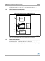
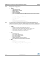
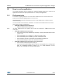
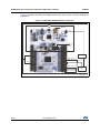
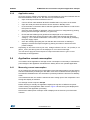
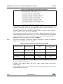
AN4538 Application note Power consumption optimization with STM32F3xx microcontrollers Introduction This application note describes how to optimize the power consumption of an application based on STM32F3xx microcontrollers. Reducing power consumption while performing complex real-time applications presents a major challenge for the recent embedded applications. This application note is splitted in two main parts: • The first part gives an overview of low-power design integrated features and techniques to reduce the power consumption. • The second part describes a use case (a smart motor control application) that highlights the power efficiency of STM32F3xx microcontrollers for the competitive applications of the embedded system market. This application note is provided with the STSW-STM32036 software package that contains an example of STM32F3xx microcontroller low-power application. This application is based on the USART, DMA, timer, comparator, RTC peripherals using STM32F3xx microcontroller low-power modes and features. Table 1. Applicable products and software Type January 2015 Part numbers Microcontrollers STM32F301x6/8, STM32F302x6/8/B/C/D/E, STM32F303x6/8/B/C/D/E, STM32F334xx, STM32F373xx, STM32F318xx, STM32F328xx, STM32F358xx, STM32F378xx, STM32F398xx Software STSW-STM32036 DocID026505 Rev 1 1/25 www.st.com 1 Contents AN4538 Contents 1 STM32F3xx microcontroller low-power overview . . . . . . . . . . . . . . . . . 5 1.1 2 Power supply . . . . . . . . . . . . . . . . . . . . . . . . . . . . . . . . . . . . . . . . . . . . . . . 5 1.1.1 STM32F3xxxx device power supply with an internal regulator . . . . . . . . 5 1.1.2 STM32F3x8xx device power supply . . . . . . . . . . . . . . . . . . . . . . . . . . . . 6 1.1.3 Power supply summary . . . . . . . . . . . . . . . . . . . . . . . . . . . . . . . . . . . . . . 6 1.2 Power mode features . . . . . . . . . . . . . . . . . . . . . . . . . . . . . . . . . . . . . . . . . 7 1.3 Wake up from low-power modes . . . . . . . . . . . . . . . . . . . . . . . . . . . . . . . . 8 1.4 STM32F3xx microcontroller power saving techniques . . . . . . . . . . . . . . . 10 1.4.1 General techniques . . . . . . . . . . . . . . . . . . . . . . . . . . . . . . . . . . . . . . . . 10 1.4.2 Low-power features . . . . . . . . . . . . . . . . . . . . . . . . . . . . . . . . . . . . . . . . 11 STM32F3xx microcontroller low-power application example . . . . . . . 12 2.1 2.2 2.3 2.4 Application description . . . . . . . . . . . . . . . . . . . . . . . . . . . . . . . . . . . . . . . 12 2.1.1 Functional overview . . . . . . . . . . . . . . . . . . . . . . . . . . . . . . . . . . . . . . . . 12 2.1.2 Application modules . . . . . . . . . . . . . . . . . . . . . . . . . . . . . . . . . . . . . . . . 13 2.1.3 State machine . . . . . . . . . . . . . . . . . . . . . . . . . . . . . . . . . . . . . . . . . . . . 15 Software description . . . . . . . . . . . . . . . . . . . . . . . . . . . . . . . . . . . . . . . . . 17 2.2.1 Architecture description . . . . . . . . . . . . . . . . . . . . . . . . . . . . . . . . . . . . . 17 2.2.2 Peripherals configuration . . . . . . . . . . . . . . . . . . . . . . . . . . . . . . . . . . . . 18 How to use the application . . . . . . . . . . . . . . . . . . . . . . . . . . . . . . . . . . . . 19 2.3.1 Environment setup . . . . . . . . . . . . . . . . . . . . . . . . . . . . . . . . . . . . . . . . . 19 2.3.2 Application setup . . . . . . . . . . . . . . . . . . . . . . . . . . . . . . . . . . . . . . . . . . 21 Application current consumption . . . . . . . . . . . . . . . . . . . . . . . . . . . . . . . 21 2.4.1 Measuring current consumption . . . . . . . . . . . . . . . . . . . . . . . . . . . . . . 21 3 Conclusion . . . . . . . . . . . . . . . . . . . . . . . . . . . . . . . . . . . . . . . . . . . . . . . . 23 4 Revision history . . . . . . . . . . . . . . . . . . . . . . . . . . . . . . . . . . . . . . . . . . . 24 2/25 DocID026505 Rev 1 AN4538 List of tables List of tables Table 1. Table 2. Table 3. Table 4. Table 5. Table 6. Applicable products and software . . . . . . . . . . . . . . . . . . . . . . . . . . . . . . . . . . . . . . . . . . . . . 1 STM32F3xxxx device power supply considerations . . . . . . . . . . . . . . . . . . . . . . . . . . . . . . . 7 Wake up from low-power mode sources . . . . . . . . . . . . . . . . . . . . . . . . . . . . . . . . . . . . . . . 9 Wake up from low-power mode timing examples . . . . . . . . . . . . . . . . . . . . . . . . . . . . . . . . . 9 low-power mode data of the measured example . . . . . . . . . . . . . . . . . . . . . . . . . . . . . . . . 22 Document revision history . . . . . . . . . . . . . . . . . . . . . . . . . . . . . . . . . . . . . . . . . . . . . . . . . 24 DocID026505 Rev 1 3/25 3 List of figures AN4538 List of figures Figure 1. Figure 2. Figure 3. Figure 4. Figure 5. Figure 6. Figure 7. Figure 8. 4/25 Power supply overview in STM32F3xxxx devices with an internal regulator . . . . . . . . . . . . 5 Power supply overview in STM32F3x8xx devices . . . . . . . . . . . . . . . . . . . . . . . . . . . . . . . . 6 Application synoptic . . . . . . . . . . . . . . . . . . . . . . . . . . . . . . . . . . . . . . . . . . . . . . . . . . . . . . 12 Application modules and functional interconnections . . . . . . . . . . . . . . . . . . . . . . . . . . . . . 14 Application state machine . . . . . . . . . . . . . . . . . . . . . . . . . . . . . . . . . . . . . . . . . . . . . . . . . . 15 STM32F3xx microcontroller low-power project overview . . . . . . . . . . . . . . . . . . . . . . . . . . 17 NUCLEO-F302R8 hardware connection . . . . . . . . . . . . . . . . . . . . . . . . . . . . . . . . . . . . . . 20 Log time display of the measured example . . . . . . . . . . . . . . . . . . . . . . . . . . . . . . . . . . . . 22 DocID026505 Rev 1 AN4538 1 STM32F3xx microcontroller low-power overview STM32F3xx microcontroller low-power overview STM32F3xx microcontrollers are based on ARM® Cortex®-M4 core running up to 72 MHz with a high number of integrated advanced analog peripherals. They integrate an efficient power supply architecture and various power modes that lead to the power consumption reduction at the application level and simplify the application design. 1.1 Power supply STM32F3xxxx devices have an optimized power supply architecture to combine real-time capabilities, digital signal processing, and low-voltage operations with highly integrated analog peripherals. There are two different power supply architectures, depending on the availability of the internal voltage regulator in the STM32F3xx microcontrollers: 1.1.1 STM32F3xxxx device power supply with an internal regulator The embedded voltage regulator is used to supply the internal 1.8 V digital power domain that contains the core, the memories and the digital peripherals as described in Figure 1. Figure 1. Power supply overview in STM32F3xxxx devices with an internal regulator 9''$GRPDLQ 966$ 9 ''$ $'FRQYHUWHU '$FRQYHUWHU 7HPSVHQVRU 5HVHWEORFN 3// 5&V 23$03 &RPSDUDWRUV 9''GRPDLQ 9GRPDLQ ,2ULQJ 966 9'' 6WDQGE\FLUFXLWU\ :DNHXSORJLF ,:'* &RUH 0HPRULHV 'LJLWDO SHULSKHUDOV 9ROWDJHUHJXODWRU /RZYROWDJHGHWHFWRU 57&GRPDLQ 9%$7 /6(FU\VWDO.RVF %.3UHJLVWHUV 5&&%'&5UHJLVWHU 57& 069 DocID026505 Rev 1 5/25 24 STM32F3xx microcontroller low-power overview AN4538 STM32F3xx microcontrollers, with embedded voltage regulator, require a 2.0 V - 3.6 V operating supply voltage (VDD) and a 2.0 V - 3.6 V analog supply voltage (VDDA). 1.1.2 STM32F3x8xx device power supply These devices do not contain a voltage regulator. VDD directly supplies the regulator output as described in Figure 2. Figure 2. Power supply overview in STM32F3x8xx devices 9''$GRPDLQ 9''$ 966$ $'FRQYHUWHU '$FRQYHUWHU 7HPSVHQVRU 5HVHWEORFN 3// 9''GRPDLQ 9'' 966 1325 9%$7 9'',2 ,2ULQJ :DNHXSORJLF ,:'* 9GRPDLQ &RUH 0HPRULHV 'LJLWDO SHULSKHUDOV %DFNXSGRPDLQ /6(FU\VWDO.RVF %.3UHJLVWHUV 5&&%'&5UHJLVWHU 57& 06Y9 The STM32F3xx microcontrollers require a 1.8 V +/- 8% operating voltage supply (VDD) and 1.65 V - 3.6 V analog voltage supply (VDDA). Standby mode is not supported. 1.1.3 Power supply summary In both power supply architectures, the real-time clock (RTC) and the backup registers can be powered from the VBAT voltage when the main VDD supply is off. Table 2 summarizes the power supply ranges in both architectures and gives supply conditions to be taken into account. 6/25 DocID026505 Rev 1 AN4538 STM32F3xx microcontroller low-power overview Table 2. STM32F3xxxx device power supply considerations Internal regulator status Voltage regulator ON VDDA VDD From 2V to 3.6V From 2V to 3.6V Power domain considerations • • • Voltage regulator OFF 1.8V ± 8% From 1.65V to 3.6V VDDA ≥ VDD VDDA ≥ 2.4V when DAC and OPAMP are used. VDDA ≥ 1.8V • when ADC is used. • No considerations POR, PDR and PVD features are not available. Standby mode is not available. Note: For more details about the power supply, you can refer to the reference manuals RM00313, RM0316, RM0364, RM0365, RM0366 and to the relevant datasheets available from the STMicroelectronics web site. 1.2 Power mode features By default, after power-on or system reset, the STM32F3xx microcontrollers are in Run mode. This is a fully active mode that consumes much power even when performing minor tasks. Highly optimized low-power modes are integrated to save power when the CPU does not need to be kept running, thus allowing to achieve the best compromise between a lowpower consumption, a short startup time and available wakeup sources in the application design. This part describes the different low-power modes available in STM32F3xxxx devices and the related features. STM32F3xxxx devices feature four main low-power modes: • • Sleep mode: – Only the CPU clock is stopped. – The Cortex®-M4 clock is stopped and the peripherals are kept running. The current consumption increases with the clock frequency. As in a Run mode, the user needs to know the system clock configuration rules. Stop mode – The lowest power consumption while all the SRAM and registers are kept. – PLL, HSI, HSE are disabled. – All clocks in 1.8 V domain are switched off. – Voltage regulator is working in normal mode or low-power modes. Stop mode achieves the lowest power consumption while retaining the content of SRAM and registers. All clocks in the 1.8 V domain are stopped, the PLL, the HSI and the HSE are disabled. The voltage regulator can also be put either in normal or in low-power modes (not available when internal regulator is off). DocID026505 Rev 1 7/25 24 STM32F3xx microcontroller low-power overview • AN4538 Standby mode – The lowest power consumption. – The 1.8V domain is powered off (regulator is disabled). – SRAM and register contents are lost except in the backup domain. The Cortex®-M4 core is stopped and the clocks are switched off. The voltage regulator is disabled and the 1.8 V domain is powered off. SRAM and register contents are lost except for the registers in the Backup domain (RTC registers, RTC backup register and backup SRAM), and Standby circuitry. Note: Standby mode is not available in devices where the internal regulator is OFF. • Vbat mode: – The main digital supply (VDD) is turned off. – The circuit is supplied through VBAT pin which should be connected to an external supply voltage (a battery or any other source). This mode is used only when the main digital supply (VDD) is turned off and the VBAT pin is connected to an external supply voltage. The VBAT pin powers the Backup domain (RTC registers, RTC backup register and backup SRAM). Note: For a further description of these low-power mode features and low-power technology of STM32F3xxxx devices, you can refer to the RM00313, RM0316, RM0364, RM0365, RM0366 reference manuals and the relevant datasheets available from the STMicroelectronics web site. 1.3 Wake up from low-power modes STM32F3xxxx devices integrate many wakeup sources to offer a flexible power management in a low-power application development and to simplify the application design. Many I/O pins allow to use these different wakeup sources. Table 3 describes the different wakeup sources and pins that can be available in STM32F3xxxx devices. 8/25 DocID026505 Rev 1 AN4538 STM32F3xx microcontroller low-power overview Table 3. Wake up from low-power mode sources Mode name Entry Wakeup sources WFI Any interrupt Wakeup pins Wakeup event Sleep Comparator can wake up from Sleep (up to WFE 7 EXTI lines in STM32F303xB/C/D/E, STM32F358xx and STM32F398xx) All I/O Any EXTI line (configured in the EXTI registers, internal and external lines) PDDS, LPDS bits + SLEEPDEEP bit + Stop WFI or WFE EXTI lines connected internally to: (1) • U(S)ART • Comparator • I2C • CEC (2) PDDS bit + Standby WKUPx pins (x = 1, 2, 3), RTC alarm, RTC SLEEPDEEP bit + tamper event, external reset in NRST pin, IWDG reset WFI or WFE PA0 PC13 PE6 (3) 1. For EXTI lines connected internally to these peripherals refer to EXTI lines mapping section in the reference manuals. 2. CEC Available only in STM32F37xxx. 3. PE6 works as wakeup pin only in STM32F303/302xB/C/D/E. The wakeup time from low-power modes contributes a lot in the power optimization and the application flexibility. A trade-off has to be done between the low-power modes consumption and the correspondent wakeup time. Table 4 gives examples of wake up from low-power mode timing in STM32F3xx microcontrollers. Table 4. Wake up from low-power mode timing examples Parameter Typ, VDD=VDDA=3,3 V Condition STM32F302x6/8 Wake up from Sleep Wake up from Stop Wake up from Standby Unit STM32F303xB/C STM32F373xx CPU clock cycles 6 Regulator in Run mode 3.8 3.6 3.6 Regulator in lowpower modes 5.7 5.4 5.4 LSI and IWDG OFF 53.1 51.7 42.7 DocID026505 Rev 1 µs 9/25 24 STM32F3xx microcontroller low-power overview 1.4 STM32F3xx microcontroller power saving techniques 1.4.1 General techniques AN4538 This section gives a brief description of the main power-saving features that contribute a lot reducing the current consumption and reaching an optimal trade-off between the performance processing and the power efficiency. • System clock configuration Several prescalers are used to configure the AHB frequency, the high-speed APB (APB2) and the low-speed APB (APB1) domains. In Run mode, the speed of the system clocks can be reduced by programming the registers prescalers to the highest values in order to provide just the needed clocks to peripherals and avoid the overclocking that causes a consumption penalty. The power consumption can be further lowered by gating clocks to the APBx and AHBx peripherals when they are not in use. • I/O configuration To avoid extra I/O currents, all unused pins should be configured as analog inputs, in this mode the schmitt trigger input is disabled, providing zero consumption for each I/O pin. For the output, it is recommended to configure the I/O speed frequency at the lowest possible speed. The user has to avoid the pull-up and pull-down activation if they are not used and no-pull up/down configuration is recommended. The user has to also disable the MCO pin of the clock output if not used. • Using direct memory access (DMA) STM32F3xxxx device peripherals can be accessed through DMA. This feature is not just useful to improve the performance, it can also be used to reduce the power consumption. The CPU must be kept running to avoid overflow on peripherals featuring only one buffer register. However, with DMA, the CPU can go to Sleep mode until the completion of DMA transfer. This allows the device to consume less average current over the life of the application. • Using low-power modes Power mode switching in the application processing reduces the overall average consumption by keeping the device as much as possible in low-power modes. The best power management approach consists of switching between different power modes, taking into account of the application requirements in terms of power consumption, wakeup sources/time and the peripherals simultaneously. • Peripherals clock gating The more peripheral blocks active simultaneously the highest the power consumption. Substantial power saving can be achieved by gating the clocks of the peripherals that are not in use. • Using peripheral low-power features STM32F3xxxx devices have peripherals with particular power features that allow to design and develop low-power applications while maintaining a high flexibility and an easy interaction with the external world. For example, the devices can wake up from low-power modes using USART, comparator, I2C and CEC. 10/25 DocID026505 Rev 1 AN4538 1.4.2 STM32F3xx microcontroller low-power overview Low-power features Some STM32F3xxxx peripherals have low-power features which facilitate the use of lowpower modes while maintaining a high processing capability. The availability of these features differs between the STM32F3xx microcontrollers. • COMP The STM32F3xxxx comparators work independently from the PCLK2 clock. Thanks to this clock, the comparators can even operate in Stop mode. Each comparator has its own EXTI line and can generate either interrupts or events, which can wake up the device from both Sleep and Stop modes. The outputs can be connected to an I/O or to multiple timer inputs in order to trigger control and monitor analog signals during Sleep mode. The comparator power consumption versus speed can be adjusted to have the optimum trade-off for a given application (This feature is available only in the STM32F303/302xB/C, STM32F358xx, STM32F373xx and STM32F378xx devices.). • U(S)ART All U(S)ART interfaces can be served by the DMA controller during Sleep mode. USART supports a dual clock domain which allows the functionality and wake up from Stop mode. USART can wake up from Stop mode via either address match, start bit or by RXNE when its clock source is HSI or LSE. Such feature facilitates the design and development of the application while maintaining the power efficiency. Note that the user can put the IrDA SIR ENDEC in low-power mode to save more power. • I2C DMA can be used to reduce CPU overload and thus the power consumption. The I2C is clocked by an independent clock source which allows the I2C to operate independently from the PCLK frequency. When the I2C clock source is the HSI, the I2C can wake up from Stop mode on address match. • CEC Consumer Electronics Control protocol can operate at low speeds with a minimum processing and memory overhead. It has a clock domain independent from the CPU clock, allowing to wake up the MCU from Stop mode on data reception. HDMI_CEC controller is embedded only in STM32F37xxx devices. • ADC The STM32F3xxxx devices (except for STM32F373/378xx devices) embed a lowpower ADC which consumption is proportional to the speed. The lowest consumption is got with the lowest speed. This ADC has two clock sources derived from AHB and PLLCLK clocks. Consequently, the max speed 5MSPS can be reached even with a slow AHB bus frequency. In this case, ADC auto-delayed feature is available in order to avoid ADC overruns. DocID026505 Rev 1 11/25 24 STM32F3xx microcontroller low-power application example 2 AN4538 STM32F3xx microcontroller low-power application example This section describes a real use case with STM32F3xx microcontrollers and focuses on the power saving techniques used to reduce the consumption of this application. 2.1 Application description The application is designed as a smart motor monitor and control with the integration of different low-power modes and features. It communicates messages to the user about the different application steps and the log time profile. 2.1.1 Functional overview The application is designed using the NUCLEO-F302R8 board based on a STM32F302x8 device. The main features of this application are: • The use of multiple peripherals: USART, DMA, Timer, COMP, DAC, RTC • The use of multiple low-power modes: Sleep, Stop, Standby • The real-time log data: RTC calendar (LSE) The following figure gives an overview of the application ecosystem. Figure 3. Application synoptic The application starts when the NUCLEO-F302R8 is powered on. Once the user has pushed the button or the defined RTC time has elapsed, the user has to choose the 12/25 DocID026505 Rev 1 AN4538 STM32F3xx microcontroller low-power application example reference voltage which will be used by the comparator to control external analog signal (motor current threshold). Once the selection is done, the application starts driving the motor by a PWM signal generated using timer1. Simultaneously, the comparator controls an input analog signal (motor current). When this signal reaches the selected reference voltage, the generation of PWM signal is stopped. The application embeds several power modes that allow optimizing the whole application power consumption. The RTC timer is enabled during the whole application to save time of each state. The application communicates messages to the user about the main application transitions. The log time of different states can be displayed, if this feature has been enabled by the user. This log time profile gives the opportunity to the user to calculate easily the application power budget. 2.1.2 Application modules The application is based on a NUCLEO-F302R8, connected to a PC via USB cable. The main STM32F302x8 peripherals used by this application are: • USART1: used to send and receive data via virtual comport and to wake up the CPU from Stop mode. • DMA: used with USART for data transfer from device to PC • Timer 1: used to generate PWM signal. • Comparator 2: used to stop PWM generation and wake up the CPU from Sleep mode when the non inverting input voltage exceeds the reference voltage. • RTC: used to run a calendar in the whole application and to wake up the CPU from standby after the pre-defined time has elapsed. Figure 4 summarizes the different modules of the application and the relevant functional interconnections. DocID026505 Rev 1 13/25 24 STM32F3xx microcontroller low-power application example AN4538 Figure 4. Application modules and functional interconnections 2FUHI&OHDU 6WRS3:0 :DNHXS IURPVOHHS &38 &RUWH[0 7,0(5 2&& 3:0VLJQDO ([WHUQDODQDORJVLJQDO &203 3$ 3$ 9UHILQW '$&B287 :DNHXS IURPVWDQGE\ 3$ :DNHXS IURPVWDQGE\ 3$ 7[ 3$ 5[ 57& &DOHQGDU :DNHXS :DNHXS IURPVWRS 86$57 '0$ 0HPRU\ 06Y9 There are four different wakeup sources: 14/25 • PA0: wake up from Standby mode • USART wakeup source: wake up from Stop mode • Comparator: wake up from Sleep mode. • RTC: wake up from Standby mode. DocID026505 Rev 1 AN4538 State machine The state machine provided in Figure 5 describes the application states and transitions. Figure 5. Application state machine 5(6(7 581 57& 6OHHS ' :DNHXSBIODJ .3 8 581 3$ : 3$ : 8 .3 H HW SO RU 5 7& RP F HU : 8 /3 I QV WUD $ 0 '0$ WUDQVIHU RQJRLQJ 581 581 6WDQGE\ &203B:8.3 3$:8.3 RU 57&:8.3 6OHHS 6OHHS &203B:8.3 86$57B:8.3BIODJ 581 ' 0 F $W RP UD SO QVI HW HU H 6$ 5 : 8 .3 6723 8 2.1.3 STM32F3xx microcontroller low-power application example '0$WUDQVIHU RQJRLQJ 581 06Y9 DocID026505 Rev 1 15/25 24 STM32F3xx microcontroller low-power application example • AN4538 State machine Initially, the device is in Standby mode. First, the user pushes the user-button to wake up the device from standby. If the user does not push the button, the device will wake up via RTC after a pre-defined period (20 s by default). Then, the device sends data, via the virtual comport (see Sleep1 state description). Once the transfer is completed, the CPU enters Stop mode. The device remains in Stop mode until the user pushes a keyboard button to transfer a number from 1 to 4. It will simultaneously wake up the device via USART, select the desired configuration of the comparator inverting input (Vrefint or DAC1_OUT1) and the RTC display (yes or no). Then, the STM32F302x8 device enters Sleep mode. In this mode, timer 1 generates the PWM signal and the comparator is active to detect in real time when the non inverting input voltage exceeds the chosen reference voltage (inverting input). In this case, the comparator generates an interruption that wakes up the device from Sleep mode and stops PWM generation via the internal signal OCref_clr. After that, Sleep mode is entered again to send, via DMA, the data about previous state and the log time of all states (if already enabled). When the DMA transfer is completed, the device enters Standby mode. • 16/25 States: – Run1: When the device is powered on, it configures the system clock and the RTC calendar and wakeup sources. – Standby: After power-on, the device enters Standby mode after the configuration in Run1 is configured and remains in Standby mode until it is woken up (wakeup pin or RTC). – Run2: After waking up from Standby mode, configures USART, DMA to be ready for transfer and read time. – Sleep1: Sends a message to the user via DMA about the possible configurations to select. Once the transfer is completed, the device wakes up from Sleep1. – Run3: Configures the USART wakeup source to be used in Stop mode, then reads the time. – Stop: Remains in Stop mode until a USART data is received to wake up the device. – Run4: Configures and starts COMP2, TIM1 and DAC1 if used, then reads the time. – Sleep2: Sends a message to the user via DMA. TIM1 generates a PWM signal. The comparator is active to compare the injected analog signal to Vrefint or DAC1_OUT1. When a comparator interruption occurs, it wakes up the device from Sleep mode and stops the PWM generation via OCref_clr. – Run5: Disables TIM1, COMP2 and DAC if used, then reads the time, prepares to display the log time profile if it is selected. – Sleep3: Sends a message including the log time profile. Once the transfer is completed, the device wakes up from Sleep3 mode. – Run6: Reads the time and saves it in the backup domain. Reconfigures the RTC before entering again Standby mode to start a new round. DocID026505 Rev 1 AN4538 STM32F3xx microcontroller low-power application example 2.2 Software description 2.2.1 Architecture description This application uses the STM32F3xx HAL library and contains the following source files: • Main.c: contains the needed functions that perform the application state machine • STM32F3xx_it.c: contains the interrupt handlers for the application • STM32F3xx_hal_msp.c: contains the needed hardware configuration of the different peripherals used by the application. Figure 6. STM32F3xx microcontroller low-power project overview 'ULYHUV IROGHU %63 VXEIROGHU &06,6 VXEIROGHU 670)[[B+$/B'ULYHU VXEIROGHU 3URMHFW IROGHUV (:$50DQG0'. $50SURMHFWV 8VHUKHDGHUILOHV 8VHUVRXUFHILOHV 5HDGPHILOH 06Y9 DocID026505 Rev 1 17/25 24 STM32F3xx microcontroller low-power application example 2.2.2 Peripherals configuration • • Note: Timer1 – TIM1_output: pin PA8. – APB2 Prescaler = 1 (8 MHz) – Period = 1/20 KHz – Pulse = 50% of Period – OCref_clr is enabled to disable the PWM generation when high level is detected. UART1 – USART1_Tx (PA9), USART1_Rx (PA10) – Baud Rate: 115200 bps – Word length: 8 bits – Stop bits: 1 – Hardware flow control and parity: none – UART wakeup from Stop mode: EXTI line 25 The virtual comport is connected to the USART2 in the NUCLEO-F302R8 board. Use USART1 in the software to support the «USART wakeup from stop feature». USART2 pins should be connected to USAR1 pins. The virtual comport software should be downloaded. • COMP2 – • • 18/25 AN4538 COMP2 non inverting input (COMP2_INP): pin PA7 – COMP2 inverting input (COMP2_INM): VREFINT or DAC1_OUT1 – COMP outputs: TIM1_OCref_clr / COMP_OUT: pin PA12 – COMP wakeup from Sleep mode: EXTI line 22 RTC – Clock source: LSE – RTC_ASYNCH_PREDIV: 0x7F – RTC_SYNCH_PREDIV: 0x00FF – RTC_OUTPUT: disable – Calendar: format12, hour, minute, second – RTC wakeup: EXTI line 20 to wake up from standby. DAC – Channel: 1 – Data alignment: 12 bit data alignment. – Data: 2500 (by default), it can be modified by the user. DocID026505 Rev 1 AN4538 2.3 STM32F3xx microcontroller low-power application example How to use the application This section describes how to prepare the NUCLEO-F302R8 board to be used for the application as well as the steps performed to run correctly the application. 2.3.1 Environment setup First read the «getting started» of the NUCLEO-F302R8 board user manual UM1724 to prepare the NUCLEO-F302R8 board for a correct use. The version of the NUCLEO-F302R8 board to be used is MB1136-C 02 (with on-board 32kHz oscillator). The user needs to know about the hardware connections and modifications that must be done before running the application. • NUCLEO-F302R8 board modifications – Note: SB62 and SB63 solder-bridges ON For more details about LSE please refer to the user manual of STM32 Nucleo board «UM1724». • • NUCLEO-F302R8 board connections – Connect the JP5 jumper between pin 2 and pin 3 (U5V) and make sure the JP1 jumper is off. – Connect USART2_Tx to USART1_Tx: PA2 connected to PA9 – Connect USART2_Rx to USART1_Rx: PA3 connected to PA10 – Connect PA0 to a button connected to VDD and GND via pull-down. – Connect the Idd jumper JP6 to the multimeter terminals. NUCLEO-F302R8 board connections to the instruments – Connect the oscilloscope probe to PA8 pin. – Connect the DC power supply output to pin PA7 and regulate it to a voltage lower than the comparator reference voltage (1.2 V if Vrefint selected or 2V if DAC1_OU1 selected). Turn off the power supply. DocID026505 Rev 1 19/25 24 STM32F3xx microcontroller low-power application example AN4538 Figure 7 describes the NUCLEO-F302R8 connections that must be set before starting the application. Figure 7. NUCLEO-F302R8 hardware connection $ 86%FDEOH *1' -3RQ SRVLWLRQ 89 2VFLOORVFRSH 9GG 3$86$57B7; 3$7,0B&+ 3$&203B,13 3$ 3$86$57B5; 3$86$57B7; '&3RZHU VXSSO\ 3$86$57B5; 06Y9 20/25 DocID026505 Rev 1 AN4538 2.3.2 STM32F3xx microcontroller low-power application example Application setup Once the previous software and hardware recommendations have been followed and the NUCLEO-F302R8 is ready to use, the user has to proceed as follow: Note: • Open a serial port terminal interface in the PC. • Connect ST-link cable between NUCLEO-F302R8 and PC to power-on the board. • Open the serial port terminal while the device remains in Standby mode. • Push the button connected to PA0 to start the application state machine or wait for the RTC period to elapse. • Once the menu message is displayed, select one of the four configuration by pushing the key and send the right character (1-4).(see note) • Ensure that the PWM signal is generated and displayed on the oscilloscope. • Turn on the DC power supply and apply a DC voltage that exceeds the reference voltage (≥ 1.2 V if Vrefint is selected or ≥ 2V if DAC1_OUT1 is selected) by modifying the power supply output. • Once the message prompting the user that the device will return to standby is displayed, execute the sequence again by pushing the button or wait for the RTC period to elapse. Depending on the choice done by the user, Voltage reference can be 1.2V (Vrefint) or 2V (DAC1_OUT1) and the log time can be displayed or not in the last message. The user has to apply the same sequence of steps described above to get a correct functionality of the application. 2.4 Application current consumption The measure of the application's average current consumption is necessary to estimate the power budget of the application and deduce the battery life for such portable application. 2.4.1 Measuring current consumption As an example, the average current consumption of the first state machine cycle processing has been measured by activating the ’Min Max’ mode of the multimeter before powering on the NUCLEO-F302R8 board. The hold button is pushed just after the first return to Standby mode. In this measured case, the Vrefint is selected as the inverting input of the comparator 2 and the log time display is activated. The average current is equal to 480 µA. Before returning to standby, the application displays the log time of different low-power modes existing in the application state machine. Figure 8 shows the log time displayed for the first time of the application processing. Note that the wakeup time of Sleep3 mode is displayed in the second cycle of the state machine. DocID026505 Rev 1 21/25 24 STM32F3xx microcontroller low-power application example AN4538 Figure 8. Log time display of the measured example The time spent in each mode and the corresponding current consumption helps us to calculate an estimated value of the whole application average current consumption. The formula of the average current consumption is as follows: I average = (IRUNx * TimeRUNx + Istandby * Timestandby + Isleep1 * Timesleep1 + Istop * Timestop + Isleep2 * Timesleep2 + Isleep3 * Timesleep3 ) / Total Time Table 5 gives the time and the current consumption in different low-power modes of the measured example. For Runx modes (x=1, 2, 3, 4, 5, 6), we assume that they are negligible versus low-power modes in term of processing periods in a such low-power application. Total time = wake up from Sleep3 mode time = 42488 ms Note: The current consumption of low-power modes is measured by holding the multimeter display in each measured state of the application. Table 5. low-power mode data of the measured example Active peripherals Execution periods (ms) Average measured current consumption (µA) Standby mode RTC (LSE, Backup domain) 20015 4.3 Sleep1 mode RTC, USART1/DMA1 82 2010 RTC, USART1 12957 24.3 Sleep 2 mode RTC, USART1/DMA1, COMP2, TIM1 9336 2080 Sleep3 mode RTC, USART1/DMA1 90 2040 Low-power modes Stop mode Applying the average formula gives: I average = [(4.3 * 20015) + (2010 * 82) + (24.3 * 12957) + (2080 * 9336) + (2040 * 90)] / 42488 = 475 µA So the calculation gives us a good average current consumption compared to the measured one with almost only 1% error. 22/25 DocID026505 Rev 1 AN4538 3 Conclusion Conclusion This application note illustrates the low-power features integrated into the STM32F3xx microcontrollers. They ensure the best trade-off between the power efficiency and high performance. This document provides an overview on these power features and describes how to correctly configure the different power modes through a real use case to minimize the power current consumption. DocID026505 Rev 1 23/25 24 Revision history 4 AN4538 Revision history Table 6. Document revision history 24/25 Date Revision 06-Jan-2015 1 Changes initial release. DocID026505 Rev 1 AN4538 IMPORTANT NOTICE – PLEASE READ CAREFULLY STMicroelectronics NV and its subsidiaries (“ST”) reserve the right to make changes, corrections, enhancements, modifications, and improvements to ST products and/or to this document at any time without notice. Purchasers should obtain the latest relevant information on ST products before placing orders. ST products are sold pursuant to ST’s terms and conditions of sale in place at the time of order acknowledgement. Purchasers are solely responsible for the choice, selection, and use of ST products and ST assumes no liability for application assistance or the design of Purchasers’ products. No license, express or implied, to any intellectual property right is granted by ST herein. Resale of ST products with provisions different from the information set forth herein shall void any warranty granted by ST for such product. ST and the ST logo are trademarks of ST. All other product or service names are the property of their respective owners. Information in this document supersedes and replaces information previously supplied in any prior versions of this document. © 2015 STMicroelectronics – All rights reserved DocID026505 Rev 1 25/25 25