1
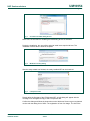
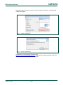
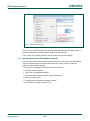
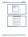
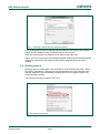
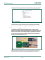
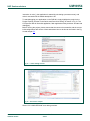
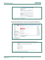
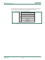
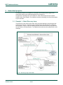
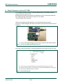
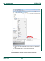
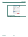
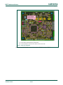
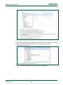
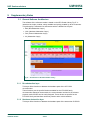
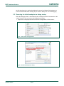
UM10954 PN5180 SW Quick start guide 1.0 — 26 November 2015 345810 User manual COMPANY PUBLIC Document information Info Content Keywords PN5180, PN5180 SW design, PNEV5180B Abstract This user manual is related to the installation procedures of the PN5180 Evaluation board, which are related to the installation of the SW sample projects as well as the re-installation of the original LPC firmware to run the NFC Cockpit. It describes the steps to be done to become acquainted with the demo reader especially for SW development. UM10954 NXP Semiconductors PN5180 SW Quick start guide Revision history Rev Date Description 1.0 Initial version 20151126 Contact information For more information, please visit: http://www.nxp.com For sales office addresses, please send an email to: [email protected] UM10954 User manual COMPANY PUBLIC All information provided in this document is subject to legal disclaimers. 1.0 — 26 November 2015 345810 © NXP B.V. 2015. All rights reserved. 2 of 31 UM10954 NXP Semiconductors PN5180 SW Quick start guide 1. Introduction This document is the continuation of the “AN11744 - PN5180 Quick start guide” and describes the installation procedures of the SW development environment and handling SW example projects using the NFC Reader Library prepared for the PN5180 evaluation board. It also describes how to re-install the original LPC firmware binary to use the NFC Cockpit again. Projects used and explained in this documentation are: Table 1. Example projects Example projects delivered with the NFC Reader Library Example Description Example 1 – Basic Discovery Loop Explains how to poll for different technologies (Tag, P2P, HCE), detect and report them. Default configuration parameters are used. Example 2 – Explains how to poll for different technologies (Tag, P2P, HCE), Advanced Discovery Loop detect and report them. All configuration parameters are used and explained. UM10954 User manual COMPANY PUBLIC Example 4 – MIFARE Classic Explains the usage of standard MIFARE commands. Example 5 – ISO15693 Explains the usage of this technology and provides an overview about the most common commands. Example 6 – EMVCo Loopback Application used for EMVCo Level 1 PCD certification. Example 7 – EMVCo Polling Explains polling for EMVCo payment cards. Example 9 – NTAG-I2C Explains NTAG-I2C specific commands. ICODE ILT/SLI Extensively explains the communication with ICODE ILT and ICODE SLI tags. This example is provided in a separate package. All information provided in this document is subject to legal disclaimers. 1.0 — 26 November 2015 345810 © NXP B.V. 2015. All rights reserved. 3 of 31 UM10954 NXP Semiconductors PN5180 SW Quick start guide 2. Managing the PN5180 SW projects with LPCXpresso IDE The PN5180 SW projects are delivered in a zip package and can be extracted, edited, compiled and linked with LPCXpresso IDE. The LPCXpresso IDE is a low-cost highly integrated software development environment for NXP's LPC microcontrollers and includes all the tools necessary to develop highquality software solutions in a timely and cost effective fashion. LPCXpresso IDE is based on Eclipse and has many enhancements to simplify development with NXP LPC microcontrollers. It also features the industry-standard GNU tool chain, with a choice of a proprietary optimized C library or the standard “Newlib” library. The LPCXpresso IDE can build an executable of any size with full code optimization. Designed for simplicity and ease of use, the LPCXpresso IDE provides software engineers a quick and easy way to develop their applications. This tool can freely be downloaded from the LPCXpresso website [1]. Before one can download the software, it is necessary to create an account. Creating an account is absolutely free. 2.1 Development environment To use PN5180 prepared software package all components listed in the Table 2 are required. Table 2. Item Development Environment Version Description PN5180EV5180B 1.0 or higher PN5180 Customer Evaluation board (hardware) LPC-Link 2 1.0 Standalone debug adaptor (hardware) LPCXpresso IDE 7.9.0 or higher Development IDE (PC software) 2.2 Installation procedure of the LPCXpresso IDE The LPCXpresso IDE is installed into a single directory, of your choice. Unlike many software packages, the LPCXpresso IDE does not install or use any keys in the Windows Registry, or use or modify any environment variables (including PATH), resulting in a very clean installation that does not interfere with anything else on your PC. Should you wish to use the command-line tools, a command file is provided to set up the path for the local command window. Multiple versions can be installed simultaneously without any issues. The installation starts after double-clicking the installer file. UM10954 User manual COMPANY PUBLIC All information provided in this document is subject to legal disclaimers. 1.0 — 26 November 2015 345810 © NXP B.V. 2015. All rights reserved. 4 of 31 UM10954 NXP Semiconductors PN5180 SW Quick start guide Fig 1. Check box for NXP debug drivers Make sure, the checkbox for installing the NXP debug drivers is activated. During the installation, the user will be asked to install some required drivers. The installation of these drivers shall be accepted. Fig 2. Windows security dialog After the setup wizard has finished, the newly installed IDE can be launched. Fig 3. LPCXpresso IDE Directly after the first start of the LPCXpresso IDE, an info dialog will appear with the message of an unregistered copy of the LPCXpresso IDE. Confirm the dialog and follow the instructions on the Welcome Screen to get a registered version with the debug limit of 256k. The registration is free of a charge. The link to the UM10954 User manual COMPANY PUBLIC All information provided in this document is subject to legal disclaimers. 1.0 — 26 November 2015 345810 © NXP B.V. 2015. All rights reserved. 5 of 31 UM10954 NXP Semiconductors PN5180 SW Quick start guide registration page is shown in the menu, Help Activate LPCXpresso Create Serial number and register. Fig 4. Product activation (1) Fig 5. Product activation (2) In case that you do not have an account on the http://www.nxp.com/redirect/lpcware.com, simply sign up to get an activation code. The code will be sent to the provided e-mail address. UM10954 User manual COMPANY PUBLIC All information provided in this document is subject to legal disclaimers. 1.0 — 26 November 2015 345810 © NXP B.V. 2015. All rights reserved. 6 of 31 UM10954 NXP Semiconductors PN5180 SW Quick start guide Fig 6. Product activation (3) Once you receive the activation code open the activation window by pointing to Help Activate LPCXpresso Enter Activation code, and enter the code. The success of the product activation will be confirmed by an info dialogue. 2.3 Importing provided SW example projects The use of quick start panel provides rapid access to the most commonly used features of the LPCXpresso IDE. Quick start panel allows easy import projects, create new projects, build and debug projects. The sequence of installing the software projects is indicated: • Start the LPCXpresso IDE. • Open new or dedicated workspace • Select the option “Import project(s)” (see picture below). • Browse the zip archive. • LPCXpresso IDE unzips the software package. • The software package is ready for use. UM10954 User manual COMPANY PUBLIC All information provided in this document is subject to legal disclaimers. 1.0 — 26 November 2015 345810 © NXP B.V. 2015. All rights reserved. 7 of 31 UM10954 NXP Semiconductors PN5180 SW Quick start guide Fig 7. Importing a project into the LPCXpresso IDE (1) In the Quick Panel on the left hand side, choose “Import projects(s)”. Fig 8. Importing a project into the LPCXpresso IDE (2) Browse the desired package and click “Next”. UM10954 User manual COMPANY PUBLIC All information provided in this document is subject to legal disclaimers. 1.0 — 26 November 2015 345810 © NXP B.V. 2015. All rights reserved. 8 of 31 UM10954 NXP Semiconductors PN5180 SW Quick start guide Fig 9. Importing a project into the LPCXpresso IDE (3) For a working demo project you need to import at least four sub projects. One example project, the NFC Reader Library, FreeRTOS and one MCU project. When the import process has finished one can start browsing the code. Before one can run the project, the LPCXpresso board containing the PN5180 Blueboard needs to be connected to the computer. Wait until the adequate drivers have been installed. 2.4 Building projects Building projects in a workspace is a simple case of using the Quick start Panel - ‘Build all projects’. Alternatively a single project can be selected in the “Project Explorer View” and built separately. Note that building a single project may also trigger a build of any associated library projects. The project can be built as shown in the Fig 10. Fig 10. Building the project UM10954 User manual COMPANY PUBLIC All information provided in this document is subject to legal disclaimers. 1.0 — 26 November 2015 345810 © NXP B.V. 2015. All rights reserved. 9 of 31 UM10954 NXP Semiconductors PN5180 SW Quick start guide As a part of the build output, the binary for the “User Flash” file is created. This binary file can be later also used to update PN5180 User Flash via USB mass storage interface. (1) Fig 11. Figure title here The project settings, compiler and link flags can be changed in the project properties dialog. To open the project properties dialog, select appropriate project in the “Project Explorer View” and click “Edit ‘selected-project’ project settings”. 2.5 Running and debugging a project This description shows how to run the “NfcrdlibEx6_EMVCo_Loopback” example application for the PN5180 evaluation development board. The same basic principles will apply for all other examples. In cases where example will need additional configuration this will be detailed described in the example description. First of all you need to ensure that your PN5180 evaluation board is connected to the computer via LPC-LINK2, as shown in Fig 12. LPC-LINK2 SWD-connector Fig 12. PNEV5180B with LPC-Link2 When debug is started, the program is automatically downloaded to the target and it´s programmed to the LPC1769 flash memory; a default breakpoint is set on the first UM10954 User manual COMPANY PUBLIC All information provided in this document is subject to legal disclaimers. 1.0 — 26 November 2015 345810 © NXP B.V. 2015. All rights reserved. 10 of 31 UM10954 NXP Semiconductors PN5180 SW Quick start guide instruction in main (), the application is started (by simulating a processor reset), and code is executed until the default breakpoint is hit. To start debugging your application on the PN5180, simply highlight the project in the Project Explorer and then in the Quick start Panel click Debug, as shown in Fig 13. The LPCXpresso IDE will first build application, flash application binary and then will start with debugging. Before running the project, please ensure that the correct microcontroller and the correct build configurations are chosen. Information about how to do this can be found in the Fig 29 and chapter 5.3. Fig 13. Launch debug session Fig 14. Successful compile Select “LPC-LINK2 REDLINK” as a debug emulator. UM10954 User manual COMPANY PUBLIC All information provided in this document is subject to legal disclaimers. 1.0 — 26 November 2015 345810 © NXP B.V. 2015. All rights reserved. 11 of 31 UM10954 NXP Semiconductors PN5180 SW Quick start guide Fig 15. Select the launch configuration After successful software upload, the execution of the project starts immediately, but might halt at the initial breakpoint. To resume execution, please click the resume button. Fig 16. Debug project In the console window application debug outputs of the execution can be seen. Fig 17. Application printouts in Console window UM10954 User manual COMPANY PUBLIC All information provided in this document is subject to legal disclaimers. 1.0 — 26 November 2015 345810 © NXP B.V. 2015. All rights reserved. 12 of 31 UM10954 NXP Semiconductors PN5180 SW Quick start guide After the execution has reached the end of the main function please click the Terminate button to stop the execution. Otherwise rerun of the project will be possible. Buttons in the debug toolbar provide next functionalities: Run the program. Step over C/C++ line. Step into a function. Stop the debugger. Pause execution of the running program. Instruction stepping mode (disassembly). Fig 18. Debug Buttons UM10954 User manual COMPANY PUBLIC All information provided in this document is subject to legal disclaimers. 1.0 — 26 November 2015 345810 © NXP B.V. 2015. All rights reserved. 13 of 31 UM10954 NXP Semiconductors PN5180 SW Quick start guide 3. Associated projects All example projects are available for download at the PN5180 product page in the documents section and are being distributed in one single file. All projects are packaged into one installer file. After downloading the zip file please extract it and run the installer. The installer just copies everything you need to get started to your hard disk. 3.1 Example 1 – Basic Discovery Loop The Discovery Loop can be seen as the entry point when starting to communicate with an NFC tag or device. It scans the close environment for tags and devices of different technologies in range. In case something has been found, the Discovery Loop performs the anti-collision and identification. The obtained information are then passed back to the developer. Fig 19. Discovery Loop in Poll mode UM10954 User manual COMPANY PUBLIC All information provided in this document is subject to legal disclaimers. 1.0 — 26 November 2015 345810 © NXP B.V. 2015. All rights reserved. 14 of 31 UM10954 NXP Semiconductors PN5180 SW Quick start guide The example application first initializes the hardware, configures the host interface and continues execution in the function BasicDiscoveryLoop_Demo() in file NfcrdlibEx1_BasicDiscoveryLoop.c. This function is the core of the example. It shows the initialization of the NFC Reader Library as well as the execution of the Discovery Loop. After the Discovery Loop has been executed, the user can see how to differently handle the detected tags or devices depending on the technology. In between each execution, the application puts the PN5180 into Low Power Card Detection (LPCD) mode. 3.2 Example 2 – Advanced Discovery Loop Additionally to Example 1 the Advanced Discovery Loop example explains the different configuration options of the Discovery Loop. 3.3 Example 4 – MIFARE Classic Basic read/write operations on MIFARE Classic cards are demonstrated with this example. It shows the developer the most important operations to get started with these cards. 3.4 Example 5 – ISO15693 Example 5 provides an overview about the most important commands for working with ISO/IEC 15693 tags. For a much more extensive example demonstrating the use of ISO/IEC 15693 and ISE/IEC 18000-3 Mode 3 tags (ICODE SLI and ICODE ILT. 3.5 Example 6 – EMVCo Loopback The EMVCo Loopback application is provided together with the NFC Reader Library to help the customer reaching EMVCo Level 1 certification for his device. The example itself produces no output in the console window of the LPCXpresso IDE. 3.6 Example 7 – EMVCo Polling The EMVCo Polling example demonstrates how to configure the NFC Reader Library as specified by EMVCo specification and starts polling for EMVCo cards. Once an EMVCo compatible card is found, it demonstrates the exchange of APDU commands. This example shall help the developer getting started more quickly when working with EMVCo cards. 3.7 Example 9 – NTAG-I2C The NTAG-I2C example demonstrates the use of special features which are needed to work with the NTAG-I2C. For more details about the NTAG-I2C and its functionalities please consult the product page of it [2]. UM10954 User manual COMPANY PUBLIC All information provided in this document is subject to legal disclaimers. 1.0 — 26 November 2015 345810 © NXP B.V. 2015. All rights reserved. 15 of 31 UM10954 NXP Semiconductors PN5180 SW Quick start guide 3.8 Example 10 – ISO18000-3m3 The ISO18000-3m3 example demonstrates the use of special features which are needed to work with the ICode ILT. For more details about the ICode ILT and its functionalities please consult the product page of it [4]. 3.9 Example 11 – AGCTrimming The AGC Trimminh example demonstrates the AGVC trim procedure for the Dynamic Power Control (DPC) functionality of calibrated antenna settings. For more details about the DPC and the AGC trim procedure refer to UM10954 User manual COMPANY PUBLIC All information provided in this document is subject to legal disclaimers. 1.0 — 26 November 2015 345810 © NXP B.V. 2015. All rights reserved. 16 of 31 UM10954 NXP Semiconductors PN5180 SW Quick start guide 4. Flash Firmware on the LPC1769 To re-enable functioning of the NFC Cockpit (PN5180 GUI) it is necessary to flash or restore firmware on the LPC1769. Bootloader and firmware which needs to be flashed on the LPC1769 are provided with the “Installer package: PN5180 NFC Cockpit 2.2” in the folder “LPC_Bootloader_and_Firmware”. Initially it is necessary to flash bootloader, to do this please follow next steps: Use an LPC-LINK2 debugger and make the connections with PN5180 board as shown in the Fig 20. (1) Use an LPC-LINK2 debugger and make the connections with PN5180 board Fig 20. Connect LPC-LINK2 with PN5180 Eval board Next import “BOOTLOADER.bin” in the project defined to be executed on the LPC1769. (2) Create or Open an existing LPCXpresso project and change the MCU type to LPC1769. (3) Extract the “PN5180_Support_Tool_Package.zip” and import ‘BOOTLOADER.bin’ in the project. (4) Make sure MCU Settings are done for LPC1769. Fig 21. Import Bootloader.bin UM10954 User manual COMPANY PUBLIC All information provided in this document is subject to legal disclaimers. 1.0 — 26 November 2015 345810 © NXP B.V. 2015. All rights reserved. 17 of 31 UM10954 NXP Semiconductors PN5180 SW Quick start guide (5) Right click on the “BOOTLOADER.bin” file in the project and select “Binary Utilities / Program Flash”. (6) Flash the bootloader on PN5180 and ensure that the process succeeds. Fig 22. Flash the bootloader Flash the bootloader on PNEV5180B and ensure that the process succeeds. UM10954 User manual COMPANY PUBLIC All information provided in this document is subject to legal disclaimers. 1.0 — 26 November 2015 345810 © NXP B.V. 2015. All rights reserved. 18 of 31 UM10954 NXP Semiconductors PN5180 SW Quick start guide (1) Press “OK” button and flash the bootloader Fig 23. Flashing “BOOTLOADER.bin” Disconnect the USB cable and remove LPC-LINK2 connection. Next step is to flash the firmware on the LPC1769, to do this please follow next steps: UM10954 User manual COMPANY PUBLIC All information provided in this document is subject to legal disclaimers. 1.0 — 26 November 2015 345810 © NXP B.V. 2015. All rights reserved. 19 of 31 UM10954 NXP Semiconductors PN5180 SW Quick start guide (1) Ensure that the PN5180 board is powered OFF. (2) Connect SW200 or connect the LPC GND to Pin 67 of LPC1769. Fig 24. Flash LPC Firmware Note: On the PNEV5180B Version 1.0 the button SW200 is named “SW3”. UM10954 User manual COMPANY PUBLIC All information provided in this document is subject to legal disclaimers. 1.0 — 26 November 2015 345810 © NXP B.V. 2015. All rights reserved. 20 of 31 UM10954 NXP Semiconductors PN5180 SW Quick start guide (3) Power the board by connecting the USB cable. (4) The MCU should appear as a mass storage device on the PC. (5) Delete the previous ‘testswct.bin’ file in the LPC176X folder. (6) Copy ‘LPC_Bootloader_and_Firmware\lpc_main.bin’ binary file to the LPC176X folder from the extracted package. (7) Remove the LPC GND connection and reset the board. Fig 25. PN5180 Appear as Mass Storage Device In case windows cannot recognize PN5180 board, “libUsb” drivers needs to be installed. Drivers are available in “PN5180_Support_Tool_Package.zip” in the folder “LPCBOARD_DRIVER_WIN”. Fig 26. PN5180 Board Correctly installed Note: For USB driver installation refer to [3], if it is not yet installed. UM10954 User manual COMPANY PUBLIC All information provided in this document is subject to legal disclaimers. 1.0 — 26 November 2015 345810 © NXP B.V. 2015. All rights reserved. 21 of 31 UM10954 NXP Semiconductors PN5180 SW Quick start guide 5. Supplementary Notes 5.1 General Software Architecture The software of the reference reader is based on the NFC Reader Library Fig 27. It intends to be simple, modular, easily readable and quickly portable by all the customers. This philosophy is reflected in its architecture which is divided into 4 layers: • BAL (Bus Abstraction Layer), • HAL (Hardware Abstraction Layer) • PAL (Protocol Abstraction Layer) • AL (Abstraction Layer) Fig 27. Architecture of the NFC Reader Library 5.1.1 Bus abstraction layer This layer offers functions to abstract the hardware parts of the LPC1XXX microcontroller. These functions use the specific libraries available for the LPC1XXX family microcontroller. Based on these stacks, the communication routines for the relevant physical media I2C/SPI can be easily designed. These drivers are specific for the LPC1XXX family and therefore cannot be ported to other microcontrollers. 5.1.2 Hardware abstraction layer This layer offers functions to abstract the hardware parts of the transceiver CLRC663. UM10954 User manual COMPANY PUBLIC All information provided in this document is subject to legal disclaimers. 1.0 — 26 November 2015 345810 © NXP B.V. 2015. All rights reserved. 22 of 31 UM10954 NXP Semiconductors PN5180 SW Quick start guide 5.1.3 Protocol abstraction layer Every PAL function is a low level function realizing a single functionality. It is encapsulated in a module which is independent from the others. The user can easily design his application by doing a drag-and-drop of the relevant module. The following PAL modules are available in this software package: • ISO/IEC 14443-3A, • ISO/IEC 14443-3B, • ISO/IEC 14443-4A/B, • MIFARE, • FeliCa, • NFC Initiator • NFC Target 5.1.4 Application layer Lying on the previous software layers, the application layer is on top of the reader software package. It combines elements of the previous three parts into high level functionalities. 5.2 Build configuration All the projects mentioned in Chapter 3 are available in debug configuration. Additionally, the Polling project comprises the release configuration. • Debug configuration This configuration is mainly used when the target board is attached to the PC with the JTAG debugger. It allows the display of debug messages in the console window, which is useful in the early stage of the project. • Release configuration Once the project is debugged and mature, it might be interesting to use the release configuration, to use the hardware stand alone. No debug messages are displayed in the console window. The build configuration can be selected as follows: • Click on the project in the project window of the LPCXpresso IDE, • Right click of the mouse Select Build Configuration, • Set active DebugLPC1769 build (or ReleaseLPC1769 build) for LPC1769. UM10954 User manual COMPANY PUBLIC All information provided in this document is subject to legal disclaimers. 1.0 — 26 November 2015 345810 © NXP B.V. 2015. All rights reserved. 23 of 31 UM10954 NXP Semiconductors PN5180 SW Quick start guide Fig 28. Select the build configuration 5.3 Setting the MCU There are many LPC microcontrollers supported by the LPCXpresso IDE build in compiler. Before compiling a project, the correct MCU need to be set. • Right click the project choose properties (at the bottom) • C/C++ build MCU settings expand desired LPC1xxx MCU group choose the correct microcontroller click OK Fig 29. Selection of the LPC1769 MCU UM10954 User manual COMPANY PUBLIC All information provided in this document is subject to legal disclaimers. 1.0 — 26 November 2015 345810 © NXP B.V. 2015. All rights reserved. 24 of 31 UM10954 NXP Semiconductors PN5180 SW Quick start guide 5.4 Level of compiler optimization When the code size at the current compiler level overloads the FLASH size of the target board (512K for the ARM-based microcontroller LPC1769), a higher compiler optimization level can be selected to reduce the code size of the project. The following steps can be followed to select a level of compiler optimization: • Click on the application project in the project window of the LPCXpresso IDE, • Right click of the mouse Select properties Select C/C++ build, • Select Settings Optimization, • Choose the desired level in the combo box. Fig 30. Select the level of optimization 5.4.1 Optimization issues When optimization is enabled, it will reorder code. What this means is that the code from multiple C lines will be intermingled. In addition, assignments and initializations might be pulled out of loops so they are only executed once. Changes like these will make the code confusing to debug. Some symptoms one might see are breakpoints that only work UM10954 User manual COMPANY PUBLIC All information provided in this document is subject to legal disclaimers. 1.0 — 26 November 2015 345810 © NXP B.V. 2015. All rights reserved. 25 of 31 UM10954 NXP Semiconductors PN5180 SW Quick start guide the first time through, or seeing the debugger’s current line indicator fail to advance or even move backwards when clicking step. It is best to always use –O0 for debugging. 5.5 Removing the initial breakpoint on debug startup When the debugger starts, it automatically sets a breakpoint at the first statement in the “main()” function. One can remove this breakpoint as follows: 1. Right click on the project and choose Launch Configurations Edit current… Fig 31. Edit Launch Configurations Fig 32. Disable break point at main() UM10954 User manual COMPANY PUBLIC All information provided in this document is subject to legal disclaimers. 1.0 — 26 November 2015 345810 © NXP B.V. 2015. All rights reserved. 26 of 31 UM10954 NXP Semiconductors PN5180 SW Quick start guide 6. References UM10954 User manual COMPANY PUBLIC [1] LPCXpresso download website http://www.nxp.com/redirect/lpcware.com/lpcxpresso/download [2] NTAG-I2C http://www.nxp.com/products/identification_and_security/nfc_and_reader_ics/conne cted_tag_solutions/series/NT3H1101_NT3H1201.html [3] ICODE ILT [4] AN11744 PN5180 evaluation board quick start guide, www.nxp.com [5] AN11742 PN5180 Dynamic Power Control, www.nxp.com All information provided in this document is subject to legal disclaimers. 1.0 — 26 November 2015 345810 © NXP B.V. 2015. All rights reserved. 27 of 31 UM10954 NXP Semiconductors PN5180 SW Quick start guide 7. Legal information 7.1 Definitions Draft — The document is a draft version only. The content is still under internal review and subject to formal approval, which may result in modifications or additions. NXP Semiconductors does not give any representations or warranties as to the accuracy or completeness of information included herein and shall have no liability for the consequences of use of such information. Export control — This document as well as the item(s) described herein may be subject to export control regulations. Export might require a prior authorization from competent authorities. 7.2 Disclaimers Limited warranty and liability — Information in this document is believed to be accurate and reliable. However, NXP Semiconductors does not give any representations or warranties, expressed or implied, as to the accuracy or completeness of such information and shall have no liability for the consequences of use of such information. In no event shall NXP Semiconductors be liable for any indirect, incidental, punitive, special or consequential damages (including - without limitation lost profits, lost savings, business interruption, costs related to the removal or replacement of any products or rework charges) whether or not such damages are based on tort (including negligence), warranty, breach of contract or any other legal theory. Notwithstanding any damages that customer might incur for any reason whatsoever, NXP Semiconductors’ aggregate and cumulative liability towards customer for the products described herein shall be limited in accordance with the Terms and conditions of commercial sale of NXP Semiconductors. Right to make changes — NXP Semiconductors reserves the right to make changes to information published in this document, including without limitation specifications and product descriptions, at any time and without notice. This document supersedes and replaces all information supplied prior to the publication hereof. Suitability for use — NXP Semiconductors products are not designed, authorized or warranted to be suitable for use in life support, life-critical or safety-critical systems or equipment, nor in applications where failure or malfunction of an NXP Semiconductors product can reasonably be expected to result in personal injury, death or severe property or environmental damage. NXP Semiconductors accepts no liability for inclusion and/or use of NXP Semiconductors products in such equipment or applications and therefore such inclusion and/or use is at the customer’s own risk. Applications — Applications that are described herein for any of these products are for illustrative purposes only. NXP Semiconductors makes no representation or warranty that such applications will be suitable for the specified use without further testing or modification. Customers are responsible for the design and operation of their applications and products using NXP Semiconductors products, and NXP Semiconductors accepts no liability for any assistance with applications or customer product design. It is customer’s sole responsibility to determine whether the NXP Semiconductors product is suitable and fit for the customer’s applications and products planned, as well as for the planned application and use of customer’s third party customer(s). Customers should provide appropriate design and operating safeguards to minimize the risks associated with their applications and products. UM10954 User manual COMPANY PUBLIC NXP Semiconductors does not accept any liability related to any default, damage, costs or problem which is based on any weakness or default in the customer’s applications or products, or the application or use by customer’s third party customer(s). Customer is responsible for doing all necessary testing for the customer’s applications and products using NXP Semiconductors products in order to avoid a default of the applications and the products or of the application or use by customer’s third party customer(s). NXP does not accept any liability in this respect. Evaluation products — This product is provided on an “as is” and “with all faults” basis for evaluation purposes only. NXP Semiconductors, its affiliates and their suppliers expressly disclaim all warranties, whether express, implied or statutory, including but not limited to the implied warranties of noninfringement, merchantability and fitness for a particular purpose. The entire risk as to the quality, or arising out of the use or performance, of this product remains with customer. In no event shall NXP Semiconductors, its affiliates or their suppliers be liable to customer for any special, indirect, consequential, punitive or incidental damages (including without limitation damages for loss of business, business interruption, loss of use, loss of data or information, and the like) arising out the use of or inability to use the product, whether or not based on tort (including negligence), strict liability, breach of contract, breach of warranty or any other theory, even if advised of the possibility of such damages. Notwithstanding any damages that customer might incur for any reason whatsoever (including without limitation, all damages referenced above and all direct or general damages), the entire liability of NXP Semiconductors, its affiliates and their suppliers and customer’s exclusive remedy for all of the foregoing shall be limited to actual damages incurred by customer based on reasonable reliance up to the greater of the amount actually paid by customer for the product or five dollars (US$5.00). The foregoing limitations, exclusions and disclaimers shall apply to the maximum extent permitted by applicable law, even if any remedy fails of its essential purpose. 7.3 Licenses Purchase of NXP ICs with NFC technology Purchase of an NXP Semiconductors IC that complies with one of the Near Field Communication (NFC) standards ISO/IEC 18092 and ISO/IEC 21481 does not convey an implied license under any patent right infringed by implementation of any of those standards. Purchase of NXP Semiconductors IC does not include a license to any NXP patent (or other IP right) covering combinations of those products with other products, whether hardware or software. 7.4 Trademarks Notice: All referenced brands, product names, service names and trademarks are property of their respective owners. MIFARE — is a trademark of NXP B.V. All information provided in this document is subject to legal disclaimers. 1.0 — 26 November 2015 345810 © NXP B.V. 2015. All rights reserved. 28 of 31 UM10954 NXP Semiconductors PN5180 SW Quick start guide 8. List of figures Fig 1. Fig 2. Fig 3. Fig 4. Fig 5. Fig 6. Fig 7. Fig 8. Fig 9. Fig 10. Fig 11. Fig 12. Fig 13. Fig 14. Fig 15. Fig 16. Fig 17. Fig 18. Fig 19. Fig 20. Fig 21. Fig 22. Fig 23. Fig 24. Fig 25. Fig 26. Fig 27. Fig 28. Fig 29. Fig 30. Fig 31. Fig 32. Check box for NXP debug drivers ..................... 5 Windows security dialog ................................... 5 LPCXpresso IDE ............................................... 5 Product activation (1) ........................................ 6 Product activation (2) ........................................ 6 Product activation (3) ........................................ 7 Importing a project into the LPCXpresso IDE (1) .............................................................. 8 Importing a project into the LPCXpresso IDE (2) .............................................................. 8 Importing a project into the LPCXpresso IDE (3) .............................................................. 9 Building the project ........................................... 9 Figure title here ............................................... 10 PNEV5180B with LPC-Link2 ........................... 10 Launch debug session .................................... 11 Successful compile ......................................... 11 Select the launch configuration ....................... 12 Debug project.................................................. 12 Application printouts in Console window ......... 12 Debug Buttons ................................................ 13 Discovery Loop in Poll mode........................... 14 Connect LPC-LINK2 with PN5180 Eval board 17 Import Bootloader.bin ...................................... 17 Flash the bootloader ....................................... 18 Flashing “BOOTLOADER.bin” ........................ 19 Flash LPC Firmware ....................................... 20 PN5180 Appear as Mass Storage Device ....... 21 PN5180 Board Correctly installed ................... 21 Architecture of the NFC Reader Library .......... 22 Select the build configuration .......................... 24 Selection of the LPC1769 MCU ...................... 24 Select the level of optimization........................ 25 Edit Launch Configurations ............................. 26 Disable break point at main() .......................... 26 UM10954 User manual COMPANY PUBLIC All information provided in this document is subject to legal disclaimers. 1.0 — 26 November 2015 345810 © NXP B.V. 2015. All rights reserved. 29 of 31 UM10954 NXP Semiconductors PN5180 SW Quick start guide 9. List of tables Table 1. Table 2. Example projects .............................................. 3 Development Environment ................................ 4 UM10954 User manual COMPANY PUBLIC All information provided in this document is subject to legal disclaimers. 1.0 — 26 November 2015 345810 © NXP B.V. 2015. All rights reserved. 30 of 31 UM10954 NXP Semiconductors PN5180 SW Quick start guide 10. Contents 1. 2. 2.1 2.2 2.3 2.4 2.5 3. 3.1 3.2 3.3 3.4 3.5 3.6 3.7 3.8 3.9 4. 5. 5.1 5.1.1 5.1.2 5.1.3 5.1.4 5.2 5.3 5.4 5.4.1 5.5 6. 7. 7.1 7.2 Introduction ......................................................... 3 Managing the PN5180 SW projects with LPCXpresso IDE .................................................. 4 Development environment ................................. 4 Installation procedure of the LPCXpresso IDE ... 4 Importing provided SW example projects ........... 7 Building projects ................................................. 9 Running and debugging a project .................... 10 Associated projects .......................................... 14 Example 1 – Basic Discovery Loop .................. 14 Example 2 – Advanced Discovery Loop ........... 15 Example 4 – MIFARE Classic .......................... 15 Example 5 – ISO15693 .................................... 15 Example 6 – EMVCo Loopback ....................... 15 Example 7 – EMVCo Polling ............................ 15 Example 9 – NTAG-I2C ................................... 15 Example 10 – ISO18000-3m3 .......................... 16 Example 11 – AGCTrimming............................ 16 Flash Firmware on the LPC1769 ...................... 17 Supplementary Notes ....................................... 22 General Software Architecture ......................... 22 Bus abstraction layer........................................ 22 Hardware abstraction layer .............................. 22 Protocol abstraction layer ................................. 23 Application layer ............................................... 23 Build configuration............................................ 23 Setting the MCU ............................................... 24 Level of compiler optimization .......................... 25 Optimization issues .......................................... 25 Removing the initial breakpoint on debug startup .............................................................. 26 References ......................................................... 27 Legal information .............................................. 28 Definitions ........................................................ 28 Disclaimers....................................................... 28 7.3 7.4 8. 9. 10. Licenses ...........................................................28 Trademarks ......................................................28 List of figures .....................................................29 List of tables ......................................................30 Contents .............................................................31 Please be aware that important notices concerning this document and the product(s) described herein, have been included in the section 'Legal information'. © NXP B.V. 2015. All rights reserved. For more information, please visit: http://www.nxp.com For sales office addresses, please send an email to: [email protected] Date of release: 26 November 2015 345810 Document identifier: UM10954