1
To our customers,
Old Company Name in Catalogs and Other Documents
On April 1st, 2010, NEC Electronics Corporation merged with Renesas Technology
Corporation, and Renesas Electronics Corporation took over all the business of both
companies. Therefore, although the old company name remains in this document, it is a valid
Renesas Electronics document. We appreciate your understanding.
Renesas Electronics website: http://www.renesas.com
April 1st, 2010
Renesas Electronics Corporation
Issued by: Renesas Electronics Corporation (http://www.renesas.com)
Send any inquiries to http://www.renesas.com/inquiry.
Notice
1.
2.
3.
4.
5.
6.
7.
All information included in this document is current as of the date this document is issued. Such information, however, is
subject to change without any prior notice. Before purchasing or using any Renesas Electronics products listed herein, please
confirm the latest product information with a Renesas Electronics sales office. Also, please pay regular and careful attention to
additional and different information to be disclosed by Renesas Electronics such as that disclosed through our website.
Renesas Electronics does not assume any liability for infringement of patents, copyrights, or other intellectual property rights
of third parties by or arising from the use of Renesas Electronics products or technical information described in this document.
No license, express, implied or otherwise, is granted hereby under any patents, copyrights or other intellectual property rights
of Renesas Electronics or others.
You should not alter, modify, copy, or otherwise misappropriate any Renesas Electronics product, whether in whole or in part.
Descriptions of circuits, software and other related information in this document are provided only to illustrate the operation of
semiconductor products and application examples. You are fully responsible for the incorporation of these circuits, software,
and information in the design of your equipment. Renesas Electronics assumes no responsibility for any losses incurred by
you or third parties arising from the use of these circuits, software, or information.
When exporting the products or technology described in this document, you should comply with the applicable export control
laws and regulations and follow the procedures required by such laws and regulations. You should not use Renesas
Electronics products or the technology described in this document for any purpose relating to military applications or use by
the military, including but not limited to the development of weapons of mass destruction. Renesas Electronics products and
technology may not be used for or incorporated into any products or systems whose manufacture, use, or sale is prohibited
under any applicable domestic or foreign laws or regulations.
Renesas Electronics has used reasonable care in preparing the information included in this document, but Renesas Electronics
does not warrant that such information is error free. Renesas Electronics assumes no liability whatsoever for any damages
incurred by you resulting from errors in or omissions from the information included herein.
Renesas Electronics products are classified according to the following three quality grades: “Standard”, “High Quality”, and
“Specific”. The recommended applications for each Renesas Electronics product depends on the product’s quality grade, as
indicated below. You must check the quality grade of each Renesas Electronics product before using it in a particular
application. You may not use any Renesas Electronics product for any application categorized as “Specific” without the prior
written consent of Renesas Electronics. Further, you may not use any Renesas Electronics product for any application for
which it is not intended without the prior written consent of Renesas Electronics. Renesas Electronics shall not be in any way
liable for any damages or losses incurred by you or third parties arising from the use of any Renesas Electronics product for an
application categorized as “Specific” or for which the product is not intended where you have failed to obtain the prior written
consent of Renesas Electronics. The quality grade of each Renesas Electronics product is “Standard” unless otherwise
expressly specified in a Renesas Electronics data sheets or data books, etc.
“Standard”:
8.
9.
10.
11.
12.
Computers; office equipment; communications equipment; test and measurement equipment; audio and visual
equipment; home electronic appliances; machine tools; personal electronic equipment; and industrial robots.
“High Quality”: Transportation equipment (automobiles, trains, ships, etc.); traffic control systems; anti-disaster systems; anticrime systems; safety equipment; and medical equipment not specifically designed for life support.
“Specific”:
Aircraft; aerospace equipment; submersible repeaters; nuclear reactor control systems; medical equipment or
systems for life support (e.g. artificial life support devices or systems), surgical implantations, or healthcare
intervention (e.g. excision, etc.), and any other applications or purposes that pose a direct threat to human life.
You should use the Renesas Electronics products described in this document within the range specified by Renesas Electronics,
especially with respect to the maximum rating, operating supply voltage range, movement power voltage range, heat radiation
characteristics, installation and other product characteristics. Renesas Electronics shall have no liability for malfunctions or
damages arising out of the use of Renesas Electronics products beyond such specified ranges.
Although Renesas Electronics endeavors to improve the quality and reliability of its products, semiconductor products have
specific characteristics such as the occurrence of failure at a certain rate and malfunctions under certain use conditions. Further,
Renesas Electronics products are not subject to radiation resistance design. Please be sure to implement safety measures to
guard them against the possibility of physical injury, and injury or damage caused by fire in the event of the failure of a
Renesas Electronics product, such as safety design for hardware and software including but not limited to redundancy, fire
control and malfunction prevention, appropriate treatment for aging degradation or any other appropriate measures. Because
the evaluation of microcomputer software alone is very difficult, please evaluate the safety of the final products or system
manufactured by you.
Please contact a Renesas Electronics sales office for details as to environmental matters such as the environmental
compatibility of each Renesas Electronics product. Please use Renesas Electronics products in compliance with all applicable
laws and regulations that regulate the inclusion or use of controlled substances, including without limitation, the EU RoHS
Directive. Renesas Electronics assumes no liability for damages or losses occurring as a result of your noncompliance with
applicable laws and regulations.
This document may not be reproduced or duplicated, in any form, in whole or in part, without prior written consent of Renesas
Electronics.
Please contact a Renesas Electronics sales office if you have any questions regarding the information contained in this
document or Renesas Electronics products, or if you have any other inquiries.
(Note 1) “Renesas Electronics” as used in this document means Renesas Electronics Corporation and also includes its majorityowned subsidiaries.
(Note 2) “Renesas Electronics product(s)” means any product developed or manufactured by or for Renesas Electronics.
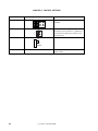
User’s Manual
IE-703107-MC-EM1
In-Circuit Emulator Option Board
Target Devices
V850E/MA1
V850E/MA2
Document No.
Date Published
©
Printed in Japan
U14481EJ3V0UM00 (3rd edition)
August 2004 NS CP(K)
[MEMO]
2
User’s Manual U14481EJ3V0UM
Windows is either a registered trademark or a trademark of Microsoft Corporation in the United States
and/or other countries.
PC/AT is a trademark of International Business Machines Corporation.
• The information in this document is current as of August, 2004. The information is subject to
change without notice. For actual design-in, refer to the latest publications of NEC Electronics data
sheets or data books, etc., for the most up-to-date specifications of NEC Electronics products. Not
all products and/or types are available in every country. Please check with an NEC Electronics sales
representative for availability and additional information.
• No part of this document may be copied or reproduced in any form or by any means without the prior
written consent of NEC Electronics. NEC Electronics assumes no responsibility for any errors that may
appear in this document.
• NEC Electronics does not assume any liability for infringement of patents, copyrights or other intellectual
property rights of third parties by or arising from the use of NEC Electronics products listed in this document
or any other liability arising from the use of such products. No license, express, implied or otherwise, is
granted under any patents, copyrights or other intellectual property rights of NEC Electronics or others.
• Descriptions of circuits, software and other related information in this document are provided for illustrative
purposes in semiconductor product operation and application examples. The incorporation of these
circuits, software and information in the design of a customer's equipment shall be done under the full
responsibility of the customer. NEC Electronics assumes no responsibility for any losses incurred by
customers or third parties arising from the use of these circuits, software and information.
• While NEC Electronics endeavors to enhance the quality, reliability and safety of NEC Electronics products,
customers agree and acknowledge that the possibility of defects thereof cannot be eliminated entirely. To
minimize risks of damage to property or injury (including death) to persons arising from defects in NEC
Electronics products, customers must incorporate sufficient safety measures in their design, such as
redundancy, fire-containment and anti-failure features.
• NEC Electronics products are classified into the following three quality grades: "Standard", "Special" and
"Specific".
The "Specific" quality grade applies only to NEC Electronics products developed based on a customerdesignated "quality assurance program" for a specific application. The recommended applications of an NEC
Electronics product depend on its quality grade, as indicated below. Customers must check the quality grade of
each NEC Electronics product before using it in a particular application.
"Standard": Computers, office equipment, communications equipment, test and measurement equipment, audio
and visual equipment, home electronic appliances, machine tools, personal electronic equipment
and industrial robots.
"Special": Transportation equipment (automobiles, trains, ships, etc.), traffic control systems, anti-disaster
systems, anti-crime systems, safety equipment and medical equipment (not specifically designed
for life support).
"Specific": Aircraft, aerospace equipment, submersible repeaters, nuclear reactor control systems, life
support systems and medical equipment for life support, etc.
The quality grade of NEC Electronics products is "Standard" unless otherwise expressly specified in NEC
Electronics data sheets or data books, etc. If customers wish to use NEC Electronics products in applications
not intended by NEC Electronics, they must contact an NEC Electronics sales representative in advance to
determine NEC Electronics' willingness to support a given application.
(Note)
(1) "NEC Electronics" as used in this statement means NEC Electronics Corporation and also includes its
majority-owned subsidiaries.
(2) "NEC Electronics products" means any product developed or manufactured by or for NEC Electronics (as
defined above).
M8E 02. 11-1
User’s Manual U14481EJ3V0UM
3
Regional Information
Some information contained in this document may vary from country to country. Before using any NEC
Electronics product in your application, pIease contact the NEC Electronics office in your country to
obtain a list of authorized representatives and distributors. They will verify:
•
Device availability
•
Ordering information
•
Product release schedule
•
Availability of related technical literature
•
Development environment specifications (for example, specifications for third-party tools and
components, host computers, power plugs, AC supply voltages, and so forth)
•
Network requirements
In addition, trademarks, registered trademarks, export restrictions, and other legal issues may also vary
from country to country.
[GLOBAL SUPPORT]
http://www.necel.com/en/support/support.html
NEC Electronics America, Inc. (U.S.)
NEC Electronics (Europe) GmbH
NEC Electronics Hong Kong Ltd.
Santa Clara, California
Tel: 408-588-6000
800-366-9782
Duesseldorf, Germany
Tel: 0211-65030
Hong Kong
Tel: 2886-9318
• Sucursal en España
Madrid, Spain
Tel: 091-504 27 87
• Succursale Française
Vélizy-Villacoublay, France
Tel: 01-30-67 58 00
• Filiale Italiana
Milano, Italy
Tel: 02-66 75 41
• Branch The Netherlands
Eindhoven, The Netherlands
Tel: 040-244 58 45
• Tyskland Filial
NEC Electronics Hong Kong Ltd.
Seoul Branch
Seoul, Korea
Tel: 02-558-3737
NEC Electronics Shanghai Ltd.
Shanghai, P.R. China
Tel: 021-5888-5400
NEC Electronics Taiwan Ltd.
Taipei, Taiwan
Tel: 02-2719-2377
NEC Electronics Singapore Pte. Ltd.
Novena Square, Singapore
Tel: 6253-8311
Taeby, Sweden
Tel: 08-63 80 820
• United Kingdom Branch
Milton Keynes, UK
Tel: 01908-691-133
J04.1
4
User’s Manual U14481EJ3V0UM
General Precautions on Handling This Product
1. Cases in which NEC Electronics warranty does not apply
• When the product is disassembled, reconstructed, or modified by the user
• When the product receives a heavy shock such as being dropped or falling down
• When the product is used with excessive voltage or is stored outside the guaranteed temperature
range or guaranteed humidity range
• When power is applied while the AC adapter, interface cable, or target system is not connected
securely
• When the AC adapter cable, PC interface cable, or extension probe is excessively twisted or
stretched
• When an AC adapter other than the one supplied with the product is used
• When water is spilled on the product
• When the product and target system are connected in a system in which the voltage potential
between the GND of the product and the target system GND differ
• When the connector or cable is connected or disconnected while the power is being applied to the
product
• When an excessive load is applied to the connector or socket
2. Cautions on safe use
• The product heats up (to approx. 50 to 60°C) when it operates for a long time. Take care not to
receive injuries such as burns from a rise in the temperature.
• Be very careful to avoid electric shocks. There is a danger of electrical shock if the product is used
as described above in 1. Cases in which NEC Electronics warranty does not apply.
User’s Manual U14481EJ3V0UM
5
INTRODUCTION
Target Readers
This manual is intended for users who design and develop application systems
using the V850E/MA1 and V850E/MA2.
Purpose
The purpose of this manual is to describe the proper operation of the IE-703107-MCEM1, and its basic specifications.
Organization
This manual is broadly divided into the following parts.
• Overview
• Names and functions of components
• Factory settings
• Cautions
• Differences between target devices and target interface circuits
How to Read This Manual
It is assumed that the reader of this manual has general knowledge of electrical
engineering, logic circuits, and microcontrollers.
The IE-703107-MC-EM1 is used connected to the IE-V850E-MC-A in-circuit
emulator. This manual explains the basic setup procedure and switch settings
of the IE-703107-MC-EM1. For the names and functions, and the connection of
parts, refer to the IE-V850E-MC, IE-V850E-MC-A User’s Manual (U14487E),
which is a separate volume.
To understand the basic specifications and operation methods broadly
→ Read this manual in the order listed in CONTENTS.
To know the operation methods and command functions of the IE-V850E-MC-A and
IE-703107-MC-EM1
→ Read the user’s manual of the debugger (separate volume) that is used.
The mark
Conventions
shows major revised points.
Note:
Footnote for item marked with Note in the text
Caution:
Information requiring particular attention
Remark:
Supplementary information
Binary … ×××× or ××××B
Numeral representations:
Decimal … ××××
Hexadecimal … ××××H
Prefixes representing the power of 2 (address space, memory capacity):
K (kilo): 210 = 1024
M (mega): 220 = 10242
6
User’s Manual U14481EJ3V0UM
Terminology
The meanings of terms used in this manual are listed below.
Target device
This is the device to be emulated.
Target system
The system (user-built system) to be debugged. This includes the target program and
hardware configured by the user.
Related Documents
When using this manual, refer to the following manuals.
The related documents indicated in this publication may include preliminary versions.
However, preliminary versions are not marked as such.
{ Documents related to development tools (user’s manuals)
Product Name
Document Number
IE-V850E-MC, IE-V850E-MC-A (In-Circuit Emulator)
U14487E
IE-703107-MC-EM1 (In-Circuit Emulator Option Board)
This manual
V850E/MA1 Hardware
U14359E
V850E/MA2 Hardware
U14980E
V850 Series Development Tools (Supporting 32-Bit OS) Windows
TM
Tutorial Guide
U16544E
Operation
U16932E
C Language
U16930E
Assembly Language
U16931E
Link Directives
U16933E
Based (Application Note)
CA850 Ver. 2.70 C Compiler Package
PM plus Ver.5.20
U16934E
ID850 (Ver.2.50 or later) (Integrated Debugger)
Operation
U16217E
SM850 (Ver.2.50 or later) (System Simulator)
Operation
U16218E
RX850 (Real-Time OS)
Basics
U13430E
Installation
U13410E
Basics
U13773E
Installation
U13774E
RX850 Pro (Real-Time OS)
RD850 (Ver. 3.01) (Task Debugger)
U13737E
RD850 Pro (Ver. 3.01) (Task Debugger)
U13916E
AZ850 (System Performance Analyzer)
U14410E
PG-FP4 (Flash Memory Programmer)
U15260E
User’s Manual U14481EJ3V0UM
7
CONTENTS
CHAPTER 1 OVERVIEW..........................................................................................................................10
1.1
1.2
1.3
1.4
1.5
1.6
Hardware Configuration .............................................................................................................11
Hardware Specifications (When Connected to IE-V850E-MC-A)............................................12
System Specifications of IE-703107-MC-EM1 (When Connected to IE-V850E-MC-A)..........13
System Configuration.................................................................................................................14
Contents in Carton......................................................................................................................17
Connection Between IE-V850E-MC-A and IE-703107-MC-EM1...............................................18
CHAPTER 2 NAMES AND FUNCTIONS OF COMPONENTS ............................................................20
2.1
2.2
2.3
2.4
Names and Functions of IE-703107-MC-EM1 Components ....................................................21
Clock Settings .............................................................................................................................23
2.2.1
Outline of clock settings .................................................................................................................23
2.2.2
Clock setting methods ....................................................................................................................24
Operation Mode Settings............................................................................................................28
Power Supply Settings ...............................................................................................................29
2.4.1
2.5
JP2 setting when emulator operates as stand-alone unit ...............................................................29
Emulation Memory ......................................................................................................................30
2.5.1
Wait setting for emulation memory .................................................................................................30
2.5.2
Cautions related to emulation memory...........................................................................................31
CHAPTER 3 FACTORY SETTINGS........................................................................................................32
CHAPTER 4 CAUTIONS ..........................................................................................................................33
4.1
4.2
Cautions on Terminating Pins ...................................................................................................33
Notes on Internal RAM................................................................................................................34
CHAPTER 5 DIFFERENCES BETWEEN TARGET DEVICES AND TARGET INTERFACE
CIRCUITS............................................................................................................................35
APPENDIX A DIMENSIONS.....................................................................................................................48
A.1
A.2
Corresponding Package Dimensions .......................................................................................48
Conditions for Connecting of In-Circuit Emulator Option Board and Conversion
Connector ....................................................................................................................................66
APPENDIX B EXAMPLE OF USE OF CONNECTOR FOR TARGET CONNECTION ....................69
APPENDIX C CONNECTORS FOR TARGET CONNECTION .............................................................70
C.1
C.2
C.3
C.4
C.5
C.6
8
Usage (LQFP Package)...............................................................................................................70
Cautions on Handling Connectors (LQFP Package) ...............................................................72
Notes on Board Design (FBGA Package) .................................................................................73
Soldering CSSOCKET (Main Enclosure Connector) to Target Board (FBGA Package)......74
Using LSPACK to Mount IC (FBGA Package) ..........................................................................76
Connecting In-Circuit Emulator (FBGA Package) ...................................................................77
User’s Manual U14481EJ3V0UM
C.7
Notes on Handling LSPACK/CSSOCKET (FBGA Package)....................................................78
APPENDIX D INSERTING PLASTIC SPACER .....................................................................................79
APPENDIX E REVISION HISTORY ........................................................................................................80
User’s Manual U14481EJ3V0UM
9
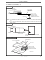
CHAPTER 1 OVERVIEW
The IE-703107-MC-EM1 is an option board for the in-circuit emulator IE-V850E-MC-A. By connecting the IE703107-MC-EM1 to IE-V850E-MC-A, hardware and software can be debugged efficiently in system development
using the V850E/MA1 and V850E/MA2.
In this manual, the basic setup sequences and switch settings of the IE-703107-MC-EM1 when connecting it to the
IE-V850E-MC-A are described.
For the names and functions of the parts of the IE-V850E-MC-A, and for the
connection of elements, refer to the IE-V850E-MC, IE-V850E-MC-A User’s Manual (U14487E) which is a separate
volume.
10
User’s Manual U14481EJ3V0UM
CHAPTER 1 OVERVIEW
1.1
Hardware Configuration
Separately-sold hardware
In-circuit emulator (IE-V850E-MC-A)
Option board
(IE-703107-MC-EM1)
IE-V850E-MC-A can be used as in-circuit emulator for
V850E/MA1 and V850E/MA2 by adding this board.
Separately-sold hardware
Extension probes
General-purpose extension probes made by TOKYO
ELETECH CORPORATION.
SC: Flexible probe
SWEX: Coaxial probe
Note 1
SC-xxxSDN
SWEX-xxxSD-1Note 1
These boards are used to connect the
IE-V850E-MC-A to a personal computer.
These boards are inserted in the expansion slot of
the personal computer.
IE-70000-PCI-IF (-A): For PCI bus
IE-70000-CD-IF-A: For PCMCIA socket
PC interface boards
IE-70000-PCI-IF (-A)
IE-70000-CD-IF-A
Power adapter
AC adapter dedicated to NEC Electronics in-circuit
emulators.
(IE-70000-MC-PS-B)
Conversion socket for V850E/MA1
(161-pin FBGA)
Socket for conversion into foot pattern of FBGA when
the 161-pin FBGA package is used.
CSSOCKET161A1413N01NNote 1
CSSOCKET161A1413N01S1Note 1
LSPACK161A1413N01Note 1
CSICE161A1413N02Note 1
YQGUIDENote 1
Conversion socket for V850E/MA2
(100-pin LQFP)
Socket for conversion into foot pattern of 100-pin
LQFP when the V850E/MA2 is used.
VP-V850E/MA1-MA2Note 2
NQPACK100SDNote 1
YQPACK100SDNote 1
HQPACK100SDNote 1
YQGUIDENote 1
Notes 1. For further information, contact Daimaru Kogyo Co., Ltd.
Tokyo Electronics Department (TEL +81-3-3820-7112)
Osaka Electronics Department (TEL +81-6-6244-6672)
2. For further information, contact Naito Densei Machida Mfg. Co., Ltd. (TEL +81-45-475-4191)
User’s Manual U14481EJ3V0UM
11
CHAPTER 1 OVERVIEW
1.2
Hardware Specifications (When Connected to IE-V850E-MC-A)
Table 1-1. Hardware Specifications
Parameter
Value
Target device
V850E/MA1
µPD703103AGJ-UEN
µPD703105AGJ-xxx-UEN
µPD703106AGJ-xxx-UEN
µPD703107AGJ-xxx-UEN
µPD70F3107AGJ-UEN
µPD703106AF1-xxx-EN4
µPD703107AF1-xxx-EN4
µPD70F3107AF1-EN4
µPD703106AGJ(A)-xxx-UEN
µPD703107AGJ(A)-xxx-UEN
µPD70F3107AGJ(A)-xxx-UEN
V850E/MA2
µPD703108GC-8EU
VDD = AVDD = CVDD = AVREF = 3.3 ±0.3 V
Target board interface voltage
VSS = AVSS = CVSS = 0 V
Maximum operation frequency
50 MHz (40 MHz when the in-circuit emulator is used for the
V850E/MA2)
External dimensions
(refer to APPENDIX A DIMENSIONS)
Height
15 mm
Length
206 mm
Width
96 mm
Power consumption
9.1 W (Max.)
Weight
190 g
Remark
“xxx” indicates ROM code suffix.
{ Extremely lightweight and compact
{ Higher equivalence with target device can be achieved by omitting buffer between signal cables.
{ External data of 8 bits can be traced by connecting an external logic probe (included).
{ The following pins can be masked.
RESET, NMI, WAIT, HLDRQ, STOP
12
User’s Manual U14481EJ3V0UM
CHAPTER 1 OVERVIEW
1.3
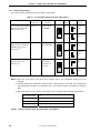
System Specifications of IE-703107-MC-EM1 (When Connected to IE-V850E-MC-A)
Table 1-2. System Specifications of IE-703107-MC-EM1 (When Connected to IE-V850E-MC-A)
Parameter
Emulation memory
capacity
Execution/pass detection
Specification
Internal ROM
1 MB (Max.)
External memory
4 MB (Max.)
Internal ROM
1 MB (Max.)
Real-time execution function
Go, execution from cursor position, automatic go, execution up
coverage
Program execution
function
to cursor position, restart, return out
Non-real-time execution function
Break function
Step-in, next over, slow-motion
Event detection break, software break, forced break, break via
come function, break on condition met during step execution,
failsafe break
Trace function
Other functions
Trace condition
All trace, section trace, qualify trace
Memory capacity
168 bits × 32 K frames
Mapping function, event function, snapshot function, stub
function, register manipulation function, memory manipulation
function, time measurement function, real-time RAM sampling
function
Caution
Some of the functions may not be supported depending on the debugger used.
User’s Manual U14481EJ3V0UM
13
CHAPTER 1 OVERVIEW
1.4
System Configuration
The system configuration when connecting the IE-703107-MC-EM1 to the IE-V850E-MC-A, which is then
connected to a personal computer (PC-9800 series, PC/ATTM or compatible) is shown below.
• V850E/MA1 (144-pin LQFP): Refer to Figure 1-1.
• V850E/MA1 (161-pin FBGA): Refer to Figure 1-2.
• V850E/MA2 (100-pin LQFP): Refer to Figure 1-3.
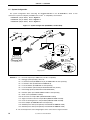
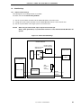
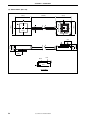
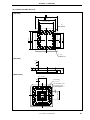
Figure 1-1. System Configuration (V850E/MA1, 144-Pin LQFP)
<14>
<5>
<15>
<6>
<7>
<13>
<4>
<9>
<8>
<10>
<9>
<3>
Target
system
<11>
<10>
<12>
<11>
V850E/MA1
(144-pin LQFP)
<1>, <2>
<12>
<11>
Target system
Remarks 1. <1> Personal computer (PC-9800 series, PC/AT or compatible)
<2> Debugger (sold separately), device file
<3> PC interface board (IE-70000-PCI-IF(-A), IE-70000-CD-IF-A: sold separately)
<4> PC interface cable (included with IE-V850E-MC-A)
<5> In-circuit emulator (IE-V850E-MC-A: sold separately)
<6> In-circuit emulator option board (IE-703107-MC-EM1: this product)
<7> External logic probe (included with IE-703107-MC-EM1)
<8> Extension probe (SC-144SDN, SWEX-144SD-1: sold separately)
<9> Guide screws (YQGUIDE: included)
<10> IE connector for 144-pin LQFP (YQPACK144SD: included)
<11> Target connection socket for 144-pin LQFP (NQPACK144SD: included)
<12> Cover for mounting device in 144-pin LQFP (HQPACK144SD: included)
<13> Power adapter (IE-70000-MC-PS-B: sold separately)
<14> AC100 V power cable (sold separately: included with IE-70000-MC-PS-B)
<15> AC220 V power cable (sold separately: included with IE-70000-MC-PS-B)
2. The encircled portions show enlarged figures of the connectors for target connection.
14
User’s Manual U14481EJ3V0UM
Target
system
CHAPTER 1 OVERVIEW
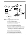
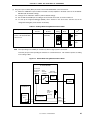
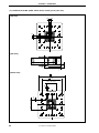
Figure 1-2. System Configuration (V850E/MA1, 161-Pin FBGA)
<19>
<5>
<20>
<6>
<7>
<18>
<4>
<14>
<15>
<8>
<9>
<10>
<3>
V850E/MA1
(161-pin FBGA)
<16>
<17>
<11>
<12>
<13>
<14><15>
<11><16><17>
Target
system
<13>
<1>, <2>
<9>
<10><11>
<13>
Target
system
Target system
Remarks 1. <1> Personal computer (PC-9800 series, PC/AT or compatible)
<2> Debugger (sold separately), device file
<3> PC interface board (IE-70000-PCI-IF(-A), IE-70000-CD-IF-A: sold separately)
<4> PC interface cable (included with IE-V850E-MC-A)
<5> In-circuit emulator (IE-V850E-MC-A: sold separately)
<6> In-circuit emulator option board (IE-703107-MC-EM1: this product)
<7> External logic probe (included with IE-703107-MC-EM1)
<8> Extension probe (SC-144SDN, SWEX-144SD-1: sold separately)
<9> Guide screws (YQGUIDE: included)
<10> IE connector for 161-pin FBGA (CSICE161A1413N02: sold separately)
<11> Pogo pin connector for 161-pin FBGA (LSPACK161A1413N01: sold separately)
<12> Stacking socket for 161-pin FBGA (option) (CSSOCKET161A1413N01S1: sold separately)
<13> Target connection socket for 161-pin FBGA (CSSOCKET161A1413N01N: sold separately)
This is a type of target connection socket without guide pins.
The type of target connection socket with guide pins is the CSSOCKET161A1413N01.
<14> Screw for mounting device (included with LSPACK161A1413N01)
<15> Cover for mounting device (included with LSAPCK161A1413N01)
<16> Spacer for mounting device (included with LSPACK161A1413N01)
<17> Guide plate for mounting device (included with LSPACK161A1413N01)
<18> Power adapter (IE-70000-MC-PS-B: sold separately)
<19> AC100 V power cable (sold separately: included with IE-70000-MC-PS-B)
<20> AC220 V power cable (sold separately: included with IE-70000-MC-PS-B)
2. The encircled portions show enlarged figures of the connectors for target connection.
User’s Manual U14481EJ3V0UM
15
CHAPTER 1 OVERVIEW
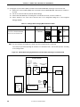
Figure 1-3. System Configuration (V850E/MA2, 100-Pin LQFP)
<15>
<5>
<16>
<6>
<7>
<14>
<8>
<4>
<11>
<9>
<3>
<12>
Target
system
<10>
<11>
V850E/MA2
(100-pin LQFP)
<1>, <2>
<12>
<13>
<13>
<12>
Target
system
Target system
Remarks 1. <1> Personal computer (PC-9800 series, PC/AT or compatible)
<2> Debugger (sold separately), device file
<3> PC interface board (IE-70000-PCI-IF(-A), IE-70000-CD-IF-A: sold separately)
<4> PC interface cable (included with IE-V850E-MC-A)
<5> In-circuit emulator (IE-V850E-MC-A: sold separately)
<6> In-circuit emulator option board (IE-703107-MC-EM1: this product)
<7> External logic probe (included with IE-703107-MC-EM1)
<8> 144-pin to 100-pin conversion adapter (VP-V850E/MA1-MA2: sold separately)
<9> Extension probe (SC-100SDN, SWEX-100SD-1: sold separately)
<10> Guide screws (YQGUIDE: included)
<11> IE connector for 100-pin LQFP (YQPACK100SD: included with VP-V850E/MA1-MA2)
<12> Target connection socket for 100-pin LQFP (NQPACK100SD: included with VP-V850E/MA1MA2)
<13> Cover for mounting device in 100-pin LQFP (HQPACK100SD: included with VP-V850E/MA1MA2)
<14> Power adapter (IE-70000-MC-PS-B: sold separately)
<15> AC100 V power cable (sold separately: included with IE-70000-MC-PS-B)
<16> AC220 V power cable (sold separately: included with IE-70000-MC-PS-B)
2. The encircled portions show enlarged figures of the connectors for target connection.
16
User’s Manual U14481EJ3V0UM
CHAPTER 1 OVERVIEW
1.5
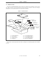
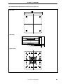
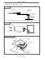
Contents in Carton
The carton of the IE-703107-MC-EM1 contains the main unit, a guarantee card, a packing list, and an accessory
bag. Make sure that the accessory bag contains this manual and connector accessories. In the case of missing or
damaged items, contact an NEC Electronics sales representative or distributor.
Figure 1-4. Contents in Carton
<2> Accessory bag
<1> IE-703107-MC-EM1
<5> IC socket
NQPACK144SD
<4> Packing list
<6> IC socket
YQPACK144SD
<3> Guarantee card
<7> IC socket
HQPACK144SD
<8> Guide screws
YQGUIDE
<1> IE-703107-MC-EM1 × 1
<5> IC socket NQPACK144SD × 1
<2> Accessory bag × 1
<6> IC socket YQPACK144SD × 1
<3> Guarantee card × 1
<7> IC socket HQPACK144SD × 1
<4> Packing list × 1
<8> Guide screws YQGUIDE × 4
Check that the accessory bag contains this manual, a packing list, an external logic probe, and a restriction
document.
User’s Manual U14481EJ3V0UM
17
CHAPTER 1 OVERVIEW
1.6
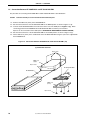
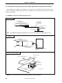
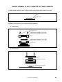
Connection Between IE-V850E-MC-A and IE-703107-MC-EM1
The procedure for connecting the IE-V850E-MC-A and IE-703107-MC-EM1 is described below.
Caution
Connect carefully so as not to break or bend connector pins.
<1> Remove the POD cover (lower) of the IE-V850E-MC-A.
<2> Set the PGA socket lever of the IE-703107-MC-EM1 to the OPEN position as shown in Figure 1-5 (b).
<3> Connect the IE-703107-MC-EM1 to the PGA socket at the rear of the POD (refer to Figure 1-5 (c)). When
connecting, position the IE-V850E-MC-A and IE-703107-MC-EM1 so that they are horizontal.
Spacers can be connected to fix the POD (refer to APPENDIX D MOUNTING OF PLASTIC SPACER).
<4> Set the PGA socket lever of the IE-703107-MC-EM1 to the CLOSE position as shown in Figure 1-5 (b).
<5> Fix the POD cover (lower) to the soldered side of the IE-703107-MC-EM1 using the nylon rivets supplied with
the IE-V850E-MC-A.
Figure 1-5. Connection Between IE-V850E-MC-A and IE-703107-MC-EM1 (1/2)
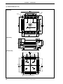
(a) Connection overview
Nylon rivets
POD cover
(upper)
Nylon rivets
IE-703107-MC-EM1
IE-V850E-MC-A
POD cover
(lower)
Nylon rivets
18
User’s Manual U14481EJ3V0UM
CHAPTER 1 OVERVIEW
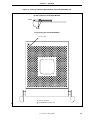
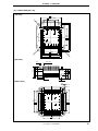
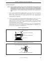
Figure 1-5. Connection Between IE-V850E-MC-A and IE-703107-MC-EM1 (2/2)
(b) PGA socket lever of IE-703107-MC-EM1
CLOSE
OPEN
(c) Connecting part (IE-703107-MC-EM1)
Pin A1 location
: Insertion guide pin
: IE-V850E-MC-A insertion area
User’s Manual U14481EJ3V0UM
19
CHAPTER 2 NAMES AND FUNCTIONS OF COMPONENTS
This chapter describes the names, functions, and switch settings of components comprising the IE-703107-MCEM1. For the details of the pod, jumper, and switch positions, etc., refer to the IE-V850E-MC, IE-V850E-MC-A User’s
Manual (U14487E).
20
User’s Manual U14481EJ3V0UM
CHAPTER 2 NAMES AND FUNCTIONS OF COMPONENTS
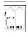
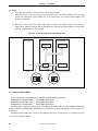
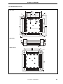
2.1
Names and Functions of IE-703107-MC-EM1 Components
Figure 2-1. IE-703107-MC-EM1
Direction of pin 1 of
the connector for
target connection
Connector for
target connection
Connector for
target connection
LD2
LD1
DIRECT
SW1
D70F3107
TP1
TP2
TP3
TP4
TP5
TP6
TP7
PLL
JP1
JP2
OSC
1
2 1
3
7
8
2
4
CN1
Connector for connecting
IE-V850E-MC-A
Emulation memory
User’s Manual U14481EJ3V0UM
21
CHAPTER 2 NAMES AND FUNCTIONS OF COMPONENTS
(1) Test pins (TP1 to TP7)
To leave the DMA cycle or refresh cycle in the tracer, or cause a break, connect these pins to the external logic
probe.
• TP1:
• TP2:
• TP3:
• TP4:
• TP5:
• TP6:
• TP7:
GND
REFRQ
DMAAK0
DMAAK1
DMAAK2
DMAAK3
Test pin for product shipment inspection
(2) SW1
This is a switch for clock mode switching (for details, refer to 2.2 Clock Settings).
(3) JP1
This is a jumper for switching the clock supply source (for details, refer to 2.2 Clock Settings).
(4) JP2
This is a jumper for switching the power supply (for details, refer to 2.4 Power Supply Settings).
(5) CN1
Connects the external logic probe (included).
(6) LD1 (CKSEL: Green)
This LED indicates the level input to the CKSEL pin. If the target system is not connected, whether this LED lights
or not is determined by the setting of SW1.
LED Status
When Used as Stand-Alone Unit
When Used Connected to Target System
Lit
SW1 = DIRECT
The CKSEL signal from the target system is high
Extinguished
SW1 = PLL
The CKSEL signal from the target system is low
(7) LD2 (RUN: Yellow)
This LED indicates whether the program is under execution.
LED Status
Meaning
Lit
User program is being executed.
Extinguished
User program is halted.
(8) Connector for IE-V850E-MC-A connection
This is a connector for connecting the IE-V850E-MC-A.
(9) Connector for target connection
This is a connector for connecting the target system or the extension probe.
(10) Emulation memory
This is a memory that replaces the memory/memory mapped I/O on the target system (for details, refer to 2.5
Emulation Memory).
22
User’s Manual U14481EJ3V0UM
CHAPTER 2 NAMES AND FUNCTIONS OF COMPONENTS
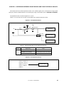
2.2
Clock Settings
2.2.1 Outline of clock settings
The following three clock setting methods are available.
For details, refer to 2.2.2 Clock setting methods.
(1) Use the crystal oscillator mounted on the IE-703107-MC-EM1 as the internal clock.
(2) Change the crystal oscillator mounted on the IE-703107-MC-EM1 and use it as the internal clock.
(3) Use the crystal oscillator on the target system as an external clock.
Caution
When using an external clock, input a square wave to the X1 pin.
When a clock generated by a crystal/ceramic resonator is used, the IE-703107-MC-EM1 does not
operate.
Figure 2-2. Outline of Clock Settings
IE-703107-MC-EM1
Switching internal/
external clock
Crystal oscillator
(can be changed)
Target system
OSC
JP1
X1
Crystal
oscillator
IE-V850E-MC-A
Emulation CPU
SW1
PLL/direct
mode
switching
µPD70F3107
CKSEL
CLKOUT
User’s Manual U14481EJ3V0UM
23
CHAPTER 2 NAMES AND FUNCTIONS OF COMPONENTS
2.2.2 Clock setting methods
A list of the hardware settings for each clock setting is shown below.
Table 2-1. List of Hardware Settings for Each Clock Setting
Type of Clock Used
Selection
(1) Use crystal oscillator (OSC)
OSC Crystal
Clock Source
Note 1
Internal
JP1 Setting
Oscillator
Factory setting
mounted on IE-703107-MC-
(5.000 MHz)
Clock
SW1
Mode
1
2
PLL
CKSEL
Pin
PLL
Note 2
Low-level
input
EM1 as internal clock.
Direct
Direct
PLL
High-level
input
(2) Change crystal oscillator
Internal
Change (to other
than 5.000 MHz)
(OSC) mounted on IE-703107-
7
8
1
2
Direct
PLL
PLL
Low-level
input
MC-EM1 and use it as the
Direct
Note 3
internal clock
.
Direct
PLL
High-level
input
(3) Use the crystal oscillator on
External
Crystal oscillator
the target system as an
can be either
external clock.
mounted or not
7
8
1
2
Direct
PLL
PLL
Low-level
input
Direct
mounted
Direct
PLL
High-level
input
7
8
Direct
Notes 1. Select the clock source in the clock source selection area in the configuration dialog box on the
debugger.
2. The input setting to the CKSEL pin is made only when a target system is connected. Leave this pin open
when operating the emulator on a stand-alone basis. The emulator operates according to the setting of
SW1.
3. When replacing the crystal oscillator on the emulator, use an oscillator with the following specifications.
Caution
24
Power supply voltage
5V
Output level
CMOS
Shape
8-pin type
Pin layout
Pin 1: NC Pin 4: GND Pin 5: OUT Pin 8: VDD
Settings other than those described above are prohibited.
User’s Manual U14481EJ3V0UM
CHAPTER 2 NAMES AND FUNCTIONS OF COMPONENTS
(1) Using the crystal oscillator (OSC) mounted on the IE-703107-MC-EM1 as the internal clock
<1> Mount the 5.000 MHz crystal oscillator mounted at factory shipment in the OSC socket of the IE-703107MC-EM1 (with the default settings).
<2> Change JP1 as indicated in Table 2-2 (with the default settings).
<3> Set the SW1 and CKSEL pins according to the clock mode to be used, as shown in Table 2-2.
<4> To start up the integrated debugger (ID850), select “Internal” in the clock source selection area in the
configuration dialog box (clock selection in emulator).
Table 2-2. Settings When Using Mounted Internal Clock
Type of Clock Used
Use crystal oscillator (OSC)
Clock Source
OSC Crystal
JP1
Clock
Selection
Oscillator
Setting
Mode
Internal
1
Factory setting
mounted on IE-703107-MC-EM1
2
SW1
CKSEL
Pin
PLL
PLL
Note
Low-level
input
(5.000 MHz)
as internal clock.
Direct
Direct
PLL
High-level
input
7
8
Direct
Note The input setting to the CKSEL pin is made only when a target system is connected.
Leave this pin open when operating the emulator on a stand-alone basis. The emulator operates according
to the setting of SW1.
Figure 2-3. Outline When Using Mounted Internal Clock
IE-703107-MC-EM1
1-2 shorted
3-4 shorted
5-6 open
7-8 open
Select
“Internal”
on ID850
Mounted
crystal oscillator
Target system
OSC
5 MHz
JP1
X1
Crystal
oscillator
IE-V850E-MC-A
SW1
PLL/direct
mode
switching
Emulation
CPU
µPD70F3107
CKSEL
CLKOUT
User’s Manual U14481EJ3V0UM
25
CHAPTER 2 NAMES AND FUNCTIONS OF COMPONENTS
(2) Changing the crystal oscillator (OSC) mounted on the IE-703107-MC-EM1 and using it as the internal clock
<1> Remove the crystal oscillator (OSC) that is mounted on the IE-703107-MC-EM1 and mount the oscillator to
be used.
<2> Set JP1 as shown in Table 2-3 (with the default settings).
<3> Set the SW1 and CKSEL pins according to the clock mode to be used, as shown in Table 2-3.
<4> Select “Internal” in the clock source selection area in the configuration dialog box on the integrated
debugger (ID850).
Table 2-3. Settings When Changing Mounted Internal Clock
Type of Clock Used
Change the crystal oscillator
Clock Source
OSC Crystal
JP1
Clock
Selection
Oscillator
Setting
Mode
Internal
Change (to other
mounted on IE-703107-MC-EM1
1
2
SW1
CKSEL
Pin
PLL
PLL
Note
Low-level
input
than 5.000 MHz)
and use it as the internal clock.
Direct
Direct
PLL
High-level
input
7
8
Direct
Note The input setting to the CKSEL pin is made only when a target system is connected.
Leave this pin open when operating the emulator on a stand-alone basis. The emulator operates according
to the setting of SW1.
Figure 2-4. Outline When Changing Mounted Crystal Oscillator and Using It as Internal Clock
IE-703107-MC-EM1
1-2 shorted
3-4 shorted
5-6 open
7-8 open
Select
“Internal”
on ID850
Change crystal
oscillator
OSC
other than
5 MHz
JP1
Target system
X1
IE-V850E-MC-A
SW1
PLL/direct
mode
switching
Emulation
CPU
µPD70F3107
CKSEL
CLKOUT
26
User’s Manual U14481EJ3V0UM
Crystal
oscillator
CHAPTER 2 NAMES AND FUNCTIONS OF COMPONENTS
(3) Using the target system crystal oscillator as an external clock
<1> Set JP1 as shown in Table 2-5 (with the default setting).
<2> Set the SW1 and CKSEL pins according to the clock mode to be used, as shown in Table 2-5.
<3> Select “External” in the clock source selection area in the configuration dialog box on the integrated
debugger (ID850).
Table 2-4. Settings When Using External Clock
Type of Clock Used
Use crystal oscillator on target
Clock Source
OSC Crystal
JP1
Clock
Selection
Oscillator
Setting
Mode
External
Crystal oscillator
system as external clock.
1
2
SW1
CKSEL
Pin
PLL
PLL
can be either
Note
Low-level
input
mounted or not
Direct
mounted
Direct
PLL
High-level
input
7
8
Direct
Note The input setting to the CKSEL pin is made only when a target system is connected.
Leave this pin open when operating the emulator on a stand-alone basis. The emulator operates according
to the setting of SW1.
Caution
Be sure to input a square wave to the X1 pin.
When a clock generated by a crystal/ceramic resonator is used, the IE-703107-MC-EM1 does not
operate.
Figure 2-5. Outline When Using Crystal Oscillator on Target System as External Clock
IE-703107-MC-EM1
1-2 shorted
3-4 shorted
5-6 open
7-8 open
Select
“External”
on ID850
JP1
Target system
OSC
X1
Crystal
oscillator
IE-V850E-MC-A
SW1
PLL/direct
mode
switching
Emulation
CPU
µ PD70F3107
CKSEL
CLKOUT
User’s Manual U14481EJ3V0UM
27
CHAPTER 2 NAMES AND FUNCTIONS OF COMPONENTS
2.3
Operation Mode Settings
The IE-703107-MC-EM1 supports the following operation modes equivalent to those of the actual device. These
operation modes are selected on the debugger.
Target Device
V850E/MA1
V850E/MA2
Operation Mode
Selection in ID850
Single-chip mode 0
MODE02
Single-chip mode 1
MODE03
ROMless mode 0
MODE00
ROMless mode 1
MODE01
ROMless mode 0
MODE00
ROMless mode 1
MODE01
Note
Note Make settings in accordance with the operation mode to be used in the mask setting area of the
configuration dialog box that opens when the debugger (ID850) is started.
Caution
To operate the emulator in the ROMless mode, be sure to map the emulation memory or the
memory on the target system from address 0H.
Note that the IE-703107-MC-EM1 cannot emulate the MODE pin because the level input to the MODE pin is
realized by the pin mask function of the debugger.
For how to set the pins on the target system, refer to the V850E/MA1 Hardware User’s Manual (U14359E) or
V850E/MA2 Hardware User’s Manual (U14980E).
28
User’s Manual U14481EJ3V0UM
CHAPTER 2 NAMES AND FUNCTIONS OF COMPONENTS
2.4
Power Supply Settings
The power supply (VDD) is set by using JP2.
2.4.1 JP2 setting when emulator operates as stand-alone unit
When JP2 is set as shown in Figure 2-6, the IE-703107-MC-EM1 detects the power on the target system side and
automatically selects whether VDD is supplied from the internal power supply of the emulator or from the target system
(with the default settings).
Caution
If the JP2 setting is incorrect, the emulator may be damaged.
Figure 2-6. Setting of JP2 (for Automatic Selection of Power)
JP2Note
2 4
1 3
4
3
Set to 1-2 shorted, 3-4 open
Note A relay is used for power selection.
Depending on the combination with the target system, the relay
repeatedly turns ON/OFF when the power to the target system is turned OFF, issuing a sound continuously.
In this case, make the setting shown in Figure 2-7.
Caution
If the JP2 setting is incorrect, the emulator may be damaged.
Figure 2-7. Setting of JP2 (to Use Power from Target System)
JP2
2
4
1
3
Set to 1-2 open, 3-4 shorted
Figure 2-7 shows the setting of JP2 to supply power from the target system to VDD.
With this setting, however, note that the emulator does not operate when the target system is not connected.
User’s Manual U14481EJ3V0UM
29
CHAPTER 2 NAMES AND FUNCTIONS OF COMPONENTS
2.5
Emulation Memory
This is a substitute memory used to emulate the memory or memory mapped I/O on the target system (capacity: 4
MB).
The emulation memory is mounted on the IE-703107-MC-EM1.
2.5.1 Wait setting for emulation memory
The data wait, address wait, and idle state for the emulation memory are set as follows.
(1) ID850
Select from the following three types on the configuration screen.
Selection
WAIT MASK
Wait Type
Data wait
Emulation Memory Access
Fixed to 0 waits
External Memory Access
Depends on DWC0/1 register setting
WAIT signal masked
1 WAIT ACCESS
Address wait
Fixed to 0 waits
Depends on ASC register setting
Idle state
Fixed to 0 cycles
Depends on BCC register setting
Data wait
Fixed to 1 wait
Depends on DWC0/1 register setting
and WAIT signal status
TARGET WAIT
Address wait
Fixed to 0 waits
Depends on ASC register setting
Idle state
Fixed to 0 cycles
Depends on BCC register setting
Data wait
Depends on DWC0/1 register setting
Depends on DWC0/1 register setting
However, 1 wait when set to 0 waits
and WAIT signal status
Address wait
Fixed to 0 waits
Depends on ASC register setting
Idle state
Depends on BCC register setting
Depends on BCC register setting
(2) MULTI
Select mask or unmask for WAIT and EMWAIT using the “Pinmask” command.
Selection
WAIT: Mask
Wait Type
Data wait
Emulation Memory Access
Fixed to 0 waits
EMWAIT: Mask
WAIT: Unmask
Address wait
Fixed to 0 waits
Depends on ASC register setting
Idle state
Fixed to 0 cycles
Depends on BCC register setting
Data wait
Fixed to 1 wait
Depends on DWC0/1 register setting
and WAIT signal status
Address wait
Fixed to 0 waits
Depends on ASC register setting
Idle state
Fixed to 0 cycles
Depends on BCC register setting
Data wait
Depends on DWC0/1 register setting
Depends on DWC0/1 register setting
However, 1 wait when set to 0 waits
and WAIT signal status
Address wait
Fixed to 0 waits
Depends on ASC register setting
Idle state
Depends on BCC register setting
Depends on BCC register setting
EMWAIT: Unmask
30
Depends on DWC0/1 register setting
WAIT signal masked
EMWAIT: Mask
WAIT: Unmask
External Memory Access
User’s Manual U14481EJ3V0UM
CHAPTER 2 NAMES AND FUNCTIONS OF COMPONENTS
2.5.2 Cautions related to emulation memory
(1) Number of data waits required for emulation memory access
The number of data waits required to be inserted for emulation memory access varies depending on the operating
frequency of the emulator.
4 MHz ≤ Operating frequency < 25 MHz
0 waits
25 MHz ≤ Operating frequency ≤ 40 MHz
1 wait
40 MHz < Operating frequency
2 waits
(2) Bus sizing
Make the bus sizing 16 bits (set BSn0 of BSC register to 1).
An 8-bit bus cannot be used.
(3) WAIT pin
The number of data waits for the emulation memory is not affected by the WAIT pin.
(4) Address wait
Address waits cannot be inserted in the emulation memory.
When address waits need to be inserted, set as follows.
Number of data waits for CS
space of emulation memory
Number of address waits
=
for external memory or
external I/O
Number of data waits
+
for external memory or
external I/O
This setting is effective to make the access speed to the emulation memory equal to that of the external memory
or external I/O to measure the performance, etc.
For how to insert waits in the emulation memory, refer to 2.5.1 Wait setting for emulation memory.
User’s Manual U14481EJ3V0UM
31
CHAPTER 3 FACTORY SETTINGS
Item
Setting
Remark
JP1
All settings other than those set in the factory are
2
8
1
7
JP2
Detects the power of the target system and
JP2
2 4
1 3
prohibited.
4
3
SW1
automatically selects whether VDD is supplied from
the internal power supply of the emulator or from
the target system.
Set to PLL mode.
PLL
DIRECT
OSC
5.000 MHz crystal oscillator is mounted.
The frequency can be varied by replacing the
crystal oscillator.
32
User’s Manual U14481EJ3V0UM00
CHAPTER 4 CAUTIONS
4.1
Cautions on Terminating Pins
The pins that perform special processing in the emulator are explained below.
For detailed circuit configuration, refer to CHAPTER 5 DIFFERENCES BETWEEN TARGET DEVICES AND
TARGET INTERFACE CIRCUITS.
(1) Pins that cannot be emulated
The following pins cannot be emulated because they are left open inside the emulator or connected to 3.3 V or
GND via resistor. Evaluate these pins by using the target device.
Table 4-1. Pins That Cannot Be Emulated
Pin Name 1
MODE0
MODE1
MODE2
X2
CVDD
Target Device
Pin No.
V850E/MA1 (144-pin LQFP)
58
V850E/MA1 (161-pin FBGA)
M8
V850E/MA2 (100-pin LQFP)
36
V850E/MA1 (144-pin LQFP)
57
V850E/MA1 (161-pin FBGA)
P8
V850E/MA2 (100-pin LQFP)
35
V850E/MA1 (144-pin LQFP)
18
V850E/MA1 (161-pin FBGA)
G1
V850E/MA2 (100-pin LQFP)
21
V850E/MA1 (144-pin LQFP)
62
V850E/MA1 (161-pin FBGA)
N9
V850E/MA2 (100-pin LQFP)
40
V850E/MA1 (144-pin LQFP)
61
V850E/MA1 (161-pin FBGA)
P9
V850E/MA2 (100-pin LQFP)
39
(2) X1 pin
The X1 pin is pulled down using 33 kΩ when an external clock is selected.
Because the external clock is input to the clock generator via 74HC157, a delay time of up to 13.2 ns is
generated.
This pin is pulled down using 33 kΩ and is left open when the internal clock is selected.
(3) CKSEL pin
The CKSEL pin can be pulled up or down, depending on the setting of SW1.
It is pulled down using 33 kΩ when “PLL” is selected by SW1. This pin is pulled up using 33 kΩ when “DIRECT”
is selected.
User’s Manual U14481EJ3V0UM
33
CHAPTER 4 CAUTIONS
(4) VDD pin
<1> VDD in the target system is used to operate the circuits in the emulator.
When pins 1 and 2 of JP2 are shorted, and 3 and 4 are left open, the emulator detects VDD of the target
system and automatically selects whether VDD of the target system or the internal power supply of the
emulator is to be used.
<2> When pins 1 and 2 of JP2 are left open, and 3 and 4 are shorted, the emulator always uses VDD from the
target system. With this setting of JP2, the emulator does not operate if the target system is not connected.
However, sneaking of power can be avoided.
Figure 4-1. Schematic Diagram of Power Supply Flow
Target system
IE-703107-MC-EM1
IE-V850E-MC
µ PD70F3107
Emulation CPU
Relay
Power supply
circuit
VDD
Fixed
Automatically selected
JP2
4.2
JP2
2
4
1
3
2 4
1 3
4
3
Notes on Internal RAM
The emulator maps the internal RAM to a 12 KB space of 0xFFFC000 to 0xFFFEFFF.
V850E/MA1 (internal RAM: 4 KB):
0xFFFC000 to 0xFFFCFFF
V850E/MA1 (internal RAM: 10 KB):
0xFFFC000 to 0xFFFE7FF
V850E/MA2 (internal RAM: 4 KB):
0xFFFC000 to 0xFFFCFFF
The target device is mapped as shown above. Consequently, the higher 8 KB space (0xFFFD000 to 0xFFFEFFF)
or higher 2 KB space (0xFFFE800 to 0xFFFEFFF) of the emulator’s 12 KB internal RAM area does not exist in the
target device.
If the higher 8 KB or 2 KB space is accessed, the emulator cannot issue a fail-safe break. It is therefore necessary
to set an access break in advance.
34
User’s Manual U14481EJ3V0UM
CHAPTER 5 DIFFERENCES BETWEEN TARGET DEVICES AND TARGET INTERFACE CIRCUITS
This chapter shows the internal equivalent circuits of the emulator signals to be connected to the target system.
Some pins cannot be emulated because of the internal processing of the emulator (refer to CHAPTER 4 CAUTIONS).
The equivalent circuits are shown in Figures 5-1 to 5-10.
Tables 5-1 to 5-10 show lists of the pins corresponding to the respective equivalent circuits.
Figure 5-1. Pin Equivalent Circuit 1
5V
5V
2.5 V
µ PC358
22 Ω
74VHCT541
IE-V850E-MC-A
LED (Target)
VDD
1 kΩ
3.3 V
MA1_VDD5
Emulation CPU
Relay
µ PD70F3107
Table 5-1. Corresponding Pin List (Pin Equivalent Circuit 1)
Pin Name 1
VDD
Target Device
Pin No.
V850E/MA1 (144-pin LQFP)
8, 27, 37, 47, 81, 98, 112, 124, 134
V850E/MA1 (161-pin FBGA)
A12, C6, C8, F4, L6, F12, J3, K14, P1
V850E/MA2 (100-pin LQFP)
11, 33, 55, 83, 93
Figure 5-2. Pin Equivalent Circuit 2
PDL0 to 15, PAH0 to 9,
PCT0 and 1, PCT4 to 7,
PCD0 to 3, PAL0 to 15,
Emulation CPU
PCS0 to 7, PBD0 to 3,
PCM0 to 5
User’s Manual U14481EJ3V0UM
35
CHAPTER 5 DIFFERENCES BETWEEN TARGET DEVICES AND TARGET INTERFACE CIRCUITS
Table 5-2. Corresponding Pin List (Pin Equivalent Circuit 2) (1/5)
Pin Name 1 Pin Name 2 Pin Name 3 Pin Name 4
PDL0
PDL1
PDL2
PDL3
PDL4
PDL5
PDL6
PDL7
PDL8
PDL9
PDL10
PDL11
PDL12
PDL13
36
D0
D1
D2
D3
D4
D5
D6
D7
D8
D9
D10
D11
D12
D13
−
−
−
−
−
−
−
−
−
−
−
−
−
−
−
−
−
−
−
−
−
−
−
−
−
−
−
−
Target Device
Pin No.
V850E/MA1 (144-pin LQFP)
17
V850E/MA1 (161-pin FBGA)
G3
V850E/MA2 (100-pin LQFP)
20
V850E/MA1 (144-pin LQFP)
16
V850E/MA1 (161-pin FBGA)
H4
V850E/MA2 (100-pin LQFP)
19
V850E/MA1 (144-pin LQFP)
15
V850E/MA1 (161-pin FBGA)
F1
V850E/MA2 (100-pin LQFP)
18
V850E/MA1 (144-pin LQFP)
14
V850E/MA1 (161-pin FBGA)
F2
V850E/MA2 (100-pin LQFP)
17
V850E/MA1 (144-pin LQFP)
13
V850E/MA1 (161-pin FBGA)
F3
V850E/MA2 (100-pin LQFP)
16
V850E/MA1 (144-pin LQFP)
12
V850E/MA1 (161-pin FBGA)
E1
V850E/MA2 (100-pin LQFP)
15
V850E/MA1 (144-pin LQFP)
11
V850E/MA1 (161-pin FBGA)
G4
V850E/MA2 (100-pin LQFP)
14
V850E/MA1 (144-pin LQFP)
10
V850E/MA1 (161-pin FBGA)
E2
V850E/MA2 (100-pin LQFP)
13
V850E/MA1 (144-pin LQFP)
7
V850E/MA1 (161-pin FBGA)
E3
V850E/MA2 (100-pin LQFP)
10
V850E/MA1 (144-pin LQFP)
6
V850E/MA1 (161-pin FBGA)
C2
V850E/MA2 (100-pin LQFP)
9
V850E/MA1 (144-pin LQFP)
5
V850E/MA1 (161-pin FBGA)
D2
V850E/MA2 (100-pin LQFP)
8
V850E/MA1 (144-pin LQFP)
4
V850E/MA1 (161-pin FBGA)
E4
V850E/MA2 (100-pin LQFP)
7
V850E/MA1 (144-pin LQFP)
3
V850E/MA1 (161-pin FBGA)
B2
V850E/MA2 (100-pin LQFP)
6
V850E/MA1 (144-pin LQFP)
2
V850E/MA1 (161-pin FBGA)
C3
V850E/MA2 (100-pin LQFP)
5
User’s Manual U14481EJ3V0UM
CHAPTER 5 DIFFERENCES BETWEEN TARGET DEVICES AND TARGET INTERFACE CIRCUITS
Table 5-2. Corresponding Pin List (Pin Equivalent Circuit 2) (2/5)
Pin Name 1 Pin Name 2 Pin Name 3 Pin Name 4
PDL14
PDL15
PAH0
PAH1
PAH2
PAH3
PAH4
PAH5
PAH6
PAH7
PAH8
PAH9
PCT0
PCT1
D14
D15
A16
A17
A18
A19
A20
A21
A22
A23
A24
A25
LCAS
UCAS
−
−
−
−
−
−
−
−
−
−
−
−
LWR
UWR
−
−
−
−
−
−
−
−
−
−
−
−
LDQM
UDQM
Target Device
Pin No.
V850E/MA1 (144-pin LQFP)
1
V850E/MA1 (161-pin FBGA)
D3
V850E/MA2 (100-pin LQFP)
4
V850E/MA1 (144-pin LQFP)
144
V850E/MA1 (161-pin FBGA)
A2
V850E/MA2 (100-pin LQFP)
3
V850E/MA1 (144-pin LQFP)
123
V850E/MA1 (161-pin FBGA)
D8
V850E/MA2 (100-pin LQFP)
82
V850E/MA1 (144-pin LQFP)
122
V850E/MA1 (161-pin FBGA)
A9
V850E/MA2 (100-pin LQFP)
81
V850E/MA1 (144-pin LQFP)
121
V850E/MA1 (161-pin FBGA)
B9
V850E/MA2 (100-pin LQFP)
80
V850E/MA1 (144-pin LQFP)
120
V850E/MA1 (161-pin FBGA)
C9
V850E/MA2 (100-pin LQFP)
79
V850E/MA1 (144-pin LQFP)
119
V850E/MA1 (161-pin FBGA)
D9
V850E/MA2 (100-pin LQFP)
78
V850E/MA1 (144-pin LQFP)
118
V850E/MA1 (161-pin FBGA)
B10
V850E/MA2 (100-pin LQFP)
77
V850E/MA1 (144-pin LQFP)
117
V850E/MA1 (161-pin FBGA)
C10
V850E/MA2 (100-pin LQFP)
76
V850E/MA1 (144-pin LQFP)
116
V850E/MA1 (161-pin FBGA)
D10
V850E/MA2 (100-pin LQFP)
75
V850E/MA1 (144-pin LQFP)
115
V850E/MA1 (161-pin FBGA)
A11
V850E/MA2 (100-pin LQFP)
74
V850E/MA1 (144-pin LQFP)
114
V850E/MA1 (161-pin FBGA)
B11
V850E/MA2 (100-pin LQFP)
−
V850E/MA1 (144-pin LQFP)
97
V850E/MA1 (161-pin FBGA)
F13
V850E/MA2 (100-pin LQFP)
65
V850E/MA1 (144-pin LQFP)
96
V850E/MA1 (161-pin FBGA)
F14
V850E/MA2 (100-pin LQFP)
64
User’s Manual U14481EJ3V0UM
37
CHAPTER 5 DIFFERENCES BETWEEN TARGET DEVICES AND TARGET INTERFACE CIRCUITS
Table 5-2. Corresponding Pin List (Pin Equivalent Circuit 2) (3/5)
Pin Name 1 Pin Name 2 Pin Name 3 Pin Name 4
PCT4
PCT5
PCT6
PCT7
PCD0
PCD1
PCD2
PCD3
PAL0
PAL1
PAL2
PAL3
PAL4
PAL5
38
RD
WE
OE
BCYST
SDCKE
SDCLK
LBE
UBE
A0
A1
A2
A3
A4
A5
−
−
−
−
−
−
−
−
−
−
−
−
SDCAS
SDRAS
−
−
−
−
−
−
−
−
−
−
−
−
−
−
Target Device
Pin No.
V850E/MA1 (144-pin LQFP)
95
V850E/MA1 (161-pin FBGA)
F11
V850E/MA2 (100-pin LQFP)
63
V850E/MA1 (144-pin LQFP)
94
V850E/MA1 (161-pin FBGA)
G12
V850E/MA2 (100-pin LQFP)
62
V850E/MA1 (144-pin LQFP)
93
V850E/MA1 (161-pin FBGA)
G14
V850E/MA2 (100-pin LQFP)
−
V850E/MA1 (144-pin LQFP)
92
V850E/MA1 (161-pin FBGA)
G13
V850E/MA2 (100-pin LQFP)
−
V850E/MA1 (144-pin LQFP)
111
V850E/MA1 (161-pin FBGA)
D11
V850E/MA2 (100-pin LQFP)
73
V850E/MA1 (144-pin LQFP)
110
V850E/MA1 (161-pin FBGA)
B12
V850E/MA2 (100-pin LQFP)
72
V850E/MA1 (144-pin LQFP)
109
V850E/MA1 (161-pin FBGA)
A13
V850E/MA2 (100-pin LQFP)
71
V850E/MA1 (144-pin LQFP)
108
V850E/MA1 (161-pin FBGA)
A14
V850E/MA2 (100-pin LQFP)
70
V850E/MA1 (144-pin LQFP)
143
V850E/MA1 (161-pin FBGA)
B3
V850E/MA2 (100-pin LQFP)
2
V850E/MA1 (144-pin LQFP)
142
V850E/MA1 (161-pin FBGA)
C4
V850E/MA2 (100-pin LQFP)
1
V850E/MA1 (144-pin LQFP)
141
V850E/MA1 (161-pin FBGA)
A3
V850E/MA2 (100-pin LQFP)
100
V850E/MA1 (144-pin LQFP)
140
V850E/MA1 (161-pin FBGA)
D4
V850E/MA2 (100-pin LQFP)
99
V850E/MA1 (144-pin LQFP)
139
V850E/MA1 (161-pin FBGA)
B4
V850E/MA2 (100-pin LQFP)
98
V850E/MA1 (144-pin LQFP)
138
V850E/MA1 (161-pin FBGA)
A4
V850E/MA2 (100-pin LQFP)
97
User’s Manual U14481EJ3V0UM
CHAPTER 5 DIFFERENCES BETWEEN TARGET DEVICES AND TARGET INTERFACE CIRCUITS
Table 5-2. Corresponding Pin List (Pin Equivalent Circuit 2) (4/5)
Pin Name 1 Pin Name 2 Pin Name 3 Pin Name 4
PAL6
PAL7
PAL8
PAL9
PAL10
PAL11
PAL12
PAL13
PAL14
PAL15
PCS0
PCS1
PCS2
PCS3
A6
A7
A8
A9
A10
A11
A12
A13
A14
A15
−
−
−
−
−
−
−
−
−
−
−
−
−
−
−
−
−
−
−
−
−
−
−
−
−
−
−
−
−
−
−
−
Target Device
Pin No.
V850E/MA1 (144-pin LQFP)
137
V850E/MA1 (161-pin FBGA)
D5
V850E/MA2 (100-pin LQFP)
96
V850E/MA1 (144-pin LQFP)
136
V850E/MA1 (161-pin FBGA)
C5
V850E/MA2 (100-pin LQFP)
95
V850E/MA1 (144-pin LQFP)
133
V850E/MA1 (161-pin FBGA)
B6
V850E/MA2 (100-pin LQFP)
92
V850E/MA1 (144-pin LQFP)
132
V850E/MA1 (161-pin FBGA)
A6
V850E/MA2 (100-pin LQFP)
91
V850E/MA1 (144-pin LQFP)
131
V850E/MA1 (161-pin FBGA)
D6
V850E/MA2 (100-pin LQFP)
90
V850E/MA1 (144-pin LQFP)
130
V850E/MA1 (161-pin FBGA)
C7
V850E/MA2 (100-pin LQFP)
89
V850E/MA1 (144-pin LQFP)
129
V850E/MA1 (161-pin FBGA)
A7
V850E/MA2 (100-pin LQFP)
88
V850E/MA1 (144-pin LQFP)
128
V850E/MA1 (161-pin FBGA)
B7
V850E/MA2 (100-pin LQFP)
87
V850E/MA1 (144-pin LQFP)
127
V850E/MA1 (161-pin FBGA)
D7
V850E/MA2 (100-pin LQFP)
86
V850E/MA1 (144-pin LQFP)
126
V850E/MA1 (161-pin FBGA)
A8
V850E/MA2 (100-pin LQFP)
85
V850E/MA1 (144-pin LQFP)
107
V850E/MA1 (161-pin FBGA)
D12
V850E/MA2 (100-pin LQFP)
69
V850E/MA1 (144-pin LQFP)
106
V850E/MA1 (161-pin FBGA)
B13
V850E/MA2 (100-pin LQFP)
−
V850E/MA1 (144-pin LQFP)
105
V850E/MA1 (161-pin FBGA)
C13
V850E/MA2 (100-pin LQFP)
−
V850E/MA1 (144-pin LQFP)
104
V850E/MA1 (161-pin FBGA)
C12
V850E/MA2 (100-pin LQFP)
68
User’s Manual U14481EJ3V0UM
39
CHAPTER 5 DIFFERENCES BETWEEN TARGET DEVICES AND TARGET INTERFACE CIRCUITS
Table 5-2. Corresponding Pin List (Pin Equivalent Circuit 2) (5/5)
Pin Name 1 Pin Name 2 Pin Name 3 Pin Name 4
PCS4
PCS5
PCS6
PCS7
PBD0
PBD1
PBD2
PBD3
PCM0
PCM1
PCM2
PCM3
PCM4
PCM5
40
−
−
−
−
DMAAK0
DMAAK1
DMAAK2
DMAAK3
WAIT
CLKOUT
HLDAK
HLDRQ
REFRQ
SELFRQ
−
−
−
−
−
−
−
−
−
−
−
−
−
−
−
−
−
−
BUSCLK
−
−
−
−
−
−
−
−
−
Target Device
Pin No.
V850E/MA1 (144-pin LQFP)
103
V850E/MA1 (161-pin FBGA)
E12
V850E/MA2 (100-pin LQFP)
67
V850E/MA1 (144-pin LQFP)
102
V850E/MA1 (161-pin FBGA)
D13
V850E/MA2 (100-pin LQFP)
−
V850E/MA1 (144-pin LQFP)
101
V850E/MA1 (161-pin FBGA)
E11
V850E/MA2 (100-pin LQFP)
−
V850E/MA1 (144-pin LQFP)
100
V850E/MA1 (161-pin FBGA)
E13
V850E/MA2 (100-pin LQFP)
66
V850E/MA1 (144-pin LQFP)
32
V850E/MA1 (161-pin FBGA)
L4
V850E/MA2 (100-pin LQFP)
28
V850E/MA1 (144-pin LQFP)
31
V850E/MA1 (161-pin FBGA)
K3
V850E/MA2 (100-pin LQFP)
27
V850E/MA1 (144-pin LQFP)
30
V850E/MA1 (161-pin FBGA)
L2
V850E/MA2 (100-pin LQFP)
−
V850E/MA1 (144-pin LQFP)
29
V850E/MA1 (161-pin FBGA)
K4
V850E/MA2 (100-pin LQFP)
−
V850E/MA1 (144-pin LQFP)
91
V850E/MA1 (161-pin FBGA)
G11
V850E/MA2 (100-pin LQFP)
61
V850E/MA1 (144-pin LQFP)
90
V850E/MA1 (161-pin FBGA)
H14
V850E/MA2 (100-pin LQFP)
60
V850E/MA1 (144-pin LQFP)
89
V850E/MA1 (161-pin FBGA)
H13
V850E/MA2 (100-pin LQFP)
59
V850E/MA1 (144-pin LQFP)
88
V850E/MA1 (161-pin FBGA)
H13
V850E/MA2 (100-pin LQFP)
58
V850E/MA1 (144-pin LQFP)
87
V850E/MA1 (161-pin FBGA)
H11
V850E/MA2 (100-pin LQFP)
57
V850E/MA1 (144-pin LQFP)
86
V850E/MA1 (161-pin FBGA)
J13
V850E/MA2 (100-pin LQFP)
−
User’s Manual U14481EJ3V0UM
CHAPTER 5 DIFFERENCES BETWEEN TARGET DEVICES AND TARGET INTERFACE CIRCUITS
Figure 5-3. Pin Equivalent Circuit 3
3.3 V
33 kΩ
Emulation CPU
RESET
Table 5-3. Corresponding Pin List (Pin Equivalent Circuit 3)
Pin Name 1
RESET
Target Device
Pin No.
V850E/MA1 (144-pin LQFP)
59
V850E/MA1 (161-pin FBGA)
L9
V850E/MA2 (100-pin LQFP)
37
Figure 5-4. Pin Equivalent Circuit 4
VSS, AVSS,
CVSS
GND
Table 5-4. Corresponding Pin List (Pin Equivalent Circuit 4)
Pin Name 1
VSS
AVSS0
CVSS
Target Device
Pin No.
V850E/MA1 (144-pin LQFP)
9, 28, 113, 125, 135, 48, 38, 99, 82
V850E/MA1 (161-pin FBGA)
B5, B8, C11, D1, E14, K2, K13, M6, P2
V850E/MA2 (100-pin LQFP)
12, 34, 56, 84, 94
V850E/MA1 (144-pin LQFP)
72
V850E/MA1 (161-pin FBGA)
N13
V850E/MA2 (100-pin LQFP)
50
V850E/MA1 (144-pin LQFP)
64
V850E/MA1 (161-pin FBGA)
N10
V850E/MA2 (100-pin LQFP)
42
User’s Manual U14481EJ3V0UM
41
CHAPTER 5 DIFFERENCES BETWEEN TARGET DEVICES AND TARGET INTERFACE CIRCUITS
Figure 5-5. Pin Equivalent Circuit 5
CVDD, MODE2,
X2, NC
OPEN
Table 5-5. Corresponding Pin List (Pin Equivalent Circuit 5)
Pin Name 1
Pin Name 2
−
CVDD
MODE2
VPP
−
X2
−
NC
Package
Pin No.
V850E/MA1 (144-pin LQFP)
61
V850E/MA1 (161-pin FBGA)
P9
V850E/MA2 (100-pin LQFP)
39
V850E/MA1 (144-pin LQFP)
18
V850E/MA1 (161-pin FBGA)
G1
V850E/MA2 (100-pin LQFP)
−
V850E/MA1 (144-pin LQFP)
62
V850E/MA1 (161-pin FBGA)
N9
V850E/MA2 (100-pin LQFP)
40
V850E/MA1 (144-pin LQFP)
−
V850E/MA1 (161-pin FBGA)
A1, A5, A10, B1, B14, C1, C14, D14, E5, L1,
M1, M14, N1, N14, P5, P11, P14
V850E/MA2 (100-pin LQFP)
−
Figure 5-6. Pin Equivalent Circuit 6
P00 to 07, P10 to 13,
P20 to 27, P30 to 37,
P40 to 45, P50 to 52,
P70 to 77, AVDD
µ PD70F3107
Table 5-6. Corresponding Pin List (Pin Equivalent Circuit 6) (1/4)
Pin Name 1 Pin Name 2 Pin Name 3
P00
P01
P02
P03
42
PWM0
TI000
INTP001
TO00
−
INTP000
−
−
Target Device
Pin No.
V850E/MA1 (144-pin LQFP)
26
V850E/MA1 (161-pin FBGA)
K1
V850E/MA2 (100-pin LQFP)
−
V850E/MA1 (144-pin LQFP)
25
V850E/MA1 (161-pin FBGA)
J2
V850E/MA2 (100-pin LQFP)
26
V850E/MA1 (144-pin LQFP)
24
V850E/MA1 (161-pin FBGA)
J4
V850E/MA2 (100-pin LQFP)
25
V850E/MA1 (144-pin LQFP)
23
V850E/MA1 (161-pin FBGA)
J1
V850E/MA2 (100-pin LQFP)
24
User’s Manual U14481EJ3V0UM
CHAPTER 5 DIFFERENCES BETWEEN TARGET DEVICES AND TARGET INTERFACE CIRCUITS
Table 5-6. Corresponding Pin List (Pin Equivalent Circuit 6) (2/4)
Pin Name 1 Pin Name 2 Pin Name 3
P04
P05
P06
P07
P10
P11
P12
P13
P20
P21
P22
P23
P24
P25
DMARQ0
DMARQ1
DMARQ2
DMARQ3
PWM1
INTP020
INTO011
TO01
NMI
INTP020
INTP021
TO02
TC0
TC1
INTP100
INTP101
INTP102
INTP103
−
TI010
−
−
−
TI020
−
−
INTP110
INTP111
Target Device
Pin No.
V850E/MA1 (144-pin LQFP)
22
V850E/MA1 (161-pin FBGA)
H3
V850E/MA2 (100-pin LQFP)
23
V850E/MA1 (144-pin LQFP)
21
V850E/MA1 (161-pin FBGA)
H2
V850E/MA2 (100-pin LQFP)
22
V850E/MA1 (144-pin LQFP)
20
V850E/MA1 (161-pin FBGA)
H1
V850E/MA2 (100-pin LQFP)
−
V850E/MA1 (144-pin LQFP)
19
V850E/MA1 (161-pin FBGA)
G2
V850E/MA2 (100-pin LQFP)
−
V850E/MA1 (144-pin LQFP)
36
V850E/MA1 (161-pin FBGA)
N2
V850E/MA2 (100-pin LQFP)
−
V850E/MA1 (144-pin LQFP)
35
V850E/MA1 (161-pin FBGA)
L3
V850E/MA2 (100-pin LQFP)
30
V850E/MA1 (144-pin LQFP)
34
V850E/MA1 (161-pin FBGA)
M2
V850E/MA2 (100-pin LQFP)
29
V850E/MA1 (144-pin LQFP)
33
V850E/MA1 (161-pin FBGA)
M3
V850E/MA2 (100-pin LQFP)
−
V850E/MA1 (144-pin LQFP)
46
V850E/MA1 (161-pin FBGA)
N5
V850E/MA2 (100-pin LQFP)
32
V850E/MA1 (144-pin LQFP)
45
V850E/MA1 (161-pin FBGA)
M5
V850E/MA2 (100-pin LQFP)
−
V850E/MA1 (144-pin LQFP)
44
V850E/MA1 (161-pin FBGA)
P4
V850E/MA2 (100-pin LQFP)
−
V850E/MA1 (144-pin LQFP)
43
V850E/MA1 (161-pin FBGA)
L5
V850E/MA2 (100-pin LQFP)
−
V850E/MA1 (144-pin LQFP)
42
V850E/MA1 (161-pin FBGA)
N4
V850E/MA2 (100-pin LQFP)
31
V850E/MA1 (144-pin LQFP)
41
V850E/MA1 (161-pin FBGA)
P3
V850E/MA2 (100-pin LQFP)
−
User’s Manual U14481EJ3V0UM
43
CHAPTER 5 DIFFERENCES BETWEEN TARGET DEVICES AND TARGET INTERFACE CIRCUITS
Table 5-6. Corresponding Pin List (Pin Equivalent Circuit 6) (3/4)
Pin Name 1 Pin Name 2 Pin Name 3
P26
P27
AVDD
P30
P31
P32
P33
P34
P35
P36
P37
P40
P41
P42
44
TC2
TC3
AVREF
SO2
SI2
SCK2
TXD2
RXD2
INTP121
INTP122
ADTRG
TXD0
RXD0
SCK0
INTP112
INTP113
−
INTP130
INTP131
INTP132
INTP133
INTP120
−
−
INTP123
SO0
SI0
−
Target Device
Pin No.
V850E/MA1 (144-pin LQFP)
40
V850E/MA1 (161-pin FBGA)
M4
V850E/MA2 (100-pin LQFP)
−
V850E/MA1 (144-pin LQFP)
39
V850E/MA1 (161-pin FBGA)
N3
V850E/MA2 (100-pin LQFP)
−
V850E/MA1 (144-pin LQFP)
71
V850E/MA1 (161-pin FBGA)
N12
V850E/MA2 (100-pin LQFP)
49
V850E/MA1 (144-pin LQFP)
56
V850E/MA1 (161-pin FBGA)
N8
V850E/MA2 (100-pin LQFP)
−
V850E/MA1 (144-pin LQFP)
55
V850E/MA1 (161-pin FBGA)
L8
V850E/MA2 (100-pin LQFP)
−
V850E/MA1 (144-pin LQFP)
54
V850E/MA1 (161-pin FBGA)
P7
V850E/MA2 (100-pin LQFP)
−
V850E/MA1 (144-pin LQFP)
53
V850E/MA1 (161-pin FBGA)
N7
V850E/MA2 (100-pin LQFP)
−
V850E/MA1 (144-pin LQFP)
52
V850E/MA1 (161-pin FBGA)
M7
V850E/MA2 (100-pin LQFP)
−
V850E/MA1 (144-pin LQFP)
51
V850E/MA1 (161-pin FBGA)
P6
V850E/MA2 (100-pin LQFP)
−
V850E/MA1 (144-pin LQFP)
50
V850E/MA1 (161-pin FBGA)
L7
V850E/MA2 (100-pin LQFP)
−
V850E/MA1 (144-pin LQFP)
49
V850E/MA1 (161-pin FBGA)
N6
V850E/MA2 (100-pin LQFP)
−
V850E/MA1 (144-pin LQFP)
70
V850E/MA1 (161-pin FBGA)
M11
V850E/MA2 (100-pin LQFP)
48
V850E/MA1 (144-pin LQFP)
69
V850E/MA1 (161-pin FBGA)
P13
V850E/MA2 (100-pin LQFP)
47
V850E/MA1 (144-pin LQFP)
68
V850E/MA1 (161-pin FBGA)
N11
V850E/MA2 (100-pin LQFP)
46
User’s Manual U14481EJ3V0UM
CHAPTER 5 DIFFERENCES BETWEEN TARGET DEVICES AND TARGET INTERFACE CIRCUITS
Table 5-6. Corresponding Pin List (Pin Equivalent Circuit 6) (4/4)
Pin Name 1 Pin Name 2 Pin Name 3
P43
P44
P45
P50
P51
P52
P70
P71
P72
P73
P74
P75
P76
P77
TXD1
RXD1
SCK1
INTP030
INTP031
TO03
ANI0
ANI1
ANI2
ANI3
ANI4
ANI5
ANI6
ANI7
SC1
SI1
−
TI30
−
−
−
−
−
−
−
−
−
−
Target Device
Pin No.
V850E/MA1 (144-pin LQFP)
67
V850E/MA1 (161-pin FBGA)
L10
V850E/MA2 (100-pin LQFP)
45
V850E/MA1 (144-pin LQFP)
66
V850E/MA1 (161-pin FBGA)
P12
V850E/MA2 (100-pin LQFP)
44
V850E/MA1 (144-pin LQFP)
65
V850E/MA1 (161-pin FBGA)
M10
V850E/MA2 (100-pin LQFP)
43
V850E/MA1 (144-pin LQFP)
85
V850E/MA1 (161-pin FBGA)
J12
V850E/MA2 (100-pin LQFP)
−
V850E/MA1 (144-pin LQFP)
84
V850E/MA1 (161-pin FBGA)
J14
V850E/MA2 (100-pin LQFP)
−
V850E/MA1 (144-pin LQFP)
83
V850E/MA1 (161-pin FBGA)
J11
V850E/MA2 (100-pin LQFP)
−
V850E/MA1 (144-pin LQFP)
80
V850E/MA1 (161-pin FBGA)
K12
V850E/MA2 (100-pin LQFP)
54
V850E/MA1 (144-pin LQFP)
79
V850E/MA1 (161-pin FBGA)
K11
V850E/MA2 (100-pin LQFP)
53
V850E/MA1 (144-pin LQFP)
78
V850E/MA1 (161-pin FBGA)
L14
V850E/MA2 (100-pin LQFP)
52
V850E/MA1 (144-pin LQFP)
77
V850E/MA1 (161-pin FBGA)
L13
V850E/MA2 (100-pin LQFP)
51
V850E/MA1 (144-pin LQFP)
76
V850E/MA1 (161-pin FBGA)
L12
V850E/MA2 (100-pin LQFP)
−
V850E/MA1 (144-pin LQFP)
75
V850E/MA1 (161-pin FBGA)
M13
V850E/MA2 (100-pin LQFP)
−
V850E/MA1 (144-pin LQFP)
74
V850E/MA1 (161-pin FBGA)
M12
V850E/MA2 (100-pin LQFP)
−
V850E/MA1 (144-pin LQFP)
73
V850E/MA1 (161-pin FBGA)
L11
V850E/MA2 (100-pin LQFP)
−
User’s Manual U14481EJ3V0UM
45
CHAPTER 5 DIFFERENCES BETWEEN TARGET DEVICES AND TARGET INTERFACE CIRCUITS
Figure 5-7. Pin Equivalent Circuit 7
When external clock is selected
74HC157
µ PD70F3107
X1
33 kΩ
When internal clock is selected
X1
33 kΩ
Table 5-7. Corresponding Pin List (Pin Equivalent Circuit 7)
Pin Name 1
X1
Package
Pin No.
V850E/MA1 (144-pin LQFP)
63
V850E/MA1 (161-pin FBGA)
P10
V850E/MA2 (100-pin LQFP)
41
Figure 5-8. Pin Equivalent Circuit 8
When SW1 “PLL” is selected
µ PD70F3107
CKSEL
33 kΩ
When SW1 “DIRECT” is selected
3.3 V
33 kΩ
µ PD70F3107
CKSEL
Table 5-8. Corresponding Pin List (Pin Equivalent Circuit 8)
Pin Name 1
CKSEL
46
Package
Pin No.
V850E/MA1 (144-pin LQFP)
60
V850E/MA1 (161-pin FBGA)
M9
V850E/MA2 (100-pin LQFP)
38
User’s Manual U14481EJ3V0UM
CHAPTER 5 DIFFERENCES BETWEEN TARGET DEVICES AND TARGET INTERFACE CIRCUITS
Figure 5-9. Pin Equivalent Circuit 9
MODE0
33 kΩ
Table 5-9. Corresponding Pin List (Pin Equivalent Circuit 9)
Pin Name 1
MODE0
Package
Pin No.
V850E/MA1 (144-pin LQFP)
58
V850E/MA1 (161-pin FBGA)
M8
V850E/MA2 (100-pin LQFP)
36
Figure 5-10. Pin Equivalent Circuit 10
3.3 V
33 kΩ
MODE1
Table 5-10. Corresponding Pin List (Pin Equivalent Circuit 10)
Pin Name 1
MODE1
Package
Pin No.
V850E/MA1 (144-pin LQFP)
57
V850E/MA1 (161-pin FBGA)
P8
V850E/MA2 (100-pin LQFP)
35
User’s Manual U14481EJ3V0UM
47
APPENDIX A DIMENSIONS
A.1 Corresponding Package Dimensions
(1) IE-V850E-MC-A + IE-703107-MC-EM1 (Unit: mm)
448
227
55
58.8
90
166
Top view
Pin 1 direction
46
Side view
27
IE-V850E-MC-A
IE-703107-MC-EM1
Bottom view
206.6
29.0
96
37.5
15.88
Top view
29.0
48
User’s Manual U14481EJ3V0UM
APPENDIX A DIMENSIONS
(2) SC-144SDN (Unit: mm)
109
108
36
37
73
72
46
144
43
1
40
130
43
13
13
213
User’s Manual U14481EJ3V0UM
49
APPENDIX A DIMENSIONS
(3) SC-100SDN (Unit: mm)
32
1
13
13
140
50
User’s Manual U14481EJ3V0UM
APPENDIX A DIMENSIONS
(4) SWEX-100SD-1 (Unit: mm)
(48)
SG
FG
TET
(φ 6)
CN1
Target
TET
SWEX-100SD-E2
(38.5)
SWEX-100SD1
CN4
100
IC1
1
75
25
51
26
FG
SG
JAPAN
SG
FG
76
(38.5)
(295±8)
CN3
(48)
50
MADE IN JAPAN
FG
SG
CN2
(19.5)
(13.1)
6.4 (13.1)
(19.5)
(20)
(20)
Red
Black
(5)
(45)
Ground Wire
User’s Manual U14481EJ3V0UM
51
APPENDIX A DIMENSIONS
(5) SWEX-144SD-1 (Unit: mm)
(55.5)
(295±8)
TET
(φ 7)
CN1
Target
JAPAN
FG
SG
TET
SWEX-144SD-E2
(47.5)
FG
CN4
SG
144
FG
109
1
108
CN3
SWEX-144SD-1
(47.5)
(55.5)
73
36
37 CN2
72
MADE IN JAPAN
FG
(24)
Red
Black
(5)
(45)
Ground Wire
52
User’s Manual U14481EJ3V0UM
(19.5)
(12.5)
6.4 (12.5)
(19.5)
(24)
APPENDIX A DIMENSIONS
(6) NQPACK144SD (Unit: mm)
[Top View]
27.0
0.5
C1.5
0.55 × 5 = 17.5
7.0
3 R1.5
0.3
109
144
108
1
36
26.2
22.65
7.0
18.9
3 φ 1.0
73
72
37
2.5
2.5
20.1
0.18
0.5
0.5
21.05
0.2
1.85
1.2
3.7
9.45
5.5
3.9
[Side View]
[Bottom View]
23.0
12.0
144
109
1
73
36
0.2
20.1
108
72
37
4 φ 2.0 Height of projection1.8
User’s Manual U14481EJ3V0UM
53
APPENDIX A DIMENSIONS
(7) YQPACK144SD (Unit: mm)
[Top View]
22.65
0.5 × 35 = 17.5
0.5
C2.0
4 φ 2.2
7.0
109
144
108
1
27.0
29.0
7.0
36
19.4
16.4
21.2
18.8
23.6
3 φ 1.0
73
72
37
3 R2.5
4 R1.5
[Side View]
0.25 × 0.3
1.2
7.4
3.9
3.1
2.2
9.0
1.2
3.7
2.5
0.3
0.25
[Bottom View]
22.8
109
19.6
C1.5
144
108
20.8
1
37
72
54
User’s Manual U14481EJ3V0UM
0.2
36
73
APPENDIX A DIMENSIONS
(8) HQPACK144SD (Unit: mm)
[Top View]
22.65
±0.15
0.5 × 35 = 17.5
±0.1
4 φ 2.2
7.0 ±0.1
C2.0
109
3.95
2.75
144
1
108
27.0
29.0
7.0
19.4
18.4
23.9
16.0
3 φ 1.0
73
3.95
2.75
36
72
37
3 R2.5
4 R1.5
2.3
7.4
1.6
3.9
2.25
3.1
1.2
[Side View]
0.25
[Bottom View]
22.8
C1.5
19.6
144
109
108
21.4±0.2
1
37
72
User’s Manual U14481EJ3V0UM
0.2
36
73
55
APPENDIX A DIMENSIONS
(9) NQPACK100SD (Unit: mm)
[Top View]
−
3
C 1.5
R
2.
2
21.0
0.5 × 24 = 12.0
5.8
0.3
0.5
5.8
13.0
20.2
16.6
Slit width
3 − φ 1.0
+ 0.1
2.5
14.0 − 0
2.5
0.18
0.5
15.0
0.5
0.2
1.85
1.85
9.45
3.7
1.2
5.1
5.5
3.9
[Side View]
[Bottom View]
17.0
14.0
0.2
Slit width
15.0
16.0
9.0
4 − φ 2.0 Projection height 1.8
56
User’s Manual U14481EJ3V0UM
APPENDIX A DIMENSIONS
(10) YQPACK100SD (Unit: mm)
[Top View]
16.6
4
−
0.5
0.5 × 24 = 12.0
5.8
φ2
23.0
5.8
13.4
21.0
.2
2
3 – φ 1.0
R
3.
R
−
−
4
4
10.9
13.3
15.7
2
2.
18.1
[Side View]
2.3 1.2
3.9
2.2
3.1
7.4
2.5
0.25 × 0.3
9.0
3.1
3.7
0.3
0.25
0.4
[Bottom View]
0.2
14.1
17.3
16.1
15.3
C 1.5
13.4
User’s Manual U14481EJ3V0UM
57
APPENDIX A DIMENSIONS
(11) HQPACK100SD (Unit: mm)
[Top View]
16.6
4
5.8
13.4
21.0
23.0
.2
φ2
−
0.5
0.5 × 24 = 12.0
5.8
3.
2
3 – φ 1.0
R
R
2
2.
2.3
3.9
2.15 1.6
3.1
7.4
1.2
[Side View]
0.23
0.58
[Bottom View]
13.4
58
User’s Manual U14481EJ3V0UM
17.3
C 1.5
14.1
17.1
15.12
0.2
APPENDIX A DIMENSIONS
(12) VP-V850E/MA1-MA2 (Unit: mm)
[Top View]
NDK
CN3
50
M401958/A
JP1 7
47.21
1
CN2
CN4
1PIN
CN1
VP-V850E/MA1-MA2
JAPAN
12.5
6.1
[Side View]
User’s Manual U14481EJ3V0UM
59
APPENDIX A DIMENSIONS
(13) CSSOCKET161A1413N01N (Unit: mm)
[Top View]
13
0.8 × 13 = 10.4
0.8
11.8
1
0.2
3
[Side View]
φ 0.25
φ 0.55
60
User’s Manual U14481EJ3V0UM
11.8
1.6 1.2
0.8 × 13 = 10.4
0.8
5
0.
C
1.6 1.2
APPENDIX A DIMENSIONS
(14) CSSOCKET161A1413N01 (Unit: mm)
[Top View]
13
0.8 × 13 = 10.4
0.8
11.8
1.6 1.2
0.8 × 13 = 10.4
0.8
5
0.
C
1.6 1.2
11.8
[Side View]
0.2
0.3
1
2.6
3
2.4
φ 0.48
φ 0.48
φ 0.25
φ 0.65
φ 0.55
User’s Manual U14481EJ3V0UM
61
APPENDIX A DIMENSIONS
(15) CSSOCKET161A1413N01S1 (Unit: mm)
[Top View]
13
0.8 × 13 = 10.4
0.8
11.8
1
0.2
3
[Side View]
φ 0.25
φ 0.55
62
User’s Manual U14481EJ3V0UM
11.8
1.6 1.2
0.8 × 13 = 10.4
0.8
5
0.
C
1.6 1.2
APPENDIX A DIMENSIONS
(16) CSICE161A1413N02 (Unit: mm)
[Top View]
29
22.65
0.5 × 35 = 17.5
18.8
16.4
C2
Pin 1 direction
21.2
23.6
0.5
4 − φ 2.2
Component hole
[Side View]
φ 1.03
(8.1)
(4.2)
0.8
3.9
φ 0.32
[Bottom View]
0.8 × 13 = 10.4
161-Soldering
0.8
N
A
0.8 × 13 = 10.4
1
0.8
161-Land diameter: φ 0.5
Resist diameter: φ 0.5
TH not possible
13
MADE IN JAPAN
TET
User’s Manual U14481EJ3V0UM
63
APPENDIX A DIMENSIONS
(17) LSPACK161A1413N01 (CSICE, without device mounting cover) (Unit: mm)
[Top View]
1.6
1.6
1.2
1.2
(1.65)
3.2
6.7
1
[Side View]
[Bottom View]
29
22.65
0.8 × 13 = 10.4
0.8
0.8 × 13 = 10.4
0.8
LSPACK161A
TET MADE IN JAPAN
64
User’s Manual U14481EJ3V0UM
APPENDIX A DIMENSIONS
(18) LSPACK161A1413N01 (with device mounting cover) (Unit: mm)
[Top View]
29
(12.7)
(1.65)
3.2
11.7
[Side View]
[Bottom View]
User’s Manual U14481EJ3V0UM
65
APPENDIX A DIMENSIONS
A.2 Conditions for Connecting of In-Circuit Emulator Option Board and Conversion Connector
The following shows a diagram of the conditions for connecting the in-circuit emulator option board and conversion
connector. Design your system making allowances for conditions such as the form of parts mounted on the target
system as shown below.
(1) V850E/MA1, 144-pin plastic LQFP (fine pitch) (20 × 20)
Side View
In-circuit emulator
IE-V850E-MC-A
In-circuit emulator
option board
IE-703107-MC-EM1
206.26 mm
Note
Target system
Conversion connector
YQGUIDE
YQPACK144SD
NQPACK144SD
Note The YQSOCKET144SDN (sold separately) can be inserted here to adjust the height (height: 3.2 mm).
Top View
IE-V850E-MC-A
Target system
IE-703107-MC-EM1
YQPACK144SD, NQPACK144SD,
YQGUIDE
Connection condition diagram
IE-703107-MC-EM1
Connect to IE-V850E-MC-A
75 mm
YQGUIDE
YQPACK144SD
NQPACK144SD
13.3 mm
31.84 mm
17.99 mm
27.205 mm
Remark
66
21.58 mm
Target system
The connector for the 161-pin plastic FBGA package is under development.
User’s Manual U14481EJ3V0UM
APPENDIX A DIMENSIONS
(2) V850E/MA1, 161-pin plastic FBGA (13 × 13)
Side View
In-circuit emulator
IE-V850E-MC-A
In-circuit emulator
option board
IE-703107-MC-EM1
Conversion connector
206.26 mm
CSICE161A1413N02
LSPACK161A1413N01
Target system
CSSOCKET161A1413N01NNote 2
Note 1
Notes 1. The CSSOCKET161A1413N01S1 (sold separately) can be inserted here to adjust the height (height: 3.2
mm).
2. This is a target socket without guides. Remove suffix N from the part number when a target socket with
guides is needed.
Top View
IE-V850E-MC-A
Target system
IE-703107-MC-EM1
LSPACK161A1413N01, CSSOCKET161A1413N01N,
YQGUIDE
Connection condition diagram
IE-703107-MC-EM1
Connect to IE-V850E-MC-A
Pin 1 position
75 mm
CSICE161A1413N02
LSPACK161A1413N01
CSSOCKET161A1413N01N
15.7 mm
4.2 mm
31.84 mm
17.99 mm
Target system
27.205 mm
User’s Manual U14481EJ3V0UM
67
APPENDIX A DIMENSIONS
(3) V850E/MA2, 100-pin plastic LQFP (fine pitch) (14 × 14)
Side View
In-circuit emulator
IE-V850E-MC-A
In-circuit emulator
option board
IE-703107-MC-EM1
Conversion connector
206.26 mm
VP-V850E/MA1-MA2
Note
Target system
YQGUIDE
YQPACK100SD
NQPACK100SD
Note The YQSOCKET100SDN (sold separately) can be inserted here to adjust the height (height: 3.2 mm).
Top View
IE-V850E-MC-A
Target system
36.0 mm
11.5 mm
13.5 mm
IE-703107-MC-EM1
YQPACK100SD, NQPACK100SD,
YQGUIDE
Connection condition diagram
IE-703107-MC-EM1
Connect to IE-V850E-MC-A
Pin 1 position
75 mm
VP-V850E/MA1-MA2
25.8 mm
16.5 mm
50 mm
47.21 mm
Target system
YQPACK100SD
NQPACK100SD
68
User’s Manual U14481EJ3V0UM
APPENDIX B EXAMPLE OF USE OF CONNECTOR FOR TARGET CONNECTION
(1) When directly connecting device to target system (connector for target connection is not used)
Device
Target system
(2) When connecting device using connector for target connection
(a) LQFP package
Fastening screws
HQPACK144SD (V850E/MA1, 144-pin LQFP)
HQPACK100SD (V850E/MA2, 100-pin LQFP)
Device
NQPACK144SD (V850E/MA1, 144-pin LQFP)
NQPACK100SD (V850E/MA2, 100-pin LQFP)
Target system
(b) FBGA package
Device
LSPACK161A1413N01
CSSOCKET161A1413N01N
User’s Manual U14481EJ3V0UM
69
APPENDIX C CONNECTORS FOR TARGET CONNECTION
C.1 Usage (LQFP Package)
(1) When mounting NQPACK144SD on target system
<1>
Coat the tip of the four projections (points) at the bottom of the NQPACK144SD or NQPACK100SD with
two-component type epoxy adhesive (cure time longer than 30 minutes) and bond the NQPACK144SD or
NQPACK100SD to the target system. If not bonded properly, the pad of the printed circuit board may peel
off when the emulator is removed from the target system.
If the lead of the NQPACK144SD or
NQPACK100SD is not aligned with the pad of the target system easily, perform step <2> to adjust the
position.
<2>
To adjust the position, insert the guide pins for position-adjustment (NQGUIDE) provided with the
NQPACK144SD or NQPACK100SD into the pin holes at the upper side of NQPACK144SD or
NQPACK100SD (refer to Figure C-1). The diameter of a hole is φ = 1.0 mm. There are three non-through
holes (refer to APPENDIX A DIMENSIONS).
<3>
After setting the HQPACK144SD or HQPACK100SD, solder the NQPACK144SD or NQPACK100SD to the
target system. By following this sequence, adherence of flux or solder sputtering to contact pins of the
NQPACK144SD or NQPACK100SD can be avoided.
Recommended soldering conditions… Reflow:
240°C, 20 seconds max.
Partial heating:
<4>
240°C, 10 seconds max. (per pin row)
Remove the guide pins.
Figure C-1. Mounting of NQPACK144SD or NQPACK100SD
HQPACK144SD or HQPACK100SD
Guide pins
(NQGUIDE)
NQPACK144SD or NQPACK100SD
Target system
Remark
NQPACK144SD or NQPACK100SD: Connector for target connection
HQPACK144SD or HQPACK100SD: Cover for device mounting
70
User’s Manual U14481EJ3V0UM
APPENDIX C CONNECTORS FOR TARGET CONNECTION
(2) When mounting device
Caution
Check for abnormal conditions such as resin burr or bent pins before mounting a device on the
NQPACK144SD or NQPACK100SD. Moreover, check that the hold pins of the HQPACK144SD or
HQPACK100SD are not broken or bent before mounting the HQPACK144SD or HQPACK100SD
on top of the device. If there are broken or bent pins, fix them with a thin, flat plate such as a
blade.
<1>
Make sure that the NQPACK144SD or NQPACK100SD is clean and the device pins are parallel (flat)
before mounting a device on the NQPACK144SD or NQPACK100SD.
Then, after mounting the
NQPACK144SD or NQPACK100SD to the target board, fix the device and the HQPACK144SD or
HQPACK100SD (refer to Figure C-2).
<2>
Using the screws provided with the HQPACK144SD or HQPACK100SD (four locations: M2 × 6 mm),
secure the HQPACK144SD or HQPACK100SD, device, and NQPACK144SD or NQPACK100SD.
Tighten the screws in a crisscross pattern with the screwdriver provided or a driver with a torque gauge
(avoid tightening only one screw strongly). Tighten the screws with 0.55 kg⋅f⋅cm (0.054 Nm) max. torque.
Excessive tightening may diminish conductivity.
At this time, each pin is fixed inside the plastic wall dividers by the contact pin of the NQPACK144SD or
NQPACK100SD and the hold pin of the HQPACK144SD or HQPACK100SD (refer to Figure C-3). Thus,
pins cannot cause a short with pins of neighboring devices.
Figure C-2. Mounting of Device
Fastening screws
HQPACK144SD or HQPACK100SD
Device
NQPACK144SD or NQPACK100SD
Target system
Figure C-3. NQPACK144SD or NQPACK100SD and Device Pin
Hold pin of HQPACK144SD or HQPACK100SD
Divider
Device
Pin
Contact pin of NQPACK144SD or NQPACK100SD
User’s Manual U14481EJ3V0UM
71
APPENDIX C CONNECTORS FOR TARGET CONNECTION
C.2 Cautions on Handling Connectors (LQFP Package)
(1) When taking connectors out of the case, remove the sponge while holding the main unit.
(2) When soldering the NQPACK144SD or NQPACK100SD to the target system, cover with the HQPACK144SD or
HQPACK100SD to protect it against splashing flux.
Recommended soldering conditions… Reflow:
Partial heating:
240°C, 20 seconds max.
240°C, 10 seconds max. (per pin row)
(3) Check for abnormal conditions such as resin burr or bent pins before mounting a device on the NQPACK144SD
or NQPACK100SD. Moreover, check that the hold pins of the HQPACK144SD or HQPACK100SD are not broken
or bent before mounting the HQPACK144SD or HQPACK100SD. If there are broken or bent pins, fix them with a
thin, flat plate such as a blade.
(4) When securing the YQPACK144SD or YQPACK100SD (connector for emulator connection) or HQPACK144SD or
HQPACK100SD to the NQPACK144SD or NQPACK100SD with screws, tighten the four screws temporarily with
the screwdriver provided or a driver with a torque gauge, then tighten the screws in a crisscross pattern (with
0.054 Nm max. torque).
Excessive tightening of only one screw may diminish conductivity.
If the conductivity is diminished after screw-tightening, stop tightening, remove the screws and check that the
NQPACK144SD or NQPACK100SD is not dirty and make sure the device pins are parallel.
(5) Device pins do not have high strength. Repeatedly connecting to the NQPACK144SD or NQPACK100SD may
cause pins to bend. When mounting a device on NQPACK144SD or NQPACK100SD, check and adjust bent
pins.
72
User’s Manual U14481EJ3V0UM
APPENDIX C CONNECTORS FOR TARGET CONNECTION
C.3 Notes on Board Design (FBGA Package)
(1) If a through hole is made in an IC pad or nearby, the cream solder melts and flows into the hole, causing open
pins.
(2) When making a through hole in an IC pad, fill the hole.
(3) If it is necessary to make a through hole near an IC pad, be sure to apply resist between the pad and through hole
as shown in Figure C-4 (a). It is also recommended to apply the resist on the through hole pad. In addition, be
sure to apply resist between pads as shown in Figure C-5 (b).
Figure C-4. Application of Resist
(a) Through hole
(b) Between pads
Pad
Via (through hole)
Resist
Pad
Pad
Resist
Pad
Slanted lines indicate resist
Resist
(4) When connecting pads to each other in a pattern for a power supply or GND, the solder may be hard to melt if the
pattern is too wide because heat diffuses.
(5) To use CSSOCKET with guides, a component hole or through hole is necessary. For the position and dimensions
of the hole, refer to the attached drawing.
The guide pin may be of stainless steel (which cannot be soldered) or may be gold-plated (which can be
soldered). A stainless steel guide pin only serves as a guide, but a gold-plated guide pin can be soldered from the
rear side of the target board if the guide hole is a through hole. This securely attaches the connector and board,
and mitigates the stress applied on the connector.
User’s Manual U14481EJ3V0UM
73
APPENDIX C CONNECTORS FOR TARGET CONNECTION
C.4 Soldering CSSOCKET (Main Enclosure Connector) to Target Board (FBGA Package)
(1) Apply cream solder to the BGA pad of the target board. The thickness of the cream solder on the pad should be
100 to 150 µm. Too thick cream solder may cause short-circuiting.
(2) On the part of CSSOCKET to be connected to LSPACK, protective tape (polyimide tape) is attached for protection
from flux splashing during reflow soldering. Do not remove this tape until reflow soldering is completed.
(3) Place CSSOCKET on the target board, with its guide pins inserted into the holes for the guides on the target
board, as shown in Figure C-5. Confirm that the pad on the board and CSSOCKET are correctly positioned.
(4) Mounting CSSOCKET
<1>
The dimensions of CSSOCKET are the same as the actual IC package.
<2>
Solder CSSOCKET at a temperature of 210°C or more and for 30 to 60 seconds, as indicated in the table
below.
<3>
Table C-1 shows the recommended reflow conditions. Figure C-6 shows an example of the mounting
profile of CSSOCKET.
Table C-1. Recommended Reflow Conditions
Surface Temperature of CSSOCKET Connector
Preheating
150 to 180°C, 180 seconds
Heating
210°C or more, 30 to 60 seconds
(5) Remove the protective tape from the surface.
Figure C-5. Mounting of CSSOCKET on Target Board
CSSOCKET
Target board
Guide pin
Caution
74
Do not clean CSSOCKET to remove flux.
User’s Manual U14481EJ3V0UM
APPENDIX C CONNECTORS FOR TARGET CONNECTION
Figure C-6. Example of Mounting Profile of CSSOCKET
CSSOCKET180A (Dimensions: 13 × 13 mm)
300
CSSOCKET bottom side
(soldering side)
13
Any point on board
CSSOCKET top side
200
150
4.2
Temperature [°C]
250
100
35 seconds at more
than 183°C
Peak: 195°C
50
0
0
100
200
300
400
Time [sec]
500
600
700 • 180 pins, 0.8 mm pitch
• 15 grids, 4 peripheral array type
Equipment: Air Solder Reflow ARS-301 of Eighteck Tektron
Caution
• Because the construction of CSSOCKET allows flux and cleaning solvent to remain in the connector, do
not dip CSSOCKET into flux or clean it to remove flux. The same applies when using CSSOCKET with
other DIP components, as the flux of the DIP component may get into CSSOCKET.
• To solder the type of CSSOCKET without guide pins, correctly position it on the pad of the board.
• After soldering the CSSOCKET connector, it is recommended to solder the guide pins from the bottom
side of the board or to secure the connector peripheral parts with resin, for reinforcement. Use of twocomponent type epoxy resin or a cure-type adhesive agent, and an adhesive agent for securing the
surface mount components is recommended.
User’s Manual U14481EJ3V0UM
75
APPENDIX C CONNECTORS FOR TARGET CONNECTION
C.5 Using LSPACK to Mount IC (FBGA Package)
Attach LSPACK to CSSOCKET, which has already been soldered, using the guide plate, spacer, and top cover.
(1) Align the guides of CSSOCKET and LSPACK, and attach LSPACK to CSSOCKET.
(2) Place the guide plate (included with models released after November 2000) and spacer, in that order, on
LSPACK. Align the guide of the spacer with the component hole of LSPACK and the guide plate.
(3) Noting the position of pin 1 of the IC (BGA), gently place the IC from the top in the opening at the center of the
spacer, aligning it with the connector pin position.
(4) Place the top cover on the spacer. The holes at the four corners of the guide plate, spacer, and top cover must
match. Secure LSPACK and the top cover using the attached screws. Use a dedicated screwdriver to tighten the
screws. Hold LSPACK on the sides with your fingers, so that no stress is applied to the soldered parts of
LSPACK and CSSOCKET, and sequentially tighten the screws at the four corners. The tightening torque should
be 0.55 kg⋅f⋅cm (0.054 Nm) maximum.
(5) To remove the top cover from LSPACK, loosen and remove the screws of the top cover while holding the cover on
sides, so that no stress is applied to the soldered parts of LSPACK and CSSOCKET.
Figure C-7. Mounting of IC
Four round head screws
Top cover
Spacer
Guide plate
LSPACK
CSSOCKET
Target board
76
User’s Manual U14481EJ3V0UM
APPENDIX C CONNECTORS FOR TARGET CONNECTION
C.6 Connecting In-Circuit Emulator (FBGA Package)
CSICE connector: Conversion adapter to connect an existing tool supporting TQPACK/NQPACK (QFP) and
LSPACK (Conversion from BGA to QFP). Also for conversion to different pitches of BGA.
Attach LSPACK to CSSOCKET, which has already been soldered, using the guide plate, spacer, and top cover.
(1) Place the pad side of the CSICE connector on LSPACK. Make sure that the positions of the holes at the four
corners match.
(2) Using the attached guide screws (CSGUIDE) for CSICE, secure LSPACK and the CSICE connector.
Hold
LSPACK the sides with your fingers, so that no stress is applied to the soldered parts of LSPACK and
CSSOCKET, and sequentially tighten CSGUIDE at the four corners. The tightening torque of CSGUIDE should
be 0.55 kg⋅f⋅cm (0.054 Nm) maximum. To remove the CSICE connector, hold LSPACK so that no stress is
applied to the soldered parts of LSPACK and CSSOCKET, and remove the screws.
Figure C-8. CSICE Connection
CSGUIDE
CSICE connector
User’s Manual U14481EJ3V0UM
77
APPENDIX C CONNECTORS FOR TARGET CONNECTION
C.7 Notes on Handling LSPACK/CSSOCKET (FBGA Package)
Caution
When mounting CSSOCKET for the first time, refer to C.3
Notes on Board Design (FBGA
Package), and C.4 Soldering CSSOCKET (Main Enclosure Connector) to Target Board (FBGA
Package).
(1) When taking out LSPACK from the case, hold LSPACK and take out the sponge first.
(2) The case may be deformed if it is left for a long time in a location where temperature is 50°C or higher. Store it in
a location where it is not subject to direct sunlight, and the temperature is 40°C or below.
(3) Protective tape is attached to CSSOCKET for protection from flux splashing during reflow soldering. Do not
remove this tape until reflow soldering is completed.
(4) Recommended reflow conditions
Surface temperature of CSSOCKET
Preheating: 150 to 180°C, 180 seconds
Heating:
210°C or more, 30 to 60 seconds
(5) Because the construction of CSSOCKET allows flux and cleaning solvent to remain in the connector, do not dip
CSSOCKET into flux or clean it to remove flux. The same applies when using CSSOCKET with other DIP
components, as the flux of the DIP component may get into CSSOCKET.
(6) To secure LSPACK with screws, use a dedicated screwdriver (+) or torque driver to tighten the screws at four
places. The tightening torque should be 0.55 kg⋅f⋅cm (0.054 Nm) maximum. Do not tighten one screw too much
as it may cause a faulty contact.
(7) After soldering the CSSOCKET, it is recommended to solder the guide pins from the bottom side of the board or
to secure the connector peripheral parts with resin, for reinforcement.
(8) To use CSSOCKET between CSSOCKET and LSPACK for stacking, exercise care that the pins of CSSOCKET
for stacking are not bent.
(9) Use LSPACK/CSSOCKET as connector of evaluation.
(10) LSPACK/CSSOCKET must not be used in an environment subject to constant shock or vibration.
(11) It is assumed that this product is used for development and evaluation in a system. When using this product
domestically, it is not subject to The Electric Appliance and Material Control Law and protection from
electromagnetic interference.
78
User’s Manual U14481EJ3V0UM
APPENDIX D INSERTING PLASTIC SPACER
This chapter describes the method for inserting the plastic spacer supplied with the IE-V850E-MC-A.
When using the emulator connected to the target system, insert the plastic spacer in the IE-V850E-MC-A as shown
in Figure D-1 to fix the pod horizontally.
• Inserting plastic spacer in IE-V850E-MC-A
<1> Remove the nylon rivet from the rear part of the pod.
<2> Fix the plastic spacer with the plastic screw supplied.
<3> To adjust the height, use your own spacer or a stand.
Figure D-1. Method of Inserting Plastic Spacer
Plastic spacer
Target system
User’s Manual U14481EJ3V0UM
79
APPENDIX E REVISION HISTORY
The following table shows the revision history up to this edition. The “Applied to:” column indicates the chapter of
each edition in which the revision was applied.
(1/2)
Edition
2nd edition
Major Revision from Previous Edition
Applied to:
1.1 Hardware Configuration Addition of SWEX-xxxSD-1 to extension probes.
CHAPTER 1
Addition of conversion socket for V850E/MA1 (161-pin FBGA). Addition of conversion
OVERVIEW
socket for V850E/MA2 (100-pin LQFP)
Change of 1.2 Features (When Connected to IE-V850E-MC-A) to 1.2 Hardware
Specifications (When Connected to IE-V850E-MC-A)
Change of 1.3 Function Specifications (When Connected to IE-V850E-MC-A) to
1.3 System Specifications of IE-703107-MC-EM1 (When Connected to IE-V850EMC-A)
Change of Figure 1-1 System Configuration to Figure 1-1 System Configuration
(V850E/MA1, 144-Pin LQFP)
Addition of Figure 1-2 System Configuration (V850E/MA1, 161-Pin FBGA)
Addition of Figure 1-3 System Configuration (V850E/MA2, 100-Pin LQFP)
1.5 Contents in Carton Addition and modification of description
Modification of Figure 1-4 Contents in Carton
Modification of Figure 1-5 Connection Between IE-V850E-MC-A and IE-703107MC-EM1
Modification of Figure 2-1 IE-703107-MC-EM1
CHAPTER 2 NAMES
Addition and modification of description in 2.1 (6) to (10)
AND FUNCTIONS OF
2.2 Clock Settings Addition and modification of description
COMPONENTS
Addition of Figure 2-2 Outline of Clock Settings
Change of Table 2-1 Clock Setting (When the Emulator is Used as a Stand-Alone
Unit) to Table 2-1 List of Hardware Settings for Each Clock Setting
Change of Table 2-2 Clock Setting (When the Emulator is Used in Target System
Connection) to Table 2-2 Settings When Using Mounted Internal Clock
Addition of Figure 2-3 Outline When Using Mounted Internal Clock
Addition of Table 2-3 Settings When Changing Mounted Internal Clock
Addition of Figure 2-4 Outline When Changing Mounted Crystal Oscillator and
Using It as Internal Clock
Addition of Table 2-4 Settings When Using External Clock
Addition of Figure 2-5 Outline When Using Crystal Oscillator on Target System as
External Clock
Modification of 2.3 MODE Pin Setting to 2.3 Operation Mode Settings
Addition and modification of description in 2.4 Power Supply Settings
Addition of 2.5 Emulation Memory
Addition and modification of description in CHAPTER 3 FACTORY SETTINGS
CHAPTER 3
FACTORY SETTINGS
Addition and modification of description in CHAPTER 4 CAUTIONS
CHAPTER 4
CAUTIONS
80
User’s Manual U14481EJ3V0UM
APPENDIX E REVISION HISTORY
(2/2)
Edition
2nd edition
Major Revision from Previous Edition
Applied to:
Addition of CHAPTER 5 DIFFERENCES BETWEEN TARGET DEVICES AND TARGET
CHAPTER 5
INTERFACE CIRCUITS
DIFFERENCES
BETWEEN
TARGET
DEVICES AND
TARGET
INTERFACE
CIRCUITS
A.1 Corresponding Package Dimensions
APPENDIX A
• Modification of (1)
DIMENSIONS
• Addition of (3) to (5) and (9) to (18)
A.2 Conditions for Connecting of In-Circuit Emulator Option Board and Conversion
Connector
• Addition of (1) to (3)
Change of (3) Connection between emulator and target system to (2) When
APPENDIX B
connecting device using connector for target connection (b) FBGA package
EXAMPLE OF
USE OF
CONNECTOR
FOR TARGET
CONNECTION
Addition and modification of description in C.1 Usage (LQFP Package)
APPENDIX C
Addition and modification of description in C.2 Cautions on Handling Connectors (LQFP
CONNECTORS
Package)
FOR TARGET
Addition of C.3 Notes on Board Design (FBGA Package)
CONNECTION
Addition of C.4 Soldering CSSOCKET (Main Enclosure Connector) to Target Board
(FGBA Package)
Addition of C.5 Using LSPACK to Mount IC (FBGA Package)
Addition of C.6 Connecting In-Circuit Emulator (FBGA Package)
Addition of C.7 Notes on Handling LSPACK/CSSOCKET (FBGA Package)
Modification of Figure D-1 Method of Inserting Plastic Spacer
APPENDIX D
INSERTING
PLASTIC SPACER
3rd edition
Modification of 2.3 Operation Mode Settings
CHAPTER 2
NAMES AND
FUNCTIONS OF
COMPONENTS
User’s Manual U14481EJ3V0UM
81