1
User’s Manual
IE-703177-NW-EM
In-Circuit Emulator Option Board
Target Device
V850E/CG2TM CARGATE-F
Document No. U16583EE1V0UM00
Date Published February 2003
NEC Corporation 2003
Printed in Germany
NOTES FOR CMOS DEVICES
1
PRECAUTION AGAINST ESD FOR SEMICONDUCTORS
Note:
Strong electric field, when exposed to a MOS device, can cause destruction of the gate oxide and
ultimately degrade the device operation. Steps must be taken to stop generation of static electricity
as much as possible, and quickly dissipate it once, when it has occurred. Environmental control
must be adequate. When it is dry, humidifier should be used. It is recommended to avoid using
insulators that easily build static electricity. Semiconductor devices must be stored and transported
in an anti-static container, static shielding bag or conductive material. All test and measurement
tools including work bench and floor should be grounded. The operator should be grounded using
wrist strap. Semiconductor devices must not be touched with bare hands. Similar precautions need
to be taken for PW boards with semiconductor devices on it.
2
HANDLING OF UNUSED INPUT PINS FOR CMOS
Note:
No connection for CMOS device inputs can be cause of malfunction. If no connection is provided
to the input pins, it is possible that an internal input level may be generated due to noise, etc., hence
causing malfunction. CMOS devices behave differently than Bipolar or NMOS devices. Input levels
of CMOS devices must be fixed high or low by using a pull-up or pull-down circuitry. Each unused
pin should be connected to V DD or GND with a resistor, if it is considered to have a possibility of
being an output pin. All handling related to the unused pins must be judged device by device and
related specifications governing the devices.
3
STATUS BEFORE INITIALIZATION OF MOS DEVICES
Note:
Power-on does not necessarily define initial status of MOS device. Production process of MOS
does not define the initial operation status of the device. Immediately after the power source is
turned ON, the devices with reset function have not yet been initialized. Hence, power-on does
not guarantee out-pin levels, I/O settings or contents of registers. Device is not initialized until the
reset signal is received. Reset operation must be executed immediately after power-on for devices
having reset function.
2
User’s Manual U16583EE1V0UM00
•
The information in this document is current as of 26.02, 2003. The information is subject to change
without notice. For actual design-in, refer to the latest publications of NEC Electronics data sheets or
data books, etc., for the most up-to-date specifications of NEC Electronics products. Not all products
and/or types are available in every country. Please check with an NEC sales representative for
availability and additional information.
•
No part of this document may be copied or reproduced in any form or by any means without prior
written consent of NEC Electronics. NEC Electronics assumes no responsibility for any errors that
may appear in this document.
•
NEC Electronics does not assume any liability for infringement of patents, copyrights or other
intellectual property rights of third parties by or arising from the use of NEC Electronics products
listed in this document or any other liability arising from the use of such NEC Electronics products.
No license, express, implied or otherwise, is granted under any patents, copyrights or other intellectual
property rights of NEC Electronics or others.
•
Descriptions of circuits, software and other related information in this document are provided for
illustrative purposes in semiconductor product operation and application examples. The incorporation
of these circuits, software and information in the design of customer's equipment shall be done
under the full responsibility of customer. NEC Electronics no responsibility for any losses incurred by
customers or third parties arising from the use of these circuits, software and information.
•
While NEC Electronics endeavors to enhance the quality, reliability and safety of NEC Electronics
products, customers agree and acknowledge that the possibility of defects thereof cannot be eliminated
entirely. To minimize risks of damage to property or injury (including death) to persons arising from
defects in NEC Electronics products, customers must incorporate sufficient safety measures in their
design, such as redundancy, fire-containment and anti-failure features.
•
NEC Electronics products are classified into the following three quality grades: “Standard”, “Special”
and “Specific”.
The "Specific" quality grade applies only to NEC Electronics products developed based on a customerdesignated “quality assurance program” for a specific application. The recommended applications of
NEC Electronics product depend on its quality grade, as indicated below. Customers must check the
quality grade of each NEC Electronics product before using it in a particular application.
"Standard":
Computers, office equipment, communications equipment, test and measurement
equipment, audio and visual equipment, home electronic appliances, machine tools,
personal electronic equipment and industrial robots.
"Special":
Transportation equipment (automobiles, trains, ships, etc.), traffic control systems,
anti-disaster systems, anti-crime systems, safety equipment and medical equipment
(not specifically designed for life support).
"Specific":
Aircraft, aerospace equipment, submersible repeaters, nuclear reactor control systems,
life support systems and medical equipment for life support, etc.
The quality grade of NEC Electronics products is “Standard” unless otherwise expressly specified in
NEC Electronics data sheets or data books, etc. If customers wish to use NEC Electronics products in
applications not intended by NEC Electronics, they must contact NEC Electronics sales representative
in advance to determine NEC Electronics 's willingness to support a given application.
Notes:
1.
" NEC Electronics" as used in this statement means NEC Electronics Corporation and
also includes its majority-owned subsidiaries.
2.
" NEC Electronics products" means any product developed or manufactured by or for
NEC Electronics (as defined above).
M8E 02.10
User’s Manual U16583EE1V0UM00
3
Regional Information
Some information contained in this document may vary from country to country. Before using any NEC
product in your application, please contact the NEC office in your country to obtain a list of authorized
representatives and distributors. They will verify:
•
Device availability
•
Ordering information
•
Product release schedule
•
Availability of related technical literature
•
Development environment specifications (for example, specifications for third-party tools and
components, host computers, power plugs, AC supply voltages, and so forth)
•
Network requirements
In addition, trademarks, registered trademarks, export restrictions, and other legal issues may also vary
from country to country.
NEC Electronics Inc. (U.S.)
Santa Clara, California
Tel: 408-588-6000
800-366-9782
Fax: 408-588-6130
800-729-9288
NEC Electronics (Europe) GmbH
Duesseldorf, Germany
Tel: 0211-65 03 01
Fax: 0211-65 03 327
Sucursal en España
Madrid, Spain
Tel: 091- 504 27 87
Fax: 091- 504 28 60
Succursale Française
Vélizy-Villacoublay, France
Tel: 01-30-67 58 00
Fax: 01-30-67 58 99
Filiale Italiana
Milano, Italy
Tel: 02-66 75 41
Fax: 02-66 75 42 99
NEC Electronics Hong Kong Ltd.
Hong Kong
Tel: 2886-9318
Fax: 2886-9022/9044
Branch The Netherlands
Eindhoven, The Netherlands
Tel: 040-244 58 45
Fax: 040-244 45 80
NEC Electronics Hong Kong Ltd.
Seoul Branch
Seoul, Korea
Tel: 02-528-0303
Fax: 02-528-4411
Branch Sweden
Taeby, Sweden
Tel: 08-63 80 820
Fax: 08-63 80 388
United Kingdom Branch
Milton Keynes, UK
Tel: 01908-691-133
Fax: 01908-670-290
NEC Electronics Singapore Pte. Ltd.
Singapore
Tel: 65-253-8311
Fax: 65-250-3583
NEC Electronics Taiwan Ltd.
Taipei, Taiwan
Tel: 02-2719-2377
Fax: 02-2719-5951
NEC do Brasil S.A.
Electron Devices Division
Guarulhos, Brasil
Tel: 55-11-6465-6810
Fax: 55-11-6465-6829
4
User’s Manual U16583EE1V0UM00
Introduction
Readers
This manual is intended for users who design and develop application
systems using the V850E/CG2TM CARGATE-F.
Purpose
The purpose of this manual is to describe the proper operation of the
IE-703177-NW-EM, and their basic specifications.
Organization
This manual is broadly divided into the following parts:
•
Overview
•
Name and function of components
•
Factory settings
•
Cautions
•
Debugger operation
•
Limitations
How to Read This Manual It is assumed that the reader of this manual has general knowledge of
electrical engineering, logic circuits, and microcontrollers.
The IE-703177-NW-EM are used connected to the RTE-1000-TP-EE
in-circuit emulator. This manual explains the basic setup procedure
and switch settings of the IE-703177-NW-EM. For the names and
functions, and the connection of parts, refer to the RTE-1000-TP-EE
User’s Manual, which is a separate volume.
To understand the basic specifications and operation methods broadly
→ Read this manual in the order listed in CONTENTS.
To know the operation methods and command functions of the
RTE-1000-TP-EE, IE-703177-NW-EM.
→ Read the user’s manual of the debugger (separate volume) that is
used.
User’s Manual U16583EE1V0UM00
5
Conventions
Note
: Explanation of (Note) in the text
Caution
: Item deserving extra attention
Remark
: Supplementary explanation to the text
Numeric notation
: Binary . . . XXXX or XXXB
Decimal . . . XXXX
Hexadecimal . . . XXXXH or 0x XXXX
Prefixes representing powers of 2 (address space, memory capacity)
K (kilo): 210 = 1024
M (mega): 220 = 10242 = 1,048,576
G (giga): 230 = 10243 = 1,073,741,824
Terminology
The meanings of terms used in this manual are listed below.
Emulator
Combination of RTE-1000-TP-EE and IE-703177-NW-EM
Target device
Device that is emulated.
Target system
The system (user-built system) to be debugged. This includes the
target program and user-configured hardware.
Related Documents The related documents indicated in this publication may include preliminary
versions. However, preliminary versions are not marked as such.
•
Documents related to V850E/CG2
Document Name
•
V850E/CG2 CARGATE-F Hardware Preliminary User’s Manual
U15325EE1V0UM00
V850E1 User’s Manual-Architecture
U14559EJ
µPD703177 Data Sheet
Under preparation
Documents related to development tools (User’s Manual)
Product Name
6
Document Number
Document Number
RTE-1000-TP-EE (In-Circuit Emulator)
KIT-NB85E-TP
User’s Manual Rev. 1.00
User’s Manual Rev. 2.40
IE-703177-NW-EM (In-Circuit Emulator Optional Board)
This manual
User’s Manual U16583EE1V0UM00
Table of Contents
Introduction. . . . . . . . . . . . . . . . . . . . . . . . . . . . . . . . . . . . . . . . . . . . . . . . . . . . 5
Chapter 1
1.1
1.2
1.3
1.4
1.5
1.6
Overview . . . . . . . . . . . . . . . . . . . . . . . . . . . . . . . . . . . . . . . . . . . . . . . . . . . . . 13
Hardware Configuration . . . . . . . . . . . . . . . . . . . . . . . . . . . . . . . . . . . . . . . . . . . . . . . . 13
Features (When Connected to RTE-1000-TP-EE) . . . . . . . . . . . . . . . . . . . . . . . . . . . . 14
Function Specifications (When Connected to RTE-1000-TP-EE) . . . . . . . . . . . . . . . 14
System Configuration . . . . . . . . . . . . . . . . . . . . . . . . . . . . . . . . . . . . . . . . . . . . . . . . . . 15
Contents in Carton. . . . . . . . . . . . . . . . . . . . . . . . . . . . . . . . . . . . . . . . . . . . . . . . . . . . . 16
Connection between RTE-1000-TP-EE and IE-703177-NW-EM . . . . . . . . . . . . . . . . . 17
Chapter 2
Name and Function of Components. . . . . . . . . . . . . . . . . . . . . . . . . . . . . . . 19
2.1
2.2
Component Name and Function of IE-703177-NW-EM . . . . . . . . . . . . . . . . . . . . . . . . 19
Clock Setting . . . . . . . . . . . . . . . . . . . . . . . . . . . . . . . . . . . . . . . . . . . . . . . . . . . . . . . . . 24
2.2.1
Clock Structure . . . . . . . . . . . . . . . . . . . . . . . . . . . . . . . . . . . . . . . . . . . . . . . . . . 24
2.2.2
Main clock setting . . . . . . . . . . . . . . . . . . . . . . . . . . . . . . . . . . . . . . . . . . . . . . . . 25
2.3
Operation Mode . . . . . . . . . . . . . . . . . . . . . . . . . . . . . . . . . . . . . . . . . . . . . . . . . . . . . . . 26
2.3.1
When emulator is used as stand-alone unit . . . . . . . . . . . . . . . . . . . . . . . . . . . . 26
2.3.2
When emulator is connected to target system . . . . . . . . . . . . . . . . . . . . . . . . . . 26
Chapter 3
Factory Settings . . . . . . . . . . . . . . . . . . . . . . . . . . . . . . . . . . . . . . . . . . . . . . . 27
Chapter 4
Cautions . . . . . . . . . . . . . . . . . . . . . . . . . . . . . . . . . . . . . . . . . . . . . . . . . . . . . 29
4.1
4.2
4.3
4.4
4.5
4.6
4.7
Standby Release . . . . . . . . . . . . . . . . . . . . . . . . . . . . . . . . . . . . . . . . . . . . . . . . . . . . . . 29
N-Wire connection speed settings (JTAG) . . . . . . . . . . . . . . . . . . . . . . . . . . . . . . . . . 29
Pin Functions . . . . . . . . . . . . . . . . . . . . . . . . . . . . . . . . . . . . . . . . . . . . . . . . . . . . . . . . . 29
4.3.1
MODE0 to MODE2 pins . . . . . . . . . . . . . . . . . . . . . . . . . . . . . . . . . . . . . . . . . . . 29
4.3.2
RESET input . . . . . . . . . . . . . . . . . . . . . . . . . . . . . . . . . . . . . . . . . . . . . . . . . . . . 29
4.3.3
Clock signals. . . . . . . . . . . . . . . . . . . . . . . . . . . . . . . . . . . . . . . . . . . . . . . . . . . . 29
4.3.4
Port pins . . . . . . . . . . . . . . . . . . . . . . . . . . . . . . . . . . . . . . . . . . . . . . . . . . . . . . . 30
4.3.5
Bus interface pins . . . . . . . . . . . . . . . . . . . . . . . . . . . . . . . . . . . . . . . . . . . . . . . . 31
4.3.6
Power supply voltage VDD3x. . . . . . . . . . . . . . . . . . . . . . . . . . . . . . . . . . . . . . . . . . . . . . . . . . .32
4.3.7
Clock supply voltage CVDD. . . . . . . . . . . . . . . . . . . . . . . . . . . . . . . . . . . . . . . . . . . . . . . . . . . .32
4.3.8
AVDD, AVREF, AVSS pins . . . . . . . . . . . . . . . . . . . . . . . . . . . . . . . . . . . . . . . . . . 32
BPC register access (setting of programmable peripheral I/O area) . . . . . . . . . . . . 32
Emulation Memory . . . . . . . . . . . . . . . . . . . . . . . . . . . . . . . . . . . . . . . . . . . . . . . . . . . . . 33
4.5.1
Emulation memory mapping . . . . . . . . . . . . . . . . . . . . . . . . . . . . . . . . . . . . . . . . 34
Emulated Function Blocks . . . . . . . . . . . . . . . . . . . . . . . . . . . . . . . . . . . . . . . . . . . . . . 34
Extension Probe. . . . . . . . . . . . . . . . . . . . . . . . . . . . . . . . . . . . . . . . . . . . . . . . . . . . . . . 34
Chapter 5
5.1
5.2
5.3
Chapter 6
6.1
6.2
6.3
Debugger Operation. . . . . . . . . . . . . . . . . . . . . . . . . . . . . . . . . . . . . . . . . . . . 35
IRAM initialisation for the EVA chip . . . . . . . . . . . . . . . . . . . . . . . . . . . . . . . . . . . . . . . 35
Start-up for Green Hills Multi 2000 . . . . . . . . . . . . . . . . . . . . . . . . . . . . . . . . . . . . . . . . 35
CargateEM.rc for setting rsz register after reset. . . . . . . . . . . . . . . . . . . . . . . . . . . . . 36
Limitations . . . . . . . . . . . . . . . . . . . . . . . . . . . . . . . . . . . . . . . . . . . . . . . . . . . 37
Emulation Memory . . . . . . . . . . . . . . . . . . . . . . . . . . . . . . . . . . . . . . . . . . . . . . . . . . . . . 37
In-circuit Emulator RTE-1000-TP-EE . . . . . . . . . . . . . . . . . . . . . . . . . . . . . . . . . . . . . . 37
Software Development Tools . . . . . . . . . . . . . . . . . . . . . . . . . . . . . . . . . . . . . . . . . . . . 37
6.3.1
Green Hills Multi 2000 Environment for V800. . . . . . . . . . . . . . . . . . . . . . . . . . . 37
6.3.2
Midas . . . . . . . . . . . . . . . . . . . . . . . . . . . . . . . . . . . . . . . . . . . . . . . . . . . . . . . . . 37
Appendix A Package Drawings . . . . . . . . . . . . . . . . . . . . . . . . . . . . . . . . . . . . . . . . . . . . . 39
Appendix B Example of Use of Connector for Target Connection. . . . . . . . . . . . . . . . . 47
User’s Manual U16583EE1V0UM00
7
Appendix C Connectors for Target Connection. . . . . . . . . . . . . . . . . . . . . . . . . . . . . . . . 49
Appendix D Mounting of Plastic Spacer . . . . . . . . . . . . . . . . . . . . . . . . . . . . . . . . . . . . . . 53
Appendix E Revision History . . . . . . . . . . . . . . . . . . . . . . . . . . . . . . . . . . . . . . . . . . . . . . . 55
8
User’s Manual U16583EE1V0UM00
List of Figures
Figure 1-1:
Figure 1-2:
Figure 1-3:
Figure 1-4:
Figure 2-1:
Figure 2-2:
Figure 4-1:
Figure 4-2:
Figure 5-1:
Figure A-1:
Figure A-2:
Figure A-3:
Figure A-4:
Figure A-5:
Figure A-6:
Figure A-7:
Figure B-1:
Figure B-2:
Figure B-3:
Figure C-1:
Figure C-2:
Figure C-3:
Figure D-1:
Hardware Configuration .............................................................................................. 13
System Configuration .................................................................................................. 15
Contents in Carton ...................................................................................................... 16
Connection between RTE-1000-TP-EE and IE-703177-NW-EM ................................ 17
IE-703177-NW-EM (1/2).............................................................................................. 19
Clock Structure ............................................................................................................ 24
Configuration of Ports PDH, PCS, PCT, PCD and PCM ............................................. 30
Configuration of Emulation Memory ............................................................................ 33
Sample .rc file for Green Hills Multi 2000 .................................................................... 35
IE-703177-NW-EM (Unit: mm) .................................................................................... 39
RTE-1000-TP-EE (Unit: mm)....................................................................................... 40
SWEX-144SD-1 (Unit: mm)......................................................................................... 41
NQPACK144SD (Unit: mm) ........................................................................................ 42
YQPACK144SD (Unit: mm)......................................................................................... 43
HQPACK144SD (Unit: mm) ........................................................................................ 44
YQSOCKET144DN (Unit: mm).................................................................................... 45
When directly connecting device to target system
(Connector for target connection is not used) ............................................................. 47
When equipping device by using connector for target connection .............................. 47
Connection between emulator and target system ....................................................... 48
Mounting of NQPACK144SD ...................................................................................... 49
Mounting Device.......................................................................................................... 50
NQPACK144SD and Device Pin ................................................................................. 50
Mounting Method of Plastic Spacer............................................................................. 53
User’s Manual U16583EE1V0UM00
9
10
User’s Manual U16583EE1V0UM00
List of Tables
Table 1-1:
Table 1-2:
Table 2-1:
Table 2-2:
Table 2-3:
Table 2-4:
Table 2-5:
Table 2-6:
Table 2-7:
Table 3-1:
Table 4-1:
Dimensions of the IE-703177-NW-EM ........................................................................... 14
Function Specifications................................................................................................... 14
Test pins ......................................................................................................................... 20
Connector List ................................................................................................................ 21
Sockets........................................................................................................................... 22
Switches ......................................................................................................................... 22
LEDs............................................................................................................................... 22
Jumper List ..................................................................................................................... 23
Hardware Configuration for Main Clock Supply.............................................................. 25
Factory Settings.............................................................................................................. 27
Functions Emulated by Other Hardware than Real-chip ................................................ 34
User’s Manual U16583EE1V0UM00
11
12
User’s Manual U16583EE1V0UM00
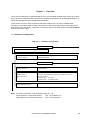
Chapter 1 Overview
The IE-703177-NW-EM is an optional board for an in-circuit emulator as RTE-1000-TP-EE. By connecting the IE-703177-NW-EM to RTE-1000-TP-EE, hardware and software can be debugged efficiently in
system development using the V850E/CG2 CARGATE-F.
In this manual, the basic setup sequences and switch settings of the IE-703177-NW-EM when
connecting it to the RTE-1000-TP-EE are described. For the names and functions of the parts of the
RTE-1000-TP-EE, and for the connection of elements, refer to the RTE-1000-TP-EE User’s Manual
which is a separate volume.
1.1 Hardware Configuration
Figure 1-1:
Hardware Configuration
Optionalsold
hardware
Separately
hardware
In-circuit emulator (RTE-1000-TP-EE)
Optional board
IE-703177-NW-EM
RTE-1000-TP-EE can be used as in-circuit emulator for V850E/CG2 by
adding these boards.
Separately sold hardware
Extension probe
(SWEX-144SD-1 Note )
General-purpose extension probe made by TOKYO ELETECH
CORPORATION.
PC interface board
RTE-PCIF-EE
RTE-PCCIF-EE
These boards are used to connect the RTE-1000-TP-EE to a personal
computer. These boards are inserted in the expansion slot of the
personal computer.
RTE-PCIF-EE : for PCI bus
RTE-PCCIF-EE : for PCMCIA socket
Power adapter
(EB-POWERFW7301/05)
AC adapter dedicated to the NEC’s in-circuit emulator
Note: For further information, contact Daimaru Kogyo Co., Ltd.
Tokyo Electronic Components Division
(TEL +81-3-3820-7112)
Osaka Electronic Components Division
(TEL +81-6-244-6672)
User’s Manual U16583EE1V0UM00
13
Chapter 1
Overview
1.2 Features (When Connected to RTE-1000-TP-EE)
•
Maximum operation frequency: 40 MHz
•
Maximum operating frequency of the oscillator: 4 - 6 MHz
•
Extremely lightweight and compact
•
Higher equivalence with target device can be achieved by omitting buffer between signal cables.
•
Following pins can be masked: RESET, NMI, INTP0-INTP9
•
Following internal signals can be masked: NMI1(FPU), INT0-INT50
•
Two methods of connection to target system:
- Direct connection of the IE-703177-NW-EM
- Attach an extension probe (sold separately) to the connection tab of the IE-703177-NW-EM.
•
Dimensions of the IE-703177-NW-EM are as follows.
Table 1-1:
Dimensions of the IE-703177-NW-EM
Parameter
Value
Power dissipation
4.0 W (at 40-MHz operation frequency)
External dimensions
(Refer to APPENDIX A DIMENSIONS)
Height
35 mm
Length
140 mm
Width
140 mm
Weight
300 g
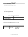
1.3 Function Specifications (When Connected to RTE-1000-TP-EE)
Table 1-2:
Function Specifications
Parameter
Emulation memory capacity
14
Specification
Internal ROM
None
On board emulation
memory
32 bit width: 16 Mbytes (mounted on board in
two banks: 8 MB + 8 MB)
16 bit width: 8 Mbytes (mounted on board in two
banks: 4 MB + 4 MB)
User’s Manual U16583EE1V0UM00
Chapter 1
Overview
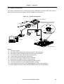
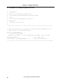
1.4 System Configuration
The system configuration when connecting the IE-703177-NW-EM to the RTE-1000-TP-EE, which is
then connected to a personal computer (PC/AT compatible) is shown below.
Figure 1-2:
System Configuration
<6>
IE-703177-NW-EM
<11>
[Magnified drawing: example of use
of connector for target connection]
<5>
RTE-1000-TP-EE
<10>
N-Wire cable
(for user system
connection)
<4>
<8>
10
8
10
9
FG
SG
<3>
Target
system
CN
4
3
73
<9>
D
-E
2
JA
PA
N
72
S
CN
2
44
37
-1
IN
X
CN
1
MA
DE
E
PA
JA
Ta
rge
t
N
SW
EX
-14
4S
D-1
SG
FG
W
FG
1
T
TES
36
FG
14
4
CN
<7>
T
TE
<1>
<2>
<8>
For PC/AT
<9>
Target System
Remark
<1> Personal computer
<2> PC interface board (RTE-PCIF-EE, RTE-PCCIF-EE: sold separately)
<3> PC interface cable (included with RTE-PCIF-EE or RTE-PCCIF-EE)
<4> In-circuit emulator (RTE-1000-TP-EE: sold separately)
<5> N-Wire cable (included with RTE-1000-TP-EE)
<6> In-circuit emulator option board (IE-703177-NW-EM)
<7> Extension probe (SWEX-144SD-1: sold separately)
<8> Connector for emulator connection (YQPACK144SD: included)
<9> Connector for target connection (NQPACK144SD: included)
<10> Power adapter for RTE-1000-TP-EE (EB-POWERFW7301/05: sold separately)
<11> Power adapter for IE-703177-NW-EM (EB-POWERFW7301/05: sold separately)
User’s Manual U16583EE1V0UM00
15
Chapter 1
Overview
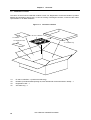
1.5 Contents in Carton
The carton of the IE-703177-NW-EM contains a main unit, Registration Card and a Readme (includes
detailed documentation packing list). In case of missing or damaged contents, contact an NEC sales
representative or an NEC distributor.
Figure 1-3:
Contents in Carton
<1> IE-703177-NW-EM
<4> Readme
<3> Registration Card
<4> Anti static bag
<1>
<2>
<3>
<4>
16
IE-703177-NW-EM × 1 (inside Anti static bag)
Readme (includes detailed packing list, with all attached documents listed in detail) × 1
Registration card × 1
Anti static bag × 1
User’s Manual U16583EE1V0UM00
Chapter 1
Overview
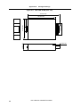
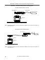
1.6 Connection between RTE-1000-TP-EE and IE-703177-NW-EM
The procedure for connecting the RTE-1000-TP-EE and IE-703177-NW-EM is described below.
<1> Connect the RTE-1000-TP-EE to the CN7 of the IE-703177-NW-EM (refer to Figure 1-4).
Figure 1-4:
Connection between RTE-1000-TP-EE and IE-703177-NW-EM
IE-703177-NW-EM
RTE-1000-TP-EE
N-Wire cable
User’s Manual U16583EE1V0UM00
17
[MEMO]
18
User’s Manual U16583EE1V0UM00
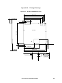
Chapter 2 Name and Function of Components
This chapter describes the names, functions, and switch settings of components comprising the
IE-703177-NW-EM. For the details of the pod, jumper, and switch positions, etc., refer to the
RTE-1000-TP-EE User’s Manual.
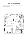
2.1 Component Name and Function of IE-703177-NW-EM
Figure 2-1:
IE-703177-NW-EM (1/2)
(a) Top View
User’s Manual U16583EE1V0UM00
19
Chapter 2 Name and Function of Components
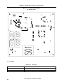
Figure 2-1:
IE-703177-NW-EM (2/2)
(b) Bottom View
(1)
Test pins
Table 2-1:
Test Pins
Test pins
Function
TP3,TP4,TP17,TP18,TP21,TP22
GND
TP19,TP20
GND (optional for SWEX-144SD-1 frame ground & signal ground)
20
User’s Manual U16583EE1V0UM00
Chapter 2 Name and Function of Components
(2)
Connector List
Table 2-2:
Connector List
Connector
Function
CN1
5 V board power supply
CN2,CN3,CN4,CN5,CN6,CN8,CN10
Reserved
CN7
N-Wire connector to RTE-1000-TP-EE
CN9
Emulation Board Mode setting
CN11
Emulation Memory mapping
Jumper on
Connector
Function
Close
Open
CN11 1-2
CS0 mapped
Emulation Memory Bank0 selected Target
CN11 3-4
CS1 mapped
Emulation Memory Bank1 selected Target
CN11 5-6
CS2 mapped
Emulation Memory Bank1 selected Target
CN11 7-8
CS3 mapped
Emulation Memory Bank1 selected Target
CN11 9-10
CS4 mapped
Emulation Memory Bank1 selected Target
CN11 11-12 CS6 mapped
Emulation Memory Bank1 selected Target
CN11 13-14 Reserved
Reserved
Reserved
CN11 15-16 Reserved
Reserved
Reserved
Jumper on
Connector
Function
Close
Open
CN9 1-2
Emulation Mode setting
Stand-alone
Target
CN9 3-4
Emulation RAM mapping
(only required in standalone mode)
Memory Interface configured
16-bit width
Memory Interface configured
32-bit width
CN9 5-6
Reserved
Reserved
Reserved
CN9 7-8
Reserved
Reserved
Reserved
CN9 9-10
Reserved
Reserved
Reserved
CN9 11-12
Reserved
Reserved
Reserved
CN9 13-14
Reserved
Reserved
Reserved
CN9 15-16
Reserved
Reserved
Reserved
User’s Manual U16583EE1V0UM00
21
Chapter 2 Name and Function of Components
(3)
Sockets
Table 2-3:
Sockets
Socket
(4)
Function
SO1
Socket for target connection (optional via probe cable)
SO2
Socket of crystal oscillator module for main clock supply (4 to 6 MHz)
Switches/Buttons
Table 2-4:
Switches
Socket
(5)
Function
SW2
5 V board power supply off/on
SW3
Reserved (Main clock supply factory setting)
SW4
Reserved
SW1
Reset (Only on EM board, not for target hardware)
The SW1 could be masked
LEDs
Table 2-5:
LEDs
LED
22
Function
D4 (yellow)
Indicates detection of valid target mode selection
D5 (yellow)
Indicates detection of valid target power (3.3 V, CVDD and GND)
D9 (red)
Indicates board power supplied 5.0 V
D7 (yellow)
Indicates RESET active
D8 (green)
Indicates 3.3 V target power on
D6 (yellow)
Indicates program execution.
on: Program is executed
off: Program is halted
User’s Manual U16583EE1V0UM00
Chapter 2 Name and Function of Components
(6)
Jumpers
Table 2-6:
Jumper
Function
Jumper List
1-2
2-3
JP1
AVREF
Internal 3.3 V
Target
JP2
AVDD
Internal 3.3 V
Target
JP3
AVSS
Internal GND
Target
Jumper
JP4
Function
N-Wire power detection
Open
Normal operation
User’s Manual U16583EE1V0UM00
Closed
Reserved
23
Chapter 2 Name and Function of Components
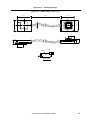
2.2 Clock Setting
2.2.1 Clock Structure
The main clock supply of IE-703177-NW-EM can be provided by an internal crystal oscillator (plugged
on SO2). By default the IE-703177-NW-EM is equipped with a crystal oscillator on socket SO2
(5.000 MHz / 3.3 V).
Using a clock source from target hardware is not possible.
Figure 2-2:
Clock Structure
Main Clock
EVA Chip
FPGA
IE-703177-NW-EM
V850E/CG2
CARGATE-F
I/O Chip
Osc.
SO2
n.c.
n.c.
X1
X2
Target System
24
User’s Manual U16583EE1V0UM00
Chapter 2 Name and Function of Components
2.2.2 Main clock setting
The following clock setting methods are available for main clock supply.
(1)
(2)
Use the crystal oscillator mounted on SO2 of the IE-703177-NW-EM as internal clock
(5.000 MHz).
Change the crystal oscillator mounted on SO2 of the IE-703177-NW-EM and use it as the
internal clock (permitted from 4.000 MHz to 6.000 MHz).
Caution:
When using an different crystal oscillator, use a 3.3 V type.
Table 2-7:
Hardware Configuration for Main Clock Supply
Type of Clock
SO2 Crystal/Ceramic
Resonator
SW3
SW4
(1) Crystal oscillator
mounted on SO2
as internal clock
Factory setting
(5.000 MHz)
Reserved (default factory setting)
Reserved (default factory
setting)
(2) Customer specific
crystal oscillator
mounted on SO2
as the internal clock
Customer specific
(4.000 to 6.000 MHz)
Reserved (default factory setting)
Reserved (default factory
setting)
User’s Manual U16583EE1V0UM00
25
Chapter 2 Name and Function of Components
2.3 Operation Mode
The IE-703177-NW-EM supports only the ROMless mode, the same as the V850E/CG2 CARGATE-F.
For this the following mode setting has to be configured.
2.3.1 When emulator is used as stand-alone unit
When using a debugger, be sure to set Jumper on CN9 1-2 for standalone mode. During this standalone mode, the
(1)
target mode pins are masked and are not evaluated. The LED D4 is switched on.
(2)
target CSx pins are masked and are driving High level on default.
(3)
target RESET pin is masked.
The mode pins on target interface are monitored only. For checking target mode setting, check that D4
LED is on (on == mode correct).
2.3.2 When emulator is connected to target system
When using a debugger, be sure to remove Jumper on CN9 1-2 for target mode. During this mode, the
(1)
on board RESET will stay active, until target power is switched on.
(2)
on board RESET becomes active, when target power will be switched off.
The emulation mode will be set by the target mode pins MODE0, MODE1 and MODE2. For checking
target mode setting, check that D4 LED is on (on == valid correct).
For settings of the mode pins refer to the V850E/CG2 CARGATE-F Hardware User’s Manual.
26
User’s Manual U16583EE1V0UM00
Chapter 3 Factory Settings
Table 3-1:
Item
Factory Settings
Setting
Remark
JP1
1
3
Use internal 5 V for AVREF by default.
JP2
1
3
Use internal 5 V for AVDD by default.
JP3
1
3
Use internal GND for AVSS by default.
1
JP4
CN11
CN9
CN3
CN8
2
Reserved (N-Wire power detection)
2
10
1
9
2
10
1
9
2
10
1
9
2
10
1
9
Emulation RAM mapping
Emulation Memory Bank0 selected by
default. CS0 mapped internal
Emulation Board Mode setting
Standalone selected by default
Memory Interface configured 32-bit width
by default
Reserved
Reserved
SO2
5.000-MHz crystal oscillator is mounted.
The main clock frequency can be changed
by changing the crystal oscillator
(4.000 MHz to 6.000 MHz)
SW3
Initial position
Reserved (Main clock supply factory
setting)
SW4
Initial position
Reserved
User’s Manual U16583EE1V0UM00
27
[MEMO]
28
User’s Manual U16583EE1V0UM00
Chapter 4 Cautions
4.1 Standby Release
In emulation mode the main clock oscillator is always running. Therefore, no oscillation stabilization
time is required when stop mode is released. As a consequence the emulator will wake up immediately
from stop mode while the target device always assures the oscillation stabilization time for main oscillator.
4.2 N-Wire connection speed settings (JTAG)
The emulation board supports the following speed setting for the N-Wire interface to the
RTE-1000-TP-EE:
• > 4.5 MHz Oscillator on SO2 used: 25 MHz JTAG clock (env jtag25)
• < 4.5 MHz Oscillator on SO2 used: 12 MHz JTAG clock (env jtag12)
This setting must be done in the .rc-file (refer to Figure 5-1, “Sample .rc file for Green Hills Multi 2000,”
on page 35) or in the target window of the debugger environment.
4.3 Pin Functions
4.3.1 MODE0 to MODE2 pins
The operation mode of the emulator is ROM-less mode only. When the emulator operates as a standalone unit, the MODE0 to MODE2 pins are not evaluated. When the emulator operates in target-mode,
the MODE0 to MODE2 pins are valid.
The MODE0 to MODE2 pins are connected as follows.
• MODE0: Connected to target connector
• MODE1: Connected to target connector
• MODE2: Connected to target connector
The MODE0 to MODE2 are connected to the FPGA. Therefore the behavior differs from the target
device.
4.3.2 RESET input
The RESET input pin is connected to VDD via a resistor (10 KΩ pull-up to +3,3V). Therefore the behavior differs from the target device.
4.3.3 Clock signals
(1)
X1, X2 signal
The input signals from the target system are not connected. Therefore the input characteristics
may differ from the target device.
User’s Manual U16583EE1V0UM00
29
Chapter 4 Cautions
4.3.4 Port pins
The ports PDH, PCS, PCT, PCD and PCM, which are shared with the memory bus interface function,
are not emulated by the I/O chip, but by the FPGA chip (refer to Figure 4-2, “Configuration of Emulation
Memory,” on page 33).
Driving capabilities are different compared to the target device.
• FPGA:
12 mA
• Target device:
3 mA
Figure 4-1:
Configuration of Ports PDH, PCS, PCT, PCD and PCM
FPGA
Po rt
Bus I/F
Emulation I/F
PCS, PCT,
PCD, PCM,
PDH
A23 to A0
D15 to D0
RAM_CS0, CS1
RAM_RDL/RDH
RAM_WRx
PDH/D31 to D16
CN11 CSx
mapping
Emulation
Memory
Target System
Emulation memory is connected to the lines of A23 to A0, D31 to D16 / PDH and D15 to D0. This produces additional load. Additionally a 33 Ω serial resistor is designed into each Bus I/F line.
The control signals of the emulation memory are supplied from the FPGA and are not shared with the
PCS, PCT, PCD and PCM pins.
30
User’s Manual U16583EE1V0UM00
Chapter 4
Cautions
4.3.5 Bus interface pins
(1)
Address lines A23 to A0
Since emulation memory is connected to the address line A23 to A0, additional load has to be
considered for the target system. Driving capabilities are different compared to the target device.
(2)
• Emulator:
12 mA
• Target device:
3 mA
Data lines D15 to D0
Since emulation memory is connected to the data line D15 to D0, additional load has to be considered for the target system. Driving capabilities are different compared to the target device.
(3)
• Emulator:
12 mA
• Target device:
3 mA
Data lines D31 to D16 / PDH
Since emulation memory is connected to the data line D31 to D16, additional load has to be considered for the target system. Driving capabilities are different compared to the target device.
(4)
• Emulator:
12 mA
• Target device:
3 mA
Control lines RD, WR, WR0, WR1, BEN3 to BEN0
Driving capabilities are different compared to the target device.
(5)
• Emulator:
12 mA
• Target device:
3 mA
Chip select lines CS0, CS1, CS2, CS3, CS4, CS6
All CSn signals can be used for selecting emulation memory or memory on a target system
(n = 0, 1, 2, 3, 4, 6).
The definition is done by the emulation memory configuration, selectable via CN11 Table 2-2,
“Connector List,” on page 21.
As soon as an emulation memory block is assigned to a CSn signal, the signal is reserved for
emulation memory and is not usable by a target system any more. In that case the target system
will see a high-level (3.3 V) on that line. Driving capabilities are different compared to the target
device.
(6)
• Emulator when CSn used for target system:
12 mA
• Target device:
3 mA
WAIT input
The WAIT input is held to high-level (+3.3 V) via a 10 KΩ pull-up resistor. For the emulator working
in stand-alone mode (set by CN9 Table 2-2, “Connector List,” on page 21) this is required. This is
different compared to the target device.
User’s Manual U16583EE1V0UM00
31
Chapter 4 Cautions
4.3.6 Power supply voltage VDD3x
The emulator is supplied by its own power supply. Therefore the target voltage input at the target probe
is only used as a sensing input, and the resulting power consumption may be less as it would be for the
target device.
Nevertheless, when a target hardware is to be used (non stand-alone operation), the emulator needs to
be connected to all power supply lines VDD3x as well as VSS3x.
4.3.7 Clock supply voltage CVDD
The clock supply voltage input CVDD behaves the same as the VDD3x lines (refer to 4.3.6 Power supply
voltage VDD3x).
Nevertheless, when a target hardware is to be used (non stand-alone operation), the emulator needs to
be connected to the clock supply lines CVDD and CVSS.
4.3.8 AVDD, AVREF, AVSS pins
Power supply of to these pins can be connected to the internally 3.3 V power supply by jumpers JP1,
JP2, and JP3 (factory setting). In that case resulting A/D converter values and load on AVDD, AVREF,
AVSS pins may differ.
4.4 BPC register access (setting of programmable peripheral I/O area)
In emulation mode, the read access to the BPC register differs, out of the tow masked bits 12 and 13.
During program execution there is no difference and there is no influence of the function. Recommended setting for CARGATE-F is 8F81h. The read value is BF81h, where bit 12 and 13 must be
ignored.
32
User’s Manual U16583EE1V0UM00
Chapter 4
Cautions
4.5 Emulation Memory
Figure 4-2:
Configuration of Emulation Memory
FPGA
EVA Chip
Po rt
Bus I/F
Emulation I/F
PCS, PCT,
PCD, PCM,
PDH
A23 to A0
D15 to D0
RAM_CS0, CS1
RAM_RDL/RDH
RAM_WRx
CN11 CSx
mapping
V850E/CG2
CARGATE-F
I/O Chip
Emulation
Memory
PDH/D31 to D16
Bank0 8 MB
Bank1 8 MB
Target System
The emulation memory must be configured before downloading a program. For this the CN11 is provided to setup this via FPGA. The emulation memory can be configured to be used as 32-bit or 16-bit
memory. In 16-bit mode, only half the size is available. The mode setting determines the width. Both
banks are configured to the same data width.
Emulation memory is split into two banks of 8 MByte each: bank0 and bank1 (2M × 32 or 2M × 16).
Bank0 can be mapped to CS0 or it can be disabled. Bank1 could be mapped on any of the chip-select
signals CS1, CS2, CS3, CS4 or CS6, or it can be disabled.
The banks can be accessed in 32-bit or 16-bit mode. In standalone mode, this will be done via jumper
setting on CN9 (refer to Table 2-2, “Connector List,” on page 21). In target mode this will be done by the
evaluation of MODE0 to MODE2 pins.
Emulation memory can be accessed with no wait states.
The data lines D32 to D16 can either be used as data lines or as port pins PDH. The ports are available
only in 16-bit memory mode.
Caution:
If the ports PCS, PCT, PCD and PCM are used in port mode, the emulation memory
could still be used. This is different compared to the target device.
User’s Manual U16583EE1V0UM00
33
Chapter 4 Cautions
4.5.1 Emulation memory mapping
Bank0 can be mapped to CS0, bank1 can be mapped to CSn (n = 1, 2, 3, 4 or 6). This will be done via
jumper setting on CN11 (refer to Table 2-2, “Connector List,” on page 21).
Emulation memory can be accessed with zero data wait state, which is specified in the data wait control
register DWC0 or DWC1.
The data lines D31 to D16 / PDH can either be used as address lines or as port pins, depending on the
bus size required. The data lines D31 to D16 must be configured by the mode pins in user mode and
via jumper setting on CN9 (refer to Table 2-2, “Connector List,” on page 21) in standalone mode.
4.6 Emulated Function Blocks
The IE-703177-NW-EM emulator option board is based on a target device, the V850E/CG2
CARGATE-F I/O chip. The following table shows the functions, which are not or not complete emulated
by the I/O chip itself. For these functions a deviation between target device and emulator behavior might
be possible.
Table 4-1:
Functions Emulated by Other Hardware than Real-chip
Emulation
Function
FPGA
External memory interface / Ports (A23 to A0, D31 to D15 / PDH, D15 to D0, PCS,
PCT, PCM, PCD)
Eva Chip D703193
CPU
Eva Chip D703193
IRAM
Eva Chip D703193
iCache
Eva Chip D703193
INTC (Interrupt controller)
Eva Chip D703193
DMA controller
Eva Chip D703193 / FPGA Reset
Eva Chip D703193
Mode pins
4.7 Extension Probe
For best signal quality use the emulator without an extension probe if possible. When necessary use
the SWEX-144SD extension probe. Do not use more than one extension probe in serial.
34
User’s Manual U16583EE1V0UM00
Chapter 5 Debugger Operation
5.1 IRAM initialisation for the EVA chip
The IRAM of the EVA chip must be setup after power on and after each reset. After power on and after
reset, the IRAM is not available and therefore must be configured in the .rc-file, when using Green Hills
Multi 2000, for re-configuration after reset.
If this initialisation has not been implemented, the program execution fails.
5.2 Start-up for Green Hills Multi 2000
A sample .rc-file for Multi 2000 is shown in Figure 5-1.
Figure 5-1: Sample .rc file for Green Hills Multi 2000
//
// CargateF_HW_Test.rc
//
// Start-up file for Cargate-F EM test program
// (C) Copyright by NEC Electronics (Europe) GmbH
//
// Revisions:
// 2002/11/28 ME Initial.
//
**************************************************************************
remote rteserv;
target init;
target env jtag25;
//target env jtag12;
target env 64m romless d0 i2;
//
//
//
//
//
//
target sfrfile.\Src\D3177.800;//
target reset;
//
<CargateEM.rc;
connect to target
reset RTE ICE
set up RTE ICE for main clock >4.5 MHz
set up RTE ICE for main clock <4.5 MHz
set up CPU (64 MB mode, no ROM, no dCache,
2-way iCache)
load SFR definitions from device file
reset CPU
// set up iRAM size (60K mode, only 32K used)
target env !reset !nmi0 !nmi1 nmi2 hldrq stopz;
// unmask/mask target pins
// display opcodes in ASM view
eval $_OPCODE
= 1;
eval $_ASMCACHE = 0;
// setup GUI
button Reset
{target reset; target sfr rsz 0x40;}
button ViewMemory memview 0x00000000;
// indicate success
echo " ";
echo "--------------------";
echo "Initialization done.";
echo " ";
// **************************************************************** EOF ***
User’s Manual U16583EE1V0UM00
35
Chapter 5
Debugger Operation
5.3 CargateEM.rc for setting rsz register after reset.
//
// CargateEM.rc
//
// Macros for Cargate-EM configuration
// (C) Copyright by NEC Electronics (Europe) GmbH
//
// Usage:
// Just include (<CargateEM.rc) this file
//
// Revisions:
// 2003/02/20 ME Initial
//
//
**************************************************************************
// This next section sets some SFRs to the device reset defaults as the
// reset values of the emulator differ.
define CargateEM_SFRFix() {
// setup any other SFRs...
target sfr rsz 0x40; // set up iRAM size (60k mode, only 32k used)
}
CargateEM_SFRFix();
// do it right away
b 0x00000000 { CargateEM_SFRFix(); c; } // and after every reset
// **************************************************************** EOF ***
36
User’s Manual U16583EE1V0UM00
Chapter 6
Limitations
6.1 Emulation Memory
Emulation memory size is limited to 16 MB.
Emulation memory must be selected by a CSn line (n = 0, 1, 2, 3, 4, 6). That CSn line cannot be used
for the target application.
Additional memory can be connected as target memory.
6.2 In-circuit Emulator RTE-1000-TP-EE
The in-circuit emulator option board IE-703177-NW-EM should be operated only with an in-circuit emulator as RTE-1000-TP-EE.
6.3 Software Development Tools
For correct operation in conjunction with the instruction cache it is mandatory to use the latest version
of the following files with the development/debugging tools.
6.3.1 Green Hills Multi 2000 Environment for V800
• Multi 2000
version 3.5.1 or higher (including actual rteserv.exe)
6.3.2 Midas
• RTE4win32
version 5.08 or higher Note
Note: License for RTE target server is required. This license could be ordered separately, if not available.
User’s Manual U16583EE1V0UM00
37
[MEMO]
38
User’s Manual U16583EE1V0UM00
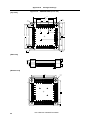
Appendix A
Figure A-1:
Package Drawings
IE-703177-NW-EM (Unit: mm)
128.010±.002
120.390±.002
115.000±.002
103.000±.002
15.000±.002
41.450±.002
9.450±.002
3.400±.002
64.050±.002
95.050±.002
135.000±.002
User’s Manual U16583EE1V0UM00
6.000±.002
4.000±.002
140.000±.002
14.000±.002
3.000±.002
5.000±.002
7.000±.002
5.000±.002
34.400±.002
140.000±.002
Top View
39
Appendix A
Figure A-2:
Package Drawings
RTE-1000-TP-EE (Unit: mm)
185.000±.002
40
120.000±.002
50.000±.002
40.000±.002
26.000±.002
150.000±.002
35.000±.002
User’s Manual U16583EE1V0UM00
Appendix A
SWEX-144SD-1 (Unit: mm)
(55.5)
(55.5)
(295±8)
TET
(Ø 7)
CN1
Target
JAPAN
FG
SG
TET
SWEX-144SD-E2
(47.5)
FG
CN4
SG
144
FG
109
1
108
CN3
SWEX-144SD-1
(47.5)
Figure A-3:
Package Drawings
73
36
37 CN2
72
MADE IN JAPAN
FG
(19.5)
(12.5)
6.4 (12.5)
(19.5)
(24)
(24)
Red
Black
(5)
(45)
Ground Wire
User’s Manual U16583EE1V0UM00
41
Appendix A
Figure A-4:
Package Drawings
NQPACK144SD (Unit: mm)
[Top view]
27.0
0.5
C1.5
0.5 × 35 = 17.5
7.0
3 R1.5
0.3
109
144
108
1
36
26.2
22.65
7.0
18.9
3 φ 1.0
73
72
37
2.5
2.5
20.1
0.18
0.5
0.5
21.05
0.2
1.85
1.2
3.7
9.45
5.5
3.9
[Side view]
[Bottom view]
23.0
12.0
109
144
1
73
36
0.2
20.1
108
72
37
4 φ 2.0 Height of projection1.8
42
User’s Manual U16583EE1V0UM00
Appendix A
Figure A-5:
Package Drawings
YQPACK144SD (Unit: mm)
[Top view]
22.65
0.5 × 35 = 17.5
0.5
C2.0
4 φ 2.2
7.0
109
144
108
1
36
27.0
29.0
19.4
7.0
16.4
23.6
21.2
18.8
3 φ 1.0
73
37
3 R2.5
72
4 R1.5
[Side view]
0.25 × 0.3
1.2
7.4
3.9
3.1
2.2
9.0
1.2
3.7
2.5
0.3
0.25
[Bottom view]
22.8
109
19.6
C1.5
144
108
20.8
1
73
72
37
User’s Manual U16583EE1V0UM00
0.2
36
43
Appendix A
Figure A-6:
Package Drawings
HQPACK144SD (Unit: mm)
[Top view]
22.65 ±0.15
0.5 × 35 = 17.5
±0.1
4 φ 2.2
7.0 ±0.1
C2.0
109
2.75
3.95
144
1
108
27.0
29.0
73
2.75
36
3.95
19.4
7.0
18.4
23.9
16.0
3 φ 1.0
72
37
3 R2.5
4 R1.5
2.3
7.4
1.6
3.9
2.25
3.1
1.2
[Side view]
0.25
[Bottom view]
22.8
C1.5
19.6
109
144
108
21.4±0.2
1
72
44
37
User’s Manual U16583EE1V0UM00
0.2
36
73
Appendix A
Figure A-7:
Package Drawings
YQSOCKET144DN (Unit: mm)
29
5.9
0.5x35=17.5
1.03
0.5
0.3
C2.0
2.7 2.4
4.5
23.6
21.2
18.8
16.4
3.55
0.7
4-Ø1.0
4-Ø2.2
20.5
22.65
User’s Manual U16583EE1V0UM00
45
[MEMO]
46
User’s Manual U16583EE1V0UM00
Appendix B
Example of Use of Connector for Target Connection
Figure B-1: When directly connecting device to target system
(Connector for target connection is not used)
Device
Target system
Figure B-2:
When equipping device by using connector for target connection
Fastening screws
HQPACK144SD
Device
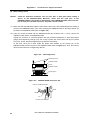
NQPACK144SD
Target system
User’s Manual U16583EE1V0UM00
47
Appendix B
Figure B-3:
Example of Use of Connector for Target Connection
Connection between emulator and target system
(a) When extension probe is not used
Box (optional)
N-Wire cable
IE-703177-NW-EM
RTE-100-TP-EE
Note
YQPACK
NQPACK
Target system
Note: Connector for emulator connection (YQSOCKET144SDN) can be inserted at this position for
height adjustment.
(b) Example of use of extension probe
Box (optional)
IE-703177-NW-EM
N-Wire cable
RTE-100-TP-EE
Note
YQPACK
NQPACK
Target system
Note: Connector for emulator connection (YQSOCKET144SDN) can be inserted at this position for
height adjustment.
48
User’s Manual U16583EE1V0UM00
Appendix C
Connectors for Target Connection
C.1 Use
(1)
When mounting NQPACK144SD to target system
<1> Coat the tip of four projections (points) at the bottom of the NQPACK144SD with two-component
type epoxy adhesive (cure time longer than 30 min.) and bond the NQPACK144SD to the target
system. If not bonded properly, the pad of the printed circuit board may peel off when the emulator
is removed from the target system. If the lead of the NQPACK144SD does not coincide with the
pad of the target system easily, perform step <2> to adjust the position.
<2> To adjust the position, insert the guide pins for position-adjustment (NQGUIDE) provided with
NQPACK144SD into the pin holes at the upper side of NQPACK144SD (refer to Figure C-1).
The diameter of a hole is φ = 1.0 mm. There are three non-through holes (refer to APPENDIX A
DIMENSIONS).
<3> After setting the HQPACK144SD, solder NQPACK144SD to the target system. By following this
sequence, adherence of flux or solder sputtering to contact pins of the NQPACK144SD can be
avoided.
• Recommended soldering condition…Reflow
: 240°C, 20 sec. max.
Partial heating : 240°C, 10 sec. max. (per pin row)
<4> Remove the guide pins.
Figure C-1:
Mounting of NQPACK144SD
HQPACK144SD
Guide pins
(NQGUIDE)
NQPACK144SD
Target system
Remark:
NQPACK144SD:
HQPACK144SD:
Connector for target connection
Cover for device installation
User’s Manual U16583EE1V0UM00
49
Appendix C
(2)
Connectors for Target Connection
When setting device
Caution:
Check for abnormal conditions such as resin burr or bent pins before setting a
device to the NQPACK144SD. Moreover, check that the hold pins of the
HQPACK144SD are not broken or bent before setting HQPACK144SD. If there are broken or bent pins, fix them with a thin, flat plate such as a blade.
<1> Make sure that the NQPACK144SD is clean and the device pins are parallel (flat) before setting a
device to the NQPACK144SD. Then, after mounting the NQPACK144SD to the target board, set
the device and HQPACK144SD (refer to Figure C-2).
<2> Using the screws provided with the HQPACK144SD (four locations: M2 × 6 mm), secure the
HQPACK144SD, device, and NQPACK144SD.
Tighten the screws in a crisscross pattern with the provided screwdriver or driver with torque
gauge (avoid tightening strongly only one screw). Tighten the screws with 0.55 kg⋅f⋅cm (0.054
N⋅m) max. torque. Excessive tightening may diminish conductivity.
At this time, each pin is fixed inside the plastic wall dividers by the contact pin of the
NQPACK144SD and the hold pin of the HQPACK144SD (refer to Figure C-3). Thus, pins cannot
cause a short with pins of neighboring devices.
Figure C-2:
Mounting Device
Fastening screws
HQPACK144SD
Device
NQPACK144SD
Target system
Figure C-3:
NQPACK144SD and Device Pin
Hold pin of HQPACK144SD
Divider
Device
Pin
Contact pin of NQPACK144SD
50
User’s Manual U16583EE1V0UM00
Appendix C
Connectors for Target Connection
C.2 Cautions on Handling Connectors
(1)
When taking connectors out of the case, remove the sponge while holding the main unit.
(2)
When soldering the NQPACK144SD to the target system, cover the HQPACK144SD to protect it
against splashing flux.
• Recommended soldering conditions Reflow
:
Partial heating :
240°C, 20 sec. max.
240°C, 10 sec. max. (per pin row)
(3)
Check for abnormal conditions such as resin burr or bent pins before setting a device to the
NQPACK144SD. Moreover, check that the hold pins of the HQPACK144SD are not broken or bent
before setting HQPACK144SD. If there are broken or bent pins, fix them with a thin, flat plate such
as a blade.
(4)
When securing the YQPACK144SD (connector for emulator connection) or HQPACK144SD to the
NQPACK144SD with screws, tighten the four screws temporarily with the provided screwdriver or
driver with torque gauge, then tighten the screws in a crisscross pattern (with 0.054 N⋅m max.
torque).
Excessive tightening of only one screw may diminish conductivity.
If the conductivity is diminished after screw-tightening, stop tightening, remove the screws and
check whether the NQPACK144SD is stained and make sure the device pins are parallel.
(5)
Device pins do not have high strength. Repeatedly connecting to the NQPACK144SD may cause
pins to bend. When setting a device to the NQPACK144SD, check and adjust bent pins.
User’s Manual U16583EE1V0UM00
51
[MEMO]
52
User’s Manual U16583EE1V0UM00
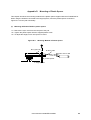
Appendix D
Mounting of Plastic Spacer
This chapter describes the mounting method for the plastic spacer supplied with the IE-V850E-MC-A.
When using the emulator connected to the target system, mount the plastic spacer as shown in
Figure D-1 to fix the pod horizontally.
(1)
Mounting RTE-1000-TP-EE to plastic spacer
<1> Remove the nylon rivet from the rear part of the pod.
<2> Tighten the plastic spacer with the supplied plastic screw.
<3> To adjust the height, use a user spacer or stand.
Figure D-1:
Mounting Method of Plastic Spacer
Box (optional)
N-Wire cable
RTE-100-TP-EE
IE-703177-NW-EM
Plastic spacer
Target system
User’s Manual U16583EE1V0UM00
53
[MEMO]
54
User’s Manual U16583EE1V0UM00
Appendix E
Item
Date published
Document No.
1
February 2003
U16583EE1V0UM00
Revision History
Comment
1st Release
2
3
4
User’s Manual U16583EE1V0UM00
55
[MEMO]
56
User’s Manual U16583EE1V0UM00
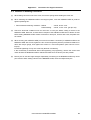
Facsimile Message
From:
Name
Company
Tel.
Although NEC has taken all possible steps
to ensure that the documentation supplied
to our customers is complete, bug free
and up-to-date, we readily accept that
errors may occur. Despite all the care and
precautions we've taken, you may
encounter problems in the documentation.
Please complete this form whenever
you'd like to report errors or suggest
improvements to us.
FAX
Address
Thank you for your kind support.
North America
Hong Kong, Philippines, Oceania
NEC Electronics Inc.
NEC Electronics Hong Kong Ltd.
Corporate Communications Dept. Fax: +852-2886-9022/9044
Fax: +1-800-729-9288
+1-408-588-6130
Korea
Europe
NEC Electronics Hong Kong Ltd.
NEC Electronics (Europe) GmbH
Seoul Branch
Market Communication Dept.
Fax: +82-2-528-4411
Fax: +49-211-6503-274
South America
NEC do Brasil S.A.
Fax: +55-11-6462-6829
Asian Nations except Philippines
NEC Electronics Singapore Pte. Ltd.
Fax: +65-250-3583
Japan
NEC Semiconductor Technical Hotline
Fax: +81- 44-435-9608
Taiwan
NEC Electronics Taiwan Ltd.
Fax: +886-2-2719-5951
I would like to report the following error/make the following suggestion:
Document title:
Document number:
Page number:
If possible, please fax the referenced page or drawing.
Document Rating
Excellent
Good
Acceptable
Poor
Clarity
Technical Accuracy
Organization
CS 01.2