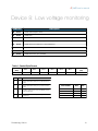
1
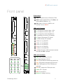
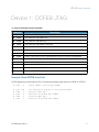
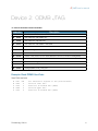
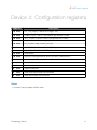
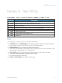
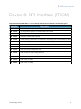
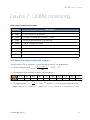
23th January 2014
ODMB user’s manual
Optical DAQ MotherBoard for the ME1/1 stations of the CMS muon endcap detector
Firmware tag: V02-04
ODMB.V2 and ODMB.V3 compatible
Manuel Franco Sevilla, Frank Golf, Guido Magazzù, Tom Danielson, Adam Dishaw, Jack Bradmiiller-Feld
UC Santa Barbara
ODMB user’s manual
Table of Contents
Front panel
2
General
3
3
3
4
Firmware version
VME access through the board discrete “emergency” logic
Jumpers and test points
Device 1: DCFEB JTAG
Example: Read DCFEB UserCode
Device 2: ODMB JTAG
Example: Read ODMB UserCode
Device 3: ODMB/DCFEB control
Bit specification of ODMB_CTRL and DCFEB_CTRL
Information accessible via command “R 3YZC”
Device 4: Configuration registers
Notes
Device 5: Test FIFOs
Notes
5
5
6
6
7
7
8
9
9
10
10
Device 6: BPI Interface (PROM)
11
Device 7: ODMB monitoring
Translation into temperatures and voltages
12
12
Device 8: Low voltage monitoring
13
Device 9: System tests
14
Firmware block diagram
15
i
ODMB user’s manual
Front panel
Push buttons
HRST: Reloads firmware in PROM onto FPGA
SRST: Resets registers/FIFOs in FW. LEDs 1-12
A
blink at different speeds for ~3s
PB1: Sends L1A and L1A_MATCH to all
DCFEBs. Turns on LED 12
LEDs set in firmware
1: 4 Hz signal from clock for data → DDU
3: 2 Hz signal from clock for data → PC
5: 1 Hz signal from internal ODMB clock
ODMB
HRST
7: Data taking: ON normal, OFF pedestal
9: Triggers: ON external, OFF internal
11: Data: ON real, OFF simulated
SRST
2: Bit 0 of L1A_COUNTER
DDU
4: Bit 1 of L1A_COUNTER
PC
B
6: Bit 2 of L1A_COUNTER
8: Bit 3 of L1A_COUNTER
10: Bit 4 of L1A_COUNTER
12: Briefly ON when a VME command is received.
Also ON when PB1 is pressed
LOCK
ERR
DDU
LEDs set in hardware
DDU: Signal Detected on DDU RX
PC: Signal Detected on PC RX
5.0V
1.0V
LVMB FPGA
1.2V
FPGA
1.8V
2.5V
FPGA FPGA
3.3V
FPGA
EJD: JTAG enable for discrete logic (active low)
PC
ETD: DTACK enable for discrete logic (active low)
DON: DONE signal from FPGA. ON when pro-
3.3V
OTX
3.3V
ORX
3.3V
ORX1
grammed
5.0V
VME
3.3V
VME
3.3V
PPIB
LOCK: QPLL is locked
INIT: INIT_B signal from FPGA (active low)
ERR: Error with QPLL
Bottom 12: Voltage monitoring
Firmware tag: V02-04
2
ODMB user’s manual
General
Firmware version
For a given firmware tag VXY-ZK:
❖
❖
Usercode is XYZKdbdb
Firmware version read via “R 4200” is XYZK
VME access through the board discrete “emergency” logic
The FPGA may be accessed via JTAG through the discrete logic as follows
❖
❖
❖
The VME address is 0xFFFC
The bit 0 of the data sent is TMS
The bit 1 of the data sent is TDI
For example, to read the Usercode, starting from JTAG idle (five TMS = 1 & one TMS = 0), the commands are:
W
W
W
W
FFFC
FFFC
FFFC
FFFC
1
1
0
0
To
To
To
To
Select-DR-Scan
Select-IR-Scan
Capture-IR
Shift-IR
W
W
W
W
W
W
W
W
W
W
FFFC
FFFC
FFFC
FFFC
FFFC
FFFC
FFFC
FFFC
FFFC
FFFC
0
0
0
2
0
0
2
2
2
3
Shifting
Shifting
Shifting
Shifting
Shifting
Shifting
Shifting
Shifting
Shifting
Shifting
W
W
W
W
FFFC
FFFC
FFFC
FFFC
1
0
1
0
To
To
To
To
W
R
FFFC
FFFC
0
0
Shifting DR
Shifting DR (Read bit 0 of UserCode)
IR (Read UserCode IR = 3C8)
IR
IR
IR
IR
IR
IR
IR
IR
IR and to Exit1-IR
Update-IR
Run_Test/Idle
Select-DR-Scan
Capture-DR
Since the Usercode register is 32 bits, the last two commands should be repeated 31 more times.
Firmware tag: V02-04
3
ODMB user’s manual
Jumpers and test points
Place the jumpers marked in red in the diagram. The signals sent to the test points marked in blue are:
TP12 RAW_LCT(1)
TP13 L1A_MATCH(1)
TP30 Defined by TP_SEL
TP31
TP14 RAW_LCT(2)
TP15 L1A_MATCH(2)
TP32
TP33
TP16 RAW_LCT(3)
TP17 L1A_MATCH(3)
TP34 Defined by TP_SEL
TP35
TP18 RAW_LCT(4)
TP19 L1A_MATCH(4)
TP36
TP37
TP20 RAW_LCT(5)
TP21 L1A_MATCH(5)
TP38 Defined by TP_SEL
TP39
TP22 RAW_LCT(6)
TP23 L1A_MATCH(6)
TP40
TP41
TP24 RAW_LCT(7)
TP25 L1A_MATCH(7)
TP42
TP43
TP26 L1A
TP27 DDU_DATA_VALID
TP44
TP45
TP28 OTMBDAV
TP29 ALCTDAV
TP46 DCFEB_TDI
TP47 2.5V
TP48 DCFEB_TMS
TP49 Defined by TP_SEL
XILINX
VIRTEX-6
XC6VLX130T
FFG1156
Firmware tag: V02-04
4
ODMB user’s manual
Device 1: DCFEB JTAG
“Y” refers to the number of bits to be shifted
Instruction
Description
W
1Y00
Shift Data; no TMS header; no TMS tailer
W
1Y04
Shift Data with TMS header only
W
1Y08
Shift Data with TMS tailer only
W
1Y0C
Shift Data with TMS header & TMS tailer
R
1014
Read TDO register
W
1018
Resets JTAG protocol to IDLE state (data sent with this command is disregarded)
W
1Y1C
Shift Instruction register
W
1020
Select DCFEB, one bit per DCFEB
R
1024
Read which DCFEB is selected
Example: Read DCFEB UserCode
DCFEB registers are set and read via JTAG. The following procedure reads the 32-bit USERID of DCFEB 3:
W
1020
4
W
W
R
W
R
191c
1F04
1014
1F08
1014
3C8
0
0
0
0
Firmware tag: V02-04
Select DCFEB 3 (one bit per DCFEB)
Set instruction register to 3C8 (read UserCode)
Shift 16 lower bits
Read last 16 shifted bits (DBDB)
Shift 16 upper bits
Read last 16 shifted bits (XYZK)
5
ODMB user’s manual
Device 2: ODMB JTAG
“Y” refers to the number of bits to be shifted
Instruction
Description
W
2Y00
Shift Data; no TMS header; no TMS tailer
W
2Y04
Shift Data with TMS header only
W
2Y08
Shift Data with TMS tailer only
W
2Y0C
Shift Data with TMS header & TMS tailer
R
2014
Read TDO register
W
2018
Resets JTAG protocol to IDLE state (data sent with this command is disregarded)
W
2Y1C
Shift Instruction register
W
2020
Change polarity of V6_JTAG_SEL
Example: Read ODMB UserCode
Read FPGA UserCode:
W
W
R
W
R
291c
2F04
2014
2F08
2014
3C8
0
0
0
0
Firmware tag: V02-04
Set instruction register to 3C8 (read UserCode)
Shift 16 lower bits
Read last 16 shifted bits (DBDB)
Shift 16 upper bits
Read last 16 shifted bits (XYZK)
6
ODMB user’s manual
Device 3: ODMB/DCFEB control
Instruction
Description
W/R 3000
ODMB_CTRL register
W/R 3010
DCFEB_CTRL register
W/R 3020
TP_SEL register (selects which signals are sent to TP27, TP28, TP41, TP42)
W/R 3100
LOOPBACK: 0 → no loopback, 1 or 2 → internal loopback
W/R 3110
DIFFCTRL (TX voltage swing): 0 → minimum ~100 mV, F → maximum ~1100mV
R
3120
Read DONE bits from DCFEBs (7 bits)
R
3124
Read if QPLL is locked
R
3YZC
Read ODMB_DATA corresponding to selection YZ (see below)
Bit specification of ODMB_CTRL and DCFEB_CTRL
‣
‣
‣
‣
‣
‣
‣
‣
‣
‣
‣
‣
‣
‣
‣
‣
‣
‣
‣
ODMB_CTRL[3:0] - Selects CAL_TRGEN (calibration mode).
ODMB_CTRL[4] - Selects CAL_MODE (calibration mode).
ODMB_CTRL[5] - Selects CAL_TRGSEL (calibration mode).
ODMB_CTRL[7] - Selects DCFEB data path: 0 → real data, 1 → dummy data.
ODMB_CTRL[8] - Resets FPGA registers/FIFOs and LEDs 1-12 blink for ~3s. Bit is auto-reset.
ODMB_CTRL[9] - Selects L1A and LCTs: 0 → from CCB, 1 → internally generated.
ODMB_CTRL[10] - Selects LVMB: 0 → real LVMB, 1 → dummy LVMB.
ODMB_CTRL[11] - Kills L1A.
ODMB_CTRL[12] - Kills L1A_MATCH.
ODMB_CTRL[13] - 0 → normal, 1 → pedestal (L1A_MATCHes sent to DCFEBs for each L1A).
ODMB_CTRL[14] - 0 → normal, 1 → pedestal (OTMB data requested for each L1A, needs spec. OTMB FW).
DCFEB_CTRL[0] - Reprograms the DCFEBs. Bit is auto-reset.
DCFEB_CTRL[1] - Resynchronizes the L1A_COUNTER of ODMB and DCFEBs. Bit is auto-reset.
DCFEB_CTRL[2] - Sends INJPLS signal to DCFEBs. Bit is auto-reset.
DCFEB_CTRL[3] - Sends EXTPLS signal to DCFEBs. Bit is auto-reset.
DCFEB_CTRL[4] - Sends test L1A and L1A_MATCH to all DCFEBs. Bit is auto-reset.
DCFEB_CTRL[5] - Sends LCT request to OTMB. Bit is auto-reset.
DCFEB_CTRL[6] - Sends external trigger request to OTMB. Bit is auto-reset.
DCFEB_CTRL[7] - Resets the optical transceivers. Bit is auto-reset.
Firmware tag: V02-04
7
ODMB user’s manual
Information accessible via command “R
‣
‣
‣
‣
‣
‣
‣
‣
‣
‣
‣
‣
‣
3YZC”
YZ = 3F: Least significant 16 bits of L1A_COUNTER
YZ = 21-29: Number of L1A_MATCHes for given DCFEB, OTMB, ALCT
YZ = 31-37: Gap (in number of bunch crossings) between the last LCT and L1A for given DCFEB
YZ = 38: Gap (in number of bunch crossings) between the last L1A and OTMBDAV
YZ = 39: Gap (in number of bunch crossings) between the last L1A and ALCTDAV
YZ = 41-49: Number of packets stored for given DCFEB, TMB, or ALCT
YZ = 4A: Number of packets sent to the DDU
YZ = 4B: Number of packets sent to the PC
YZ = 51-59: Number of packets shipped to DDU and PC for given DCFEB, TMB, or ALCT
YZ = 61-67: Number of data packets received with good CRC for given DCFEB
YZ = 71-77: Number of LCTs for given DCFEB
YZ = 78: Number of available OTMB packets
YZ = 79: Number of available ALCT packets
YZ = 5A: Read last CCB_CMD[5:0} + EVTRST + BXRST strobed
‣ YZ = 5B: Read last CCB_DATA[7:0} strobed
‣ YZ = 5C: Read toggled CCB_CAL[2:0] + CCB_BX0 + CCB_BXRST + CCB_L1ARST + CCB_L1A +
‣
‣
CCB_CLKEN + CCB_EVTRST + CCB_CMD_STROBE + CCB_DATA_STROBE
YZ = 5D: Read toggled CCB_RSV signals
Firmware tag: V02-04
8
ODMB user’s manual
Device 4: Configuration registers
Instruction
Description
W/R 4000
LCT_L1A_DLY[5:0] → Set to LCT/L1A gap - 100
W/R 4004
OTMB_DLY[5:0] → Set to L1A/OTMBDAV gap read with “R 338C”
W/R 400C
ALCT_DLY[5:0] → Set to L1A/ALCTDAV gap read with “R 339C”
W/R 4010
INJ_DLY[4:0] - Delay: 12.5*INJ_DLY [ns]
W/R 4014
EXT_DLY[4:0] - Delay: 12.5*EXT_DLY [ns]
W/R 4018
CALLCT_DLY[3:0] - Delay: 25*CALLCT_DLY [ns]
W/R 401C
KILL[9:1] (ALCT + TMB + 7 DCFEBs)
W/R 4020
CRATEID[6:0]
W/R 4028
Number of words generated by dummy DCFEBs, OTMB, and ALCT
R
4100
Read ODMB unique ID
R
4200
Read firmware version
R
4300
Read firmware build
R
4400
Read month/day firmware was synthesized
R
4500
Read year firmware was synthesized
Notes
1. If unique ID not set, request UCSB to write it.
Firmware tag: V02-04
9
ODMB user’s manual
Device 5: Test FIFOs
Z refers to FIFO: 1 → PC TX, 2 → PC RX, 3 → DDU TX, 4 → DDU RX, 5 → OTMB, 6 → ALCT
Instruction
Description
R
5000
Read one word of selected DCFEB FIFO
R
500C
Read numbers of words stored in selected DCFEB FIFO
W/R 5010
Select DCFEB FIFO
W
5020
Reset DCFEB FIFOs (7 bits, one per FIFO, which are auto-reset)
R
5Z00
Read one word of FIFO
R
5Z0C
Read numbers of words stored in FIFO
W
5Z20
Reset FIFO
Notes
1. All these FIFOs can hold a maximum of 2,000 18-bit words (36 kb)
2. The OTMB, ALCT, and 7 DCFEB FIFOs store the data as it arrives in parallel to the standard data path
• They can hold a maximum of 3 OTMB, 4 ALCT, and 2 DCFEB data packets
3. The DDU TX FIFO stores DDU packets just before being transmitted
• They include the DDU header (4 words starting with 9, 4 starting with A), ALCT data, TMB data, DCFEB
data, and trailer (4 words starting with F, 4 starting with E)
4. The PC TX FIFO stores DDU packets wrapped in ethernet frames just before being transmitted
• They include the ethernet header (4 words) and trailer (4 words)
• They need to be at least 32 words long
5. The DDU and PC RX FIFOs can be used for loopback tests
Firmware tag: V02-04
10
ODMB user’s manual
Device 6: BPI Interface (PROM)
Important: Instruction 6000 takes ~1 second, during which Device 4 and 6 write commands are ignored
Instruction
Description
W
6000
Write configuration registers to PROM
W
6004
Set configuration registers to retrieved values from PROM
W
6020
Reset BPI interface state machines
W
6024
Disable parsing commands in command FIFO while filling FIFO with commands (no data)
W
6028
Enable parsing commands in the command FIFO (no data)
W
602C
Write one word to command FIFO
R
6030
Read one word from read-back FIFO
R
6034
Read number of words in read-back FIFO
R
6038
Read BPI Interface Status Register
R
603C
Read Timer (16 LSBs)
R
6040
Read Timer (16 MSBs)
Firmware tag: V02-04
11
ODMB user’s manual
Device 7: ODMB monitoring
Reads output of the ADC inside the FPGA
Instruction
Description
R
7000
FPGA temperature
R
7100
LV_P3V3: input to FPGA regulators
R
7110
P5V: input to PPIB regulator and level for 5V chips
R
7120
THERM2: board temperature at the center-top
R
7130
P3V6_PP: voltage level for PPIB
R
7140
P2V5: voltage level for FPGA and 2.5V chips
R
7150
THERM1: board temperature close to the LVMB connector
R
7160
P1V0: voltage level for FPGA
R
7170
P5V_LVMB: voltage level for LVMB
Translation into temperatures and voltages
The output of the 7YZ0 commands is a 12-bit number that we call RYZ. The measurement is:
• The FPGA temperature is
TFPGA =
R00 ⇥ 503.975
4096
273.15 [ C]
• The temperature of the thermistors THERM1, THERM2 is given by
RXY
377
455
55A
687
7DD
959
AF8
CB5
E87
FFF
T [° C]
15
20
25
30
35
40
45
50
55
60
• The voltage levels are VYZ =
RYZ
⇥ VYZ,Nom [V] , where VYZ, Nom is the nominal voltage level for that
2048
register. That is, V10, Nom = 3.3V, V13, Nom = 3.6V, V11, Nom = V17, Nom = 5V, V14, Nom = 2.5V, and V16, Nom = 1V.
Firmware tag: V02-04
12
ODMB user’s manual
Mul
Device 8: Low voltage monitoring
Table 1. Control-Byte Format
Instruction
W
Description
Send control byte to ADC
8000
R 8004
Read ADC
Multirange,
+5V, 8-Channel,
Serial 12-Bit ADCs
8010
Select DCFEBs/ALCT to be powered on (8 bits,
R
8018
Read which DCFEBs/ALCT are powered on
BIT 4
BIT 3
SEL0
RNG
BIT 2
W
8020
R
8024
BIP
BIT 0
(LSB)
BIT 1
Select ADC to be read, 0 to 6
PD1
PD0
Read which ADC is to be read
lect the desired “on” channel (Table 2).
BIT 7
BIT 6
START
BIT 5
SEL2
BIT 4
BIT
SEL1
SEL0
RNG
CH0
NAME
PD1
PD0
7 (MSB)
06, 5, 4 0
CH1
CH2
3
0
CH3
2
1
CH5
CH6
—
SEL2
SEL1
SEL0
CHANNEL
0
0
0
CH0
1
CH1
—
-VREF x 1.2207
-VREF x 2.4414
HE MAX1271
Negative
FULL SCALE
—
—
0
1
0
CH2
0
1
1
CH3
1
1
1
NAME
START
First logic 1 after CS goes low defi
These 3 bits select the desired “on
3
RNG
Selects the full-scale input voltage
2
BIP
Selects the unipolar or bipolar con
1, 0 (LSB)
PD1, PD0
Select clock and power-down mod
0
1
0
CH2
0
1
1
CH3
0
BIT 0
1(LSB)
0
PD0
1
CH4
1
BIT 12
0
BIT01
1
BIP
1
1
PD1
1
CH5
CH6
CH7
DESCRIPTION
PD1, PD0power-down
Select clock
and
power-down
modes (Table 4).
Standby
mode
(STBYPD),
clock
mode unaffected.
0
1
BIT
7 (MSB)
RNG operation
Selects
the full-scale
input voltage
Normal
(always
on), external
clock range (Table 3).
INPUT RANGE
mode.
BIP
Selects the unipolar or bipolar conversion mode (Table 3).
1
ection for MAX1270/MAX1271
0
0
Negative
FULL SCALE
SEL0
Table 3. Range and Polarity Selection for MA
Full power-down mode (FULLPD), clock mode
HE MAX1270
SEL1
Normal
operation (always on), internal clock
SEL2,
SEL1,
These 3 bits select the desired “on” channel (TableRANGE
2).
AND POLARITY SELECTION FOR THE MAX1270
mode.
SEL0
1
Table
2. 1Channel
Selection
unaffected.
CH7
SEL2
MODE
First logic
1 after CS goes low defines the beginning of the control byte.
START
1, 0 (LSB)
CH4
START
Table 2. Channel Selection
BIT 3
Table 4. Power-Down and Clock Selection
CHANNEL
BIT 4
MAX1270/MAX1271
Format
polar or bipolar conversion mode (Table 3).
d power-down modes (Table
4).
(MSB)
BIT 5
SEL0
CHANNEL
Multirange,SEL2
+5V,SEL1
8-Channel,
0
0
0
CH0
Serial
12-Bit
ADCs
0
0
1
CH1
DESCRIPTION
er CS goes low defines the beginning of the control byte.
scale input voltage range
(Table
Table
1. 3).
Control-Byte
BIT 6
SEL2, SEL1,
6, 5, 4
ALCT + 7 DCFEBs)SEL0
MAX1270/MAX1271
W
BIT 7
(MSB)
ZERO
0
SCALE (V)
0
0
0
FULL SCALE
CH4
0
0
1
1
0
1
1
CH5
PD1
CH7
0 to +5V
0
0
0 to +10V
1
0
±5V
0
1
0
0
1
1
0
Normal operation (always on), internal clock
INPUT RANGE
RNG
BIP
mode.
Normal
0 to operation
VREF/2 (always on),
0 external clock
0
mode.
0 to VREF
1
0
Standby
power-down
mode 0(STBYPD), clock
±VREF
/2
1
mode unaffected.
±VREF
1
1
Full power-down mode (FULLPD), clock mode
unaffected.
0
1
VREF x 2.4414
0
0 to +5V 0
—
-VREF x 1.2207
-VREF x 2.4414
Negative
FULL SCALE
—
—
-VREF/2
-VREF
_____________________________________
Firmware
tag:ZERO
V02-04 SELECTION FOR THE MAX1270
RANGE AND
POLARITY
INPUT RANGE
—
VREF x 1.2207
Table 3. Range and Polarity Selection for MAX1270/MAX1271
SCALE (V)
Negative
FULL SCALE
PD0RANGE AND POLARITY
MODE
SELECTION FOR THE MAX1271
0
1
VREF x 2.4414
BIP
Table 4. Power-Down
and Clock
±10V
1 Selection
1
VREF x 1.2207
CH6
RNG
FULL SCALE
RNG
BIP
0
0
Negative
VREF/2FULL SCALE
VREF
—
13
ZERO
SCALE (V)
FULL SCALE
0
VREF x 1.2207
ODMB user’s manual
Device 9: System tests
Instruction
Description
W
9000
Test the DDU TX/RX with a given number of PRBS 27-1 sequences
R
900C
Read number of errors during last DDU PRBS test
W
9100
Test the PC TX/RX with a given number of PRBS 27-1 sequences
R
910C
Read number of errors during last PC PRBS test
W
9200
Check N*10000 bits from the PRBS pattern sent by the DCFEB
W/R 9204
Select DCFEB fiber to perform PRBS test
R
9208
Read number of error edges during last DCFEB PRBS test
R
920C
Read number of bit errors during last DCFEB PRBS test
W/R 9300
Set PRBS type for DCFEB: 1 → PRBS-7, 2 → PRBS-15, 3 → PRBS-23, 4 → PRBS-31
W
9400
Check N*10000 bits from the PRBS pattern sent by the OTMB
R
9404
Read number of enables sent by the OTMB
R
9408
Read number of good 10000 bits sent by the OTMB
R
940C
Read number of bit errors during last OTMB PRBS test
W
9410
Reset number of errors in OTMB counter
Firmware tag: V02-04
14
ODMB user’s manual
Firmware block diagram
The firmware can be downloaded from http://github.com/odmb/odmb_ucsb_v2
ODMB_UCSB_V2!–!Top!of!the!design/FPGA!
Control!
Data!
ODMB_VME!W!MBV!
LVMB_MUX!
Dummy!LVMB!
SYSTEM_MON!–!Device!7!
BPI_PORT–!Device!6!
TEST!FIFOs!
DCFEB_V6!!
Dummy!DCFEBs!
TESTFIFOS!–!Device!5!
VMECONFREGS!–!Device!4!
VMEMON!–!Device!3!
DCFEBs!
DMB_RECEIVER!
RX!for!DCFEBs!
ODMBJTAG!–!Device!2!
COMMAND!–!VME!protocol!
LVDBMON!–!Device!8!
LVMB2!
VME!
!
!
CFEBJTAG!–!Device!1!
OTMB!
ODMB_CTRL!W!MBC!
ALCT_TMB_DATA_GEN!!
Dummy!ALCT/OTMB!
DATA!FIFOs!
GIGALINK_DDU!
TX/RX!for!DDU!
PC!
GIGALINK_PC!
TX/RX!for!PC!
CCB!
TRGCNTRL!–!Trigger!control!
OTMB!
CAFIFO!–!Event!manager!
CONTROL!–!DDU!packets!
PCFIFO!–!PC!packets!
!
!
DDU!
CALIBTRG!–!Calibra<on!
Firmware tag: V02-04
15