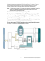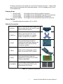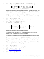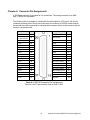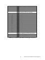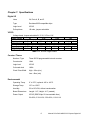
1
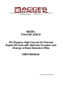
10623 Roselle Street, San Diego, CA 92121 (858) 550-9559 [email protected] www.accesio.com Fax (858) 550-7322 MODEL PCIe-DIO-24DCS PCI Express High-Current 24 Channel Digital I/O Card with Optional Counters and Change of State Detection IRQs USER MANUAL File: MPCIe-DIO-24DCS.D1b Notice The information in this document is provided for reference only. ACCES does not assume any liability arising out of the application or use of the information or products described herein. This document may contain or reference information and products protected by copyrights or patents and does not convey any license under the patent rights of ACCES, nor the rights of others. IBM PC, PC/XT, and PC/AT are registered trademarks of the International Business Machines Corporation. Copyright by ACCES I/O Products, Inc. 10623 Roselle Street, San Diego, CA 92121. All rights reserved. WARNING!! ALWAYS CONNECT AND DISCONNECT YOUR FIELD CABLING WITH THE COMPUTER POWER OFF. ALWAYS TURN COMPUTER POWER OFF BEFORE INSTALLING A BOARD. CONNECTING AND DISCONNECTING CABLES, OR INSTALLING BOARDS INTO A SYSTEM WITH THE COMPUTER OR FIELD POWER ON MAY CAUSE DAMAGE TO THE I/O BOARD AND WILL VOID ALL WARRANTIES, IMPLIED OR EXPRESSED. 2 Manual PCIe-DIO-24DCS PCI Express Digital I/O Warranty Prior to shipment, ACCES equipment is thoroughly inspected and tested to applicable specifications. However, should equipment failure occur, ACCES assures its customers that prompt service and support will be available. All equipment originally manufactured by ACCES which is found to be defective will be repaired or replaced subject to the following considerations. Terms and Conditions If a unit is suspected of failure, contact ACCES' Customer Service department. Be prepared to give the unit model number, serial number, and a description of the failure symptom(s). We may suggest some simple tests to confirm the failure. We will assign a Return Material Authorization (RMA) number which must appear on the outer label of the return package. All units/components should be properly packed for handling and returned with freight prepaid to the ACCES designated Service Center, and will be returned to the customer's/user's site freight prepaid and invoiced. Coverage First Three Years: Returned unit/part will be repaired and/or replaced at ACCES option with no charge for labor or parts not excluded by warranty. Warranty commences with equipment shipment. Following Years: Throughout your equipment's lifetime, ACCES stands ready to provide on-site or in-plant service at reasonable rates similar to those of other manufacturers in the industry. Equipment Not Manufactured by ACCES Equipment provided but not manufactured by ACCES is warranted and will be repaired according to the terms and conditions of the respective equipment manufacturer's warranty. General Under this Warranty, liability of ACCES is limited to replacing, repairing or issuing credit (at ACCES discretion) for any products which are proved to be defective during the warranty period. In no case is ACCES liable for consequential or special damage arriving from use or misuse of our product. The customer is responsible for all charges caused by modifications or additions to ACCES equipment not approved in writing by ACCES or, if in ACCES opinion the equipment has been subjected to abnormal use. "Abnormal use" for purposes of this warranty is defined as any use to which the equipment is exposed other than that use specified or intended as evidenced by purchase or sales representation. Other than the above, no other warranty, expressed or implied, shall apply to any and all such equipment furnished or sold by ACCES. 3 Manual PCIe-DIO-24DCS PCI Express Digital I/O TABLE OF CONTENTS Chapter 1: Introduction ........................................................................................................................................ 5 Features ............................................................................................................................................................. 5 Applications ....................................................................................................................................................... 5 Functional Description ..................................................................................................................................... 5 Figure 1-1: Block Diagram ............................................................................................................................... 6 Ordering Guide .................................................................................................................................................. 7 Factory Options ................................................................................................................................................. 7 Table 1-1: Optional Accessories ..................................................................................................................... 7 Chapter 2: Installation .......................................................................................................................................... 8 Software CD Installation ................................................................................................................................... 8 Hardware Installation ........................................................................................................................................ 8 Chapter 3: Hardware Details ................................................................................................................................ 9 Option Selections .............................................................................................................................................. 9 VCCIO ............................................................................................................................................................. 9 Figure 3-1: Option Selection Map.................................................................................................................... 9 VCCIO Resettable Fused Outputs ................................................................................................................... 9 Pull-Up / Pull-Down Resistor Configuration ................................................................................................... 9 Chapter 4: Address Selection ........................................................................................................................... 10 Chapter 5: Programming ................................................................................................................................... 11 Table 5-1: Register Address Map.................................................................................................................. 11 Table 5-2: Base +0, Port A DIO .................................................................................................................... 12 Table 5-3: Base +1, Port B DIO .................................................................................................................... 12 Table 5-4: Base +2, Port C DIO .................................................................................................................... 12 Table 5-5: Base +3, DIO Port Direction Control Register ............................................................................. 13 Table 5-6: Base +B, DIO COS IRQ Enable................................................................................................... 14 Table 5-7: Base +E, Port C3/CTR-A2 IRQ Enable ....................................................................................... 14 Chapter 6: Connector Pin Assignments........................................................................................................... 15 Table 6-1: DB37M Connector Pin Assignments ............................................................................................ 15 Table 6-2: I/O Connector Signal Names, Directions and Descriptions ......................................................... 16 Chapter 7: Specifications .................................................................................................................................. 17 Table 7-1: VCCIO Logic Levels ..................................................................................................................... 17 Chapter 8: 8254 Counter/Timer ......................................................................................................................... 18 Operational Modes .......................................................................................................................................... 18 Counter/Timer Registers ................................................................................................................................ 19 Programming the 8254 ................................................................................................................................... 19 Reading and Loading the Counters .............................................................................................................. 20 8254 Driver ....................................................................................................................................................... 22 Frequency Measure ..................................................................................................................................... 22 Event Counter .............................................................................................................................................. 22 Generate Frequency .................................................................................................................................... 22 Pulse Width .................................................................................................................................................. 22 Customer Comments ......................................................................................................................................... 23 4 Manual PCIe-DIO-24DCS PCI Express Digital I/O Chapter 1: Introduction The PCIe-DIO-24DCS is a x1 lane PCI Express (PCIe) board designed for use in a variety of Digital I/O (DIO) applications. It uses the high speed PCIe bus to transfer digital data to and from the board. The DIO emulates 8255 compatible chips making it easy to program. This also allows for simple migration from older ACCES’ PCI-based DIO boards. Optional Change of State (COS) detection versions and IRQ capabilities relieve software from constant polling routines that consume valuable processing time. This board is also available in a version that includes three 82C54 Counter/Timers. Lastly, the x1 lane PCIe connector is very flexible and can be inserted into any x1, x4, x8, x16, or x32 PCIe slots. Features 24 high-current DIO lines Three optional 82C54 Counter/Timers IRQ generation from Port C bit 3, Counter A2 (“C” models) or Change of State Detection (“S” models) DIO lines buffered Four and eight bit ports independently selectable for inputs or outputs Jumper selectable 10k ohm Pull-up/Pull-down resistors on DIO lines Jumper selectable VCCIO (5V, 3.3V, 2.5V, 1.8V) VCCIO voltage available to the user via resettable fuses (.5A, .5A, .2A, .1A) Applications Automatic test systems Laboratory automation Robotics Machine control Security systems, energy management Relay monitoring and control Parallel data transfer to PC Sensing switch closures or TTL, DTL, CMOS logic Driving indicator lights or recorders Functional Description This product is a x1 lane PCIe DIO board available in four models ranging from basic DIO to advanced change of state detection and Counter/Timer capabilities. The card emulates an 8255 compatible chip, providing 24 DIO lines. The DIO lines are grouped into three 8-bit ports: A, B, and C. Each 8-bit port is configured via software to function as either inputs or outputs. Port C can be further broken into two 4-bit nybbles via software and configured as either inputs or outputs. Each DIO line is buffered and capable of up to 32mA source/sink. The VCCIO logic level is globally configured via jumper selection as 5V, 3.3V, 2.5V or 1.8V. Also, ports A, B, C low nybble, and C high nybble are individually jumper selected as pull-up or pull-down through 10kΩ resistor networks. The board is shipped factory default as pulled-up. 5 Manual PCIe-DIO-24DCS PCI Express Digital I/O Optionally, the board can include three 82C54 Counter/Timers (“C” versions). They are factory configured and optimized for use with the provided software driver as event counters, frequency output, pulse width outputs, and frequency measurements. Note: “C” Models do not include VCCIO output on the connector as standard. Contact the factory if your application requires this output at DB37M pin 20 in lieu of the frequency output of the third 82C54 chip. This board has three available methods for generating an IRQ. The first method is called COS IRQ ('S' models). COS IRQ works by generating an IRQ when a bit's state changes from low-to-high or high-to-low. COS is enabled/disabled by software on a port-wide basis (A, B, C HI, C LOW). For example, if COS is enabled for Port A, any change on bits A0-A7 will generate an IRQ. The second method, called C3 IRQ, functions by causing an IRQ when a rising signal edge is detected on Port C, bit 3. C3 IRQ is enabled/disabled by software. The last method, named CTR IRQ (‘C’ models), uses the output of Counter A2 to generate an IRQ. When enabled, CTR IRQ will generate an IRQ on a rising signal edge of Counter A2's output. CTR IRQ is also enabled/disabled by software. Figure 1-1: Block Diagram 6 Manual PCIe-DIO-24DCS PCI Express Digital I/O I/O wiring connections for this board are via a male 37-pin D-sub connector. A ribbon cable can be used to connect this card to termination panels. VCCIO is available on pin 20 via a 0.5A resettable fuse. Ordering Guide PCIe-DIO-24D PCIe-DIO-24DC PCIe-DIO-24DS PCIe-DIO-24DCS 24-bit Digital I/O card with 37-pin Male D connector 24-bit Digital I/O card with DB37M, three 82C54 counter/timers 24-bit Digital I/O card with DB37M and COS detection 24-bit Digital I/O card with DB37M, three 82C54’s and COS Factory Options Extended temperature operation (-40° to +85°C) Optional Accessories ADAP37 DB37F screw terminal board, lowest cost solution plugs directly onto the DIO card’s bracket mounted connector CAB37-xx Ribbon cable assembly with 37-pin female DB connectors, xx = length in inches, use with STA-37 or STB-37 STA-37 Screw terminal board mounted on standoffs with bread-board area for user assembled circuitry and two DB37M connectors in parallel T-BOX Metal enclosure with powder coated finish, use to mount STA-37 to panel STB-37 Screw terminal board, ships with standoffs but can also mount on SNAPTRACK or DIN-SNAP DIN-SNAP-6 Six inch length of SNAP-TRACK with two clips for mounting one STB-37 screw terminal board on a DIN rail Table 1-1: Optional Accessories 7 Manual PCIe-DIO-24DCS PCI Express Digital I/O Chapter 2: Installation Software CD Installation The software provided with this board is contained on one CD and must be installed onto your hard disk prior to use. To do this, perform the following steps as appropriate for your operating system. Substitute the appropriate drive letter for your drive where you see D: in the examples below. Win2000/XP/2003 a. b. c. Place the CD into your CD-ROM drive. The install program automatically run. If the install program does not run, click START | RUN and type , click OK or press . Follow the on-screen prompts to install the software for this board. Linux a. Please refer to linux.htm on the CD-ROM for information on installing under Linux. Hardware Installation Please install the software package before plugging the hardware into the system. Refer to the printed I/O Quick Start Guide included with your board which can also be found on the CD, for specific, quick steps to complete the hardware and software installation. 8 Manual PCIe-DIO-24DCS PCI Express Digital I/O Chapter 3: Hardware Details Option Selections Refer to the setup program on the CD provided with the board. Also, refer to the Block Diagram and the Option Selection Map when reading this section of the manual. VCCIO There are four VCCIO levels available on this board. They are 5V, 3.3V, 2.5V, and 1.8V. VCCIO applies to all DIO, counter/timer, and external control signals on the connector. Install the jumper in the desired VCCIO position. The board ships factory installed in the 5V position. Figure 3-1: Option Selection Map VCCIO Resettable Fused Outputs The regulated voltage and current is limited by a resettable fuse (5V=0.5A, 3.3V=0.5A, 2.5V=0.2A, 1.8V=0.1A). The fuse feeds VCCIO to the I/O connector at pin 20. It can be used to power external module racks, relay boards, or for general purposes. If an over-current persists on a circuit protected by the resettable fuse, it will open interrupting power to the circuit. The fuse will remain open until the bi-metal cools then the circuit will be restored. Pull-Up / Pull-Down Resistor Configuration The digital I/O lines are pulled up, or down with 10kΩ resistor networks in two 8-bit groups and two 4-bit groups (A, B, CLo and CHi). The factory default is pulled up for all four ports. 9 Manual PCIe-DIO-24DCS PCI Express Digital I/O Chapter 4: Address Selection The Vendor ID for this card is 0x494F. (ASCII for "IO") The Device ID for the PCIe-DIO-24D is 0x0C53 The Device ID for the PCIe-DIO-24DS is 0x0E54 The Device ID for the PCIe-DIO-24DC is 0x0E55 The Device ID for the PCIe-DIO-24DCS is 0x0E56 This card uses I/O addresses offset from the base address assigned by the PCIe bus. The address spaces are defined in the programming section of this manual. PCIe architecture is Plug-and-Play. This means that the BIOS or Operating System determines the resources assigned to PCIe cards. As a result, you cannot set or change the card's base address or IRQ level. You can only determine what the system has assigned. The following information is for advanced users only: The PCIe bus supports 64K of I/O address space, so your card's addresses may be located anywhere in the 0000h to FFFFh range. To determine the base address utility program. This utility detected on the PCI/PCIe bus, on each of the cards, and the that has been assigned, run the PCIFind will display a list of all the cards the addresses assigned to each function respective IRQs. Alternatively, Windows systems can be queried to determine which resources were assigned. In these operating systems, you can use either PCIFind, or the Device Manager utility from the System Properties Applet of the control panel. The card is installed in the Data Acquisition class of the Device Manager list. Selecting the card, clicking Properties, and then selecting the Resources Tab will display a list of the resources allocated to the card. In Linux you can use the LSPCI command to determine this information. A PCIFind.pl script is also provided which may simplify this task. An example of how to locate PCIe card resources in DOS is provided with in the PCI\SOURCE directory, under your installation directory. This code runs in DOS, and uses the PCI defined interrupt BIOS calls to query the PCI bus for card specific information. You will need the Device ID and Vendor ID listed above to use this code. The card uses more resources than you usually need be concerned with. For clarity, PCIFind shows only the most commonly required information. For those who require it, be aware of the following: BAR[0]: memory mapped PEX8311 BAR[1]: I/O mapped PEX8311 BAR[2]: I/O mapped card registers (←all most software needs) 10 Manual PCIe-DIO-24DCS PCI Express Digital I/O Chapter 5: Programming This card is an I/O-mapped device that is easily configured from any language. The base address is assigned by the computer system during installation. The card's read/write functions are as follows. Address Base Address +0 Base Address +1 Base Address +2 Base Address +3 Function DIO Port A DIO Port B DIO Port C DIO Port Direction Control Operation Read/Write Read/Write Read Write Read/Write Base Address +4 through +9 Not used N/A Base Address +A Base Address +B Base Address +C Base Address +D DIO Buffer Enable DIO COS IRQ Enable** Not used Global IRQ Disable Read/Write Read/Write N/A Write Base Address +E Port C bit-3 IRQ Enable And CTR-A2* Read/Write Base Address +F Base Address +10 Base Address +11 Base Address +12 Base Address +13 Base Address +14 Base Address +15 Base Address +16 Base Address +17 Base Address +18 Base Address +19 Base Address +1A Base Address +1B IRQ Clear Counter/Timer A0* Counter/Timer A1* Counter/Timer A2* Counter/Timer A Control* Counter/Timer B0* Counter/Timer B1* Counter/Timer B2* Counter/Timer B Control* Counter/Timer C0* Counter/Timer C1* Counter/Timer C2* Counter/Timer C Control* Write Read/Write Read/Write Read/Write Read/Write Read/Write Read/Write Read/Write Read/Write Read/Write Read/Write Read/Write Read/Write Base Address +1C through +1F Not used N/A Table 5-1: Register Address Map **Included with model “-DS and -DCS” *Included with model “-DC and -DCS” 11 Manual PCIe-DIO-24DCS PCI Express Digital I/O Base Address +0 (read/write) DIO Port A Bit 7 Bit 6 Bit 5 Bit 4 Bit 3 Bit 2 Bit 1 Bit 0 PA7 PA6 PA5 PA4 PA3 PA2 PA1 PA0 Table 5-2: Base +0, Port A DIO Reading from this address will return the digital data on Port A. Writing to this address will output the digital data on Port A. Readback is supported while in output mode. Base Address +3 controls Port A's input/output direction. Base Address +1 (read/write) DIO Port B Bit 7 Bit 6 Bit 5 Bit 4 Bit 3 Bit 2 Bit 1 Bit 0 PB7 PB6 PB5 PB4 PB3 PB2 PB1 PB0 Table 5-3: Base +1, Port B DIO Reading from this address will return the digital data on Port B. Writing to this address will output the digital data on Port B. Readback is supported while in output mode. Base Address +3 controls Port B's input/output direction. Base Address +2 (read/write) DIO Port C Bit 7 Bit 6 Bit 5 Bit 4 Bit 3 Bit 2 Bit 1 Bit 0 PC7 PC6 PC5 PC4 PC3 PC2 PC1 PC0 Table 5-4: Base +2, Port C DIO Reading from this address will return the digital data on Port C. Writing to this address will output the digital data on Port C. Readback is supported while in output mode. Port C can also be broken into two nybbles, Port C Low (bits 0-3), and Port C High (bits 4-7). Each nybble can be independently set as input or output. Base Address +3 controls Port C's input/output direction. 12 Manual PCIe-DIO-24DCS PCI Express Digital I/O Base Address +3 (read/write) DIO Port Direction Control Bit Assignment Code D0 Port C Lo (C0-C3) 1=Input, 0=Output D1 Port B 1=Input, 0=Output D2 Reserved Set to ‘0’ D3 Port C Hi (C4-C7) 1=Input, 0=Output D4 Port A 1=Input, 0=Output Reserved Set to “00” Direction Set Flag 1=Active D5,D6 D7 Table 5-5: Base +3, DIO Port Direction Control Register The DIO function contains a control register. This 8-bit register is used to set the direction of the ports. At power-up or reset, all DIO lines are automatically set as inputs and should be configured during initialization by writing to the control register even if the ports are going to be used as inputs. Bit 7 must be set to ‘1’ when configuring the direction of the ports. This register can be readback with bits 2, 5, 6, and 7 always reading zero. Ports can be written to while configured as inputs. When a port is changed from input to output, the last written value will be applied. If a port has never been written to, the value on the port's pins while in input mode will be applied to the port when configured as an output. This prevents the ports pins from glitching when set as outputs. Base Address +4 through +9 Not Used Base Address +A (read/write) DIO Buffer Enable / Disable (tri-state) At power-up or reset, all DIO buffers on the card are enabled. To disable the DIO buffers, write a one to bit 0. To re-enable the DIO buffers, write a zero to bit 0. When buffers are disabled the pins are tri-stated and biased by the state of the pull up or down configuration jumpers. A read of bit 0 returns the enable / disable status. 13 Manual PCIe-DIO-24DCS PCI Express Digital I/O Base Address +B (read/write) IRQ Enable DIO COS (models -DS, -DCS only) Bit 7 Bit 6 Bit 5 Bit 4 Bit 3 Bit 2 Bit 1 ‘0’ ‘0’ ‘0’ ‘0’ ‘0’ Port C Port B Bit 0 Port A Table 5-6: Base +B, DIO COS IRQ Enable At power-up or reset, all IRQ sources on the card are disabled. To enable the COS IRQ, write a zero to the bits that correspond to the port(s) desired. Any changes detected on the bits (low to high or high to low) within the enabled port(s) will generate an IRQ. To disable COS IRQ, write a one to bits that correspond to the port(s) desired. All IRQ sources can be externally disabled by driving the IRQ Enable pin on the connector low. This signal is pulled-up. Writing any value to Base Address +D will also disable all IRQ sources. Base Address +D (write) IRQ Disable Global Write any value to this address to disable all IRQ sources on the card. Base Address +E (read/write) IRQ Enable Port C bit-3 And CTR-A2 (model –DC, -DCS only) Bit 7 Bit 6 ‘0’ ‘0’ Bit 5 ‘IRQ Output’ Bit 4 ‘External (Hardware) IRQ Enable’ Bit 3 Bit 2 ‘0’ ‘0’ Bit 1 Bit 0 CTR C3 Table 5-7: Base +E, Port C3/CTR-A2 IRQ Enable At power-up or reset, all IRQ sources on the card are disabled. To enable the C3 IRQ, write a one to bit 0. A rising edge detected on bit 3 of Port C will generate an IRQ. To disable the C3 IRQ, write a zero to bit 0. To enable the CTR IRQ, write a one to bit 1. A rising edge detected on the output of Counter A2 will generate an IRQ. To disable the CTR IRQ, write a zero to bit 1. Bit 4 is a read-only, which is the status of DB37M P2 pin 2. All IRQ sources can be externally disabled by driving the IRQ Enable pin on the connector to a Low. This signal is pulled-up. Writing any value to Base Address +D will also disable all IRQ sources. Bit 5 is a read-only, which is the status of the board IRQ output pin. A “1” indicates the IRQ is active (latched). A “0” indicates no IRQ is pending. Base Address +F (write) IRQ Clear Any value written to this address will clear pending IRQs. Base Address +10 to Base Address +1B Refer to Chapter 8: 82C54 Counter/Timer Base Address +1C through +1F Not Used 14 Manual PCIe-DIO-24DCS PCI Express Digital I/O Chapter 6: Connector Pin Assignments A DB37Male connector is provided for I/O connections. The mating connector is an AMP type 1-746285-0 or equivalent The following table is arranged as viewed with the card installed in a PCIe slot, with the pin numbering matching that of the physical connector pin locations. All ACCES screw terminal accessories have silk screened pin numbering that correlates directly to the connector pin the terminal is associated with. Assignment Assignment Pin Ground 1 20 IRQ enable 2 21 22 23 24 PC7 PC6 PC5 PC4 3 4 5 6 PB4 PB3 PB2 PB1 PB0 PA7 25 26 27 28 29 30 PC3* PC2 PC1 PC0 A0 Frequency In A1 P.W.I. (Gate) 7 8 9 10 11 12 PA6 PA5 PA4 PA3 PA2 PA1 PA0 31 32 33 34 35 36 37 A2 Frequency Out B0 Frequency In B1 P.W.I. (Gate) B2 Frequency Out C0 Frequency In C1 P.W.I. (Gate) Ground 13 14 15 16 17 18 19 C2 Freq Out / Fused VCCIO Ground PB7 PB6 PB5 Pin Table 6-1: DB37M Connector Pin Assignments * This line is an I/O port and also used for Port C3 IRQ. 15 Manual PCIe-DIO-24DCS PCI Express Digital I/O Signal Name PC7 PC6 PC5 PC4 PC3 I/O I/O I/O I/O I/O I/O PC2 PC1 PC0 PB7 PB6 PB5 PB4 PB3 PB2 PB1 PB0 PA7 PA6 PA5 PA4 PA3 PA2 PA1 PA0 VCCIO I/O I/O I/O I/O I/O I/O I/O I/O I/O I/O I/O I/O I/O I/O I/O I/O I/O I/O I/O O P.W.I. (Gate) Frequency Out Frequency In I O I Signal Description Name Port C bit 7 Port C bit 6 Port C bit 5 Port C bit 4 Port C bit 3 / when C3 IRQ is enabled will generate an IRQ on a rising edge Port C bit 2 Port C bit 1 Port C bit 0 Port B bit 7 Port B bit 6 Port B bit 5 Port B bit 4 Port B bit 3 Port B bit 2 Port B bit 1 Port B bit 0 Port A bit 7 Port A bit 6 Port A bit 5 Port A bit 4 Port A bit 3 Port A bit 2 Port A bit 1 Port A bit 0 Sourced voltage output via resettable fuse (current depends on VCCIO jumper setting) Pulse width input pin to counter Frequency output pin from counter Frequency input pin to counter Table 6-2: I/O Connector Signal Names, Directions and Descriptions 16 Manual PCIe-DIO-24DCS PCI Express Digital I/O Chapter 7: Specifications Digital I/O Lines 24; Ports A, B, and C Type Emulates 8255 compatible chips Logic Level VCCIO Pull-up/down 10k ohm, jumper selectable VCCIO Voltage levels Jumper selectable 5V, 3.3V, 2.5V or 1.8V Logic Levels 5V 3.3V 2.5V 1.8V Low Inputs High Inputs ≤ 1.5V ≥ 3.5V ≤ 2uA ≤ 0.8V ≤ 2uA ≥ 2.0V ≤ 2uA ≤ 2uA ≤ 0.7V ≥ 1.7V ≤ 2uA ≤ 2uA ≤ 0.63V ≤ 2uA ≥ 1.17V ≤ 2uA Low Outputs High Outputs ≤ 0.55V ≥ 3.8V 32mA ≤ 0.55V 32mA ≥ 2.4V 24mA 24mA ≤ 0.3V ≥ 1.9V 8mA 8mA ≤ 0.45V 4mA ≥ 1.2V 4mA Table 7-1: VCCIO Logic Levels Counter / Timers Number / Type Three 82C54 programmable interval counters Counter size 16-bit Logic level VCCIO On-board clock 1MHz Clock Pulse Width High - 30ns (min) Low - 40ns (min) Environmental Operating Temp. 0° to 70°C, optional -40° to +85°C Storage Temp. -55° to +150°C Humidity 5% to 95% RH, without condensation Board Dimensions Length - 6.6"; Height - 4.2" (seated) Power Output VCCIO (DB37M pin 20 via resettable fuse) 5V=0.5A, 3.3V=0.5A, 2.5V=0.2A, 1.8V=0.1A 17 Manual PCIe-DIO-24DCS PCI Express Digital I/O Chapter 8: 8254 Counter/Timer This card has the option of adding three 82C54 chips that each include three 16-bit counter/timers factory configured in an optimal module for use as event counters, frequency output, pulse width, and frequency measurement (See Block Diagram). Each counter can be programmed to any count as low as 1 or 2, and up to 65,535, depending on the mode chosen. For those interested in more detailed information, a full description can be found in the Intel (or equivalent manufacturer's) data sheet. Operational Modes The 8254 modes of operation are described in the following paragraphs to familiarize you with the versatility and power of this device. For those interested in more detailed information, a full description of the 8254 programmable interval timer can be found in the Intel (or equivalent manufacturers') data sheets. The following conventions apply for use in describing operation of the 8254: Clock: Trigger: Counter Loading: A positive pulse into the counter's clock input A rising edge input to the counter's gate input Programming a binary count into the counter Mode 0: Pulse on Terminal Count After the counter is loaded, the output is set low and will remain low until the counter decrements to zero. The output then goes high and remains high until a new count is loaded into the counter. A trigger enables the counter to start decrementing. Mode 1: Retriggerable One-Shot The output goes low on the clock pulse following a trigger to begin the one-shot pulse and goes high when the counter reaches zero. Additional triggers result in reloading the count and starting the cycle over. If a trigger occurs before the counter decrements to zero, a new count is loaded. This forms a retriggerable one-shot. In mode 1, a low output pulse is provided with a period equal to the counter count-down time. Mode 2: Rate Generator This mode provides a divide-by-N capability where N is the count loaded into the counter. When triggered, the counter output goes low for one clock period after N counts, reloads the initial count, and the cycle starts over. This mode is periodic, the same sequence is repeated indefinitely until the gate input is brought low. This mode also works well as an alternative to mode 0 for event counting. Mode 3: Square Wave Generator This mode operates like mode 2. The output is high for half of the count and low for the other half. If the count is even, then the output is a symmetrical square wave. If the count is odd, then the output is high for (N+1)/2 counts and low for (N-1)/2 counts. Periodic triggering or frequency synthesis are two possible applications for this mode. Note that in this mode, to achieve the square wave, the counter decrements by two for the total loaded count, then reloads and decrements by two for the second part of the wave form. 18 Manual PCIe-DIO-24DCS PCI Express Digital I/O Mode 4: Software Triggered Strobe This mode sets the output high and, when the count is loaded, the counter begins to count down. When the counter reaches zero, the output will go low for one input period. The counter must be reloaded to repeat the cycle. A low gate input will inhibit the counter. Mode 5: Hardware Triggered Strobe In this mode, the counter will start counting after the rising edge of the trigger input and will go low for one clock period when the terminal count is reached. The counter is retriggerable. The output will not go low until the full count after the rising edge of the trigger. Counter/Timer Registers Base + 10, 14, 18 Write/Read: Counters A0, B0, C0 respectively. When writing, this register is used to load a count value into the counter. The transfer is either a single or double byte transfer, depending on the control byte written to the counter control register at BASE ADDRESS +13. If a double byte transfer is used, then the least-significant byte of the 16 bit value is written first, followed by the most significant byte. When reading, the current count of the counter is read. The type of transfer is also set by the control byte. Base + 11, 15, 19 Write/Read: Counters A1, B1, C1 respectively. See description for Base + 10, 14, 18 Write/Read. Base + 12, 16, 1A Write/Read: Counters A2, B2, C2 respectively. See description for Base + 10, 14, 18 Write/Read. Programming the 8254 The counters are programmed by writing a control byte into the counter control register. Base + 13, 17, 1B Write: Counter Control Register for Counters A, B and C respectively. The control byte specifies the counter to be programmed, the counter mode, the type of read/write operation, and the modulus. The control byte format is as follows: B7 B6 B5 B4 B3 B2 B1 B0 SC1 SC0 RW1 RW0 M2 M1 M0 BCD SC0-SC1: These bits select the counter that the control byte is destined for. SC1 SC0 Function 0 0 Program Counter #0 0 1 Program Counter #1 1 0 Program Counter #2 1 1 Read/Write Cmd.* * See section on Reading and Loading the Counters. 19 Manual PCIe-DIO-24DCS PCI Express Digital I/O RW0-RW1: These bits select the read/write mode of the selected counter. RW1 RW0 Counter Read/Write Function 0 0 Counter Latch Command 0 1 Read/Write LS Byte 1 0 Read/Write MS Byte 1 1 Read/Write LS Byte, then MS Byte M0-M2: These bits set the operational mode of the selected counter. Mode M2 M1 M0 0 0 0 0 1 0 0 1 2 X 1 0 3 X 1 1 4 1 0 0 5 1 0 1 BCD: Set the selected counter to count in binary (BCD = 0) or BCD (BCD = 1). Reading and Loading the Counters If you attempt to read the counters on the fly when there is a high input frequency, you will most likely get erroneous data. This is partly caused by carries rippling through the counter during the read operation. Also, the low and high bytes are read sequentially rather than simultaneously and, thus, it is possible that carries will be propagated from the low to the high byte during the read cycle. To circumvent these problems, you can perform a counter-latch operation in advance of the read cycle. To do this, load the RW1 and RW2 bits with zeroes. This instantly latches the count of the selected counter (selected via the SC1 and SC0 bits) in a 16-bit hold register. (An alternative method of latching counter(s) that has an additional advantage of operating simultaneously on several counters is through a readback command to be discussed later.) A subsequent read operation on the selected counter returns the held value. Latching is the best way to read a counter on the fly without disturbing the counting process. You can only rely on directly read counter data if the counting process is suspended while reading by bringing the gate low. For each counter you must specify in advance the type of read or write operation that you intend to perform. You have a choice of loading/reading (a) the high byte of the count, or (b) the low byte of the count, or (c) the low byte followed by the high byte. This last is most generally used and is selected for each counter by setting the RW1 and RW0 bits to ones. Subsequent read/load operations must be performed in pairs in this sequence or the sequencing flip-flop in the 8254 chip will get out of step. 20 Manual PCIe-DIO-24DCS PCI Express Digital I/O The readback command byte format is: B7 B6 B5 1 CTR: STA: C0, C1, C2: 1 B4 B3 B2 B1 B0 CTR STA C2 C1 C0 0 When 0, latches the counters selected by bits C0-C2. When 0, returns the status byte of counters selected by C0-C2. When high, select a particular counter for readback. C0 selects Counter 0, C1 selects Counter 1, and C2 selects Counter 2. You can perform two types of operations with the readback command. When CTR=0, the counters selected by C2 through C0 are latched simultaneously. When STA=0, the counter status byte is read when the counter I/O location is accessed. The counter status byte provides information about the current output state of the selected counter and configuration. The status byte returned if STA=0 is: B7 B6 B5 B4 B3 B2 B1 B0 OUT NC RW1 RW2 M2 M1 M0 BCD OUT: NC: Current state of counter output pin. Null count. This indicates when the last count loaded into the counter register has been loaded into the actual counter. The exact time of load depends on the configuration selected. Until the count is loaded into the counter, it cannot be read. RW1, RW0: Read/Write command. M2, M1, M0: Counter mode. BCD: BCD = 0 is binary mode, otherwise counter is in BCD mode. If both STA and CTR bits in the readback command byte are set low and the RW1 and RW0 bits have both been previously set high in the counter control register (thus selecting two-byte reads), then reading a selected counter address location will yield: 1st Read: 2nd Read: 3rd Read: Status byte Low byte of latched data High byte of latched data After any latching operation on a counter, the contents of its hold register must be read before any subsequent latches of that counter will have any effect. If a status latch command is issued before the hold register is read, then the first read will read the status, not the latched value. 21 Manual PCIe-DIO-24DCS PCI Express Digital I/O 8254 Driver A simple driver is provided to perform basic counter/timer operations on this card. Source code for the driver and a sample program showing how to use the functions are located on the CD. The following functions are provided: Frequency Measure The Frequency Measure function of the 8254 Counter Driver has the ability to measure an unknown frequency from 1kHz to 2MHz. This function requires as input the Base Address of the card. The unknown frequency is applied to the CLOCK IN pin of the card. The function will return the frequency as a long integer in Hz. long frequency_measure(unsigned BaseAddress); Event Counter The Event Counter function has the ability to trace the number of events that have occurred. This function requires the Base Address and an additional parameter that identifies which features should be implemented on this call to the function. Each feature can be identified by its unique integer value. Multiple features can be run in a single call to the function by ORing the respective integer values together. Features will be executed in increasing integer order. The CLOCK IN pin of the card is the point of application for the incoming events. (Note: This function is limited by the input speed of the 8254 counter, and slow signals are preferred. Further only 65,535 events are possible without a RESET.) The function returns the number of events (based on priority) or 0 for those features that do not specify a return value. Features: INITIALIZE = 1; initialize the counter START = 2; begin counting SINCESTART = 4; return the number of events since the start SINCELAST = 8; return the number of events since last check STOP = 16; stop counting events RESET = 32; reset number of events to 0 unsigned event_counter(unsigned BaseAddress, int feature); Generate Frequency The Generate Frequency function will generate a square wave (0 to VCCIO) with the desired frequency. The Base Address of the card as well as the frequency are required as input to the function. The counter can generate a frequency with a range of 1Hz to 250KHz. The square wave can be read on the CLOCK OUT pin of the card. void generatefrequency(unsigned BaseAddress, unsigned long frequency); Pulse Width The Pulse Width function will measure the width of an applied event from its rise to its fall (effectively one half the period). The Base Address of the card is required as input to the function. The signal should be applied to the P.W.I. (GATE) pin of the card. Software latency will be affected by the operating system and will set a limit on the precision of the measurement. unsigned pulse_width(unsigned BaseAddress); 22 Manual PCIe-DIO-24DCS PCI Express Digital I/O Customer Comments If you experience any problems with this manual or just want to give us some feedback, please email us at: [email protected]. Please detail any errors you find and include your mailing address so that we can send you any manual updates. 10623 Roselle Street, San Diego CA 92121 Tel. (858)550-9559 FAX (858)550-7322 www.accesio.com 23 Manual PCIe-DIO-24DCS PCI Express Digital I/O