1
Contents
Chapter
1 General Information ........................................2
1.1
1.2
1.3
Introduction ....................................................................... 2
Features ............................................................................. 2
Specifications .................................................................... 3
1.3.1
1.3.2
1.3.3
1.3.4
1.3.5
1.3.6
1.4
Chapter
Standard SBC Functions................................................. 3
Display Interface............................................................. 4
DVI ................................................................................. 4
Solid State Disk .............................................................. 4
PCI bus Ethernet interface .............................................. 4
Mechanical and Environmental ...................................... 4
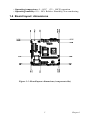
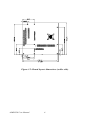
Board layout: dimensions.................................................. 5
2 Installation ........................................................8
2.1
2.2
2.3
2.4
2.5
2.6
2.7
2.8
2.9
2.10
2.11
2.12
2.13
2.14
2.15
2.16
2.17
2.18
2.19
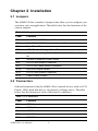
Jumpers.............................................................................. 8
Connectors......................................................................... 8
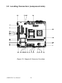
Locating Connectors (component side)........................... 10
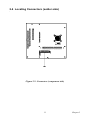
Locating Connectors (solder side)................................... 11
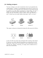
Setting Jumpers ............................................................... 12
USB Controller Power Select (JP2) ................................ 13
USB Wake-up Function (JP3)......................................... 13
Front Panel Connector (JP4) ........................................... 13
COM Ports Ring and Voltage (JP5)................................ 14
COM Ports Ring and COM2 (RS232/422/485)(JP6)...... 14
SM BUS Power Select (JP7)........................................... 15
PCI-X Socket Clock Set (JP8 & JP11)............................ 15
PCI-X Slot Power Select (JP9)........................................ 15
DVO or AGP Alternative Setting (JP10) ........................ 16
Clear CMOS.................................................................... 16
Installing DIMMs............................................................ 16
ATX power control connector (ATX1)........................... 17
Printer port connector (CN3)........................................... 17
CompactFlash Card Socket ............................................. 17
2.19.1 CompactFlash(CN16) ................................................... 17
2.20
Floppy drive connector (CN20) ...................................... 17
2.20.1 Connecting the floppy drive ......................................... 18
2.21
IDE connector(CN17,CN18)........................................... 18
2.21.1 Connecting the hard drive............................................. 18
2.22
VGA/LVDS interface connections.................................. 19
2.22.1 CRT display connector (CN1) ..................................... 19
2.22.2 LVDS LCD panel connector(CN11,VCN1)................. 19
vii