1
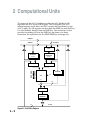
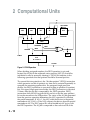
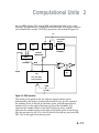
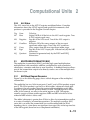
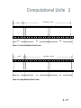
Computational Units
2.1
2
OVERVIEW
This chapter describes the architecture and function of the three
computational units: the arithmetic/logic unit, the multiplier/
accumulator and the barrel shifter.
Every device in the ADSP-2100 family is a 16-bit, fixed-point machine.
Most operations assume a twos-complement number representation,
while others assume unsigned numbers or simple binary strings. Special
features support multiword arithmetic and block floating-point. Details
concerning the various number formats supported by the ADSP-2100
family are given in Appendix C.
In ADSP-2100 family arithmetic, signed numbers are always in twoscomplement format. The processors do not use signed-magnitude, onescomplement, BCD or excess-n formats.
2.1.1
Binary String
This is the simplest binary notation; sixteen bits are treated as a bit pattern.
Examples of computation using this format are the logical operations:
NOT, AND, OR, XOR. These ALU operations treat their operands as
binary strings with no provision for sign bit or binary point placement.
2.1.2
Unsigned
Unsigned binary numbers may be thought of as positive, having nearly
twice the magnitude of a signed number of the same length. The least
significant words of multiple precision numbers are treated as unsigned
numbers.
2.1.3
Signed Numbers: Twos-Complement
In discussions of ADSP-2100 family arithmetic, “signed” refers to twoscomplement. Most ADSP-2100 family operations presume or support
twos-complement arithmetic. The ADSP-2100 family does not use signedmagnitude, ones-complement, BCD or excess-n formats.
2–1
2 Computational Units
2.1.4
Fractional Representation: 1.15
ADSP-2100 family arithmetic is optimized for numerical values in a
fractional binary format denoted by 1.15 (“one dot fifteen”). In the 1.15
format, there is one sign bit (the MSB) and fifteen fractional bits
representing values from –1 up to one LSB less than +1.
Figure 2.1 shows the bit weighting for 1.15 numbers. Below are examples
of 1.15 numbers and their decimal equivalents.
1.15 Number
0x0001
0x7FFF
0xFFFF
0x8000
–2
0
2
–1
2
–2
Decimal Equivalent
0.000031
0.999969
–0.000031
–1.000000
2
–3
2
–4
2
–5
2
–6
2
–7
2
–8
2
–9
2
–10
2
–11
2
–12
2
–13
2
–14
2
–15
Figure 2.1 Bit Weighting For 1.15 Numbers
2.1.5
ALU Arithmetic
All operations on the ALU treat operands and results as simple 16-bit
binary strings, except the signed division primitive (DIVS). Various status
bits treat the results as signed: the overflow (AV) condition code, and the
negative (AN) flag.
The logic of the overflow bit (AV) is based on twos-complement
arithmetic. It is set if the MSB changes in a manner not predicted by the
signs of the operands and the nature of the operation. For example,
adding two positive numbers must generate a positive result; a change in
the sign bit signifies an overflow and sets AV. Adding a negative and a
positive may result in either a negative or positive result, but cannot
overflow.
The logic of the carry bit (AC) is based on unsigned-magnitude arithmetic.
It is set if a carry is generated from bit 16 (the MSB). The (AC) bit is most
useful for the lower word portions of a multiword operation.
2–2
Computational Units 2
2.1.6
MAC Arithmetic
The multiplier produces results that are binary strings. The inputs are
“interpreted” according to the information given in the instruction itself
(signed times signed, unsigned times unsigned, a mixture, or a rounding
operation). The 32-bit result from the multiplier is assumed to be signed,
in that it is sign-extended across the full 40-bit width of the MR register
set.
The ADSP-2100 family supports two modes of format adjustment: the
fractional mode for fractional operands, 1.15 format (1 signed bit, 15
fractional bits), and the integer mode for integer operands, 16.0 format.
When the processor multiplies two 1.15 operands, the result is a 2.30
(2 sign bits, 30 fractional bits) number. In the fractional mode, the MAC
automatically shifts the multiplier product (P) left one bit before
transferring the result to the multiplier result register (MR). This shift
causes the multiplier result to be in 1.31 format, which can be rounded to
1.15 format. Figure 2.7, in the MAC section of this chapter, shows this.
In the integer mode, the left shift does not occur. For example, if the
operands are in the 16.0 format, the 32-bit multiplier result would be in
32.0 format. A left shift is not needed; it would change the numerical
representation. Figure 2.8 in the MAC section of this chapter shows this.
2.1.7
Shifter Arithmetic
Many operations in the shifter are explicitly geared to signed (twoscomplement) or unsigned values: logical shifts assume unsignedmagnitude or binary string values and arithmetic shifts assume twoscomplement.
The exponent logic assumes twos-complement numbers. The exponent
logic supports block floating-point, which is also based on twoscomplement fractions.
2–3
2 Computational Units
2.1.8
Summary
Table 2.1 summarizes some of the arithmetic characteristics of ADSP-2100
family operations. In addition to the numeric types described in this
section, the ADSP-2100 Family C Compiler supports a form of 32-bit
floating-point in which one 16-bit word is the exponent and the other
word is the mantissa. See the ADSP-2100 Family C Tools Manual.
OPERATION
ALU
Operands
Result
Addition
Subtraction
Logical Operations
Division
ALU Overflow
ALU Carry Bit
ALU Saturation
Signed or unsigned
Signed or unsigned
Binary string
Explicitly signed/unsigned
Signed
16-bit unsigned
Signed
Interpret flags
Interpret flags
same as operands
same as operands
same as operands
same as operands
same as operands
1.15 Explicitly signed/unsigned
1.15 Explicitly signed/unsigned
1.15 Explicitly signed/unsigned
1.15 Explicitly signed/unsigned
Signed
32 bits (2.30)
2.30 shifted to 1.31
2.30 shifted to 1.31
2.30 shifted to 1.31
same as operands
1.15 Explicitly signed/unsigned
16.0 Explicitly signed/unsigned
16.0 Explicitly signed/unsigned
16.0 Explicitly signed/unsigned
Signed
32 bits (2.30)
32.0 no shift
32.0 no shift
32.0 no shift
same as operands
Unsigned / binary string
Signed
Signed
same as operands
same as operands
same as operands
ARITHMETIC FORMATS
MAC, Fractional
Multiplication (P)
Multiplication (MR)
Mult / Add
Mult / Subtract
MAC Saturation
MAC, Integer Mode
Multiplication (P)
Multiplication (MR)
Mult / Add
Mult / Subtract
MAC Saturation
Shifter
Logical Shift
Arithmetic Shift
Exponent Detection
Table 2.1 Arithmetic Formats
2–4
Computational Units 2
2.2
ARITHMETIC/LOGIC UNIT (ALU)
The arithmetic/logic unit (ALU) provides a standard set of arithmetic and
logical functions. The arithmetic functions are add, subtract, negate,
increment, decrement and absolute value. These are supplemented by two
division primitives with which multiple cycle division can be constructed.
The logic functions are AND, OR, XOR (exclusive OR) and NOT.
2.2.1
ALU Block Diagram Discussion
Figure 2.2, on the following page, shows a block diagram of the ALU.
The ALU is 16 bits wide with two 16-bit input ports, X and Y, and one
output port, R. The ALU accepts a carry-in signal (CI) which is the carry
bit from the processor arithmetic status register (ASTAT). The ALU
generates six status signals: the zero (AZ) status, the negative (AN) status,
the carry (AC) status, the overflow (AV) status, the X-input sign (AS)
status, and the quotient (AQ) status. All arithmetic status signals are
latched into the arithmetic status register (ASTAT) at the end of the cycle.
Please see the “Instruction Set Reference” chapter of this manual for
information on how each instruction affects the ALU flags.
The X input port of the ALU can accept data from two sources: the AX
register file or the result (R) bus. The R bus connects the output registers of
all the computational units, permitting them to be used as input operands
directly. The AX register file is dedicated to the X input port and consists
of two registers, AX0 and AX1. These AX registers are readable and
writable from the DMD bus. The instruction set also provides for reading
these registers over the PMD bus, but there is no direct connection; this
operation uses the DMD-PMD bus exchange unit. The AX register file
outputs are dual-ported so that one register can provide input to the ALU
while either one simultaneously drives the DMD bus.
The Y input port of the ALU can also accept data from two sources: the
AY register file and the ALU feedback (AF) register. The AY register file is
dedicated to the Y input port and consists of two registers, AY0 and AY1.
These registers are readable and writable from the DMD bus and writable
from the PMD bus. The instruction set also provides for reading these
registers over the PMD bus, but there is no direct connection; this
operation uses the DMD-PMD bus exchange unit. The AY register file
outputs are also dual-ported: one AY register can provide input to the
ALU while either one simultaneously drives the DMD bus.
2–5
2 Computational Units
The output of the ALU is loaded into either the ALU feedback (AF)
register or the ALU result (AR) register. The AF register is an ALU
internal register which allows the ALU result to be used directly as the
ALU Y input. The AR register can drive both the DMD bus and the R bus.
It is also loadable directly from the DMD bus. The instruction set also
provides for reading AR over the PMD bus, but there is no direct
connection; this operation uses the DMD-PMD bus exchange unit.
PMD BUS
24
DMD BUS
16
16 (UPPER)
MUX
AX
REGISTERS
2 x 16
AY
REGISTERS
2 x 16
16
16
MUX
MUX
X
AZ
AN
AC
AV
AS
AQ
Y
ALU
AF
REGISTER
CI
R
16
16
MUX
AR
REGISTER
16
Figure 2.2 ALU Block Diagram
2–6
R - BUS
Computational Units 2
Any of the registers associated with the ALU can be both read and written in
the same cycle. Registers are read at the beginning of the cycle and written at
the end of the cycle. A register read, therefore, reads the value loaded at the
end of a previous cycle. A new value written to a register cannot be read out
until a subsequent cycle. This allows an input register to provide an operand to
the ALU at the beginning of the cycle and be updated with the next operand
from memory at the end of the same cycle. It also allows a result register to be
stored in memory and updated with a new result in the same cycle. See the
discussion of “Multifunction Instructions” in Chapter 15, “Instruction Set
Reference” for an illustration of this same-cycle read and write.
The ALU contains a duplicate bank of registers, shown in Figure 2.2 behind the
primary registers. There are actually two sets of AR, AF, AX, and AY register
files. Only one bank is accessible at a time. The additional bank of registers can
be activated (such as during an interrupt service routine) for extremely fast
context switching. A new task, like an interrupt service routine, can be
executed without transferring current states to storage.
The selection of the primary or alternate bank of registers is controlled by bit 0
in the processor mode status register (MSTAT). If this bit is a 0, the primary
bank is selected; if it is a 1, the secondary bank is selected.
2.2.2
Standard Functions
The standard ALU functions are listed below.
R=X+Y
R = X + Y + CI
R=X–Y
R = X – Y + CI - 1
R=Y–X
R = Y – X + CI - 1
R=–X
R=–Y
R=Y+1
R=Y–1
R = PASS X
R = PASS Y
R = 0 (PASS 0)
R = ABS X
R = X AND Y
R = X OR Y
R = X XOR Y
R = NOT X
R = NOT Y
Add X and Y operands
Add X and Y operands and carry-in bit
Subtract Y from X operand
Subtract Y from X operand with “borrow”
Subtract X from Y operand
Subtract X from Y operand with “borrow”
Negate X operand (twos-complement)
Negate Y operand (twos-complement)
Increment Y operand
Decrement Y operand
Pass X operand to result unchanged
Pass Y operand to result unchanged
Clear result to zero
Absolute value of X operand
Logical AND of X and Y operands
Logical OR of X and Y operands
Logical Exclusive OR of X and Y operands
Logical NOT of X operand (ones-complement)
Logical NOT of Y operand (ones-complement)
2–7
2 Computational Units
2.2.3
ALU Input/Output Registers
The sources of ALU input and output registers are shown below.
Source for
X input port
AX0, AX1
AR
MR0, MR1, MR2
SR0, SR1
Source for
Y input port
AY0, AY1
AF
Destination for
R output port
AR
AF
MR0, MR1 and MR2 are multiplier/accumulator result registers; SR0 and
SR1 are shifter result registers.
2.2.4
Multiprecision Capability
Multiprecision operations are supported in the ALU with the carry-in
signal and ALU carry (AC) status bit. The carry-in signal is the AC status
bit that was generated by a previous ALU operation. The “add with carry”
(+ C) operation is intended for adding the upper portions of
multiprecision numbers. The “subtract with borrow” (C – 1 is effectively a
“borrow”) operation is intended for subtracting the upper portions of
multiprecision numbers.
2.2.5
ALU Saturation Mode
The AR register has a twos-complement saturation mode of operation
which automatically sets it to the maximum negative or positive value if
an ALU result overflows or underflows. This feature is enabled by setting
bit 3 of the mode status register (MSTAT). When enabled, the value loaded
into AR during an ALU operation depends on the state of the overflow
and carry status generated by the ALU on that cycle. The following table
summarizes the loading of AR when saturation mode is enabled.
Overflow (AV)
0
0
1
1
Carry (AC)
0
1
0
1
AR Contents
ALU Output
ALU Output
0111111111111111
1000000000000000
full-scale positive
full-scale negative
Table 2.2 Saturation Mode
The operation of the ALU saturation mode is different from the
Multiplier/Accumulator saturation ability, which is enabled only on an
instruction by instruction basis. For the ALU, enabling saturation means
that all subsequent operations are processed this way.
2–8
Computational Units 2
When the ALU saturation mode is used, only the AR register saturates; if
the AF register is the destination, wrap-around will occur but the flags
will reflect the saturated result.
2.2.6
ALU Overflow Latch Mode
The ALU overflow latch mode, enabled by setting bit 2 in the mode status
register (MSTAT), causes the AV bit to “stick” once it is set. In this mode,
when an ALU overflow occurs, AV will be set and remain set, even if
subsequent ALU operations do not generate overflows. In this mode, AV
can only be cleared by writing a zero to it directly from the DMD bus.
2.2.7
Division
The ALU supports division. The divide function is achieved with
additional shift circuitry not shown in Figure 2.2. Division is accomplished
with two special divide primitives. These are used to implement a nonrestoring conditional add-subtract division algorithm. The division can be
either signed or unsigned; however, the dividend and divisor must both
be of the same type. Appendix B details various exceptions to the normal
division operation as described in this section.
A single-precision divide, with a 32-bit dividend (numerator) and a 16-bit
divisor (denominator), yielding a 16-bit quotient, executes in 16 cycles.
Higher and lower precision quotients can also be calculated. The divisor
can be stored in AX0, AX1 or any of the R registers. The upper half of a
signed dividend can start in either AY1 or AF. The upper half of an
unsigned dividend must be in AF. The lower half of any dividend must be
in AY0. At the end of the divide operation, the quotient will be in AY0.
The first of the two primitive instructions “divide-sign” (DIVS) is executed
at the beginning of the division when dividing signed numbers. This
operation computes the sign bit of the quotient by performing an
exclusive-OR of the sign bits of the divisor and the dividend. The AY0
register is shifted one place so that the computed sign bit is moved into
the LSB position. The computed sign bit is also loaded into the AQ bit of
the arithmetic status register. The MSB of AY0 shifts into the LSB position
of AF, and the upper 15 bits of AF are loaded with the lower 15 R bits
from the ALU, which simply passes the Y input value straight through to
the R output. The net effect is to left shift the AF-AY0 register pair and
move the quotient sign bit into the LSB position. The operation of DIVS is
illustrated in Figure 2.3 (on the next page).
2–9
2 Computational Units
15
LEFT SHIFT
AX0
AX1
AY1
AF
L
S
B
LOWER
DIVIDEND
16
MUX
AY0
MUX
UPPER
DIVIDEND
MSB
MSB
DIVISOR
R-BUS
AQ
X
Y
ALU
R = PASS Y
15 LSBs
Figure 2.3 DIVS Operation
When dividing unsigned numbers, the DIVS operation is not used.
Instead, the AQ bit in the arithmetic status register (ASTAT) should be
initialized to zero by manually clearing it. The AQ bit indicates to the
following operations that the quotient should be assumed positive.
The second division primitive is the “divide-quotient” (DIVQ) instruction
which generates one bit of quotient at a time and is executed repeatedly to
compute the remaining quotient bits. For unsigned single precision
divides, the DIVQ instruction is executed 16 times to produce 16 quotient
bits. For signed single precision divides, the DIVQ instruction is executed
15 times after the sign bit is computed by the DIVS operation. DIVQ
instruction shifts the AY0 register left by one bit so that the new quotient
bit can be moved into the LSB position. The status of the AQ bit generated
from the previous operation determines the ALU operation to calculate
the partial remainder. If AQ = 1, the ALU adds the divisor to the partial
remainder in AF. If AQ = 0, the ALU subtracts the divisor from the partial
remainder in AF. The ALU output R is offset loaded into AF just as with
the DIVS operation. The AQ bit is computed as the exclusive-OR of the
2 – 10
Computational Units 2
divisor MSB and the ALU output MSB, and the quotient bit is this value
inverted. The quotient bit is loaded into the LSB of the AY0 register which is
also shifted left by one bit. The DIVQ operation is illustrated in Figure 2.4.
15
LEFT SHIFT
AF
AX1
AX0
L
S
B
AY0
LOWER
DIVIDEND
PARTIAL
REMAINDER
MUX
16
DIVISOR
R-BUS
MSB
X
AQ
Y
ALU
R=Y+X IF AQ=1
R=Y-X IF AQ=0
1 MSB
15 LSBs
Figure 2.4 DIVQ Operation
The format of the quotient for any numeric representation can be
determined by the format of the dividend and divisor. Let NL represent
the number of bits to the left of the binary point, and NR represent the
number of bits to the right of the binary point of the dividend; DL
represent the number of bits to the left of the binary point, and DR
represent the number of bits to the right of the binary point of the divisor;
then the quotient has NL–DL+1 bits to the left of the binary point and NR–
DR–1 bits to the right of the binary point.
2 – 11
2 Computational Units
Some format manipulation may be necessary to guarantee the validity of
the quotient. For example, if both operands are signed and fully fractional
(dividend in 1.31 format and divisor in 1.15 format) the result is fully
fractional (in 1.15 format) and therefore the dividend must be smaller than
the divisor for a valid result.
To divide two integers (dividend in 32.0 format and divisor in 16.0 format)
and produce an integer quotient (in 16.0 format), you must shift the
dividend one bit to the left (into 31.1 format) before dividing. Additional
discussion and code examples can be found in the handbook Digital Signal
Processing Applications Using the ADSP-2100 Family, Volume 1.
Dividend
BBBBB.BBBBBBBBBBBBBBBBBBBBBBBBBBB
NL bits
Divisor
BB.BBBBBBBBBBBBBB
DL bits
Quotient
NR bits
DR bits
BBBB.BBBBBBBBBBBB
(NL–DL+1) bits
(NR–DR–1) bits
Figure 2.5 Quotient Format
The algorithm overflows if the result cannot be represented in the format
of the quotient as calculated above or when the divisor is zero or less than
the dividend in magnitude.
2 – 12
Computational Units 2
2.2.8
ALU Status
The ALU status bits in the ASTAT register are defined below. Complete
information about the ASTAT register and specific bit mnemonics and
positions is provided in the Program Control chapter.
Flag
AZ
Name
Zero
AN
Negative
AV
Overflow
AC
AS
Carry
Sign
AQ
Quotient
2.3
Definition
Logical NOR of all the bits in the ALU result register. True
if ALU output equals zero.
Sign bit of the ALU result. True if the ALU output is
negative.
Exclusive-OR of the carry outputs of the two most
significant adder stages. True if the ALU overflows.
Carry output from the most significant adder stage.
Sign bit of the ALU X input port. Affected only by the ABS
instruction.
Quotient bit generated only by the DIVS and DIVQ
instructions.
MULTIPLIER/ACCUMULATOR (MAC)
The multiplier/accumulator (MAC) provides high-speed multiplication,
multiplication with cumulative addition, multiplication with cumulative
subtraction, saturation and clear-to-zero functions. A feedback function allows
part of the accumulator output to be directly used as one of the multiplicands
on the next cycle.
2.3.1
MAC Block Diagram Discussion
Figure 2.6, on the following page, shows a block diagram of the multiplier/
accumulator.
The multiplier has two 16-bit input ports X and Y, and a 32-bit product output
port P. The 32-bit product is passed to a 40-bit adder/subtracter which adds
or subtracts the new product from the content of the multiplier result (MR)
register, or passes the new product directly to MR. The MR register is 40 bits
wide. In this manual, we refer to the entire register as MR. The register
actually consists of three smaller registers: MR0 and MR1 which are 16 bits
wide and MR2 which is 8 bits wide.
The adder/subtracter is greater than 32 bits to allow for intermediate overflow
in a series of multiply/accumulate operations. The multiply overflow (MV)
status bit is set when the accumulator has overflowed beyond the 32-bit
boundary, that is, when there are significant (non-sign) bits in the top nine bits
of the MR register (based on twos-complement arithmetic).
2 – 13
2 Computational Units
PMD BUS
24
DMD BUS
16
16 (UPPER)
MUX
MX
REGISTERS
2 x 16
MY
REGISTERS
2 x 16
16
16
MUX
MUX
X
Y
MF
REGISTER
MULTIPLIER
P
40
32
16
ADD / SUBTRACT
R2
MV
R1
MUX
R0
MUX
8
MUX
16
MR2
REGISTER
16
MR1
REGISTER
MR0
REGISTER
M
U
X
16
Figure 2.6 MAC Block Diagram
2 – 14
R - BUS
Computational Units 2
The input/output registers of the MAC are similar to the ALU.
The X input port can accept data from either the MX register file or from
any register on the result (R) bus. The R bus connects the output registers
of all the computational units, permitting them to be used as input
operands directly. There are two registers in the MX register file, MX0 and
MX1. These registers can be read and written from the DMD bus. The MX
register file outputs are dual-ported so that one register can provide input
to the multiplier while either one simultaneously drives the DMD bus.
The Y input port can accept data from either the MY register file or the MF
register. The MY register file has two registers, MY0 and MY1; these
registers can be read and written from the DMD bus and written from the
PMD bus. The instruction set also provides for reading these registers over
the PMD bus, but there is no direct connection; this operation uses the
DMD-PMD bus exchange unit. The MY register file outputs are also dualported so that one register can provide input to the multiplier while either
one simultaneously drives the DMD bus.
The output of the adder/subtracter goes to either the MF register or the
MR register. The MF register is a feedback register which allows bits 16–31
of the result to be used directly as the multiplier Y input on a subsequent
cycle. The 40-bit adder/subtracter register (MR) is divided into three
sections: MR2, MR1, and MR0. Each of these registers can be loaded
directly from the DMD bus and output to either the DMD bus or the R
bus.
Any of the registers associated with the MAC can be both read and
written in the same cycle. Registers are read at the beginning of the cycle
and written at the end of the cycle. A register read, therefore, reads the
value loaded at the end of a previous cycle. A new value written to a
register cannot be read out until a subsequent cycle. This allows an input
register to provide an operand to the MAC at the beginning of the cycle
and be updated with the next operand from memory at the end of the
same cycle. It also allows a result register to be stored in memory and
updated with a new result in the same cycle. See the discussion of
“Multifunction Instructions” in Chapter 15 “Instruction Set Reference” for
an illustration of this same-cycle read and write.
2 – 15
2 Computational Units
The MAC contains a duplicate bank of registers, shown in Figure 2.6
behind the primary registers. There are actually two sets of MR, MF, MX,
and MY register files. Only one bank is accessible at a time. The additional
bank of registers can be activated for extremely fast context switching. A
new task, such as an interrupt service routine, can be executed without
transferring current states to storage.
The selection of the primary or alternate bank of registers is controlled by
bit 0 in the processor mode status register (MSTAT). If this bit is a 0, the
primary bank is selected; if it is a 1, the secondary bank is selected.
2.3.2
MAC Operations
This section explains the functions of the MAC, its input formats and its
handling of overflow and saturation.
2.3.2.1 Standard Functions
The functions performed by the MAC are:
X*Y
MR+X*Y
MR–X*Y
0
Multiply X and Y operands.
Multiply X and Y operands and add result to MR register.
Multiply X and Y operands and subtract result from MR register.
Clear result (MR) to zero.
The ADSP-2100 family provides two modes for the standard multiply/
accumulate function: fractional mode for fractional numbers (1.15), and
integer mode for integers (16.0).
In the fractional mode, the 32-bit P output is format adjusted, that is, signextended and shifted one bit to the left before being added to MR. For
example, bit 31 of P lines up with bit 32 of MR (which is bit 0 of MR2) and
bit 0 of P lines up with bit 1 of MR (which is bit 1 of MR0). The LSB is zerofilled. The fractional multiplier result format is shown in Figure 2.7.
In the integer mode, the 32-bit P register is not shifted before being added
to MR. Figure 2.8 shows the integer-mode result placement.
The mode is selected by bit 4 of the mode status register (MSTAT). If this
bit is a 1, the integer mode is selected. Otherwise, the fractional mode is
selected. In either mode, the multiplier output P is fed into a 40-bit adder/
subtracter which adds or subtracts the new product with the current
contents of the MR register to form the final 40-bit result R.
2 – 16
Computational Units 2
MULTIPLIER P OUTPUT
P SIGN
31 31 31 31 31 31 31 31 30 29 28 27 26 25 24 23 22 21 20 19 18 17 16 15 14 13 12 11 10 9
7
6
5
4
3
2
1
0
15 14 13 12 11 10 9
8
MR2
7
6
5
4
3
2
1
0
8
7
6
5
4
3
2
1
0
15 14 13 12 11 10 9
8
7
6
5
4
3
2
1
0
MR1
MR0
Figure 2.7 Fractional Multiplier Result Format
P SIGN
MULTIPLIER P OUTPUT
31 31 31 31 31 31 31 31 31 30 29 28 27 26 25 24 23 22 21 20 19 18 17 16 15 14 13 12 11 10 9
8
7
6
5
4
3
2
1
0
7
8
7
6
5
4
3
2
1
0
6
5
4
3
MR2
2
1
0
15 14 13 12 11 10 9
8
7
6
MR1
5
4
3
2
1
0
15 14 13 12 11 10 9
MR0
Figure 2.8 Integer Multiplier Result Format
2 – 17
2 Computational Units
2.3.2.2 Input Formats
To facilitate multiprecision multiplications, the multiplier accepts X and Y
inputs represented in any combination of signed twos-complement format
and unsigned format.
X input
signed
unsigned
signed
unsigned
x
x
x
x
Y input
signed
signed
unsigned
unsigned
The input formats are specified as part of the instruction. These are
dynamically selectable each time the multiplier is used.
The (signed x signed) mode is used when multiplying two signed single
precision numbers or the two upper portions of two signed multiprecision
numbers.
The (unsigned x signed) and (signed x unsigned) modes are used when
multiplying the upper portion of a signed multiprecision number with the
lower portion of another or when multiplying a signed single precision
number by an unsigned single precision number.
The (unsigned x unsigned) mode is used when multiplying unsigned
single precision numbers or the non-upper portions of two signed
multiprecision numbers.
2.3.2.3 MAC Input/Output Registers
The sources of MAC input and output are:
Source for
X input port
MX0, MX1
AR
MR0, MR1, MR2
SR0, SR1
Source for
Y input port
MY0, MY1
MF
Destination for
R output port
MR (MR2, MR1, MR0)
MF
2.3.2.4 MR Register Operation
As described, and shown on the block diagram, the MR register is divided
into three sections: MR0 (bits 0-15), MR1 (bits 16-31), and MR2 (bits 3239). Each of these registers can be loaded from the DMD bus and output to
the R bus or the DMD bus.
2 – 18
Computational Units 2
The 8-bit MR2 register is tied to the lower 8 bits of these buses. When MR2
is output onto the DMD bus or the R bus, it is sign extended to form a 16bit value. MR1 also has an automatic sign-extend capability. When MR1 is
loaded from the DMD bus, every bit in MR2 will be set to the sign bit
(MSB) of MR1, so that MR2 appears as an extension of MR1. To load the
MR2 register with a value other than MR1’s sign extension, you must load
MR2 after MR1 has been loaded. Loading MR0 affects neither MR1 nor
MR2; no sign extension occurs in MR0 loads.
2.3.2.5 MAC Overflow And Saturation
The adder/subtracter generates an overflow status signal (MV) which is
loaded into the processor arithmetic status (ASTAT) every time a MAC
operation is executed. The MV bit is set when the accumulator result,
interpreted as a twos-complement number, crosses the 32-bit (MR1/MR2)
boundary. That is, MV is set if the upper nine bits of MR are not all ones or
all zeros.
The MR register has a saturation capability which sets MR to the
maximum positive or negative value if an overflow or underflow has
occurred. The saturation operation depends on the overflow status bit
(MV) in the processor arithmetic status (ASTAT) and the MSB of the MR2
register. The following table summarizes the MR saturation operation.
MV
0
1
1
MSB of MR2
0 or 1
0
1
MR contents after saturation
no change
00000000 0111111111111111 1111111111111111
11111111 1000000000000000 0000000000000000
full-scale positive
full-scale negative
Table 2.3 Effect Of MAC Saturation Instruction
Saturation in the MAC is an instruction rather than a mode as in the ALU.
The saturation instruction is intended to be used at the completion of a
string of multiplication/accumulations so that intermediate overflows do
not cause the accumulator to saturate.
Overflowing beyond the MSB of MR2 should never be allowed. The true
sign bit of the result is then irretrievably lost and saturation may not
produce a correct value. It takes more than 255 overflows (MV type) to
reach this state, however.
2 – 19
2 Computational Units
2.3.2.6 Rounding Mode
The accumulator has the capability for rounding the 40-bit result R at the
boundary between bit 15 and bit 16. Rounding can be specified as part of
the instruction code. The rounded output is directed to either MR or MF.
When rounding is invoked with MF as the output register, register
contents in MF represent the rounded 16-bit result. Similarly, when MR is
selected as the output, MR1 contains the rounded 16-bit result; the
rounding effect in MR1 affects MR2 as well and MR2 and MR1 represent
the rounded 24-bit result.
The accumulator uses an unbiased rounding scheme. The conventional
method of biased rounding is to add a 1 into bit position 15 of the adder
chain. This method causes a net positive bias since the midway value
(when MR0=0x8000) is always rounded upward. The accumulator
eliminates this bias by forcing bit 16 in the result output to zero when it
detects this midway point. This has the effect of rounding odd MR1 values
upward and even MR1 values downward, yielding a zero large-sample
bias assuming uniformly distributed values.
Using x to represent any bit pattern (not all zeros), here are two examples
of rounding. The first example is the typical rounding operation.
Example 1
MR2
MR1
Unrounded value:
xxxxxxxx
xxxxxxxx00100101 1xxxxxxxxxxxxxxx
Bit 15 = 1
Add 1 to bit 15 and carry
Rounded value:
xxxxxxxx
MR0
1
xxxxxxxx00100110 0xxxxxxxxxxxxxxx
The compensation to avoid net bias becomes visible when the lower 15
bits are all zero and bit 15 is one, i.e. the midpoint value.
2 – 20
Computational Units 2
Example 2
MR2
MR1
Unrounded value:
xxxxxxxx
xxxxxxxx01100110 1000000000000000
Bit 15 = 1 and bits 0-14 = 0
Add 1 to bit 15 and carry
MR0
1
xxxxxxxx
xxxxxxxx01100111 0000000000000000
Since bit 16 = 1, force it to 0
Rounded value:
xxxxxxxx
xxxxxxxx01100110 0000000000000000
In this last case, bit 16 is forced to zero. This algorithm is employed on every
rounding operation, but is only evident when the bit patterns shown in the
lower 16 bits of the last example are present.
2.3.2.7 Biased Rounding (ADSP-217x, ADSP-218x, ADSP-21msp5x)
A mode is available on the ADSP-217x, ADSP-218x, and ADSP-21msp58/
59 processors to allow biased rounding in addition to the normal unbiased
rounding. This mode is selected by the BIASRND bit (bit 12 of the SPORT0
Autobuffer Control register). When the BIASRND bit is set to 0, the normal
unbiased rounding operations occur. When the BIASRND bit is set to 1,
biased rounding occurs instead of the normal unbiased rounding. When
operating in biased rounding mode all rounding operations with MR0 set
to 0x8000 will round up, rather than only rounding odd MR1 values up.
For example:
MR value before RND
00-0000-8000
00-0001-8000
00-0000-8001
00-0001-8001
00-0000-7FFF
00-0001-7FFF
biased RND result
00-0001-8000
00-0002-8000
00-0001-8001
00-0002-8001
00-0000-7FFF
00-0001-7FFF
unbiased RND result
00-0000-8000
00-0002-8000
00-0001-8001
00-0002-8001
00-0000-7FFF
00-0001-7FFF
This mode only has an effect when the MR0 register contains 0x8000; all
other rounding operations work normally. This mode allows more efficient
implementation of bit-specified algorithms that use biased rounding, for
example the GSM speech compression routines. Unbiased rounding is
preferred for most algorithms.
2 – 21
2 Computational Units
2.4
BARREL SHIFTER
The shifter provides a complete set of shifting functions for 16-bit inputs,
yielding a 32-bit output. These include arithmetic shift, logical shift and
normalization. The shifter also performs derivation of exponent and
derivation of common exponent for an entire block of numbers. These
basic functions can be combined to efficiently implement any degree of
numerical format control, including full floating-point representation.
2.4.1
Shifter Block Diagram Discussion
Figure 2.9 shows a block diagram of the shifter. The shifter can be divided
into the following components: the shifter array, the OR/PASS logic, the
exponent detector, and the exponent compare logic.
The shifter array is a 16x32 barrel shifter. It accepts a 16-bit input and can
place it anywhere in the 32-bit output field, from off-scale right to off-scale
left, in a single cycle. This gives 49 possible placements within the 32-bit
field. The placement of the 16 input bits is determined by a control code
(C) and a HI/LO reference signal.
The shifter array and its associated logic are surrounded by a set of
registers. The shifter input (SI) register provides input to the shifter array
and the exponent detector. The SI register is 16 bits wide and is readable
and writable from the DMD bus. The shifter array and the exponent
detector also take as inputs AR, SR or MR via the R bus. The shifter result
(SR) register is 32 bits wide and is divided into two 16-bit sections, SR0
and SR1. The SR0 and SR1 registers can be loaded from the DMD bus and
output to either the DMD bus or the R bus. The SR register is also fed back
to the OR/PASS logic to allow double-precision shift operations.
The SE register (“shifter exponent”) is 8 bits wide and holds the exponent
during the normalize and denormalize operations. The SE register is
loadable and readable from the lower 8 bits of the DMD bus. It is a twoscomplement, 8.0 value.
The SB register (“shifter block”) is important in block floating-point
operations where it holds the block exponent value, that is, the value by
which the block values must be shifted to normalize the largest value. SB
is 5 bits wide and holds the most recent block exponent value. The SB
register is loadable and readable from the lower 5 bits of the DMD bus. It
is a twos-complement, 5.0 value.
Whenever the SE or SB registers are output onto the DMD bus, they are
sign-extended to form a 16-bit value.
2 – 22
Computational Units 2
DMD BUS
16
SI
REGISTER
MUX
SB
REGISTER
MUX
SS
8
MUX
X
EXPONENT
DETECTOR
COMPARE
HI / LO
R
C
I
X
SHIFTER
ARRAY
O
32
MUX
32
OR / PASS
SE
REGISTER
NEGATE
8
From
INSTRUCTION
16
16
MUX
MUX
SR1
REGISTER
SR0
REGISTER
16
R - BUS
16
MUX
16
Figure 2.9 Shifter Block Diagram
Any of the SI, SE or SR registers can be read and written in the same cycle.
Registers are read at the beginning of the cycle and written at the end of
the cycle. All register reads, therefore, read values loaded at the end of a
previous cycle. A new value written to a register cannot be read out until a
subsequent cycle. This allows an input register to provide an operand to
the shifter at the beginning of the cycle and be updated with the next
operand at the end of the same cycle. It also allows a result register to be
stored in memory and updated with a new result in the same cycle. See
the discussion of “Multifunction Instructions” in Chapter 15, “Instruction
Set Reference” for an illustration of this same-cycle read and write.
2 – 23
2 Computational Units
The shifter contains a duplicate bank of registers, shown in Figure 2.9
behind the primary registers. There are actually two sets of SE, SB, SI, SR1,
and SR0 registers. Only one bank is accessible at a time. The additional
bank of registers can be activated for extremely fast context switching. A
new task, such as an interrupt service routine, can then be executed
without transferring current states to storage.
The selection of the primary or alternate bank of registers is controlled by
bit 0 in the processor mode status register (MSTAT). If this bit is a 0, the
primary bank is selected; if it is a 1, the secondary bank is selected.
The shifting of the input is determined by a control code (C) and a HI/LO
reference signal. The control code is an 8-bit signed value which indicates
the direction and number of places the input is to be shifted. Positive
codes indicate a left shift (upshift) and negative codes indicate a right shift
(downshift). The control code can come from three sources: the content of
the shifter exponent (SE) register, the negated content of the SE register or
an immediate value from the instruction.
The HI/LO signal determines the reference point for the shifting. In the HI
state, all shifts are referenced to SR1 (the upper half of the output field),
and in the LO state, all shifts are referenced to SR0 (the lower half). The
HI/LO reference feature is useful when shifting 32-bit values since it
allows both halves of the number to be shifted with the same control code.
HI/LO reference signal is selectable each time the shifter is used.
The shifter fills any bits to the right of the input value in the output field
with zeros, and bits to the left are filled with the extension bit (X). The
extension bit can be fed by three possible sources depending on the
instruction being performed. The three sources are the MSB of the input,
the AC bit from the arithmetic status register (ASTAT) or a zero.
Table 2.4 shows the shifter array output as a function of the control code
and HI/LO signal.
The OR/PASS logic allows the shifted sections of a multiprecision number
to be combined into a single quantity. In some shifter instructions, the
shifted output may be logically ORed with the contents of the SR register;
the shifter array is bitwise ORed with the current contents of the SR
register before being loaded there. When the [SR OR] option is not used in
the instruction, the shifter array output is passed through and loaded into
the shifter result (SR) register unmodified.
2 – 24
Computational Units 2
Control Code
HI reference
LO Reference
+16 to +127
+15
+14
+13
+12
+11
+10
+9
+8
+7
+6
+5
+4
+3
+2
+1
0
-1
-2
-3
-4
-5
-6
-7
-8
-9
-10
-11
-12
-13
-14
-15
-16
-17
-18
-19
-20
-21
-22
-23
-24
-25
-26
-27
-28
-29
-30
-31
-32 to -128
+32 to +127
+31
+30
+29
+28
+27
+26
+25
+24
+23
+22
+21
+20
+19
+18
+17
+16
+15
+14
+13
+12
+11
+10
+9
+8
+7
+6
+5
+4
+3
+2
+1
0
-1
-2
-3
-4
-5
-6
-7
-8
-9
-10
-11
-12
-13
-14
-15
-16 to -128
Shifter Array Output
00000000
R0000000
PR000000
NPR00000
MNPR0000
LMNPR000
KLMNPR00
JKLMNPR0
IJKLMNPR
HIJKLMNP
GHIJKLMN
FGHIJKLM
EFGHIJKL
DEFGHIJK
CDEFGHIJ
BCDEFGHI
ABCDEFGH
XABCDEFG
XXABCDEF
XXXABCDE
XXXXABCD
XXXXXABC
XXXXXXAB
XXXXXXXA
XXXXXXXX
XXXXXXXX
XXXXXXXX
XXXXXXXX
XXXXXXXX
XXXXXXXX
XXXXXXXX
XXXXXXXX
XXXXXXXX
XXXXXXXX
XXXXXXXX
XXXXXXXX
XXXXXXXX
XXXXXXXX
XXXXXXXX
XXXXXXXX
XXXXXXXX
XXXXXXXX
XXXXXXXX
XXXXXXXX
XXXXXXXX
XXXXXXXX
XXXXXXXX
XXXXXXXX
XXXXXXXX
00000000
00000000
00000000
00000000
00000000
00000000
00000000
00000000
00000000
R0000000
PR000000
NPR00000
MNPR0000
LMNPR000
KLMNPR00
JKLMNPR0
IJKLMNPR
HIJKLMNP
GHIJKLMN
FGHIJKLM
EFGHIJKL
DEFGHIJK
CDEFGHIJ
BCDEFGHI
ABCDEFGH
XABCDEFG
XXABCDEF
XXXABCDE
XXXXABCD
XXXXXABC
XXXXXXAB
XXXXXXXA
XXXXXXXX
XXXXXXXX
XXXXXXXX
XXXXXXXX
XXXXXXXX
XXXXXXXX
XXXXXXXX
XXXXXXXX
XXXXXXXX
XXXXXXXX
XXXXXXXX
XXXXXXXX
XXXXXXXX
XXXXXXXX
XXXXXXXX
XXXXXXXX
XXXXXXXX
ABCDEFGHIJKLMNPR
represents the 16-bit
input pattern
00000000
00000000
00000000
00000000
00000000
00000000
00000000
00000000
00000000
00000000
00000000
00000000
00000000
00000000
00000000
00000000
00000000
R0000000
PR000000
NPR00000
MNPR0000
LMNPR000
KLMNPR00
JKLMNPR0
IJKLMNPR
HIJKLMNP
GHIJKLMN
FGHIJKLM
EFGHIJKL
DEFGHIJK
CDEFGHIJ
BCDEFGHI
ABCDEFGH
XABCDEFG
XXABCDEF
XXXABCDE
XXXXABCD
XXXXXABC
XXXXXXAB
XXXXXXXA
XXXXXXXX
XXXXXXXX
XXXXXXXX
XXXXXXXX
XXXXXXXX
XXXXXXXX
XXXXXXXX
XXXXXXXX
XXXXXXXX
00000000
00000000 X stands for the
00000000 extension bit
00000000
00000000
00000000
00000000
00000000
00000000
00000000
00000000
00000000
00000000
00000000
00000000
00000000
00000000
00000000
00000000
00000000
00000000
00000000
00000000
00000000
00000000
R0000000
PR000000
NPR00000
MNPR0000
LMNPR000
KLMNPR00
JKLMNPR0
IJKLMNPR
HIJKLMNP
GHIJKLMN
FGHIJKLM
EFGHIJKL
DEFGHIJK
CDEFGHIJ
BCDEFGHI
ABCDEFGH
XABCDEFG
XXABCDEF
XXXABCDE
XXXXABCD
XXXXXABC
XXXXXXAB
XXXXXXXA
XXXXXXXX
Table 2.4 Shifter Array Characteristic
2 – 25
2 Computational Units
The exponent detector derives an exponent for the shifter input value. The
exponent detector operates in one of three ways which determine how the
input value is interpreted. In the HI state, the input is interpreted as a
single precision number or the upper half of a double precision number.
The exponent detector determines the number of leading sign bits and
produces a code which indicates how many places the input must be upshifted to eliminate all but one of the sign bits. The code is negative so that
it can become the effective exponent for the mantissa formed by removing
the redundant sign bits.
In the HI-extend state (HIX), the input is interpreted as the result of an
add or subtract performed in the ALU which may have overflowed.
Therefore the exponent detector takes the arithmetic overflow (AV) status
into consideration. If AV is set, then a +1 exponent is output to indicate an
extra bit is needed in the normalized mantissa (the ALU Carry bit); if AV
is not set, then HI-extend functions exactly like the HI state. When
performing a derive exponent function in HI or HI-extend modes, the
exponent detector also outputs a shifter sign (SS) bit which is loaded into
the arithmetic status register (ASTAT). The sign bit is the same as the MSB
of the shifter input except when AV is set; when AV is set in HI-extend
state, the MSB is inverted to restore the sign bit of the overflowed value.
In the LO state, the input is interpreted as the lower half of a double
precision number. In the LO state, the exponent detector interprets the SS
bit in the arithmetic status register (ASTAT) as the sign bit of the number.
The SE register is loaded with the output of the exponent detector only if
SE contains –15. This occurs only when the upper half–which must be
processed first–contained all sign bits. The exponent detector output is
also offset by –16 to account for the fact that the input is actually the lower
half of a 32-bit value. Table 2.5 gives the exponent detector characteristics
for all three modes.
The exponent compare logic is used to find the largest exponent value in
an array of shifter input values. The exponent compare logic in
conjunction with the exponent detector derives a block exponent. The
comparator compares the exponent value derived by the exponent
detector with the value stored in the shifter block exponent (SB) register
and updates the SB register only when the derived exponent value is
larger than the value in SB register. See the examples shown in the
following sections.
2 – 26
Computational Units 2
S = Sign bit
N = Non-sign bit
D = Don’t care bit
HI Mode
HIX Mode
Shifter Array Input
Output
AV
Shifter Array Input
Output
SNDDDDDD
SSNDDDDD
SSSNDDDD
SSSSNDDD
SSSSSNDD
SSSSSSND
SSSSSSSN
SSSSSSSS
SSSSSSSS
SSSSSSSS
SSSSSSSS
SSSSSSSS
SSSSSSSS
SSSSSSSS
SSSSSSSS
SSSSSSSS
0
-1
-2
-3
-4
-5
-6
-7
-8
-9
-10
-11
-12
-13
-14
-15
1
0
0
0
0
0
0
0
0
0
0
0
0
0
0
0
0
DDDDDDDD
SNDDDDDD
SSNDDDDD
SSSNDDDD
SSSSNDDD
SSSSSNDD
SSSSSSND
SSSSSSSN
SSSSSSSS
SSSSSSSS
SSSSSSSS
SSSSSSSS
SSSSSSSS
SSSSSSSS
SSSSSSSS
SSSSSSSS
SSSSSSSS
+1
0
-1
-2
-3
-4
-5
-6
-7
-8
-9
-10
-11
-12
-13
-14
-15
DDDDDDDD
DDDDDDDD
DDDDDDDD
DDDDDDDD
DDDDDDDD
DDDDDDDD
DDDDDDDD
NDDDDDDD
SNDDDDDD
SSNDDDDD
SSSNDDDD
SSSSNDDD
SSSSSNDD
SSSSSSND
SSSSSSSN
SSSSSSSS
DDDDDDDD
DDDDDDDD
DDDDDDDD
DDDDDDDD
DDDDDDDD
DDDDDDDD
DDDDDDDD
DDDDDDDD
NDDDDDDD
SNDDDDDD
SSNDDDDD
SSSNDDDD
SSSSNDDD
SSSSSNDD
SSSSSSND
SSSSSSSN
SSSSSSSS
LO Mode
SS
Shifter Array Input
Output
S
S
S
S
S
S
S
S
S
S
S
S
S
S
S
S
S
NDDDDDDD
SNDDDDDD
SSNDDDDD
SSSNDDDD
SSSSNDDD
SSSSSNDD
SSSSSSND
SSSSSSSN
SSSSSSSS
SSSSSSSS
SSSSSSSS
SSSSSSSS
SSSSSSSS
SSSSSSSS
SSSSSSSS
SSSSSSSS
SSSSSSSS
-15
-16
-17
-18
-19
-20
-21
-22
-23
-24
-25
-26
-27
-28
-29
-30
-31
DDDDDDDD
DDDDDDDD
DDDDDDDD
DDDDDDDD
DDDDDDDD
DDDDDDDD
DDDDDDDD
DDDDDDDD
NDDDDDDD
SNDDDDDD
SSNDDDDD
SSSNDDDD
SSSSNDDD
SSSSSNDD
SSSSSSND
SSSSSSSN
SSSSSSSS
Table 2.5 Exponent Detector Characteristics
2 – 27
2 Computational Units
2.4.2
Shifter Operations
The shifter performs the following functions (instruction mnemonics
shown in parentheses):
•
•
•
•
•
Arithmetic Shift (ASHIFT)
Logical Shift (LSHIFT)
Normalize (NORM)
Derive Exponent (EXP)
Block Exponent Adjust (EXPADJ)
These basic shifter instructions can be used in a variety of ways,
depending on the underlying arithmetic requirements. The following
sections present single and multiple precision examples for these
functions:
•
•
•
•
Derivation of a Block Exponent
Immediate Shifts
Denormalization
Normalization
The shift functions (arithmetic shift, logical shift, and normalize) can be
optionally specified with [SR OR] and HI/LO modes to facilitate
multiprecision operations. [SR OR] logically ORs the shift result with the
current contents of SR. This option is used to join two 16-bit quantities into
a 32-bit value in SR. When [SR OR] is not used, the shift value is passed
through to SR directly. The HI and LO modifiers reference the shift to the
upper or lower half of the 32-bit SR register. These shift functions take
inputs from either the SI register or any other result register and load the
32-bit shifted result into the SR register.
2.4.2.1 Shifter Input/Output Registers
The sources of shifter input and output are:
Source for
Shifter input
SI
AR
MR0, MR1, MR2
SR0, SR1
2 – 28
Destination for
Shifter output
SR (SR0, SR1)
Computational Units 2
2.4.2.2 Derive Block Exponent
This function detects the exponent of the number largest in magnitude in
an array of numbers. The EXPADJ instruction performs this function. The
sequence of steps for a typical example is shown below.
A. Load SB with –16
The SB register is used to contain the exponent for the entire block. The
possible values at the conclusion of a series of EXPADJ operations range
from –15 to 0. The exponent compare logic updates the SB register if the
new value is greater than the current value. Loading the register with –16
initializes it to a value certain to be less than any actual exponents
detected.
B. Process the first array element:
Array(1) =
11110101 10110001
Exponent = –3
– 3 > SB (–16)
SB gets
–3
C. Process next array element:
Array(2)=
00000001 01110110
Exponent = –6
–6 < –3
SB remains
–3
D. Continue processing array elements.
When and if an array element is found whose exponent is greater than SB,
that value is loaded into SB. When all array elements have been processed,
the SB register contains the exponent of the largest number in the entire
block. No normalization is performed. EXPADJ is purely an inspection
operation. The value in SB could be transferred to SE and used to
normalize the block on the next pass through the shifter. Or it could be
simply associated with that data for subsequent interpretation.
2 – 29
2 Computational Units
2.4.2.3 Immediate Shifts
An immediate shift simply shifts the input bit pattern to the right
(downshift) or left (upshift) by a given number of bits. Immediate shift
instructions use the data value in the instruction itself to control the
amount and direction of the shifting operation. (See the chapter
“Instruction Set Overview” for an example of this instruction.) The data
value controlling the shift is an 8-bit signed number. The SE register is not
used or changed by an immediate shift.
The following example shows the input value downshifted relative to the
upper half of SR (SR1). This is the (HI) version of the shift:
SI=0xB6A3;
SR=LSHIFT SI BY –5 (HI);
Input:
10110110 10100011
Shift value:
–5
SR:
00000101 10110101 00011 000 000000
Here is the same input value shifted in the other direction, referenced to
the lower half (LO) of SR:
SI=0xB6A3;
SR=LSHIFT SI BY 5 (LO);
2 – 30
Input:
10110110 10100011
Shift value:
+5
SR:
00000000 000 10110 11010100 011 00000
Computational Units 2
In addition to the direction of the shifting operation, the shift may be
either arithmetic (ASHIFT) or logical (LSHIFT). For example, the following
shows a logical shift, relative to the upper half of SR (HI):
SI=0xB6A3;
SR=LSHIFT SI BY –5 (HI);
Input:
10110110 10100011
Shift value:
-5
SR:
00000 101 10110101 00011 000 00000000
This example shows an arithmetic shift of the same input and shift code:
SI=0xB6A3;
SR=ASHIFT SI BY –5 (HI);
Input:
10110110 10100011
Shift value:
-5
SR:
11111 101 10110101 00011 000 00000000
2.4.2.4 Denormalize
Denormalizing refers to shifting a number according to a predefined
exponent. The operation is effectively a floating-point to fixed-point
conversion.
Denormalizing requires a sequence of operations. First, the SE register
must contain the exponent value. This value may be explicitly loaded or
may be the result of some previous operation. Next the shift itself is
performed, taking its shift value from the SE register, not from an
immediate data value.
2 – 31
2 Computational Units
Two examples of denormalizing a double-precision number are given
below. The first shows a denormalization in which the upper half of the
number is shifted first, followed by the lower half. Since computations
may produce output in either order, the second example shows the same
operation in the other order, i.e. lower half first.
Always select the arithmetic shift for the higher half (HI) of the twoscomplement input (or logical for unsigned). Likewise, the first half
processed does not use the [SR OR] option.
Modifier = HI, No [SR OR], Shift operation = Arithmetic, SE = –3
First Input:
10110110 10100011
(upper half of desired result)
SR:
111 10110 11010100 011 00000 00000000
Now the lower half is processed. Always select a logical shift for the lower
half of the input. Likewise, the second half processed must use the
[SR OR] option to avoid overwriting the previous half of the output value.
Modifier = LO, [SR OR], Shift operation = Logical, SE = –3
Second Input: 01110110 01011101 (lower half of desired result)
SR:
11110110 11010100 011 01110 11001011
Here is the same input processed in the reverse order. The higher half is
always arithmetically shifted and the lower half is logically shifted. The
first input is passed straight through to SR, but the second half is ORed to
create a double-precision value in SR.
Modifier = LO, No [SR OR], Shift operation = Logical, SE = –3
First Input:
01110110 01011101 (lower half of desired result)
SR:
00000000 00000000 000 01110 11001011
Modifier = HI, [SR OR], Shift operation = Arithmetic, SE = –3
Second Input: 10110110 10100011 (upper half of desired result)
SR:
2 – 32
111 10110 11010100 011 01110 11001011
Computational Units 2
2.4.2.5 Normalize
Numbers with redundant sign bits require normalizing. Normalizing a
number is the process of shifting a twos-complement number within a
field so that the rightmost sign bit lines up with the MSB position of the
field and recording how many places the number was shifted. The
operation can be thought of as a fixed-point to floating-point conversion,
generating an exponent and a mantissa.
Normalizing is a two-stage process. The first stage derives the exponent.
The second stage does the actual shifting. The first stage uses the EXP
instruction which detects the exponent value and loads it into the SE
register. This instruction (EXP) recognizes a (HI) and (LO) modifier. The
second stage uses the NORM instruction. NORM recognizes (HI) and (LO)
and also has the [SR OR] option. NORM uses the negated value of the SE
register as its shift control code. The negated value is used so that the shift
is made in the correct direction.
Here is a normalization example for a single precision input:
SE=EXP AR (HI);
Detects Exponent With Modifier = HI
Input:
11110110 11010100
SE set to:
–3
Normalize, with modifier = HI Shift driven by value in SE
Input:
11110110 11010100
SR:
10110110 10100 000 00000000 00000000
For a single precision input, the normalize operation can use either the
(HI) or (LO) modifier, depending on whether you want the result in SR1
or SR0, respectively.
Double precision values follow the same general scheme. The first stage
detects the exponent and the second stage normalizes the two halves of
the input. For double precision, however, there are two operations in each
stage.
2 – 33
2 Computational Units
For the first stage, the upper half of the input must be operated on first.
This first exponent derivation loads the exponent value into SE. The
second exponent derivation, operating on the lower half of the number
will not alter the SE register unless SE = –15. This happens only when the
first half contained all sign bits. In this case, the second operation will load
a value into SE. (See Table 2.5) This value is used to control both parts of
the normalization that follows.
For the second stage, now that SE contains the correct exponent value, the
order of operations is immaterial. The first half (whether HI or LO) is
normalized without the [SR OR] and the second half is normalized with
[SR OR] to create one double-precision value in SR. The (HI) and (LO)
modifiers identify which half is being processed.
Here is a complete example of a typical double precision normalization.
1. Detect Exponent, Modifier = HI
First Input:
11110110 11010100
SE set to:
-3
(Must be upper half)
2. Detect Exponent, Modifier = LO
Second Input:
01101110 11001011
SE unchanged, still -3
3. Normalize, Modifier=HI, No [SR OR], SE = –3
First Input:
11110110 11010100
SR:
10110110 10100 000 00000000 00000000
4. Normalize , Modifier=LO, [SR OR], SE = –3
Second Input: 01101110 11001011
SR:
2 – 34
10110110 10100 011 01110110 01011 000
Computational Units 2
If the upper half of the input contains all sign bits, the SE register value is
determined by the second derive exponent operation as shown below.
1. Detect Exponent, Modifier = HI
First Input:
11111111 11111111
SE set to:
-15
(Must be upper half)
2. Detect Exponent, Modifier = LO
Second Input: 11110110 11010100
SE now set to: -19
3. Normalize, Modifier=HI, No [SR OR], SE = –19 (negated)
First Input:
11111111 11111111
SR:
00000000 00000000 00000000 00000000
All values of SE less than –15 (resulting in a shift of +16 or more) upshift
the input completely off scale.
4. Normalize, Modifier=LO, [SR OR], SE = –19 (negated)
Second Input: 11110110 11010100
SR:
10110110 10100 000 00000000 00000000
2 – 35
2 Computational Units
There is one additional normalization situation, requiring the HI-extended
(HIX) state. This is specifically when normalizing ALU results (AR) that
may have overflowed. This operation reads the arithmetic status word
(ASTAT) overflow bit (AV) and the carry bit (AC) in conjunction with the
value in AR. AV is set (1) if an overflow has occurred. AC contains the true
sign of the twos-complement value.
For example, given these conditions:
AR =
AV =
AC =
11111010 00110010
1, indicating overflow
0, the true sign bit of this value
1. Detect Exponent, Modifier = HIX
SE gets set to
+1
2. Normalize, Modifier = HI, SE = 1
AR = 11111010 00110010
SR = 01111101 00011001
The AC bit is supplied as the sign bit, shown in bold above.
The HIX operation executes properly whether or not there has actually been
an overflow. Consider this example:
AR =
AV =
AC =
11100011 01011011
0, indicating no overflow
0, not meaningful if AV = 0
1. Detect Exponent, Modifier = HIX
SE set to –2
2. Normalize, Modifier = HI, SE = –2
AR = 11100011 01011011
SR = 10001101 01101 000 00000000 00000000
The AC bit is not used as the sign bit. A brief examination of Table 2.4
shows that the HIX mode is identical to the HI mode when AV is not set.
When the NORM, LO operation is done, the extension bit is zero; when the
NORM, HI operation is done, the extension bit is AC.
2 – 36