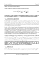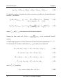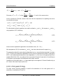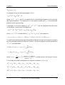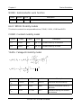
1
Software Package for Two-Dimensional Process and Device Simulation Version 4.0 for Windows User’s Manual Siborg Systems Inc Copyright ©1994, 95, 96, 97, 98 by Siborg Systems Inc. All Rights Reserved. First Printing January 1998. Photocopying or any other reproduction of any part of this document violates copyright law. Additional copies of this document are available from the publisher: Siborg Systems Inc. 24 Combermere Cres. Waterloo, Ontario N2L 5B1 CANADA Phone FAX E-mail Web (519) 888-9906 (519) 725-9522 [email protected] http://www.siborg.ca Trademarks TM MicroTecTM, SiDif , MergICTM, SemSimTM, and SibGraf Inc. TM are trademarks of Siborg Systems Microsoft, MS-DOS are registered trademarks of Microsoft Corporation IBM is a registered trademark of International Business Machines Corporation. Chapter Table of Contents 1. Getting Started . . . . . . . . . . . . . . . . . . . . . . . . . . . . . . . . . . . . . . . . . . . . . . . . . . . . . . . . . 7 1.1 Introduction . . . . . . . . . . . . . . . . . . . . . . . . . . . . . . . . . . . . . . . . . . . . . . . . . . . . . . . . 9 1.1.1. MicroTec: The Semiconductor TCAD Calculator . . . . . . . . . . . . . . . . . . . . . . 9 1.1.2. Technical Parameters . . . . . . . . . . . . . . . . . . . . . . . . . . . . . . . . . . . . . . . . . . . . 10 1.2 Installing MicroTec . . . . . . . . . . . . . . . . . . . . . . . . . . . . . . . . . . . . . . . . . . . . . . . . . . 10 1.3 Quick start . . . . . . . . . . . . . . . . . . . . . . . . . . . . . . . . . . . . . . . . . . . . . . . . . . . . . . . . . 11 2. MicroTec User Interface . . . . . . . . . . . . . . . . . . . . . . . . . . . . . . . . . . . . . . . . . . . . . . . . . . 13 2.1 Introduction . . . . . . . . . . . . . . . . . . . . . . . . . . . . . . . . . . . . . . . . . . . . . . . . . . . . . . . . 15 2.2 Running MicroTec . . . . . . . . . . . . . . . . . . . . . . . . . . . . . . . . . . . . . . . . . . . . . . . . . . . 15 2.2.1. Select Project page . . . . . . . . . . . . . . . . . . . . . . . . . . . . . . . . . . . . . . . . . . . . . . 15 2.2.2. Project Settings Page . . . . . . . . . . . . . . . . . . . . . . . . . . . . . . . . . . . . . . . . . . . . . 16 3. MicroTec Graphics: SibGraf . . . . . . . . . . . . . . . . . . . . . . . . . . . . . . . . . . . . . . . . . . . . . . 19 3.1 Introduction . . . . . . . . . . . . . . . . . . . . . . . . . . . . . . . . . . . . . . . . . . . . . . . . . . . . . . . . 21 3.2 SibGraf 2D Output . . . . . . . . . . . . . . . . . . . . . . . . . . . . . . . . . . . . . . . . . . . . . . . . . . . 21 File . . . . . . . . . . . . . . . . . . . . . . . . . . . . . . . . . . . . . . . . . . . . . . . . . . . . . . . . . . . . . 21 Plot . . . . . . . . . . . . . . . . . . . . . . . . . . . . . . . . . . . . . . . . . . . . . . . . . . . . . . . . . . . . . 22 View. . . . . . . . . . . . . . . . . . . . . . . . . . . . . . . . . . . . . . . . . . . . . . . . . . . . . . . . . . . . 23 Annotate. . . . . . . . . . . . . . . . . . . . . . . . . . . . . . . . . . . . . . . . . . . . . . . . . . . . . . . . . 23 Help . . . . . . . . . . . . . . . . . . . . . . . . . . . . . . . . . . . . . . . . . . . . . . . . . . . . . . . . . . . . 23 2D Status Bar . . . . . . . . . . . . . . . . . . . . . . . . . . . . . . . . . . . . . . . . . . . . . . . . . . . . . 24 2D Tool Bar . . . . . . . . . . . . . . . . . . . . . . . . . . . . . . . . . . . . . . . . . . . . . . . . . . . . . . 24 2D Data File Structure . . . . . . . . . . . . . . . . . . . . . . . . . . . . . . . . . . . . . . . . . . . . . . 24 3.3 SibGraf Map/Edit Menu. . . . . . . . . . . . . . . . . . . . . . . . . . . . . . . . . . . . . . . . . . . . . . . 25 File . . . . . . . . . . . . . . . . . . . . . . . . . . . . . . . . . . . . . . . . . . . . . . . . . . . . . . . . . . . . . 25 Plot . . . . . . . . . . . . . . . . . . . . . . . . . . . . . . . . . . . . . . . . . . . . . . . . . . . . . . . . . . . . . 25 View. . . . . . . . . . . . . . . . . . . . . . . . . . . . . . . . . . . . . . . . . . . . . . . . . . . . . . . . . . . . 26 Annotate. . . . . . . . . . . . . . . . . . . . . . . . . . . . . . . . . . . . . . . . . . . . . . . . . . . . . . . . . 26 Help . . . . . . . . . . . . . . . . . . . . . . . . . . . . . . . . . . . . . . . . . . . . . . . . . . . . . . . . . . . . 26 Map Set Contours . . . . . . . . . . . . . . . . . . . . . . . . . . . . . . . . . . . . . . . . . . . . . . . . . 26 Map Status Bar. . . . . . . . . . . . . . . . . . . . . . . . . . . . . . . . . . . . . . . . . . . . . . . . . . . . 27 Map Tool Bar. . . . . . . . . . . . . . . . . . . . . . . . . . . . . . . . . . . . . . . . . . . . . . . . . . . . . 27 3.4 SibGraf 3D Output . . . . . . . . . . . . . . . . . . . . . . . . . . . . . . . . . . . . . . . . . . . . . . . . . . . 28 File . . . . . . . . . . . . . . . . . . . . . . . . . . . . . . . . . . . . . . . . . . . . . . . . . . . . . . . . . . . . . 28 Plot . . . . . . . . . . . . . . . . . . . . . . . . . . . . . . . . . . . . . . . . . . . . . . . . . . . . . . . . . . . . . 28 View. . . . . . . . . . . . . . . . . . . . . . . . . . . . . . . . . . . . . . . . . . . . . . . . . . . . . . . . . . . . 29 Annotate. . . . . . . . . . . . . . . . . . . . . . . . . . . . . . . . . . . . . . . . . . . . . . . . . . . . . . . . . 29 Help . . . . . . . . . . . . . . . . . . . . . . . . . . . . . . . . . . . . . . . . . . . . . . . . . . . . . . . . . . . . 29 3D Status Bar . . . . . . . . . . . . . . . . . . . . . . . . . . . . . . . . . . . . . . . . . . . . . . . . . . . . . 29 3D Tool Bar . . . . . . . . . . . . . . . . . . . . . . . . . . . . . . . . . . . . . . . . . . . . . . . . . . . . . . 29 3.5 Annotate . . . . . . . . . . . . . . . . . . . . . . . . . . . . . . . . . . . . . . . . . . . . . . . . . . . . . . . . . . . 30 3.6 Zooming . . . . . . . . . . . . . . . . . . . . . . . . . . . . . . . . . . . . . . . . . . . . . . . . . . . . . . . . . . . 30 3.7 Directives . . . . . . . . . . . . . . . . . . . . . . . . . . . . . . . . . . . . . . . . . . . . . . . . . . . . . . . . . . 30 4. Process Simulation . . . . . . . . . . . . . . . . . . . . . . . . . . . . . . . . . . . . . . . . . . . . . . . . . . . . . . 33 4.1 Introduction . . . . . . . . . . . . . . . . . . . . . . . . . . . . . . . . . . . . . . . . . . . . . . . . . . . . . . . . 35 MICROTEC-4.0 User’s Manual 3 Chapter 4.2 Physical model . . . . . . . . . . . . . . . . . . . . . . . . . . . . . . . . . . . . . . . . . . . . . . . . . . . . . . 35 4.2.1. Diffusion coefficient . . . . . . . . . . . . . . . . . . . . . . . . . . . . . . . . . . . . . . . . . . . . . 36 4.2.2. Oxidation enhanced diffusion . . . . . . . . . . . . . . . . . . . . . . . . . . . . . . . . . . . . . . 37 4.2.3. Analytical oxidation model . . . . . . . . . . . . . . . . . . . . . . . . . . . . . . . . . . . . . . . . 37 4.2.4. Segregation . . . . . . . . . . . . . . . . . . . . . . . . . . . . . . . . . . . . . . . . . . . . . . . . . . . . 38 4.2.5. Ion implantation . . . . . . . . . . . . . . . . . . . . . . . . . . . . . . . . . . . . . . . . . . . . . . . . 39 4.3 Simulation algorithm . . . . . . . . . . . . . . . . . . . . . . . . . . . . . . . . . . . . . . . . . . . . . . . . . 40 4.4 References . . . . . . . . . . . . . . . . . . . . . . . . . . . . . . . . . . . . . . . . . . . . . . . . . . . . . . . . . 40 4.5 Running SiDif. . . . . . . . . . . . . . . . . . . . . . . . . . . . . . . . . . . . . . . . . . . . . . . . . . . . . . . 42 4.6 SiDif input file . . . . . . . . . . . . . . . . . . . . . . . . . . . . . . . . . . . . . . . . . . . . . . . . . . . . . . 42 4.6.1. SiDif Directive List . . . . . . . . . . . . . . . . . . . . . . . . . . . . . . . . . . . . . . . . . . . . . . 42 4.7 SiDif basic directives . . . . . . . . . . . . . . . . . . . . . . . . . . . . . . . . . . . . . . . . . . . . . . . . . 43 MESH: computational domain and mesh parameters . . . . . . . . . . . . . . . . . . . . . . 43 SUBS: substrate parameters. . . . . . . . . . . . . . . . . . . . . . . . . . . . . . . . . . . . . . . . . . 44 SOLV: numerical solution control. . . . . . . . . . . . . . . . . . . . . . . . . . . . . . . . . . . . . 44 PHDE: phosphorus deposition. . . . . . . . . . . . . . . . . . . . . . . . . . . . . . . . . . . . . . . . 45 BODE: boron deposition . . . . . . . . . . . . . . . . . . . . . . . . . . . . . . . . . . . . . . . . . . . . 45 ASDE: arsenic deposition . . . . . . . . . . . . . . . . . . . . . . . . . . . . . . . . . . . . . . . . . . . 45 PHIM: phosphorus implant . . . . . . . . . . . . . . . . . . . . . . . . . . . . . . . . . . . . . . . . . . 45 BOIM: boron implant . . . . . . . . . . . . . . . . . . . . . . . . . . . . . . . . . . . . . . . . . . . . . . 46 ASIM: arsenic implant. . . . . . . . . . . . . . . . . . . . . . . . . . . . . . . . . . . . . . . . . . . . . . 46 OXID: oxidation parameters . . . . . . . . . . . . . . . . . . . . . . . . . . . . . . . . . . . . . . . . . 46 ANNE: annealing parameters . . . . . . . . . . . . . . . . . . . . . . . . . . . . . . . . . . . . . . . . 46 EPIT: epi-layer formation . . . . . . . . . . . . . . . . . . . . . . . . . . . . . . . . . . . . . . . . . . . 47 4.8 SiDif model parameter directives. . . . . . . . . . . . . . . . . . . . . . . . . . . . . . . . . . . . . . . . 48 BAND: Bandgap and intrinsic carrier concentration. . . . . . . . . . . . . . . . . . . . . . . 48 DIFF: Diffusivity of Arsenic, Boron and Phosphorus . . . . . . . . . . . . . . . . . . . . . . 48 OED: Oxidation-enhanced diffusion . . . . . . . . . . . . . . . . . . . . . . . . . . . . . . . . . . . 49 4.8.1. Deal-Grove oxidation kinetic constants . . . . . . . . . . . . . . . . . . . . . . . . . . . . . . 49 DROX: Dry oxidation kinetic constants . . . . . . . . . . . . . . . . . . . . . . . . . . . . . . . . 50 WEOX: Wet oxidation kinetic constants. . . . . . . . . . . . . . . . . . . . . . . . . . . . . . . . 50 LOCO: Local oxidation “bird’s beak” formula parameters. . . . . . . . . . . . . . . . . . 51 SEGR: Segregation parameters . . . . . . . . . . . . . . . . . . . . . . . . . . . . . . . . . . . . . . . 52 4.9 Examples of SiDif input files . . . . . . . . . . . . . . . . . . . . . . . . . . . . . . . . . . . . . . . . . . . 52 4.9.1. MOSFET fragment . . . . . . . . . . . . . . . . . . . . . . . . . . . . . . . . . . . . . . . . . . . . . . 52 4.9.2. LDD MOSFET fragment. . . . . . . . . . . . . . . . . . . . . . . . . . . . . . . . . . . . . . . . . . 53 4.9.3. Fragment with LOCOS . . . . . . . . . . . . . . . . . . . . . . . . . . . . . . . . . . . . . . . . . . . 53 4.9.4. Doping by deposition . . . . . . . . . . . . . . . . . . . . . . . . . . . . . . . . . . . . . . . . . . . . 53 4.9.5. Buried layer and epitaxy . . . . . . . . . . . . . . . . . . . . . . . . . . . . . . . . . . . . . . . . . . 54 4.9.6. Emitter region . . . . . . . . . . . . . . . . . . . . . . . . . . . . . . . . . . . . . . . . . . . . . . . . . . 54 5. Device formation . . . . . . . . . . . . . . . . . . . . . . . . . . . . . . . . . . . . . . . . . . . . . . . . . . . . . . . 57 5.1 Introduction . . . . . . . . . . . . . . . . . . . . . . . . . . . . . . . . . . . . . . . . . . . . . . . . . . . . . . . . 59 5.2 Running MergIC. . . . . . . . . . . . . . . . . . . . . . . . . . . . . . . . . . . . . . . . . . . . . . . . . . . . . 59 5.3 MergIC input file . . . . . . . . . . . . . . . . . . . . . . . . . . . . . . . . . . . . . . . . . . . . . . . . . . . . 59 5.3.1. MESH: Domain and mesh. . . . . . . . . . . . . . . . . . . . . . . . . . . . . . . . . . . . . . . . . 60 5.3.2. FRAG: fragment description . . . . . . . . . . . . . . . . . . . . . . . . . . . . . . . . . . . . . . . 60 4 MICROTEC-4.0 User’s Manual Chapter 5.4 Examples of MergIC input file. . . . . . . . . . . . . . . . . . . . . . . . . . . . . . . . . . . . . . . . . . 61 5.4.1. Viewing a fragment . . . . . . . . . . . . . . . . . . . . . . . . . . . . . . . . . . . . . . . . . . . . . . 61 5.4.2. Symmetrical device using one fragment . . . . . . . . . . . . . . . . . . . . . . . . . . . . . . 61 5.4.3. Vertical BJT with substrate collector . . . . . . . . . . . . . . . . . . . . . . . . . . . . . . . . 61 5.4.4. Vertical BJT with a buried layer . . . . . . . . . . . . . . . . . . . . . . . . . . . . . . . . . . . . 62 5.4.5. I2L Device. . . . . . . . . . . . . . . . . . . . . . . . . . . . . . . . . . . . . . . . . . . . . . . . . . . . . 62 6. Device Simulation. . . . . . . . . . . . . . . . . . . . . . . . . . . . . . . . . . . . . . . . . . . . . . . . . . . . . . . 63 6.1 Introduction . . . . . . . . . . . . . . . . . . . . . . . . . . . . . . . . . . . . . . . . . . . . . . . . . . . . . . . . 65 6.2 Basic System of Equations . . . . . . . . . . . . . . . . . . . . . . . . . . . . . . . . . . . . . . . . . . . . . 65 6.2.1. Bandgap narrowing . . . . . . . . . . . . . . . . . . . . . . . . . . . . . . . . . . . . . . . . . . . . . . 65 6.2.2. SRH and Auger Recombination and Impact Ionization . . . . . . . . . . . . . . . . . . 66 6.2.3. Surface Recombination . . . . . . . . . . . . . . . . . . . . . . . . . . . . . . . . . . . . . . . . . . . 67 6.2.4. Boundary Conditions. . . . . . . . . . . . . . . . . . . . . . . . . . . . . . . . . . . . . . . . . . . . . 67 6.2.5. Mobility Models . . . . . . . . . . . . . . . . . . . . . . . . . . . . . . . . . . . . . . . . . . . . . . . . 69 6.3 Numerical technique. . . . . . . . . . . . . . . . . . . . . . . . . . . . . . . . . . . . . . . . . . . . . . . . . . 70 6.3.1. Finite-Difference Scheme . . . . . . . . . . . . . . . . . . . . . . . . . . . . . . . . . . . . . . . . . 71 6.3.2. Modified linearization of the discretized Poisson equation . . . . . . . . . . . . . . . 73 6.3.3. Initial guess strategy . . . . . . . . . . . . . . . . . . . . . . . . . . . . . . . . . . . . . . . . . . . . . 74 6.4 References . . . . . . . . . . . . . . . . . . . . . . . . . . . . . . . . . . . . . . . . . . . . . . . . . . . . . . . . . 76 6.5 Running SemSim . . . . . . . . . . . . . . . . . . . . . . . . . . . . . . . . . . . . . . . . . . . . . . . . . . . . 77 6.6 SemSim input file. . . . . . . . . . . . . . . . . . . . . . . . . . . . . . . . . . . . . . . . . . . . . . . . . . . . 78 6.6.1. SemSim list of directives. . . . . . . . . . . . . . . . . . . . . . . . . . . . . . . . . . . . . . . . . . 78 #BAS: Basic directives . . . . . . . . . . . . . . . . . . . . . . . . . . . . . . . . . . . . . . . . . . . . . 78 #DOP: Analytical doping data . . . . . . . . . . . . . . . . . . . . . . . . . . . . . . . . . . . . . . . . 78 #ELE: Electrodes . . . . . . . . . . . . . . . . . . . . . . . . . . . . . . . . . . . . . . . . . . . . . . . . . . 78 #IVD: IV-data or a set of IV-curves . . . . . . . . . . . . . . . . . . . . . . . . . . . . . . . . . . . 78 #MAT: Material Properties . . . . . . . . . . . . . . . . . . . . . . . . . . . . . . . . . . . . . . . . . . 78 #MOB: Mobility models . . . . . . . . . . . . . . . . . . . . . . . . . . . . . . . . . . . . . . . . . . . . 79 #REC: Recombination parameters. . . . . . . . . . . . . . . . . . . . . . . . . . . . . . . . . . . . . 79 #IMP: Impact ionization . . . . . . . . . . . . . . . . . . . . . . . . . . . . . . . . . . . . . . . . . . . . 79 #PHO: Photogeneration . . . . . . . . . . . . . . . . . . . . . . . . . . . . . . . . . . . . . . . . . . . . . 79 6.6.2. #BAS: Basic directives . . . . . . . . . . . . . . . . . . . . . . . . . . . . . . . . . . . . . . . . . . . 79 MESH: Domain and mesh parameters. . . . . . . . . . . . . . . . . . . . . . . . . . . . . . . . . . 80 SOLV: Computation control . . . . . . . . . . . . . . . . . . . . . . . . . . . . . . . . . . . . . . . . . 80 MODE: Model options . . . . . . . . . . . . . . . . . . . . . . . . . . . . . . . . . . . . . . . . . . . . . 81 6.6.3. #DOP: Analytical doping data . . . . . . . . . . . . . . . . . . . . . . . . . . . . . . . . . . . . . 81 DOPA: Doping well. . . . . . . . . . . . . . . . . . . . . . . . . . . . . . . . . . . . . . . . . . . . . . . . 81 DOPN: Numerical doping data . . . . . . . . . . . . . . . . . . . . . . . . . . . . . . . . . . . . . . . 82 6.6.4. #OXI: Oxide . . . . . . . . . . . . . . . . . . . . . . . . . . . . . . . . . . . . . . . . . . . . . . . . . . . 82 OXID: Oxide region . . . . . . . . . . . . . . . . . . . . . . . . . . . . . . . . . . . . . . . . . . . . . . . 82 6.6.5. #REM: Remesh . . . . . . . . . . . . . . . . . . . . . . . . . . . . . . . . . . . . . . . . . . . . . . . . . 83 REME: Remesh region . . . . . . . . . . . . . . . . . . . . . . . . . . . . . . . . . . . . . . . . . . . . . 83 6.6.6. #ELE: Electrode directive . . . . . . . . . . . . . . . . . . . . . . . . . . . . . . . . . . . . . . . . . 83 OHMI: Ohmic electrode . . . . . . . . . . . . . . . . . . . . . . . . . . . . . . . . . . . . . . . . . . . . 83 GATE: Gate electrode . . . . . . . . . . . . . . . . . . . . . . . . . . . . . . . . . . . . . . . . . . . . . . 84 SCHO: Schottky electrode. . . . . . . . . . . . . . . . . . . . . . . . . . . . . . . . . . . . . . . . . . . 84 MICROTEC-4.0 User’s Manual 5 Chapter 6.6.7. #IVD: IV-data directive. . . . . . . . . . . . . . . . . . . . . . . . . . . . . . . . . . . . . . . . . . . 85 IVDA: IV-Curve . . . . . . . . . . . . . . . . . . . . . . . . . . . . . . . . . . . . . . . . . . . . . . . . . . 85 6.6.8. #MAT: Material properties . . . . . . . . . . . . . . . . . . . . . . . . . . . . . . . . . . . . . . . . 85 BAND: Temperature and bandgap parameters . . . . . . . . . . . . . . . . . . . . . . . . . . . 85 PERM: Dielectric permittivity. . . . . . . . . . . . . . . . . . . . . . . . . . . . . . . . . . . . . . . . 86 WORK: Semiconductor work function . . . . . . . . . . . . . . . . . . . . . . . . . . . . . . . . . 87 6.6.9. #MOB: Mobility models . . . . . . . . . . . . . . . . . . . . . . . . . . . . . . . . . . . . . . . . . . 87 CONM: Constant mobility model . . . . . . . . . . . . . . . . . . . . . . . . . . . . . . . . . . . . . 87 YAMA: Yamaguchi mobility model . . . . . . . . . . . . . . . . . . . . . . . . . . . . . . . . . . . 87 LOMB: Lombardi surface mobility model . . . . . . . . . . . . . . . . . . . . . . . . . . . . . . 88 BIPO: Bipolar mobility model. . . . . . . . . . . . . . . . . . . . . . . . . . . . . . . . . . . . . . . . 90 6.6.10. #REC: Recombination parameters . . . . . . . . . . . . . . . . . . . . . . . . . . . . . . . . . 92 SRH: Shockley-Read-Hall recombination parameters . . . . . . . . . . . . . . . . . . . . . 92 AUGE: Auger recombination parameters . . . . . . . . . . . . . . . . . . . . . . . . . . . . . . . 93 SURF: Surface recombination parameters . . . . . . . . . . . . . . . . . . . . . . . . . . . . . . 93 RADI: Radiative recombination parameters . . . . . . . . . . . . . . . . . . . . . . . . . . . . . 94 6.6.11. #IMP: Impact Ionization . . . . . . . . . . . . . . . . . . . . . . . . . . . . . . . . . . . . . . . . . 94 IONE: Impact ionization exponent . . . . . . . . . . . . . . . . . . . . . . . . . . . . . . . . . . . . 94 IONP: Impact ionization coefficient . . . . . . . . . . . . . . . . . . . . . . . . . . . . . . . . . . . 95 6.6.12. #PHO: Photogeneration. . . . . . . . . . . . . . . . . . . . . . . . . . . . . . . . . . . . . . . . . . 96 PHOT: Photogeneration well. . . . . . . . . . . . . . . . . . . . . . . . . . . . . . . . . . . . . . . . . 96 6 MICROTEC-4.0 User’s Manual GETTING STARTED MICROTEC-4.0 User’s Manual 7 Getting Started Chapter 1 1.1. Introduction Semiconductor device modeling has become a standard design tool in the microelectronics industry. A few years ago this modeling was performed primarily on supercomputers. At the present time a number of commercial 2D process and device simulators are available, mostly for UNIX based workstations. Normally they require tens of Mbytes of memory even for modest sized meshes. Increasing performance and widespread availability of IBM PCs and compatibles encourage the development of software tools that can be used for 2D modeling of semiconductor devices and processes with a rather low memory capacity and speed of computation. Recently a few efficient programs were developed for two-dimensional semiconductor process-device simulation on a PC which have now been integrated together into a package named MicroTec. MicroTec: The Semiconductor TCAD Calculator MicroTec allows 2D silicon process modeling including implantation, diffusion and oxidation and 2D steady-state semiconductor device simulation like MOSFET, DMOS, JFET, BJT, IGBT, Schottky, photosensitive devices etc. Although MicroTec is significantly simplified compared to widely available commercial simulators, it nevertheless is a very powerful modeling tool for industrial semiconductor process/device design. In many instances MicroTec outperforms existing commercial tools and it is remarkably robust and easy-to-use. MicroTec is especially attractive for educational purposes due to its completeness and ease of use. It enables development of a set of problems for a tutorial in semiconductor device physics with minimal effort. The goal of such a computer-aided course would be to teach students basic ideas about modern semiconductor device design. A flexible and easy-to use graphic interface allows the user to output results of the process/device simulation on essentially any printer or plotter or into a file. Despite its apparent simplicity, MicroTec covers all the basic needs of semiconductor process/ device design complemented with efficient and flexible graphics tools. It is much easier to use than any other tool of its kind. MicroTec is a must for those who want to understand physics of semiconductor devices without knowing much about computers or numerical methods and who do not have much time for learning new process/device simulation tools. MicroTec is an excellent tool for managers, R&D engineers, students, professors and researchers and can be referred to as a TCAD calculator. MicroTec is based on the diffusion-drift model and the present version does not include energy balance. It employs the finite-difference technique on a rectangular, auto-adjusting mesh. Only steady-state analysis is available in the present version of MicroTec. Physical models (mobility, life time, recombination and impact ionization) implemented in MicroTec are essentially the same as those used in the widely used commercial simulators. MICROTEC-4.0 User’s Manual 9 Getting Started Chapter 1 Technical Parameters MicroTec-4.0 is a true 32-bit Windows application and can be run on any PC-386 or higher. MicroTec-4.0 uses dynamic memory allocation. There is no memory threshold so it can be used even on a computer with only 1 Mbyte memory if the mesh size is not larger than about 2,000 nodes. Other commercially available tools typically require about 20 Mbyte memory for a mesh size limited to 3,500 nodes. MicroTec-4.0 device simulation tools require about 8 Mbytes of memory for a 20,000 node mesh. Typical CPU time for one IV point is less than 1 minute on a PC/486 when using 1,000 nodes. For the process simulation tool, about 4 Mbytes of memory is required for a 20,000 node mesh. Simulation of a typical technological route requires 1-10 minute CPU time on a PC/486. The most remarkable features of MicroTec are: dramatically reduced memory requirements, absolute numerical stability (almost arbitrary changes of contact voltages, even with impact ionization), high speed and very easy-to-use Graphical User Interface. 1.2. Installing MicroTec Read about the latest changes in the Installation procedure in the readme.txt file on the installation Disk. You will need about 4 Megabytes of disk space to install MicroTec-4.0. 1. Create directory C:\MT305 on a hard disk 2. Copy all MicroTec files from the floppy into this directory 3. Open DOS window, change your current directory to C:\MT305 and extract MicroTec components using the command pkunzip mt305.zip 4. Register you computer using "install" command at the command prompt (you will need the serial number from file serial_n.txt on the floppy or request one from [email protected]) install /0 File "inst.pas" will be created. Please zip this file and E-mail the zipped archive to [email protected] as an attachment by E-mail. We will then register your computer and send you another "inst.pas" file. Please include the name of the contact person, phone and Fax numbers to facilitate communication should it be required. Keep a copy of the "inst.pas" at all times. 5. Unzip received "inst.pas" in the MT305 directory and run install /i This will complete the installation procedure You may run MicroTec without registering it. In this case it will run in a demonstration mode where you can run any process simulation in a fixed domain 0.7 by 0.7 microns. You will also be able to simulate an NMOSFET with 1 um Leff and Tox of 0.02 um. You cannot 10 MICROTEC-4.0 User’s Manual Getting Started Chapter 1 change the transistor structure, e.g. location of electrodes, doping distribution and the domain size, but you can change the voltages, number of nodes, model parameters etc. Without registration, for all other device simulation examples included in the distribution package you can only plot the output results and edit the input data. Do not try to run these examples because the doping distribution and geometry of the simulated device will still be that of the NMOSFET. 1.3. Quick start Select a project in the project list window on the ‘Select Project’ tab, by clicking the left mouse button on the project name, see ’Figure 2.1 Select Project tab.’ on page 16. The corresponding simulator name will be shown in the ‘Method’ window. The simulator name may be: SiDif, MergIC, SemSim or Batch for the process simulation, generation of the device structure, device simulation or a batch mode simulation respectively. In the batch mode you may run several jobs using different tools, for example, a process simulation, a generation of the final device structure using MergIC and then a device simulation for the generated device with a number of different IV curves. To modify the project settings click on the ‘Project Settings’ tab, see ’Figure 2.2 Project Settings tab.’ on page 17. Another page of the main MicroTec window will appear showing a directives, subdirectives and parameters tree. Click on a folder symbol to open it. Double-click a parameter to edit it. If you click on a directive or subdirective with the left and then the right mouse button, a context sensitive menu appears allowing ‘Delete’, ‘Copy’, ‘Insert Directive’ or ‘Insert Subdirective’, ‘Add Subdirective’ and ‘Add Parameter’. If while a subdirective is selected you select ‘Add Parameter’, a list of available parameters pops up. Select an item and click OK. If you click on ‘Add Subdirective’ or ‘Insert Directive’ a list of available directives or subdirectives pops up. Select an item and click ‘OK’. A brief description of the directives, subdirectives and parameters is given in the selection windows. A more detailed description may be found in later chapters, where each simulator is described in detail. The most convenient way of starting a new project is to go to the ‘Select Project’ window, select an existing project similar to the desired one and then click the ‘Copy’ button. A new project will be created with “(copy)” appended to the old project name. Edit the name in the ‘Name’ window and click the ‘Update’ button. To modify directives/parameters, switch to the “Project Settings” page as described above. If you need to start a new project, type the name of the project in the ‘Name’ window, select a method in the ‘Method’ window and click the ‘Add’ button. A project with default directive/ parameter settings will be created. Change the current page to ‘Project Settings’ and edit the parameters as described above. To run a simulation click the ‘Run’ button. After the simulation is complete you may display the results by clicking on the ‘2D Output’ or ‘3D Output’ buttons for plotting I-V curves or 3D/ colour map plots of two-dimensional distributions respectively. Click on Plot/Add... or Plot/ Select... for ‘2D Output’ or ‘3D Output’ respectively to plot an IV-curve or a surface. MICROTEC-4.0 User’s Manual 11 Getting Started Chapter 1 The 2D distributions available for plotting are: electrostatic potential, carrier and current densities, Fermi quasi-potentials, electric field components, etc. You may also plot 2D cross-sections and IV-plots as well as transconductances as a function of applied voltage. For more information on the Graphics Tools refer to Chapter 3. 12 MICROTEC-4.0 User’s Manual MICROTEC USER INTERFACE MICROTEC-4.0 User’s Manual 13 MicroTec User Interface Chapter 2 2.1. Introduction MicroTec is a shell integrating four programs for silicon process-device simulation: • SiDif- two-dimensional SImulator for DIFfusion and oxidation • MergIC- program for MERGing fragments of IC elements • SemSim- two-dimensional steady-state SEMiconductor device SIMulator • SibGraf- interactive 3D and 2D graphics MicroTec is a highly robust 2D semiconductor process-device simulation package which can be run on IBM PCs and compatibles with a reasonable CPU time and low memory requirements. 2.2. Running MicroTec The MicroTec main menu has two tabbed windows: ‘Select Project’ and ‘Project Settings’, that can be viewed by clicking on the named tab. Select Project page The first page of the MicroTec main menu, called ‘Select Project’ shown in figure 2.1, comprises the following: • Run Bar with ‘Run’, ‘Edit’, ‘2D Output’, ‘3D Output’, ‘Help’ and ‘Exit’ buttons. • Name Text Box showing the current project name. • Method Text Box showing the simulator used for the current project. • Project List Window showing the list of available projects. • Project Description Window with a brief description of the current project. • Method Description Window with a brief description of the current project simulator. • Project Handling Bar with ‘Add’, ‘Update’, ‘Copy’ and ‘Delete’ buttons. To select a project in the project list window on the ‘Select Project’ page, click the left mouse button on a project name. The corresponding project and simulator name as well as project description will appear in the ‘Name’ and ‘Method’ text boxes and ‘Description’ window respectively. If you need to change a project name or project description, edit the text in the appropriate window and click the ‘Update’ button. If you need to start a new project, type a project name in the ‘Name’ window, select a method in the ‘Method’ text box and click the ‘Add’ button. A project with default settings will be created. Change the current page to the ‘Project Settings’ page and edit the parameters as described in the Section Project Settings Page on page 16. When you start a new project, you will need to select the appropriate ‘Method’ in the ‘Method’ MICROTEC-4.0 User’s Manual 15 MicroTec User Interface Chapter 2 window. The following four options are available: • SiDif- two-dimensional SImulation of implantation, diffusion and oxidation • MergIC- program for MERGing fragments simulated by SiDif • SemSim- two-dimensional steady-state semiconductor device simulation • Batch- batch mode simulation of any number of process and/or device simulations Another way of starting a new project is to copy an existing project. Select a project and click the ‘Copy’ button. A new project with ‘(copy)’ appended to it’s name will be created. To modify the project name, change the name in the ‘Name’ text box and click the ‘Update’ button in the main MicroTec window. Switch to the ‘Project Settings’ page and change the parameters as needed. To run a simulation, click the Figure 2.1 Select Project tab. ‘Run’ button. After the simulation is complete you may display the results by clicking on the ‘2D Output’ or ‘3D Output’ buttons for plotting IV curves or 3D/contour plots of two-dimensional distributions of various variables such as electrostatic potential, carrier and current densities, Fermi quasi-potentials, electric field components, etc. See Section MicroTec Graphics: SibGraf on page 31 for more information on the MicroTec graphics. Project Settings Page To modify project settings click on the ‘Project Settings’ tab. The other page of the main MicroTec menu will appear showing a Project Tree containing directives, subdirectives and parameters, as in figure 2.2. Click the left mouse button on a folder symbol to open it. Double-click the left mouse button on a parameter to edit it. To modify the tree structure, click a directive/subdirective/parameter with the left and then the right mouse button. A menu pops up allowing you to ‘Delete’, ‘Copy’, ‘Insert’ or ‘Add’ an entry. If you select ‘Delete’ the current entry will be deleted. If you select ‘Copy’, a new copy of the current entry will be added at the end of the project tree. Selecting ‘Insert’ or ‘Add’ brings up a new window showing a list of entries that may be added at this stage. Select one of them and click ‘OK’. Newly added parameters are given default values. Double-clicking a parameter brings up an edit window showing the current parameter value and a brief parameter description. Edit the 16 MICROTEC-4.0 User’s Manual MicroTec User Interface Chapter 2 parameter value in the text box and click ‘OK’. Figure 2.2 Project Settings tab. Context sensitive menu is visible. There are different types of directives in MicroTec: unique or non-unique and mandatory or optional. For example, the ‘Photogeneration’ directive is optional and unique, one may skip this directive or give it a number of subdirectives to obtain several photogeneration wells. Alternatively, the ‘Basic’ directive is mandatory and unique. Any newly created project will contain all mandatory directives with parameters assigned default values. Mandatory directives cannot be deleted. MICROTEC-4.0 User’s Manual 17 MicroTec User Interface 18 Chapter 2 MICROTEC-4.0 User’s Manual MICROTEC GRAPHICS: SIBGRAF MICROTEC-4.0 User’s Manual 19 MicroTec Graphics: SibGraf Chapter 3 3.1. Introduction SibGraf is a fast and user-friendly software tool for plotting I-V curves and two-dimensional distributions of the electrostatic potential, carrier and current densities, Fermi quasi-potentials, generation rate and electric field components as well as several other functions. It is menu-driven and includes on-line help. SibGraf generates 3D plots, contour lines, color maps, 2D cross-sections of 3D plots and 2D plots for I-V data. 3.2. SibGraf 2D Output Figure 3.1 SibGraf 2D window. This function allows you to plot any column, a product of any two columns, or a ratio of any two columns as a function of any column in the 2D data file. The 2D data file is generated by SemSim and represents IV data and transconductance data. When you click on the ‘2D Output’ button in the main MicroTec window, a new window pops up with five menu choices: ‘File’, ‘Plot’, ‘View’, ‘Annotate’ and ‘Help’. The subtopics available under these menus are described below. To zoom in on a portion of the graph use the left mouse button as described in the section titled Zooming below. You may also use the Annotate command which is also described below. The Tool Bar buttons allow you to change the current point and curve, switch to and from logarithmic scale and delete the current curve, shown in yellow. More information is available in the Section 2D Tool Bar on page 24. File Open - Open a picture file, *.mtp, previously created by this program. Load - Load data from a file containing 2D data, e.g. IV curves. *.2d*. See “2D Data File Structure” on page 24. Save - Save the plot to the picture file, *.mtp, that is currently open. If there is no picture file that is currently open (if the Load function was used instead) then this function will behave as the ‘Save As’ function described below. Save As - Save the plot to a picture file, *.mtp. A window will be provided to allow you to choose the file name. Clear - Clear the plot window (delete all curves in the window). Print - Print the plot to a printer or to a PostScript file. MICROTEC-4.0 User’s Manual 21 MicroTec Graphics: SibGraf Chapter 3 Import Data - Allows you to add new data from a file to the graph. The file may contain a few curves. For every curve the first line for every subset of data includes the number of points in the curve and name of the curve, followed by two columns of data for X and Y axis respectively. Export Data - Allows you to transfer data from the graph into an ASCII file. See previous section for the file format. The file can then be imported using the Import Data command. New Window - Open new empty Sibgraf 2D window. Exit - Close the window. Plot Add - Open a window which displays the information about the current data file. A file must have been previously loaded with the ‘Load’ command under the ‘File’ submenu for this to work. A new window appears showing the information extracted from the data file which has been loaded. It enables the user to select curves to be shown in the plot window. The data labels are derived by appending the first letters of the Electrode name parameters to the predefined letters V (for voltage) and I (for current). The first line of this window shows the current family number and name and allows the user to switch between families. Odd family numbers correspond to IV data and even numbers correspond to transconductance data. The table contains names as well as maximum and minimum values of each column in the current family. The first two check boxes beside each column allow the user to choose which column will be the X axis and which will be the Y axis. The third check box allows the user to choose a column which will be multiplied by the column chosen as the Y axis. Figure 3.2 Plot/Add... menu. In this case a product of the respective elements of the two columns will be plotted. The fourth check box allows the user to choose a column which will be used as a divider for the Y axis. In this case a ratio of the respective elements of the two columns will be plotted. The setup necessary to plot current gain, β=IC/IB, is shown in figure 3.2. The user can type the name of the curve being created into the ‘Curve Name’ box. The default curve name is the name of the column chosen as the Y axis. When all required information is selected (at least the X and Y axes must be given), the curve may be added to the plot Figure 3.3 The Curve Source window. by pressing the ‘Add’ button. Once all the desired curves have ben added, click ‘Close’ to return to the SibGraf 2D window. The data used to create a curve may be viewed later by selecting the Curve/Source... menu, which brings up the window shown in figure 3.3. 22 MICROTEC-4.0 User’s Manual MicroTec Graphics: SibGraf Chapter 3 Copy - Copy the current curve from the plot to the SibGraf clipboard. This feature, combined with Paste, is used to create compillations of curves. Paste - Add the curve from the SibGraf clipboard to the current plot. Delete - Delete the current (yellow) curve from the plot. Source - Open a window which shows the data source for the current curve. The curve name may be changed from this window. Line, Color, Marker - Allows changes to the corresponding attributes of the current curve. View Axis Limits - Allows setting the minimum and maximum values for x and y, see figure 3.4. Also allows selection of the vertical offset option. The vertical offset creates a space between the curve and the axis lines. Figure 3.4 Axis Limits window. Options - Opens a window where the user can assign labels for horizontal and vertical axes and the title for the plot, see figure 3.5. The user can also specify the lowest value of the logarithm function corresponding to an argument approaching zero. The Show Markers and Show Lines check boxes apply to all the curves in the window. Information in this window may be saved by pressing the ‘Save’ button. A file “setup.mt” will be created and the settings will be read every time a new SibGraf 2D window is opened. Grid, Legend - Switch grid and legend on and off. Figure 3.5 2D Options window. Tool Bar - Switch tool bar on and off. Status Bar - Switch status bar on and off. Zoom Out - Turn off zoom; can also be done with ESC key. Annotate See the Section Annotate on page 30. Help Index - Help index for SibGraf. About - Display SibGraf info. MICROTEC-4.0 User’s Manual 23 MicroTec Graphics: SibGraf Chapter 3 2D Status Bar The status bar is the strip at the bottom of the plot window. It shows the value of the X and Y coordinates for the current marker on the current curve. The current marker is shown in red. 2D Tool Bar The tool bar is the line of buttons just below the main menu and above the plot window. The first two buttons are used to change the current curve which is shown in yellow. Each click will change the current curve to the next curve. The curves are ordered in the sequence they were added/pasted. The first button cycles upward through the curves and the second cycles downward. This can also be done by using the up and down arrow keys on the keyboard. Figure 3.6 SibGraf 2D window showing The next two buttons change the currently selected point marker on the curve. The marker of the current point is red as in figure 3.6. The buttons move the red marker to the left and right respectively. This can also be done using the left and right arrow keys on the keyboard. The x and y value of the current marker is displayed in the status bar. The buttons ‘logX’, ‘logY’, ‘absX’ and ‘absY’ are used to switch to and from logarithmic and absolute scale on either the X or Y axis. The second last button, marked ‘Del’, deletes the selected curve from the plot. The last button switches into the tracer mode. When in tracer mode, two perpendicular lines follow the mouse along the curve. The status bar displays the x and y values of the intersection point of the two lines. This allows you to trace any part of the graph, including points that fall between markers, as in figure 3.2. 2D Data File Structure This section describes the format of a data file that can be loaded by the ‘Load’ selection under the File menu. By default the program looks for files with an extension of ‘*.2d*’, where * is any character. Each data file contains sets of data, which are referred to as ‘families’. Each family is a number of data columns, each with the same number of entries (rows). After the file is loaded, the user may choose which column is the X axis and which column or columns will be shown on the Y axis. The user may also choose to plot a product or ratio of any two columns on the Y axis. It allows plotting of such quantities as current gain β=IC/IB, etc. 24 MICROTEC-4.0 User’s Manual MicroTec Graphics: SibGraf Chapter 3 3.3. SibGraf Map/Edit Menu The user has five menu choices: ‘File‘, ‘Plot‘, ‘View‘, ‘Annotate’ and ‘Help’. The subtopics available under these menus are described below. File Open - Open a file containing a plot previously created and saved by this program, *.mtm. Load - Load data from a file containing 2D distribution data, *.3d*. Save - Save the plot to the picture file that is currently open. If there is no plot that is currently open (if the Load function was used instead) then this function will behave as the ‘Save As’ function described below. *.mtm Save As - Save the plot to a picture file. A window will be provided to allow you to choose the file name. Clear - Erase the plot that is currently in the plot window. Print - Print the plot that is currently in the plot window to a printer or to a PostScript file. Figure 3.7 SibGraf map window. Export Data - Allows you transfer information from ‘SibGraf Map’ into another file. Import Data - Allows you to add information to the ‘SibGraf Map’ window. New Window - Open a new empty SibGraf Map window. Exit - Close the window. Plot Source - Opens a window which shows the data source for the current plot. Select - Allows you to chose a variable to add to the SibGraf Map window, from a list of given variables. See figure 3.8. Figure 3.8 Plot/Surface... menu. If the current plot was invoked through the ‘Open’ function, ‘Source’ is the only subitem under ‘Surface’. If the file with 2D distribution data was loaded through the ‘Load’ function all surfaces contained in that file are listed after the item ‘Source’. Any of these surfaces may be plotted. MICROTEC-4.0 User’s Manual 25 MicroTec Graphics: SibGraf Chapter 3 View Axis Limits - Allows you to set minimum and maximum values for the x and y (vertical and horizontal axis). See figure 3.4. The vertical offset option is not available. Options - See Options in the Section View on page 23. Set Contours - See the Section Map Set Contours on page 26. Directives - Allows you to make the directives for the SibGraf Map/Edit windown visible. You can change the directives in the edit window, but not in the map window. If you are in the SibGraf Map window you may change the directives in the Projest Settings tab of the main menu. For more information see Section Directives on page 30 . Rainbow8, Rainbow16, BlackWhite, Contours - Each of these four items describes one of the possible four SibGraf Map representations: Map using 8 colors, Map using 16 colors, Map using 8 levels of gray and Contour Map. Grid, Legend - Show/hide discretization mesh and legend for Color Map. Tool bar, Status bar, AutoRedraw - Shows or hides the tool bar and status bar. Turns auto redraw on or off. With autoredraw on, the window will redraw itself automatically once a window covering it is moved. Redraw - Redraw current plot. Zoom Out - Turn off zoom; can also be done with ESC key. Annotate See section 3.5 ‘Annotate’. Help Index - Open a window with the help index. About - Displays SibGraf info. Map Set Contours The ‘Set Contours’ subitem under the ‘View’ menu item of the SibGraf Map window opens a window where the user can assign the levels at which the contour lines are drawn for the current surface. A contour map is shown in figure 3.9. Automatic - The user can assign the start and the step values for Z (or Log Z) and choose whether all or none of the contour labels are shown. Manual - The user can add a new contour line by pressing the ‘Add’ button and specifying Z (or Log Z) values for it, remove an existing contour line by choosing it in the table and pressing the 26 MICROTEC-4.0 User’s Manual MicroTec Graphics: SibGraf Chapter 3 ‘Remove’ button, or modify the existing contour lines by changing their Z (or Log Z) values. The check box in front of each level value indicates whether or not the contour labels for all contours at this level are shown. The user can also modify an existing contour line and its label by positioning the mouse on a particular label on the plot and pressing the right mouse button. A menu will appear through which the user can choose to remove either this label or all contour lines at the corresponding level from the plot. Figure 3.9 Contour map The location of a label can be changed by dragging the label with the left mouse button. If the label is moved completely out of the plot area it becomes invisible, although it still exists and will appear if, for example, the Unzoom function is used. A new contour line may be added to the graph by right clicking anywhere in the graph area. The new contour line will run through the point where the mouse was clicked. Right clicking on a contour label brings up a menu allowing the deletion of the label or of the entire contour line. Map Status Bar The status bar is the strip at the bottom of the plot window. If probe mode is off, the first row of three numbers in the status bar show the values of the X and Y coordinates of the current crosssections, and the Z value at the point of their intersection. If probe mode (see below) is on, the first row of three numbers show the values of the X, Y and Z coordinates at the current mouse position. The bottom row of numbers always show the mesh step numbers of the current X and Y crosssections and the overall dimension of the grid. Map Tool Bar The tool bar is the line of buttons just below the main menu and just above the plot window. The first four buttons are used to select current X and Y cross-sections. This can also be done by using the arrows on the keyboard. The ‘Log Z’ button is used to switch to and from a logarithmic scale of the Z coordinate. The next button opens a SibGraf 3D window displaying the current function. The next two buttons are used to plot the currently selected X and Y cross-sections in a separate SibGraf 2D window. All subsequent cross-section plots are added to the same SibGraf 2D window. The last button is the ‘Probe’ button. It is used to switch the probe mode on and off (see ‘Map Status Bar’ above). MICROTEC-4.0 User’s Manual 27 MicroTec Graphics: SibGraf Chapter 3 3.4. SibGraf 3D Output The user has five menu choices: ‘File’, ‘Plot’, ‘View’, ‘Annotate’ and ‘Help’. The subtopics available under these menus are described below. File Open - Open a picture file previously created and saved by this program, *.mts. Load - Load data from a file containing 2D distribution data, *.3d*. Save - Save the plot to the picture file that is currently open, *.mts. If there is no picture file that is currently open (if the Load function was used instead) then this function will behave as the ‘Save As’ function described below. Save As - Save the plot to a picture file. A window will be provided to allow you to choose the picture file name. Clear - Erase the plot that is currently in the plot window. Figure 3.10 SibGraf 3D window. Print - Print the plot that is currently in the plot window to a printer or to a PostScript file. Export Data - Allows you to transfer data from the graph into an ASCII file. See previous section for the file format. The file can then be imported using the Import Data command. Import Data - Allows you to add new data from a file to the graph. The file may contain a few curves. For every curve the first line for every subset of data includes the number of points in the curve and name of the curve, followed by two columns of data for X and Y axis respectively. New Window - Opens new Sibgraf 3D window. Exit - Close the SibGraf 3D window. Plot Source - Opens a window which shows the data source for the current surface. Fields cannot be edited. Select - gives you a variable list, figure 3.8, from which you can chose an item to plot on the graph. see figure 3.8. If the current plot was invoked through the Open function, “Source” is the only subitem under Surface. If the file with 2D distribution data was loaded through the ‘Load’ function, all the variables that may be displayed are contained in the file and are listed in the “Select” window. 28 MICROTEC-4.0 User’s Manual MicroTec Graphics: SibGraf Chapter 3 View Options - Opens a window where the user can assign labels for horizontal and vertical axes and the title for the plot. The user can also specify the lowest value of the logarithm function corresponding to an argument approaching zero. Tool bar, Status bar, AutoRedraw - allows you to make the toolbar and status bar visible or invisible. Turn auto redraw on and off. With autoredraw on, the window will redraw itself automatically once a window covering it is moved. Redraw - Redraw current surface. Zoom Out - Turns off zoom; can also be done with ESC key. Annotate See the Section Annotate on page 30. Help Index - Open a window with the help index. About - Display SibGraf info. 3D Status Bar The status bar is the strip at the bottom of the plot window. If probe mode is off, the first row of three numbers in the status bar show the values of the X and Y coordinates of the current crosssections, and the Z value at the point of their intersection. If probe mode (see below) is on, the first row of three numbers show the values of the X, Y and Z coordinates at the current mouse position. The bottom row of numbers always show the mesh step numbers of the current X and Y crosssections and the overall dimension of the grid. 3D Tool Bar The tool bar is the line of buttons just below the main menu and above the plot window. The first four buttons are used to rotate the surface about horizontal and vertical axes associated with the screen. The next four buttons are used to select different X and Y cross-sections. This can also be done by using the arrow keys on the keyboard. The button ‘Log Z’ is used to switch to and from a logarithmic scale. The third last button is used to open a SibGraf Map window displaying the current function. MICROTEC-4.0 User’s Manual 29 MicroTec Graphics: SibGraf Chapter 3 The last two buttons are used plot the currently selected X and Y cross-sections in a separate SibGraf 2D window. All subsequent cross-section plots are added to the same SibGraf 2D window. 3.5. Annotate All of the SibGraf 2D, 3D and Map windows have an Annotate item in their main menu. Two types of annotated objects may be created: Line and Text. Annotated objects are associated with the real X and Y coordinates and not with the window or screen position. Therefore, the annotation objects move with respect to the window when windows are zoomed or resized. When the subitem Line is chosen, the user can draw a line consisting of a number of straight segments. To continue a line from a point, click the left mouse button. To terminate an annotation line, click the right mouse button. To modify an existing Annotate Line object, first select it by clicking the left mouse button on the line. Then either the whole line or any of its nodes can be moved to the desired position with the left mouse button. Clicking the left mouse button anywhere away from the line will terminate the modification mode. When the subitem Text is chosen, a window will appear, where the user can type the required text and choose whether a border around the text is shown. When the OK button is pressed the text will be placed in the centre of the plot area. To move the existing Annotate Text object, first select it by clicking the left mouse button inside the text region. Then the text region can be moved to the desired position by dragging it with the left mouse button. If the content of the text object is to be changed, the user should first select the text object, then choose the subitem Edit under Annotate in the main menu. The user can delete annotation lines or text by selecting them as the current annotated object, as described above, and then choosing the subitem Delete under Annotate in the main menu. 3.6. Zooming The user may zoom in on a particular rectangle of any 2D, 3D or Map plot. Position the cursor over a point on the plot that you would like to use as the corner of a new plot. Press and hold the left mouse button as you move the mouse, which will show a rectangle on the plot corresponding to the area that will be shown on a new plot. When you have a rectangle defined that covers the area of the plot that you would like to zoom in on, release the mouse button and the plot will be replaced by a plot of the selected area. To restore the original plot you may press the ESC key or select ‘Zoom Out’ from the ‘View’ menu. In SibGraf 2D and Map windows you may unzoom the plot by selecting a rectangle outside the plotting area using the left mouse button. 3.7. Directives In both the SibGraf Map and SibGraf Edit windows under the View item in the main menu, there is an item called ‘Directives’. This item allows you to create directives in the window in which you are in. Directives are sections of the graph, which refer to specific sections listed in the project settings tab of the main window. You may change the directives in the SibGraf Edit window, by ... . Once you change the directives in the SibGraf Edit window and restart the program 30 MICROTEC-4.0 User’s Manual MicroTec Graphics: SibGraf Chapter 3 Figure 3.11 the directives will also change in the corresponding SibGraf Map window. To change the directives without using the SibGraf Edit window, simply go into the main window, into the Project Settings tab, there underneath the Project Tree you will find a list of names for the different directives. Double click on the directive you wish to change and aa window will pop pop up up where where you can edit winow will the directives by changing the number in the top box at press OK (see diagram above). MICROTEC-4.0 User’s Manual 31 MicroTec Graphics: SibGraf 32 Chapter 3 MICROTEC-4.0 User’s Manual PROCESS SIMULATION MICROTEC-4.0 User’s Manual 33 Process Simulation Chapter 4 4.1. Introduction It is well known that analytical approximations for doping profiles typically do not adequately reflect results of fabrication processing, especially for devices with submicron dimensions. A program named SiDif has been developed [1] to compute two-dimensional impurity profiles of VLSI elements that have undergone various fabrication steps. The fabrication process may include processing steps such as ion implantation or surface deposition (arsenic, boron or phosphorous) with subsequent annealing under oxidizing or inert ambient. Resulting doping profiles may be used in a straightforward manner to generate the entire structure of a semiconductor device for subsequent evaluation of I-V curves in a few minutes on a PC. The algorithm [2] is based on the finite-difference formulation and a rectangular mesh. The physical model adopted describes the diffusion process for up to three interacting charged impurities in a two-dimensional domain with moving oxide boundary and impurity segregation at the Si/SiO2 interface. In the case of implantation the initial profiles of each impurity are approximated by the conventional Runge’s model [12]. The program is written in FORTRAN-77 and can be used on IBM-AT/386 or higher with an EGA/ VGA/SVGA adapter running under Windows. Dynamic memory allocation is used in SiDif with 400 Kbytes required for a 2500 node mesh. Typical process simulation requires about a minute on Pentium-100. 4.2. Physical model Diffusion of charged impurities is influenced by the presence of an internal electric field. The physical model for diffusivities which accounts for the influence of charged defects is taken from [4-5]. J k = Dk ∇C k + qZ k µ k C k E (4.1) where C k is the concentration of the k -th impurity, D k is the diffusivity, Z k is the charge number, µ k is the electrical mobility, q is the elementary charge and E is the electric field. This model uses the quasineutral approximation, which relates the electric field to impurity concentrations: kT n E = – ∇ψ = – ------- ∇ ln ---- q ni (4.2) where MICROTEC-4.0 User’s Manual 35 Process Simulation Chapter 4 2 1 n = – --- ∑ Zk C k + ∑ Z k C k + 4 n i 2 k k (4.3) Here n is the electron concentration and n i is the intrinsic carrier concentration – E G ς n i = n i 0 T exp ---------. 2 kT (4.4) From (2) and (3) we obtain kT ⁄ q E = – ----------------------------------------------- ∑ Z k ∇C k . 2 k ∑ Z k C k + 4 n i k (4.5) Zk q Assuming that the Einstein relation µ k = --------- D k is valid, the diffusion equation transforms to kT Z ∇ C k k ∑ k - J i = D i ∇C i + Zi C i --------------------------------------------- 2 ∑ Zk C k + 4 n i (4.6) k In the case of one impurity the drift can be taken into account by introducing a multiplicative factor for the diffusivity [3] but for several impurities the following system of coupled equations must be solved. Z ∇ C k k ∑ ∂C i k - . = ∇ D i ∇Ci + D i Z i C i ---------------------------------------------∂t 2 ∑ Z k C k + 4 n i (4.7) k 4.2.1. Diffusion coefficient The diffusivity of arsenic and boron, accounting for single charged defect influence, is chosen in 36 MICROTEC-4.0 User’s Manual Process Simulation Chapter 4 the form [3,4,5] – E 0 k 1 + β k η - ------------------D k = D 0 k exp ----------kT 1 + β k (4.1) n p where η = ---- for arsenic, η = ---- for boron, D 0 k and E 0 k are the intrinsic diffusion coefficient ni ni and activation energy of the k-th impurity respectively. The parameter β k defaults to 3 for boron and 100 for arsenic. The phosphorus diffusivity was chosen as in [5,6] and accounts for the diffusion via neutral, and single and double negatively charged vacancies. –E –E –E n n 2 D P = D 0 exp ---------0 + D1 ---- exp ---------1 + D 2 ---- exp ---------2 ni ni kT kT kT (4.2) 4.2.2. Oxidation enhanced diffusion The diffusivity during oxidation is modified depending on the rate of oxidation, in order to describe the oxidation-enhanced (or oxidation-retarded) diffusion [8]. Oxidation changes the diffusivity because it generates interstitials in the crystalline lattice. In SiDif the Taniguchi model is used [8] ox Di dU = D i + ∆ D i dt β ox – E ox –∆ x –y exp ------------ exp ---------- exp ------ . kT λx λy (4.1) The diffusivity enhancement decays exponentially in the above formula where ∆ x is the distance from the mask edge ( ∆ x =0 outside the masked region) and y is the vertical distance from the interface [8]. 4.2.3. Analytical oxidation model For the analytical oxidation model the Deal-Grove formulation is used [7] in SiDif dU = ----------------B dt 2U + A (4.1) where U is the oxide thickness and A, B are kinetic constants which are proportional to the pressure and depend on the ambient composition. The values A, B are significantly higher if the MICROTEC-4.0 User’s Manual 37 Process Simulation Chapter 4 ambient contains water vapor or HCl. In the latter case the constants are given by [16,17] –E –ER B = P ox B o exp ---------B- , B ---- = OR ox P eff R o exp ---------- . kT kT A (4.2) Here P ox is the pressure of the oxidizing ambient in atmospheres and P eff is the effective pressure B for the linear kinetic coefficient ---- . In the case of wet oxidation P eff = P ox and in the case of dry A βp oxidation P eff = P ox . The factor OR ox depends on the silicon orientation [17]. If there is an initial oxide film with a thickness of U o on the surface of the semiconductor then (4.1) leads to U(t) = 2 AU + A + Bt – ----0 2 2 (4.3) Usually only a fragment of the wafer surface is exposed to the oxidizing ambient while the rest of the surface is covered by a nitride mask. In this case oxidation in the area near the mask edge is described by the “bird’s beak” formula U(t) – U x – xm – δ U ( x, t ) = U 0 + -----------------------0- erf -------------------------- 2 γ (4.4) with the following empirical parameters [10] δ 0 – δ 1 T + δ 1 ln ( U 0 ) δ = ------------------------------------------------ + ( δ2 –δ3 T –δ4 χ ) U ( t ) 1 + 3χ (4.5) γ 0 –γ 1 T + γ 1 ln ( U 0 ) - + ( γ2 –γ3 T–γ4 χ ) U ( t ) γ = ---------------------------------------------1 + 3χ (4.6) where χ = 1 and 0 for (111) and (100) orientation respectively. 4.2.4. Segregation The oxidation of silicon is accompanied by the segregation, in other words, a jump in the impurity concentration at the moving Si/SiO2 interface. The segregation causes an impurity flux density at the interface which may be written as 38 MICROTEC-4.0 User’s Manual Process Simulation Chapter 4 1 - v J ox = C b 1 – ---------α s m ox (4.1) where C b is the impurity concentration in Si at the SiO2 boundary, m is the segregation coefficient, vox is the oxide growth rate in the direction normal to the interface and α is the ratio of volumes of Si and SiO2 that is equal to 0.44. For boron – E seg –E - , λ = A λ exp ---------λ . m = A seg exp ------------- kT kT (4.2) For phosphorous and arsenic the segregation coefficient is large (about 100) and usually close to the equilibrium value [11] so that the impurity may be considered to be completely pushed into the silicon. In this case J ox = C b v ox (4.3) At high oxidation rates the segregation may cause concentrations at both sides of the interface to not reach equilibrium values. In this case a correction was proposed [10] vox λ 1 - ----------------J ox = C b 1 – ---------α m λ + vox (4.4) s where λ is the kinetic constant of the segregation reaction. Equilibrium values of m were taken from [9]. 4.2.5. Ion implantation Ion implantation is widely used now as a standard tool for the doping of semiconductor wafers. In SiDif an analytic ion implantation model is employed. In a one dimensional case the implant is described by a Gaussian distribution – ( y – R p ) 1 - I ( y ) = ----------------- exp ----------------------2πσ y 2σ 2y (4.1) where R p and σ y are the projected range and vertical standard deviation respectively, and y is the MICROTEC-4.0 User’s Manual 39 Process Simulation Chapter 4 distance from the top of the wafer material. The two-dimensional implant profile is described by the formula[15] x – x I( y ) x – x I ( x, y ) = --------- erf -------------r – erf -------------l 2 2σ 2σ x (4.2) x where x r and xl are the coordinates of the left and the right edges of the grid cell. To obtain the final implant distribution, expression (4.2) is integrated over the exposed surface of the wafer. 4.3. Simulation algorithm The finite-difference technique [2] was chosen for the diffusion equation discretization due to a property of the matrix equation to be solved (symmetrical 5-diagonal matrix with diagonal dominance). For each mesh node the difference mass balance equation is written. For nodes adjacent to an oxide boundary the segregation flux of an impurity caused by oxide motion is included [2]. The total impurity dose within the semiconductor and oxide is conserved to the extent of the floating point accuracy of the computer. For the solution of several coupled diffusion equations the finite-difference equations of each impurity are solved sequentially, with initial values of impurity concentrations taken from the previous iteration or previous time step. Iterations continue until the solution for all impurities converges to a given accuracy. The incomplete factorization method [13] combined with the conjugate gradient method [14] are employed to solve the equations of the 5-diagonal matrix. The algorithm was tested by comparing results with examples published in papers [3,5,6,10]. The following example of LOCOS process simulation demonstrates CPU time requirements [2]. The boron is implanted with 100 KeV energy and a 1014 ions/cm2 dose and the arsenic is implanted with 100 KeV and a 1015 ions/cm2 dose. An annealing step at 1000 C in a wet ambient follows for 30 minutes. Ten minutes of CPU time were required for this example using a mesh of (45x45) nodes on a 25 MHz PC-386. The same CPU time on a 12 MHz PC-AT/286 was required for the simulation with a mesh of (25x25) and twice as large time step. The difference in position of the contour lines for both calculations was less than 0.01 microns in the region of the p-n junction. In the regions with concentration values of 1014-1015 cm-3 the difference was 0.02 - 0.03 microns. Thus the important parameter, p-n junction depth, is determined with an accuracy sufficiently high [2] for an I-V curve evaluation. 4.4. References [1] 40 M.S.Obrecht, A.L.Alexandrov, “SIDIF - a program for two-dimensional modelling of diffusion and oxidation,” Solid-State Electronics, Software Survey Section, v.34, No 8, 1991 MICROTEC-4.0 User’s Manual Process Simulation Chapter 4 [2] A.L.Alexandrov, M.S.Obrecht, G.V.Gadiyak, “Efficient finite-difference method for numerical modelling of thermal redistribution of interacting impurities under oxidizing ambient”, Solid State Electronics, v.35, p.1549-1552, 1992 [3] “Process and Device Simulation for MOS-VLSI Circuits,” Ed.by P.Antognetti, R.W.Dutton et al., Martinus Nijhoff Publishers, 1983. [4] R.W.Dutton and D.A.Antoniadis, “Models for computer simulation of complete IC fabrication processes,” IEEE Trans. Electr. Dev., v.ED-26, p.490.1979. [5] C.D.Maldonado, “ROMANS II - A two-dimensional process simulator,” Appl.Phys., vol. A31, p.119, 1983. [6] R.W. Dutton, C.P. Ho et al. “VLSI process modelling - SUPREM III,” IEEE Trans. Electr. Dev., v.ED-30, p.1439, 1983. [7] B.E. Deal and A.S. Grove, “General relationship for the thermal oxidation of silicon”, J. Applied Physics, vol. 36, p. 3770, 1965. [8] K.Tanigushi et al. “Two-dimensional computer simulation models for MOS-LSI fabrication processes,” IEEE Trans.Electr.Dev., v.ED-28, p.574,1981 [9] R.B. Fair and J.C. Tsai, “Theory and measurement of boron segregation in SiO2 during oxidation”, J. Electrochem. Soc., vol. 125, p. 2050, 1978. [10] V.I.Koldyaev, V.A.Moroz et al. “Two-dimensional simulation of the doping and oxidation of silicon”. Optoelectronics, Instrumentation and Data Processing (Avtometria), No.3, p.50,1988. [11] A.S. Grove et al, “Redistribution of acceptor and donor impurities under oxidation of silicon”, J. Applied Physics, vol. 35, p. 2695, 1964. [12] H.Runge “Distribution of implanted ions under arbitrarily shaped mask,” Phys. Stat. Sol., v.39(a), p.595,1977 [13] G.Schneider, M.Zedan. “A modified strongly implicit procedure for the numerical solution of field problem,” Numerical Heat Transfer, vol.4, p.1, 1981. [14] H. A. Van Der Vorst, “Bi-CGSTAB: a fast and smoothly converging variant of Bi-CG for the solution of nonsymmetric linear systems,” SIAM Journ. Sci. Stat. Comput., vol. 13, pp. 631644, March 1992. [15] S. Furukawa, H. Matsumura and H. Ishiwara,. “Theoretical Considerations on Lateral Spread of Implanted Ions,” Jap. J. Apll. Phys., vol. 11, No. 2, pp. 134-142, 1972. [16] L.N. Lie, R.R. Razouk and B.E. Deal, “High Pressure Oxidation of Silicon in Dry Oxygen”, J. Electrochem. Soc., vol. 129, No. 12, pp. 2828-2834, 1982. [17] R.R. Razouk, L.N. Lie and B.E. Deal, “Kinetics of High Pressure Oxidation of Silicon in Pyrogenic Steam”, J. Electrochem. Soc., vol. 128, No. 10, pp. 2214-2220, 1981. MICROTEC-4.0 User’s Manual 41 Process Simulation Chapter 4 4.5. Running SiDif To run SiDif from the MicroTec shell, select a SiDif project in the project list on the “Select Project” page and click “Run” in the main MicroTec menu. You may also “Add, Update, Copy” and/or “Delete” projects in the main menu. If you want to modify a project, click on “Copy” button. A new project will be created with the old project name and “(copy)” at the end. After that you may change the project settings by clicking on the “Project Settings” page tag. This will display directives in the input file. Double click on a directive unfolds it and lets you edit the parameters. If you want to start a new project, type the project name in the “Name” window, select SiDif in the “Method” window and click “Add”. A new project will be created with default parameter settings. On the output SiDif generates a doping data file which may be directly used in the device simulation. This output file also may be used by MergIC to produce a more complex final device structure by copying, overlaying and symmetrizing fragments simulated by SiDif. Black “3D Output” button means that the result has been successfully computed and you may plot the output doping profiles by clicking on this button. If it is grey, click “Run” button to perform process simulation and after the result has been computed the button becomes black. 4.6. SiDif input file SiDif main input file contains directives and parameters. Each directive starts a group of parameters, separated by spaces or commas and ended by ';'. The computational domain and the mesh are the same for all the processing steps. The last step must be ended by $. All directives after $ will be ignored. Note: Only one step with the oxidizing annealing is allowed in the present version of SiDif. Only implantation, deposition and inert annealing may be simulated after the oxide formation. All the directives are of two types: basic directives and model parameter directives: 4.6.1. SiDif Directive List SiDif basic directives: • MESH: computational domain and mesh parameters • SUBS: substrate parameters • SOLV: numerical solution control • PHDE: phosphorus deposition • BODE: boron deposition • ASDE: arsenic deposition 42 MICROTEC-4.0 User’s Manual Process Simulation Chapter 4 • PHIM: phosphorus implant • BOIM: boron implant • ASIM: arsenic implant • OXID: oxidation parameters • ANNE: annealing parameters • EPIT: epi-layer formation SiDif model parameter directives: • BAND: Bandgap and intrinsic carrier concentration • DIFF: Diffusivity of Arsenic, Boron and Phosphorus • OED: Oxidation-enhanced diffusion • DROX: Dry oxidation kinetic constants • WEOX: Wet oxidation kinetic constants • LOCO: Local oxidation “bird’s beak” formula parameters • SEGR: Segregation parameters A description of the SiDif directives follows. 4.7. SiDif basic directives MESH: computational domain and mesh parameters Name Default Units Description NX 30 none Number of mesh nodes in X-direction (along the surface). It must be greater than 3. NY 30 none Number of mesh nodes in Y-direction (into the depth of the domain). It must be greater than 3. A greater number of mesh nodes gives a higher computational accuracy at the expense of a larger CPU time. XX 1 um Domain size in X-direction, microns. The domain should cover a region near edges of all the masks where the twodimensionality takes place. YY 1 um Domain size in Y-direction, microns. The domain should be deep enough to cover the maximum expected depth of the implanted or deposited dopant penetration. MICROTEC-4.0 User’s Manual 43 Process Simulation Name Chapter 4 Default Units Description IM 1 none This key must be 1 for a uniform mesh. If it is zero or negative, the mesh will be exponentially condensed in the origin of coordinates. AX 0 none Logarithm of the ratio of two adjacent mesh step sizes in the X-direction (if the mesh is not uniform). AY 0 none Analogous parameter for the Y-direction. Parameters AX, AY may be omitted if IM=1. Nonuniform mesh is preferable for a simulation including relatively fine structures near the surface. COMM ‘Comm’ none Comment line. SUBS: substrate parameters Name Default Units Description PH 1.0.1012 cm-3 Initial uniform phosphorus concentration. BO 1.0.1012 cm-3 The same parameter for boron doping. AS 1.0.1012 cm-3 The same parameter for arsenic doping. OR 100 none Lattice orientation COMM ‘Comm’ none Comment line. SOLV: numerical solution control Name Default Units IB 1 none Batch mode switch: If IB=1 (the default) then run without plotting after each processing step (batch mode). IT 100 none Maximum number of iterations for the linear solver. RS 10-12 none Residual convergence criterion for the linear solver. RL 10-3 none Relative residual criterion for the linear solver. CO 1012 cm -3 Value of the impurity concentration considered to be a background COMM ‘Comm’ none Comment line. 44 Description MICROTEC-4.0 User’s Manual Process Simulation Chapter 4 PHDE: phosphorus deposition Name Default Units Description XD 1 um Position of the mask edge for a surface deposition of the dopant. In this case the surface acts as source with a constant concentration. The predeposition occurs in the surface region from 0 to XD (if XD is positive) or from XD to XX (if XD is negative). If XD is 0 or omitted, there is no predeposition. If XD is larger then XX, the dopant is deposited throughout the fragment surface CS 1019 cm-3 Surface concentration of the dopant for the deposition. May be omitted if XD is omitted. COMM ‘Comm’ none Comment line. BODE: boron deposition The same parameters are used as in the directive PHDE ASDE: arsenic deposition The same parameters are used as in the directive PHDE PHIM: phosphorus implant Name Default Units Description XM 1 um Position of the implantation mask edge. The dopant is implanted through the window from 0 to XM, if XM is positive and from ABS(XM) to XX if XM is negative. For uniform implantation all over the domain XM should be much greater then XX. Make it 0 or omit it to suppress the implantation DZ 1012 cm-2 Implantation dose, (ignored if XM = 0) EN 40 KeV Implantation energy, (up to 1000) COMM ‘Comm’ none Comment line. MICROTEC-4.0 User’s Manual 45 Process Simulation Chapter 4 BOIM: boron implant The same parameters are used as in the directive PHIM ASIM: arsenic implant The same parameters are used as in the directive PHIM OXID: oxidation parameters Name Default Units Description TC 1000 °C Temperature of oxidation (centigrade). TM 1000 s Time of oxidation in seconds. TAU 100 s Initial time step in seconds. The recommended value is 30 s for a temperature of 1200 °C, 100 s for 1100 °C, 200 s for 1000 °C, and 500 s for 900 °C and lower. For an accurate evaluation on a fine mesh the recommended value is 2-10 times lower than the one above. Use a smaller TAU if the number of nonlinear iterations exceeds 7. OX 1 none Type of annealing atmosphere: 1: dry oxygen, 2: wet ambient POX 1 Atm Pressure of the oxidizing ambient (oxygen or vapor). XO 0 um Position of the oxidation mask. The oxide grows in the region from 0 to XO if XO is positive and from XO to XX if XO is negative. To get a uniform oxide make XO a few times greater than XX. U0 0.001 um Initial uniform oxide thickness (microns). It affects the rate of the oxide growth. COMM ‘Comm’ none Comment line. ANNE: annealing parameters Name Default Units TC 1000 °C Temperature of annealing (centigrade). TM 1000 s Time of annealing in seconds. 46 Description MICROTEC-4.0 User’s Manual Process Simulation Chapter 4 Name Default Units Description TAU 100 s Initial time step in seconds. The recommended value is 30 s for a temperature of 1200 °C, 100 s for 1100 °C, 200 s for 1000 °C, and 500 s for 900 °C and lower. For an accurate evaluation on a fine mesh the recommended value is 2-10 times lower than the one above. Use a smaller TAU if the number of nonlinear iterations exceeds 7. COMM ‘Comm’ none Comment line. EPIT: epi-layer formation Name Default Units Description TC 1000 °C Temperature of oxidation (centigrade). TM 2000 s Time of oxidation in seconds. TAU 1 s Initial time step in seconds. The recommended value is 30 s for a temperature of 1200 °C, 100 s for 1100 °C, 200 s for 1000 °C, and 500 s for 900 °C and lower. For an accurate evaluation on a fine mesh the recommended value is 2-10 times lower than the one above. Use a smaller TAU if the number of nonlinear iterations exceeds 7. PH 1.0.1012 cm-3 Initial uniform phosphorus concentration. BO 1.0.1012 cm-3 The same parameter for boron doping. AS 1.0.1012 cm-3 The same parameter for arsenic doping. TH 1 um Thickness of the grown epitaxial layer. Existing profile of dopants is shifted by TH towards the depth of the domain and the dopant thermal redistribution during epitaxy is evaluated. Make sure that YY is large enough not to lose the buried layer. COMM ‘Comm’ none Comment line. MICROTEC-4.0 User’s Manual 47 Process Simulation Chapter 4 4.8. SiDif model parameter directives BAND: Bandgap and intrinsic carrier concentration –E G ς n i = n i 0 T exp ---------. 2 kT Symbol Name Default Units Description ni0 CINT 3.873.1016 cm-3 Pre-exponential constant for intrinsic concentration ς EINT 1.5 none Temperature exponent for intrinsic concentration EG EGAP 0.60474 eV Bandgap width for intrinsic concentration DIFF: Diffusivity of Arsenic, Boron and Phosphorus – E 0 k 1 + β k η - ------------------D k = D 0 k exp ----------kT 1 + β k –E –E –E n n 2 D P = D 0 exp ---------0 + D 1 ---- exp ---------1 + D 2 ---- exp ---------2 kT kT kT ni ni Symbol Name Default Units Description D0k DX0A 22.9 cm2/s The pre-exponential constant for Arsenic E0k DXEA 4.1 eV The activation energy for Arsenic βk BETA 100. none The charged vacancy effectiveness for Arsenic D0k DX0B 0.555 cm2/s The pre-exponential constant for Boron E0k DXEB 3.42 eV The activation energy for Boron βk BETB 3.0 none The charged vacancy effectiveness for Boron D0 DX0P 3.85 cm2/s The pre-exponential constant for Phosphorous E0 DXEP 3.66 eV The activation energy for Phosphorous 48 MICROTEC-4.0 User’s Manual Process Simulation Chapter 4 Symbol Name Default Units Description D1 DMP 4.4 cm2/s The pre-exponential constant for Phosphorous E1 DMEP 4.0 eV The activation energy for Phosphorous D2 DMMP 44.2 cm2/s The pre-exponential constant for Phosphorous E2 DMMEP 4.37 eV The activation energy for Phosphorous OED: Oxidation-enhanced diffusion ox Di – E ox dU βox –∆ x –y = D i + ∆ D i exp ------------ exp ---------- exp ------ . dt kT λx λ y Symbol Name Default Units Description ∆ Di OEA0 0.0 cm2/s The OED for Arsenic (100) orientation ∆ Di OEA1 0.0 cm2/s The OED for Arsenic (111) orientation ∆ Di OEB0 1.66.10-5 cm2/s The OED for Boron (100) orientation ∆ Di OEB1 6.11e-6 cm2/s The OED for Boron (111) orientation ∆ Di OEP0 1.44.10-5 cm2/s The OED for Phosphorous (100) orientation ∆ Di OEP1 5.65.10-6 cm2/s The OED for Phosphorous (111) orientation E ox OEE 2.08 eV The activation energy for OED λy OELDY 25.0 um The vertical coordinate exponent for OED λy OELDX 2.0 um The lateral coordinate exponent for OED β ox OEBOX 0.3 none The oxidation rate exponent for OED 4.8.1. Deal-Grove oxidation kinetic constants E B B –E β dU = ----------------B - , B = P B exp –--------- , ---- = OR ox P eff R exp ---------R- , P eff = P oxp . ox o o kT A kT dt 2U + A MICROTEC-4.0 User’s Manual 49 Process Simulation Chapter 4 DROX: Dry oxidation kinetic constants Symbol Name Default Units Description Bo BD 0.214 um2/s Parabolic oxidation rate constant in dry O2 Ro BAD 1730 um2/s Linear oxidation rate constant in dry O2 EB BDE 1.23 eV Parabolic activation energy in dry O2 ER BADE 2.0 eV Linear oxidation activation energy in dry O2 βp BPF 0.75 none Exponent of the effective pressure WEOX: Wet oxidation kinetic constants Symbol Name Default Units Description OR ox OR0 0.595 none Orientation coefficient for (100) OR ox OR1 1.0 none Orientation coefficient for (111) Tc TCP 950.0 °C Parabolic constant critical temperature for wet O2 Bo BW1 4.722 um2/s Parabolic oxidation rate constant in wet O2 for T < Tc EB BWE1 1.17 eV Parabolic activation energy in wet O2 for T < Tc Bo BW2 0.1167 um2/s Parabolic oxidation rate constant in wet O2 for T > Tc EB BWE2 0.78 eV Parabolic activation energy in wet O2 for T > Tc Tc TCL 900.0 °C Linear constant critical temperature for wet O2 Ro BAW1 575.0 um2/s Linear oxidation rate constant in wet O2 for T < Tc ER BAWE1 1.6 eV Linear oxidation activation energy in wet O2 for T < Tc Ro BAW2 4.917.104 um2/s Linear oxidation rate constant in wet O2 for T > Tc ER BAWE2 2.05 eV Linear oxidation activation energy in wet O2 for T > Tc 50 MICROTEC-4.0 User’s Manual Process Simulation Chapter 4 LOCO: Local oxidation “bird’s beak” formula parameters U(t) – U x – xm – δ U ( x, t ) = U 0 + -----------------------0- erf -------------------------- γ 2 δ 0 –δ 1 T + δ 2 ln ( U 0 ) δ = ------------------------------------------------ + ( δ3 –δ4 T –δ5 χ ) U ( t ) 1 + 3χ γ 0 – γ 1 T + γ 2 ln ( U 0 ) γ = ---------------------------------------------- + ( γ 3 – γ4 T – γ 5 χ ) U ( t ) 1 + 3χ Symbol Name Default Units Description χ KHI0 0.0 um The Kappa for (100) orientation for bird’s beak χ KHI1 1.0 um The Kappa for (111) orientation for bird’s beak δ0 DEL0 0.97 um The first coefficient in Delta for bird’s beak δ1 DEL1 6.0e-4 um The second coefficient in Delta for bird’s beak δ2 DEL2 0.034 um The third coefficient in Delta for bird’s beak δ3 DEL3 0.49 um The forth coefficient in Delta for bird’s beak δ4 DEL4 2.1e-4 um The fifth coefficient in Delta for bird’s beak δ5 DEL5 0.03 um The sixth coefficient in Delta for bird’s beak γ0 GAM0 0.83 um The first coefficient in Gamma for bird’s beak γ1 GAM1 4.5e-4 um The second coefficient in Gamma for bird’s beak γ2 GAM2 0.039 um The third coefficient in Gamma for bird’s beak γ3 GAM3 0.76 um The forth coefficient in Gamma for bird’s beak γ4 GAM4 3.5e-4 um The fifth coefficient in Gamma for bird’s beak γ5 GAM5 0.03 um The sixth coefficient in Gamma for bird’s beak MICROTEC-4.0 User’s Manual 51 Process Simulation Chapter 4 SEGR: Segregation parameters v ox λ E seg –E 1 - ---------------- –-------------- , λ = A λ exp ---------λ J ox = C b 1 – ---------, m = A exp seg kT kT α s m λ + v ox Symbol Name Default Units Description A seg SEGA 1.0.1022 none The Segregation coefficient for Arsenic A seg SEGP 1.0.1022 none The Segregation coefficient for Phosphorous A seg SGBD 13.4 none The Segregation coefficient for Boron in dry O2 E seg SBDE 0.33 eV The Segregation activation energy in dry O2 A seg SBW0 65.2 none The Segregation coefficient for Boron in wet O2 for orientation (100) A seg SBW1 104 none The Segregation coefficient for Boron in wet O2 for orientation (111) E seg SBWE 0.66 eV The Segregation activation energy in wet O2 Aλ ALAM 1.25.104 um/s Pre-factor in critical oxidation rate in segregation for Boron Eλ ELAM 2.0 eV Activation energy in critical oxidation rate in segregation for Boron 4.9. Examples of SiDif input files A few examples of typical processing runs are presented in this section. 4.9.1. MOSFET fragment Substrate with orientation <111> is doped initially with boron at 1015 cm-3. Boron is implanted at 60 KeV and 6.1011 ions/cm2 in the whole region and then arsenic is implanted at 100 KeV and 1015 ions/cm2 through the mask and annealed at 1000 °C for 60 minutes in an inert ambient. MESH:NX=20,NY=20,XX=1.,YY=0.7,IM=1, COMM=’MOSFET’; SUBS:PH=1E12,BO=1E15,AS=1E12,OR=111; BOIM:XM=2. DZ=6.E+11 EN=60; 52 MICROTEC-4.0 User’s Manual Process Simulation Chapter 4 ASIM:XM=-0.5 DZ=1.E15 EN=100; ANNE:TC=1000,TM=3600,TA=600 OX=0;$ 4.9.2. LDD MOSFET fragment Boron and arsenic are implanted as in the above example into the same substrate. Then the mask is shifted by 0.35 microns and LDD arsenic is implanted at 100 KeV and 1012 ions/cm2. Finally the wafer is annealed at 1000 °C for 60 minutes. MESH:NX=20,NY=20,XX=1.,YY=0.7,IM=1, COMM=’LDD MOSFET ‘; SUBS:PH=1E12,BO=1E15,AS=1E12,OR=111; BOIM:XM=2. DZ=6.E+11 EN=60; ASIM:XM=-0.6 DZ=1.E15 EN=100; ASIM:XM=-0.25 DZ=1.E12 EN=100; ANNE:TC=1000,TM=3600,TA=600 OX=0;$ 4.9.3. Fragment with LOCOS Substrate is initially doped by boron at 1015 cm-3. Arsenic is implanted at 200 KeV and 1015 ions/ cm2 in the left side of the region. Then boron is implanted at 200 KeV and 1014 ions/cm2 through another mask in the right side of the region. Annealing follows at 1100 °C for 1 hour in a wet oxidizing ambient to create a LOCOS structure. MESH:NX=25,NY=35,XX=2,YY=2,IM=1, COMM=’LOCOS’; SUBS:PH=1E12,BO=1E15,AS=1E12,OR=111; ASIM:XM=1,EN=200. DZ=1E15; BOIM:XM=-1,EN=100. DZ=1.E13; ANNE:TC=1100,TM=3600,TA=100,OX=2,XO=-1,PO=0.9;$ 4.9.4. Doping by deposition The substrate is initially doped with phosphorus at 1015 cm-3. Then boron is deposited on the whole surface with a surface concentration of 1018 cm-3 for 30 minutes at 1000 °C. After this arsenic is deposited through the mask on the left side of the region with a surface concentration of 1020 cm3 for 30 minutes at 1100 °C. MICROTEC-4.0 User’s Manual 53 Process Simulation Chapter 4 MESH:NX=35,NY=35,XX=2,YY=2.5,IM=1, COMM=’Deposition example’; SUBS:PH=1E12,BO=1E13,AS=1E12,OR=111; BODE:XD=3 CS=1.E18; ANNE:TC=1000,TM=1800,TA=200 OX=0;} ASDE:XD=1 CS=1E20; ANNE:TC=1100,TM=1800,TA=100 OX=0;$ 4.9.5. Buried layer and epitaxy A substrate is doped by boron at 1016 cm-3, arsenic is implanted in the whole region at 300 KeV and 1015 ions/cm2, and annealed at 1000 °C for 1 hour in an inert ambient. Epitaxy follows for 10 minutes at 1200 °C resulting in a layer thickness of 2 microns which is doped by arsenic at 1015 cm-3. Then boron is implanted at 100 KeV and 1012 ions/cm2 into the left side of the region and annealed at 1000 °C for 60 minutes. A nonuniform mesh is used. MESH:NX=25,NY=38,XX=2,YY=3.5,IM=0,AX=1.E-5,AY=1,COMM=’Buried layer example’; SUBS:PH=1E12,BO=1E16,AS=1E12,OR=111; ASIM:XM=10 EN=300. DZ=1E15; ANNE:TC=1000,TM=3600,TA=600 OX=0; EPIT:TH=2 PH=1.E12,BO=1.E12,AS=1.E15 TC=1200,TM=600,TA=150;} BOIM:XM=1. DZ=1.E12 EN=100; ANNE:TC=1000,TM=3600,TA=600 OX=0; $ 4.9.6. Emitter region To simulate emitter formation in the large fragment simulated in the previous example only its small upper region is considered. The substrate is doped by arsenic at 1015 cm-3 with boron implanted at 100 KeV and 1012 ions/cm2 and arsenic implanted at 60 KeV and 1015 ions/cm2 through the mask into the left half of the region. The wafer is then annealed for 1 hour at 1000 °C. The mesh is nonuniform in order to resolve a steep initial arsenic profile near the surface. MESH:NX=15,NY=20,XX=1.,YY=1.1,IM=0 AX=1.E-5 AY=1., COMM=’Emitter region’; SUBS:PH=1E12,BO=1E12,AS=1E15,OR=111; BOIM:XM=2 DZ=1.E12 EN=100; ASIM:XM=0.5 DZ=1.E15 EN=60; 54 MICROTEC-4.0 User’s Manual Process Simulation Chapter 4 ANNE:TC=1000,TM=3600,TA=600 OX=0;$ MICROTEC-4.0 User’s Manual 55 Process Simulation 56 Chapter 4 MICROTEC-4.0 User’s Manual DEVICE FORMATION MICROTEC-4.0 User’s Manual 57 Device formation Chapter 5 5.1. Introduction MergIC provides an interface between the process simulation tool SiDif and the device simulation tool SemSim. MergIC merges device fragments simulated by SiDif into a device domain to be used in the device simulation. The fragments may be placed arbitrarily in the device domain, symmetrized and replicated. The output file of MergIC serves as the numerical doping input file for SemSim. MergIC allows one to significantly reduce the fragment size used in the process simulation and hence the CPU time. This also significantly simplifies mesh generation for the process simulation. 5.2. Running MergIC To run MergIC from the MicroTec shell: • Select a project corresponding to MergIC or add a new project by selecting MergIC method in the Method window. MergIC requires the main input file with the extension *.INP and one doping data file for every fragment used in the device structure. These fragment doping files must be previously generated by SiDif. • Edit parameters by switching to “Project Settings” page of the in the main MicroTec menu. • Click Run button. To run SemSim outside the MicroTec shell the command line should look as follows: mergic <project>.inp Refer to sections below for the description of the input file. On the output MergIC generates a doping data file which is used in a device simulation by SemSim. If you want to plot the output doping file, click “3D Output” in the main MicroTec menu after running MergIC. Note: Since the device simulation tool SemSim in the present version of MicroTec does not handle non-planar structures, a planarization of the doping profiles is made in MergIC. Therefore vertical doping profiles generated by SiDif are shifted vertically so as to align the Si/SiO2 interface with the line y = 0 . At the same time the impurity concentration values at y locations beyond the original domain generated by SiDif are filled with the value of the last point available, i.e. the bottom impurity concentration value in the SiDif output file. 5.3. MergIC input file • Each directive starts a group of parameters separated by spaces or commas and ended by ';'. • Each FRAG directive must be ended by “}”. The last directive must be ended by $. • All directives after $ will be ignored. MICROTEC-4.0 User’s Manual 59 Device formation Chapter 5 5.3.1. MESH: Domain and mesh Name Default Units Description NX Number of nodes in X-direction (along the surface), it must be greater than 3. NY Number of nodes in Y-direction (into the depth of the domain). It must be greater than 3. The number of nodes affects accuracy and disk space required for the output file. XX Device size in X-direction (um). YY Device size in Y-direction (um). COMM ‘Comm’ none Comment line. 5.3.2. FRAG: fragment description Name Default Units X0 0 um X-coordinate of the upper left corner of fragment in the device domain (um). It can exceed the overall length of the device if you want to invert the fragment over the vertical symmetry axis. SY 0 none Type of the fragment symmetrization. If SY=0 there is no fragment symmetrization. SY=1 means symmetrization over its right edge that is the fragment is extended symmetrically to the right, and SY=-1 means symmetrization over the left edge, or extension to the left. DX 0 um Length of the fragment extension, or a piece fitted between the symmetrical regions. It must be larger than 0. It is ignored if SY=0. This region is filled with the doping profile from the fragment borders which face each other. 60 Description MICROTEC-4.0 User’s Manual Device formation Chapter 5 Name OV IF Default Units 1 none Description Extension of the doping profile of the fragment to the whole device domain. It is needed to create the basic structure, for example, the initial doping, implantation to the whole device domain or buried layer. If OV=1, the doping values on the bottom edge of the fragment are continued to the bottom of the device domain, and then the profiles on the right and left edges of the fitted fragment are extended uniformly to the right and left borders of the device domain respectively. If OV=0, the fragment is placed over the region replacing the doping which was there before. No extension to the right, left or down is made in this case. OV=1 option is preferable for the first fragment. Name of the SiDif output file with the doping data for the fragment. It must be separated by ‘ ‘. 5.4. Examples of MergIC input file Examples of MergIC input files follow. The last three examples differ only in the way the fragments are placed. 5.4.1. Viewing a fragment MESH: NX=50 NY=45 XX=5 YY=3, COMM=’Fragment view’; FRAG:X0=0 DX=0 SY=0 OV=1 IF='MOS.OUD'$ 5.4.2. Symmetrical device using one fragment MESH:NX=70 NY=40 XX=2.5 YY=1, COMM=’NMOS Transistor’; FRAG:X0=1.6 DX=0.7 SY=-1 OV=1 IF='EXMOS.OUD'}$ 5.4.3. Vertical BJT with substrate collector MESH:NX=150 NY=40 XX=5 YY=2.5, COMM=’Vertical BJT’; FRAG:X0=4.5 DX=1 SY=0 OV=1 IF='BUR.OUD';} FRAG:X0=1 DX=1 SY=-1 OV=0 IF='EMIT.OUD';$ MICROTEC-4.0 User’s Manual 61 Device formation Chapter 5 5.4.4. Vertical BJT with a buried layer MESH:NX=200 NY=40 XX=8 YY=3.5, COMM=’Planar transistor’; FRAG:X0=4. DX=1 SY=0 OV=1 IF='BUR.OUD';} FRAG:X0=1 DX=1 SY=-1 OV=0 IF='EMIT.OUD';$ 5.4.5. I2L Device MESH:NX=200 NY=40 XX=10 YY=2.5, COMM=’I2L device’; FRAG:X0=1 DX=1 SY=1 OV=1 IF='BUR.OUD';} FRAG:X0=10 DX=1 SY=-1 OV=0 IF='EMIT.OUD';$ 62 MICROTEC-4.0 User’s Manual DEVICE SIMULATION MICROTEC-4.0 User’s Manual 63 Device Simulation Chapter 6 6.1. Introduction A number of software tools are available for two-dimensional semiconductor device simulation. Conventionally they use Newton-like methods and this results in numerical instability and relatively high memory requirements. Recently new methods for the linearization of the semiconductor equations were proposed [3,4,5] permitting the efficient solution of the nonlinear semiconductor equations. The methods use the “decoupled”, or Gummel-like scheme [14], significantly reducing the memory requirements. Surprisingly, these methods appear to be more efficient than the Newton method in a number of instances and certainly are numerically more stable than the latter. SemSim, as well as its predecessors SiMOS [1] and BiSim [2], is based on the Gummel-like decoupled technique and require only 4 Kbyte of memory for a 10,000 node mesh. A finite difference technique on a rectangular grid is employed. For discretization of the continuity equations the conventional Scharfetter-Gummel approximation [11] is used. Conjugate gradient methods with preconditioning [12,13] are used for solving the linear systems. 6.2. Basic System of Equations The basic equations comprise of the Poisson equation (standard notation is used) and the continuity equations for electrons and holes q-(– n + p + N – N ) , ∇2ψ = – ------D A εε 0 (6.1) 1 --- ∇J n = ( R – G ) , q (6.2) 1 – --- ∇J p = ( R – G ) , q (6.3) where J n, J p are related to the carrier densities and the electrostatic potential Jn Jp = – qn µ n ∇( ψ + χ ) + qD n ∇n , (6.4) = –qp µ p ∇( ψ – χ ) – q D p ∇p . (6.5) 6.2.1. Bandgap narrowing The additional term χ in the drift components of (4,5) is due to the band-gap narrowing effects and MICROTEC-4.0 User’s Manual 65 Device Simulation Chapter 6 is treated accordingly to the Slotboom model [6] 1 --- 2 ∆ Eg N 2 N χ = – ---------- = χ 0 ln ------ + ln ------ + L , N c N c 2 (6.6) where N = N D + N A . Temperature dependence of the bandgap is as follows 2 Eg α T E g ( T ) = E g ( 0 ) + ------------------. T + Egβ (6.7) Intrinsic carrier concentration is Eg N C N C exp – --------2 kT (6.8) T 3⁄2 N C ( T ) = N C ( 300 ) ---------- 300 (6.9) T 3⁄2 N V ( T ) = N V ( 300 ) ---------- 300 (6.10) n ie ( T ) = Effective density of states 6.2.2. SRH and Auger Recombination and Impact Ionization The Shockley-Read-Hall recombination, Auger recombination and avalanche generation are taken into account ( R – G ) = ( R – G ) SRH + ( R – G ) Auger – G av , (6.11) 2 ( R – G )SRH 66 np – n ie = ------------------------------------------------------------, ( n + n ie )τ p + ( p + n ie )τ n MICROTEC-4.0 User’s Manual (6.12) Device Simulation Chapter 6 2 ( R – G ) Auger = ( np – n ie ) ( C n n + Cp p ) , (6.13) using concentration dependent lifetimes τn 0 τ n = ------------------------------------------------------------------------------------------, αn N - N A + B ------------- -------------- n n N n, ref + C n N n, ref (6.14) and an analogous expression for holes. Impact ionization is modeled using the Chynoweth model [7] G av = α n J n + α p J p , (6.15) –b n Jn –bp Jp - and α p = a p exp --------------------- . α n = a n exp -------------------- ( E ⋅ Jn ) ( E ⋅ Jp ) (6.16) where 6.2.3. Surface Recombination Surface recombination takes place at the interfaces semiconductor/oxide or at the surface of nonideal (for example polysilicon or Schottky) contacts. The recombination rate is described by the formula 2 ( R – G ) surf np – n ie = -------------------------------------------------------------------------, ( n + n ie ) ⁄ v sp + ( p + n ie ) ⁄ v sn (6.17) where v sn, vsp are recombination velocities for electrons and holes. 6.2.4. Boundary Conditions A few types of boundary conditions are available in SiMOS and BiSim. At ideal Ohmic contacts the following conditions are imposed (assuming infinite recombination rate for electrons and holes) n0 = 2 2 N N ⁄ 4 + n ie + N N ⁄ 2, MICROTEC-4.0 User’s Manual (6.18) 67 Device Simulation Chapter 6 p0 = 2 2 N N ⁄ 4 + n ie – N N ⁄ 2, n0 kT ψ 0 = ------- ln ------- + V k , q n ie (6.19) (6.20) where N N = N D – N A is the net doping concentration and V k is the k-th contact voltage. On the surface of Schottky contacts (BiSim only) carrier concentrations are defined by the following relations J n, ν = qv sn ( n – n eq ) , (6.21) Jp, ν = – q v sp ( p – p eq ) , (6.22) ψ 0 = –ΦB + Vk , (6.23) where Φ B is the difference of the intrinsic semiconductor and metal workfunctions, ν denotes current density component normal to the interface, and equilibrium concentrations n eq, p eq are qψ n eq = n ie exp ---------0- , kT (6.24) qψ p eq = n ie exp – ---------0- . kT (6.25) On insulating segments of the boundary for current densities we have J n, ν = q ( R – G ) surf , (6.26) J p, ν = – q ( R – G ) surf . (6.27) For normal components of electric field according to the Gauss theorem we have at the interface ε 1 E 1, ν = ε 2 E 2, ν + Q ss 68 MICROTEC-4.0 User’s Manual (6.28) Device Simulation Chapter 6 where ε 1, ε 2 are dielectric permittivities of the respective materials and Q ss is a fixed surface charge density. For open segments of the boundary E 2, ν equals zero. For boundary segments underneath gate contacts the electric field is approximated by the formula ( V G, eff – ψ s ) E 2, ν = – -------------------------------hd (6.29) where V G, eff = V G, appl – Φ B, h d is the oxide thickness, and ψ s is the local potential value at the interface. 6.2.5. Mobility Models Several options for concentration and field dependent mobility models are available. In BiSim the concentration and field dependent mobility is taken in a form similar to [8] νn max T min 1 – --µ n ---------- – µ n 300 Et 2 min µ S, n ( N, E t ) = G surf, n µ n + ------------------------------------------------------- 1 + ------------, - α n ξn E T N cn , µ 1 + ---------- --------------- 300 N ref, n µ S, n E l µ n ( N, E t, E l ) = µ S, n ( N, E t ) 1 + ----------------- v sat, n βn 1 – ----βn , (6.30) (6.31) And analogous expression for holes. In SiMOS either the Yamaguchi expression [9] or the recent expression by Lombardi et al [10] may be used. In the first case [9] 2 – 1--21 E l µ --------- vc µ 1 E l 2 µ n ( N, E l, E t ) = µ 1 ( N, E t ) 1 + ---------------------------- + ----------, µ 1 E l v s G + ----------- vc –1 –1 --2 N µ 1 ( N, E t ) = µ 0 1 + ----------------- ( 1 + α E t ) , Nr + N ---- S MICROTEC-4.0 User’s Manual (6.32) (6.33) 69 Device Simulation Chapter 6 where E l and E t are corresponding longitudinal and transverse components of the electric field with respect to the current direction. In the second case [10] the mobility includes three terms 1 - + ----1- + -----1--1- = ------. µ µ ac µ b µ sr (6.34) where µ ac is the carrier mobility limited by the surface acoustic phonon scattering, µ b is the carrier mobility in the bulk silicon, and µ sr is the carrier mobility limited by the surface roughness scattering. These terms are described by the following formulae T C µ ac ( E t, T ) = B ----- + ------ ; 1 --- Et 3 E (6.35) t µ max ( T ) – µ 0 µ1 µ b ( N, T ) = µ0 + ------------------------------ – -----------------------; C s β N- α ----1+ 1 + ------ C r N (6.36) T –γ δ where µ max ( T ) = µ max ---------- , and µ sr = ------ . 2 300 Et The basic parameters in the above expressions are user defined. 6.3. Numerical technique A finite difference technique on a rectangular grid, is used together with a decoupled method of iterating over the non-linearity (the so called Gummel iteration). For discretization of the continuity equations we use the conventional Scharfetter-Gummel approximation [11]. Conjugate gradient methods with preconditioning [12,13] are available for solving the linear systems. We transform to dimensionless variables [15] ψ- , x x,n nψ new = -----= ---= --kT new l D new ni (6.37) where l D is the intrinsic Debye length. Retaining the “old” notation for the “new” dimensionless variables we obtain 70 MICROTEC-4.0 User’s Manual Device Simulation Chapter 6 ∇2ψ = n – p – N D + N A , (6.38) ∇J n = ( R – G ) , (6.39) – ∇J p = ( R – G ) . (6.40) 6.3.6. Finite-Difference Scheme In the two-dimensional case, standard discretization of (4-6) using a central-difference scheme for the Poisson equation and the Scharfetter-Gummel approximation [11] for the current densities gives (see e.g. [15]), ( ∆ rh ψ ) i, j = h i∗ r j∗ ( n ( ψ ) i, j – p ( ψ ) i, j – ( N D – N A ) ) i, j , (6.41) ( Λ n ( ψ )n ) i, j = h i∗ r j∗ ( R – G ) i, j , (6.42) ( Λ p ( ψ )p ) i, j = h i∗ r j∗ ( R – G ) i, j . (6.43) The subscripts i, j number the grid nodes, h i = x i + 1 – x i and r j = r j + 1 – r j are the sizes of the space steps, τ is the time step, ( hi + hi – 1 ) ( rj + rj – 1 ) -, r j∗ = ----------------------h i∗ = -------------------------- , ∆ rh is the discretized Laplace operator 2 2 r j∗ r j∗ h i∗ h i∗ ( ∆ rh ψ ) i, j = ------ ( ψ i + 1, j – ψ i, j ) – ----------- ( ψ i, j – ψ i – 1, j ) + ------- ( ψ i, j + 1 – ψ i, j ) – ---------- ( ψ i, j – ψ i, j – 1 ) hi hi – 1 rj rj – 1 (6.44) Λ n, Λ p represent the operators for the discretized continuity equations for electrons and holes respectively n n n n n ( Λ n ( ψ ) n ) i, j = a i, j n i – 1, j + b i, j n i, j – 1 – e i, j n i, j + c i, j n i + 1, j + d i, j n i, j + 1 , MICROTEC-4.0 User’s Manual (6.45) 71 Device Simulation Chapter 6 p p p p p ( Λ p ( ψ ) p ) i, j = a i, j p i – 1, j + b i, j p i, j – 1 – e i, j p i, j + c i, j p i + 1, j + d i, j p i, j + 1 . (6.46) To reduce the number of formulae and indices involved we introduce the “discretized Bernoulli functions”. For electrons B n ( ∆ψ i ) ≡ B n ( ψ i + 1, j – ψ i, j ) = µ ∆ψ i r j∗ r j∗ n -----------------------------------------≡ µ 1 1 ------ B ( ∆ψ i ) , i + ---, j h i ( exp ( ∆ψ i ) – 1 ) i + ---, j h i n 2 B n ( ∆ψ j ) ≡ B n ( ψ i, j + 1 – ψ i, j ) = µ where µ n 1 i + ---, j 2 and µ n --i, j + 1 2 2 ∗ hi ∆ψ j ------- -------------------------------------1 i, j + --- r j ( exp ( ∆ψ j ) – 1 ) 2 n (6.47) ≡µ ∗ hi ------- B ( ∆ψ j ) 1 i, j + --- r j 2 n . (6.48) are the electron mobilities at the midpoints between the mesh nodes, and ∆ψi B ( ∆ψ i ) = -------------------------------------( exp ( ∆ψ i ) – 1 ) is the conventional Bernoulli function. p n Corresponding expressions for holes have exactly the same form with the substitution µ → µ . The expressions for the matrix coefficients of Λ n, Λ p now take a very simple form n n a i, j = B n ( –∆ ψ i – 1 + ∆χi – 1 ) , b i, j = B n ( – ∆ ψ j – 1 + ∆χj – 1 ) , n n c i, j = B n ( ∆ψ i – ∆χ i ) , d i, j = B n ( ∆ψ j – ∆χ j ) , p (6.51) p (6.52) ci, j = B p ( –∆ ψ i + ∆χ i ) , d i, j = B p ( –∆ ψ j + ∆χ j ) , n (6.50) p a i, j = B p ( ∆ψ i – 1 – ∆χi – 1 ) , b i, j = B p ( ∆ψ j – 1 – ∆χ j – 1 ) , p (6.49) p and for e i, j, e i, j the relation e i, j = a i + 1, j + b i, j + 1 + c i – 1, j + d i, j – 1 72 MICROTEC-4.0 User’s Manual (6.53) Device Simulation Chapter 6 is valid. The conventional Gummel decoupled scheme converges slowly in the case of high injection level. To improve the convergence a modified linearization of the discretized Poisson equation [3] has been introduced described in the following section. Initial guess strategy which is particularly important for the code efficiency and stability is also described below. 6.3.7. Modified linearization of the discretized Poisson equation The discretized Poisson equation is k k k ( ∆ rh ψ )i, j = h i r j ( n ( ψ ) i, j – p ( ψ ) i, j – ( N D – N A ) i, j ) . k (6.54) k k The superscript k is the iteration number. The dependencies of n ( ψ ) i, j and p ( ψ ) i, j upon ψ are shown explicitly in equation (6.54) to emphasize the nonlinear nature of the Poisson equation. Failure to correctly take into account this non-linearity leads to divergence, when sequentially solving the Poisson and continuity equations. Gummel [14] used an exponential dependence n = exp ( ψ – ϕ n ) , p = exp ( ϕ p – ψ ) to linearize equation (6.54). The quasi-Fermi potentials ϕ n and ϕ p were considered fixed when iterating over the non-linear equation (6.54) and ϕ n , ϕ p were updated only when solving the continuity equation. This is a good approximation when one has a rather accurate initial guess for ϕ n, ϕ p . However when high injection occurs the Gummel iterations converge slowly. We propose using the discretized continuity equation to estimate the derivatives dp dn and . We use the expressions n = exp ( ψ – ϕ n ( ψ ) ) , dψ dψ p = exp ( ϕ p ( ψ ) – ψ ) , where the dependencies ϕ n ( ψ ), ϕp ( ψ ) are estimated from the discretized continuity equation. The changes in ϕ n ( ψ ), ϕ p ( ψ ) caused by the changing ψ value during the Poisson iteration are estimated. The approach leads to the following form for the linearized discretized Poisson equation (6.54) ( ∆ rh ψ k ) i, j k–1 k–1 n k–1 p k–1 k k–1 ------------------------ = n ( ψ i, j ) – p ( ψ i, j ) – ( N D – N A ) · + ( α i, j n ( ψ i, j ) + α i, j p ( ψ i, j ) ) ( ψ i, j – ψ i, j ) i , j h i∗ r j∗ (6.55) where MICROTEC-4.0 User’s Manual 73 Device Simulation n α i, j = Chapter 6 n d ln ( n i, j ) and αi, j = d ln ( ni, j ) . d ψ i, j d ψ i, j p n Obviously α i, j = αi, j = 1 when, dϕ n, i, j dϕ p, i, j = = 0 , and in this case we arrive d ψ i, j d ψ i, j at the conventional Gummel scheme. Note also that the expressions for updating the carrier concentrations become k = n ( ψ i, j ) exp ( αi, j ( ψ i, j – ψ i, j ) ) and k = p ( ψ i, j ) exp ( – α i, j ( ψ i, j – ψ i, j ) ) . n ( ψ i, j ) p ( ψ i, j ) k–1 n k–1 k p k–1 k k–1 The discretized continuity equations are used to estimate α n and α p . We express n i, j and p i, j using equations (8-11) obtaining n n n n n i, j a i, j n i – 1, j + b i, j n i, j – 1 + c i, j n i + 1, j + d i, j n i, j + 1 , = --------------------------------------------------------------------------------------------------------------n e i, j p i, j a i, j p i – 1, j + b i, j p i, j – 1 + c i, j p i + 1, j + d i, j p i, j + 1 , = --------------------------------------------------------------------------------------------------------------p e i, j p p p (6.56) p (6.57) where we have neglected the generation-recombination term ( R – G ) i, j . We use equations (19,20) to evaluate α n and α p from their derivatives with respect to ψ i, j . The assumptions about the carrier density dependencies on ψ are particularly important. As shown in [3], choosing an exponential dependence we arrive at the generalized Gummel linearization (GGL), while assuming the densities to be independent of ψ we arrive at the generalized Mock scheme (GMS) [16]. GGL coincides with the conventional Gummel linearization if the difference of the quasi-Fermi potentials at the adjacent mesh nodes vanishes. Introduction of the coefficients α n, α p may speed-up the convergence of Gummel iterations by up to 7 times in the case of high injection [3]. 6.3.8. Initial guess strategy The total current continuity equation is used for the evaluation of the initial guess and it is essentially a combination of Eqs.(5,6) 74 MICROTEC-4.0 User’s Manual Device Simulation Chapter 6 ∇ ( Jn + J p ) = 0 . The operator form of the discretized equation (21) is k k Λ n ( ψ )n k + Λ p ( ψ )p k = 0 , where Λ n ( ψ k ) , Λ p ( ψ k ) and ∆ rh are respectively the finite difference operators of the continuity and Poisson equations. The superscript k is the iteration number and ψ 0 is the electrostatic potential from the previous bias. k k Linearization of (22) with respect to δψ = ψ – ψ concentrations n and p remain unchanged give Λ(ψ k–1 ,n k–1 ,p k–1 k k k–1 and the assumption that the carrier k )δψ = Λ n ( ψ )n k + Λ p ( ψ )p k where Λ ( ψ k, n k, p k ) is the derivative of Λ n ( ψ k ) n k + Λ p ( ψ k ) p k with respect to ψ k λ λ λ λ λ ( Λ ( ψ, n, p ) δψ ) i, j = a i, j δψ i – 1, j + b i, j δψ i, j – 1 – e i, j δψ i, j + c i, j δψ i + 1, j + d i, j δψ i, j + 1 To simplify the formulae and to reduce the number of indexes involved it is convenient to introduce the “discretized derivatives of the Bernoulli function” for electrons (again for holes the substitution p n µ → µ should be made) F n ( ∆ψ i ) ≡ F n ( ψ i + 1, j – ψ i, j ) ≡ µ ∗ rj ------ F ( ∆ψ i ) , 1 i + ---, j h i 2 n F n ( ∆ψ j ) ≡ F n ( ψ i, j + 1 – ψ i, j ) ≡ µ h i∗ ------- F ( ∆ψ j ) , i, j + 1 --- r j n 2 1 – exp ( x ) + x ⋅ exp ( x ) d where F ( x ) = – B ( x ) = ------------------------------------------------------------ is the derivative of the Bernoulli function. 2 dx ( exp ( x ) – 1 ) Thus we have the following expressions for the matrix elements of Λ ( ψ, n, p ) λn a i, j = F n ( – ∆ ψ i – 1 + ∆χ i – 1 ) n i – 1, j + Fn ( ∆ψ i – 1 – ∆ χ i – 1 ) n i, j , λp a i, j = F p ( ∆ψ i – 1 – ∆ χi – 1 ) p i – 1, j + F p ( – ∆ ψ i – 1 + ∆χ i – 1 ) p i, j , λn b i, j = F n ( – ∆ ψ j – 1 + ∆χ j – 1 ) n i, j – 1 + F n ( ∆ψ j – 1 – ∆ χ j – 1 ) n i, j , MICROTEC-4.0 User’s Manual 75 Device Simulation Chapter 6 λp b i, j = F p ( ∆ψ j – 1 – ∆ χj – 1 ) p i, j – 1 + F p ( – ∆ ψ i – 1 + ∆χ i – 1 ) p i, j , λn c i, j = F n ( –∆ ψ i + ∆χ i ) n i, j + Fn ( ∆ψ i – ∆ χi ) n i + 1, j , λp c i, j = F p ( ∆ψ i – ∆ χi ) p i, j + F p ( – ∆ ψ i + ∆χi ) p i + 1, j , λn d i, j = F n ( – ∆ ψ j + ∆χ j ) n i, j + F n ( ∆ψ j – ∆ χ j ) n i, j + 1 , λp d i, j = F p ( ∆ψ j –∆ χ j ) p i, j + F p ( –∆ ψ j + ∆χ j ) p i, j + 1 , λ λn λp λ λ λ λn λp λ λn λp λp λn λp a i, j = a i, j + a i, j ;b i, j = b i, j + b i, j ;c i, j = c i, j + c i, j ;d i, j = d i, j + d i, j; λ λ λ e i, j = a i, j + b i, j + c i, j + d i, j . According to [16] the initial guess for the potential is obtained by solving Eq.(22) with k–1 k–1 k–1 ψ ,n ,p taken from the previous bias. When the carrier concentrations are fixed (i.e. n = exp ( ψ – ϕ n ), p = exp ( ϕ p – ψ ) and hence ( ψ – ϕ n ) , ( ϕ p – ψ ) are fixed), updating of the potential leads to implicit quasi-Fermi potential updates. 6.4. References [1] M. S. Obrecht, “SIMOS - two-dimensional steady-state simulator for MOS-devices”. SolidState Electronics, Software Survey Section, vol. 32, No. 6, 1989. [2] M. S. Obrecht and J. M. G. Teven, “BISIM - a program for steady-state two-dimensional modeling of various bipolar devices”. Solid-State Electronics, Software Survey Section, vol. 34, No.7, 1991. [3] M. S. Obrecht, “A new stable method for linearization of discretized basic semiconductor equations”, Solid State Electronics, vol.36, No.4, pp. 643-648, 1993. [4] M. S. Obrecht and M. I. Elmasry, “Speeding-up of convergence of Gummel iterations for transient simulation”, Proceedings of the Ninth International Conference on the Numerical Analysis of Semiconductor Devices and Integrated Circuits, Copper Mountains, CO, April 6-8, 1993, Front Range Press, pp.20-21 [5] M. S. Obrecht and M. I. Elmasry, “Speeding-up of convergence of Gummel iterations for transient simulation”, COMPEL, v. 12, pp. 311-317. [6] J. V. Slotboom and H. C. De Graaf, “Measurements of bandgap narrowing in silicon bipolar transistor”, Solid-State Electronics, vol. 19, pp. 857-862, 1976. [7] A. G. Chynoweth, “Ionization rates for electrons and holes in silicon”, Phys.Rev., vol. 109, pp.1537-1540, 1958. 76 MICROTEC-4.0 User’s Manual Device Simulation Chapter 6 [8] D. M. Caughey and R. E. Thomas, “Carrier mobilities in silicon semi-empirically related to temperature, doping and injection level”, Proc.IEEE, vol. 55, pp. 2192-2193, 1967. [9] K. Yamaguchi, “A mobility model for carriers in the MOS inversion layer”, IEEE Trans. Electron Devices, vol. 30, pp.658-663, 1983. [10] C. Lombardi, S. Manzini, A. Saporito and M. Vanzi, “A physically based mobility model for numerical simulation of nonplanar devices,” IEEE Trans. Computer Aided Design, vol. 7, pp. 1164-1170, November 1988. [11] D. L. Scharfetter, H. K. Gummel,: “Numerical simulation of Read diode oscillator”, IEEE Trans. Electron Devices, vol. 16, pp.64-70, 1969. [12] M. S. Obrecht “A modification of ICCG method for solving discretized continuity equations for semiconductor device at any voltages,” Submitted to Solid State Electronics. [13] H. A. Van Der Vorst, “Bi-CGSTAB: a fast and smoothly converging variant of Bi-CG for the solution of nonsymmetric linear systems,” SIAM Journ. Sci. Stat. Comput., vol. 13, pp. 631644, March 1992. [14] H. K. Gummel, “A self-consistent iterative scheme for one-dimensional steady-state transistor calculations”, IEEE Trans. Electron Devices, vol.11, pp. 455-465, 1964. [15] A. De Mari, “An accurate numerical steady-state one-dimensional solution of the p-n junction,” Solid-St. Electronics, vol. 11, p. 33-58, 1968. [16] M. S. Mock, “A time-dependent numerical model of the insulated-gate field-effect transistor”, Solid State Electronics, vol.24, pp.959-966, 1981. 6.5. Running SemSim To run SemSim from the MicroTec shell: • Select a project corresponding to SemSim or add a new project by selecting SemSim method in the Method window • Edit parameters by switching to “Project Settings” page of the in the main MicroTec menu • Click Run button. To run SemSim outside the MicroTec the command line should look as follows semsim <project>.inp File “inst.pas” must be present in the directory where MicroTec is installed. There are two output files generated by SemSim: 1. A file with two-dimensional distributions. It has the extension *.3D. 2. A file with I-V data. It has the extension *.2D. These two files may be displayed by MicroTec graphics tools. Click on the 2D or 3D button in the MicroTec main menu to plot the results. MICROTEC-4.0 User’s Manual 77 Device Simulation Chapter 6 Refer to sections below for the description of the input file. 6.6. SemSim input file SemSim main input file contains directives, subdirectives and parameters. Each directive contains subdirectives or parameters, starts with the directive key followed by ‘:’ and should be ended by ‘}’. Each subdirective contains parameters, separated by spaces or commas. They start with the subdirective key followed by ‘:’ and ended by ';'. Input is closed by ‘$’, all directives after ‘$’ are ignored. 6.6.9. SemSim list of directives Directive/subdirective tree looks as follows. #BAS: Basic directives • MESH: Mesh and domain parameters • SOLV: Numerical solution parameters • MODE: Physical models #DOP: Analytical doping data • DOPA: Doping well • DOPN: Numerical doping data from file #ELE: Electrodes • OHMI: Ohmic electrode • GATE: Gate electrode • SCHO: Schottky electrode #IVD: IV-data or a set of IV-curves • IVDA: IV-curve #MAT: Material Properties • BAND: Temperature and bandgap 78 MICROTEC-4.0 User’s Manual Device Simulation Chapter 6 • PERM: Dielectric permittivity • WORK: Workfunction #MOB: Mobility models • CONM: Constant mobility • YAMA: Yamaguchi mobility • LOMB: Lombardi mobility • BIPO: Bipolar mobility #REC: Recombination parameters • SRH: Shockley-Read-Hall recombination parameters • AUGE: Auger recombination parameters • SURF: Surface recombination • RADI: Radiative recombination #IMP: Impact ionization • IONE: Impact ionization exponents • IONP: Impact ionization coefficients #PHO: Photogeneration • PHOT: Photogeneration well 6.6.10. #BAS: Basic directives This directive includes the following three unique directives: MESH, SOLV and MODE. MICROTEC-4.0 User’s Manual 79 Device Simulation Chapter 6 MESH: Domain and mesh parameters Name Default Units Description NX 30 none Number of mesh nodes in X direction, along the wafer surface. It must be greater than 3. A greater number of mesh nodes gives a higher computational accuracy at the expense of a larger CPU time. NY 30 none Number of mesh nodes in Y direction, into the depth of the wafer. It must be greater than 3. XX 1 um Domain size in X-direction, microns. YY 1 um Domain size in Y-direction. ZZ 1 um Domain size in Z-direction, in other words device width. HY0 0.01 um Y-direction first step size, used only if IMESH is equal to 0. MESH 2 none If MESH=0, the mesh size is constant in X direction and exponentially growing in Y direction. If MESH=1, mesh data are to be read from file. If MESH=2, automatic remeshing is performed in both X and Y directions. If MESH=3 or 4 remeshing is done only for X or Y directions respectively. SOLV: Computation control Name Default Units COMM ‘Comm’ none Comment line to be written in the output file BATC 1 none If BATC=1, simulate without interactive plotting after every IV-point, if BATC=0, otherwise. GUMM 100 none Number of Gummel iterations for closure. Iteration stops when either the Gummel residual or the maximum number of Gummel iteration has been reached. GRES 0.01 kT/q Gummel residual criterion for closure. Iteration stops when either the Gummel residual or the maximum number of Gummel iteration has been reached. 80 Description MICROTEC-4.0 User’s Manual Device Simulation Chapter 6 MODE: Model options Name Default Units Description ELHL 0 none Solve continuity equations for both carriers if ELHL=0. Solve for electrons or holes only if ELHL is equal 1 or 2 respectively. HVDO 1 none Use Slotboom heavy doping bandgap narrowing model if HVDO=1 and otherwise if HVDO=0. IMPI 0 none Use Chinoweth impact ionization model if IMPI=1 and otherwise if IMPI=0. 6.6.11. #DOP: Analytical doping data This directive may include any number of DOPA: subdirectives. The analytical doping profiles are described by a superposition of wells. For each well is defined by one DOPA: subdirective according to the following formula f ( x l – x ) 2 f ( x – x r ) 2 f ( y – y b ) 2 f ( y t – y ) 2 - – -------------------- – --------------------- – -------------------N well = N 0 exp – ------------------Lx Lx Ly Ly x + xf ( x ) = -------------2 The concentration in every well is a constant equal to N 0 in the rectangle Xleft, Ytop, Xright, Ybottom and decreases as a Gaussian beyond the rectangle. N 0 is the maximum concentration in the well, it is positive for donors and negative for acceptors. DOPA: Doping well Name Default Units Description DOP 1.1018 cm-3 Maximum concentration in the doping well. XLFT 0 um Left edge of the doping well. XRGT 1 um Right edge of the doping well. YTOP 0 um Top of the doping well. YBOT 1 um Bottom of the doping well. ALX 0.05 um Characteristic length in X direction. MICROTEC-4.0 User’s Manual 81 Device Simulation Name ALY Chapter 6 Default Units 0.07 um Description Characteristic length in Y direction. DOPN: Numerical doping data The only parameter in this directive is the doping data file name. In this case the doping data file should contain doping data generated by SiDif or post-processed by MergIC which, in turn, uses output files generated by the process simulator SiDif. Name Default FILE Units none Description Name of the file where data, previously evaluated using SiDif or MergIC are stored. 6.6.12. #OXI: Oxide This directive may include up to 20 OXID subdirectives. Each rectangular region is defined by one OXID subdirective. OXID: Oxide region Name Default COMM ‘Name’ none Region description PERM 3.8 no units Oxide permittivity XOXL 0 um Left edge of the oxide well. XOXR 1 um Right edge of the oxide well. YOXT 0 um Top of the oxide well. YOXB 1 um Bottom of the oxide well. QOXL 0 cm-2 Qss at the left edge of the oxide well. QOXR 0 cm-2 Qss at the right edge of the oxide well. QOXT 0 cm-2 Qss at the top of the oxide well. QOXB 0 cm-2 Qss at the bottom of the oxide well. 82 Units Description MICROTEC-4.0 User’s Manual Device Simulation Chapter 6 6.6.13. #REM: Remesh This directive may include up to 20 REME subdirectives. Each rectangular region is defined by one REME subdirective. REME: Remesh region Name Default Units Description COMM ‘Name’ none Region name NXRM 5 no units Number of extra X-nodes in the region NYRM 5 no units Number of extra Y-nodes in the region XRML 0 um Left edge of the remesh well. XRMR 1 um Right edge of the remesh well. YRMT 0 um Top of the remesh well. YRMB 1 um Bottom of the remesh well. 6.6.14. #ELE: Electrode directive OHMI: Ohmic electrode Name Default Units Description NAME ‘ohmic’ none Electrode name. The first letter will be used for current and voltage subscripts. NUM 1 none Electrode number. Important when setting initial voltages and voltage step in IV-data. LOC 1 none Location of the electrode, 1 is on the top and 2 is on the bottom of the domain. XLT 0 um Left electrode edge coordinate. XRT 1 um Right electrode edge coordinate. MICROTEC-4.0 User’s Manual 83 Device Simulation Chapter 6 GATE: Gate electrode Name Default Units Description NAME ‘gate’ none Electrode name. The first letter will be used for current and voltage subscripts. NUM 1 none Electrode number. Important when setting initial voltages and voltage step in IV-data. LOC 1 none Location of the electrode, 1 is on the top and 2 is on the bottom of the domain. XLT 0 um Left electrode edge coordinate. XRT 1 um Right electrode edge coordinate. TOX 0.02 um Gate oxide thickness. XQS 0.01 um Location of the Gaussian Qss under the gate. AQS 0.01 um Exponent of the Gaussian Qss under the gate. QSH 0 cm-2 Homogeneous component of the Qss under the gate. QSG 0 cm-2 Gaussian component of the Qss under the gate. VSN 1.10-15 cm/s Electron recombination velocity under the gate. VSP 1.10-15 cm/s Hole recombination velocity under the gate. FIM 4.25 eV Work function of the gate metal. Parametersx QS, A QS, Q SH, Q SGdefine slow surface states, or fixed surface charge, at the Si/SiO2 interface as follows ( x – x QS ) 2 Q SS = Q SH + Q SG exp – ----------------------. A QS SCHO: Schottky electrode Name Default NAME ‘schottky’ none Electrode name. The first letter will be used for current and voltage subscripts. NUM 1 none Electrode number. Important when setting initial voltages and voltage step in IV-data. 84 Units Description MICROTEC-4.0 User’s Manual Device Simulation Chapter 6 Name Default Units Description LOC 1 none Location of the electrode, 1 is on the top and 2 is on the bottom of the domain. XLT 0 um Left electrode edge coordinate. XRT 1 um Right electrode edge coordinate. VSN 1.105 cm/s Electron recombination velocity at the interface. VSP 1.105 cm/s Hole recombination velocity at the interface. FIB 0 eV Potential barrier: the difference between the Fermi potential of the contact material and that of the intrinsic semiconductor. 6.6.15. #IVD: IV-data directive This directive may include any number of IVDA: subdirectives. Each IVDA: subdirective defines one IV-curve for which one the contact voltages is ramped. IVDA: IV-Curve Name Default TEXT Units Description none Text to be output to the IV-data file. NUMC 1 none Number of the contact to sweep the voltage. NPNT 1 none Number of IV-points to be evaluated. VSTE 0.1 V Voltage step size. V1 0 V Initial voltage for contact #1 V2 0 V Initial voltage for contact #2 V3-V20 0 V Same as above, just a repetition. Initial voltage for a contact #3 - #20. Maximum contact number is equal to 20. 6.6.16. #MAT: Material properties This directive contains three unique subdirectives: BAND, PERM and WORK. BAND: Temperature and bandgap parameters MICROTEC-4.0 User’s Manual 85 Device Simulation Chapter 6 1 --- 2 ∆ Eg N N 2 χ = – ---------- = V 0, BGN ln ------------------- + ln ------------------- + C BGN , N 0, BGN N 0, BGN 2 2 300 2 T E g ( T ) = E g ( 300 ) + E g α ------------------------– ------------------- . 300 + E g β T + E g β T 3⁄2 T 3⁄2 N C ( T ) = N C ( 300 ) ---------- , N V ( T ) = N V ( 300 ) ---------- 300 300 Symbol Name Default Units Description T TEMP 300 K Temperature E g ( 300 ) EG30 1.08 eV Bandgap width at 300 K Egα EGAL 4.73.10-4 eV Value of Alpha in the formula for the bandgap width Egβ EGBE 6.36.102 oK Temperature correction term in the formula for the bandgap width N C ( 300 ) ENC3 2.8.1019 cm-3 The semiconductor conduction band density of states N V ( 300 ) ENV3 1.04.1019 cm-3 The semiconductor valence band density of states V 0, BGN V0BG 0.009 eV The voltage parameter in the bandgap narrowing model N 0, BGN CONB 1.0.1017 cm-3 The concentration parameter in the bandgap narrowing model C BGN CNSB 0.5 none The constant parameter in the bandgap narrowing model PERM: Dielectric permittivity Name Default Units EPSD 3.9 none The relative dielectric permittivity of the oxide EPSS 11.8 none The relative dielectric permittivity of the semiconductor 86 Description MICROTEC-4.0 User’s Manual Device Simulation Chapter 6 WORK: Semiconductor work function Name FIS Default Units 4.17 eV Description Semiconductor electron affinity 6.6.17. #MOB: Mobility models This directive contains four unique subdirectives: CONM, YAMA, LOMB and BIPO. CONM: Constant mobility model Symbol Name Default Units Description µ n, 0 UMN0 1000 cm2/V.s Constant mobility for electrons µ p, 0 UMP0 500 cm2/V.s Constant mobility for holes YAMA: Yamaguchi mobility model 1 2 – --21 E l µ ---------- vc µ 1 E l 2 µ n ( N, E l, E t ) = µ 1 ( N, E t ) 1 + ---------------------------- + ----------- , vs µ E 1 l G + ----------- vc 1 –1 – --2 N µ 1 ( N, E t ) = µ 0 1 + ----------------- ( 1 + α E t ) , Nr + N ---- S Symbol Name Default Units Description µn0 UMN0 1.4.103 cm2/Vs Maximum electron mobility Sn SN 350.0 none Doping concentration factor for electrons N rn RSN 3.0.1016 cm-3 Reference doping concentration for electrons MICROTEC-4.0 User’s Manual 87 Device Simulation Symbol Chapter 6 Name Default Units Description αn ALN 1.54.10-5 cm/V Perpendicular electric field factor for electrons v sn VSN 1.036.107 cm/s Saturation velocity for electrons Gn GN 8.8 none Parallel electric filed factor for electrons v cn VCN 4.9.106 cm/s Phonon velocity fitting parameter µp0 UMP0 480.0 cm2/V.s Maximum hole mobility Sp SP 81.0 none Doping concentration factor for electrons N rp RSP 4.0.1016 cm-3 Reference doping concentration for holes αp ALP 5.35.10-5 cm/V Perpendicular electric field factor for holes v sp VSP 1.2.107 cm/s Saturation velocity for holes Gp GP 1.6 none Parallel electric filed factor for holes v cp VCP 2.928.106 cm/s Phonon velocity fitting parameter LOMB: Lombardi surface mobility model 1 - + ----1- + -----1- , --1- = ------µ µ ac µ b µ sr θ T C0 N δµ ac ( E t, T ) = B ----- + -------------- , µ sr = ----1 2 --- Et Et 3 Et µ max ( T ) – µ 0 µ1 T –γ - – -----------------------µ b ( N, T ) = µ0 + -----------------------------; µ max ( T ) = µ max ---------- . β 300 N α C 1 + ------ ------s 1 + Cr N µ S, n E l βsat, n µ n ( N, E t, E l, T ) = µ n ( N, E t, T ) 1 + ----------------- vsat, n 88 1 – ------------β sat, n , MICROTEC-4.0 User’s Manual Device Simulation Chapter 6 Symbol Name Default Units Description B BN 4.75.107 cm/s Fitting parameter for perpendicular electric filed Co C0N 1.74.105 Fitting parameter for perpendicular electric filed and doping concentration θ CPON 0.125 none Exponent of the doping concentration parameter µ0 U0N 52.2 cm2/V.s Minimum hole mobility µ max UMAN 1.42.103 cm2/V.s Maximum hole mobility µ1 ULN 43.4 cm2/V.s Concentration correction term Cr CRN 9.68.1016 cm-3 Critical doping concentration Cs CSN 3.43.1020 cm-3 Critical doping concentration in the correction term Pc PCN 0.0 cm/s Concentration correction of the minimum mobility α ALPN 0.68 none Exponent in the concentration factor β BETN 2.0 none Exponent in the concentration correction factor γ GAMN 2.5 none Temperature factor exponent δ DELN 5.82.1014 V/s Acoustic term parameter β sat, n BESN 2.0 none Exponent in the saturation velocity v sat, n VSAN 1.07.107 cm/s Saturation velocity Analogous parameters for holes (note that expression for µ b in this case is different) µ max ( T ) µ1 µ b ( N, T ) = µ 0 exp ( – P c ⁄ N ) + ----------------------- – -----------------------β N α s C 1 + ------ ----1 + C r N MICROTEC-4.0 User’s Manual 89 Device Simulation Symbol Name B BP Chapter 6 Default Units Description 9.93.107 cm/s Fitting parameter for perpendicular electric filed Co C0P 8.84.105 θ CPOP 3.17.10-2 none Exponent of the doping concentration parameter µ0 U0P 44.9 cm2/V.s Minimum electron mobility µ max UMAP 470 cm2/V.s Maximum electron mobility µ1 ULP 29 cm2/V.s Concentration correction term Cr CRP 2.23.1017 cm-3 Critical doping concentration Cs CSP 6.10.1020 cm-3 Critical doping concentration in the correction term Pc PCP 9.23.1016 cm/s Concentration correction of the minimum mobility α ALPP 0.719 none Exponent in the concentration factor β BETP 2.0 none Exponent in the concentration correction factor γ GAMP 2.2 none Temperature factor exponent δ DELP 2.05.1014 V/s Acoustic term parameter β sat, p BESP 1.0 none Exponent in the saturation velocity v sat, p VSAP 1.07.107 cm/s Saturation velocity Fitting parameter for perpendicular electric filed and doping concentration BIPO: Bipolar mobility model ν max T n min 1 --------– --µ n 300 – µ n 2 E min t µ S, n ( N, E t ) = G surf, n µ n + ------------------------------------------------------- 1 + ------------, α n ξn E T N cn, µ 1 + ---------- --------------- 300 N ref, n 90 MICROTEC-4.0 User’s Manual Device Simulation Chapter 6 µ S, n E l µ n ( N, E t, E l ) = µ S, n ( N, E t ) 1 + ----------------- v sat, n βn Symbol Name Default 1 – ----βn , Units Description µ n, min UMNM 55.2 cm2/V.s Minimum electron mobility µ n, max UMNX 1430 cm2/V.s Maximum electron mobility N ref, n CRFN 1.07.1017 cm-3 Reference impurity concentration for electrons E cmn ECNM 6.49.104 V/cm Critical electric field in the perpendicular electric field mobility for electrons v sat, n VSTN 1.07.107 cm/s Electron saturation velocity νn UNN -2.3 none Exponent of normalized temperature in the numerator for electrons ξn XIN -3.8 none Exponent of normalized temperature in the denominator for electrons αn ALPN 0.733 none Exponent of impurity concentration for electrons G surf, n GSRN 1.0 none Low-field reduction factor for electron mobility βn BETN 2.0 none Exponent used in the field-dependent electron mobility for parallel electric field µ p, min UMPM 49.7 cm2/V.s Minimum hole mobility µ p, max UMPX 479 cm2/V.s Maximum hole mobility N ref, p CRFP 1.6.1017 cm-3 Reference impurity concentration for holes E cmp ECPM 1.87.104 V/cm Critical electric field in the perpendicular electric field mobility for holes v sat, p VSTP 1.06.107 cm/s Hole saturation velocity νp UNP -2.2 none Exponent of normalized temperature in the numerator for holes MICROTEC-4.0 User’s Manual 91 Device Simulation Symbol Name Chapter 6 Default Units Description ξp XIP -3.7 none Exponent of normalized temperature in the denominator for holes αp ALPP 0.7 none Exponent of impurity concentration for holes G surf, p GSRP 1.0 none Low-field reduction factor for hole mobility βp BETP 1.0 none Exponent used in the field-dependent hole mobility for parallel electric field 6.6.18. #REC: Recombination parameters This directive contains four unique subdirectives: SRH, AUGE, SURF and RADI. SRH: Shockley-Read-Hall recombination parameters 2 ( R – G ) SRH np – n ie = ------------------------------------------------------------------------------------------------------------------------------------, ( n + n ie exp ( E tr ⁄ kT ) )τ p + ( p + n ie exp ( – E tr ⁄ kT ) )τ n τn 0 τ n = ------------------------------------------------------------------------------------------------------------------------------------------------, α SRH, n N N A ------------------- + C SRH, n ------------------+ B N SRH, n SRH, n SRH, n N SRH, n τp 0 -, τ p = -----------------------------------------------------------------------------------------------------------------------------------------------α SRH, p N N A ------------------- ------------------- SRH, p + B SRH, p N SRH, p + C SRH, p N SRH, p Symbol Name Default Units Description E tr ETRA 0.0 eV Energy level of SRH trap relatively to the intrinsic Fermi level τn0 TAUN 1.0.10-7 s Life time for electrons N SRH, n NSRN 5.0.1016 cm-3 Concentration parameter A SRH, n ANSR 1.0 none parameter 92 MICROTEC-4.0 User’s Manual Device Simulation Chapter 6 Symbol Name Default Units Description B SRH, n BNSR 1.0 none parameter C SRH, n CNSR 0.0 none parameter α SRH, n EN 2.0 none parameter τp0 TAUP 1.0.10-7 s Life time for holes N SRH, p NSRP 5.0.1016 cm-3 Concentration parameter A SRH, p APSR 1.0 none parameter B SRH, p BPSR 1.0 none parameter C SRH, p CPSR 0.0 none parameter α SRH, p EP 2.0 none parameter AUGE: Auger recombination parameters 2 ( R – G ) Auger = ( np – n ie ) ( C Aug, n n + C Aug, p p ) , Symbol Name Default Units Description C Aug, n AUGN 2.8.10-31 cm6/s Auger recombination coefficient C Aug, p AUGP 9.9.10-32 cm6/s Auger recombination coefficient SURF: Surface recombination parameters 2 ( R – G ) surf Symbol v sn np – n ie = -------------------------------------------------------------------------, ( n + n ie ) ⁄ vsp + ( p + n ie ) ⁄ v sn Name VSRN Default 1.10-10 Units cm/s Description Surface recombination velocity for electrons MICROTEC-4.0 User’s Manual 93 Device Simulation Symbol v sp Chapter 6 Name Default VSRP Units cm/s 1.10-10 Description Surface recombination velocity for electrons RADI: Radiative recombination parameters 2 ( R – G ) rad = B ( np – n ie ) , Symbol B Name Default RATE 1.10-14 Units cm-3/s Description Radiative recombination coefficient 6.6.19. #IMP: Impact Ionization This directive contains two unique subdirectives: IONE and IONP. IONE: Impact ionization exponent –bn Jn –bp Jp - , α p = a p exp --------------------G av = α n J n + α p J p , α n = a n exp -------------------- ( E ⋅ Jp ) . ( E ⋅ Jn ) For four ranges of electric field 0-E0, E0-E1, E1-E2, E2 - infinity, piecewise coefficients a n, a p, b n, b p are defined below Symbol Name E0 EN0 0.0 V/cm Electric field range 0-E0 for electrons E1 EN1 4.0.105 V/cm Electric field range E0-E1 for electrons E2 EN2 6.0.105 V/cm Electric field range E1-E2 for electrons BN0 0.0 V/cm Field exponent for electrons in 0 - E0 BN1 1.4.106 V/cm Field exponent for electrons in E0 - E1 b o b 1 94 n n Default Units Description MICROTEC-4.0 User’s Manual Device Simulation Chapter 6 Symbol Name Default Units Description BN2 1.4.106 V/cm Field exponent for electrons in E1 - E2 BN3 1.4.106 V/cm Field exponent for electrons in E2 - E0 EP0 0.0 V/cm Electric field range for holes E1 EP1 6.07.105 V/cm Electric field range for holes E2 EP2 6.07.105 V/cm Electric field range for holes BP0 0.0 V/cm Field exponent for holes in 0 - E0 BP1 2.09.106 V/cm Field exponent for holes in E0 - E1 BP2 1.4.106 V/cm Field exponent for holes in E1 - E2 BP3 1.4.106 V/cm Field exponent for holes in E2 - AN0 0.0 1/cm Ioniz.coef.for elect. in range 0 - E0 b 2 b 3 b o b 1 b 2 b 3 a 0 n n p p p p n IONP: Impact ionization coefficient Symbol a 0 a 1 a 2 a 3 a 0 a 1 a 2 n n n n p p p a 3p Name Default Units Description AN0 0.0 1/cm Ioniz.coef.for elect. in range 0 - E0 AN1 7.0.105 1/cm Ioniz.coef.for elect. in range E0 - E1 AN2 7.0.105 1/cm Ioniz.coef.for elect. in range E1 - E2 AN3 7.0.105 1/cm Ioniz.coef.for elect. in range E2 - AP0 0.0 1/cm Ioniz.coef.for holes in range 0 - E0 AP1 1.3.106 1/cm Ioniz.coef.for holes in range E0 - E1 AP2 4.4.105 1/cm Ioniz.coef.for holes in range E1 - E2 AP3 4.4.105 1/cm Ioniz.coef.for holes in range E2 - infinity MICROTEC-4.0 User’s Manual 95 Device Simulation Chapter 6 6.6.20. #PHO: Photogeneration This directive may include any number of PHOT subdirectives. The photogeneration distribution is described by a superposition of photogeneration wells. Each well is defined by one PHOT subdirective similar to the analytical doping profile using subdirective DOPA. PHOT: Photogeneration well Name Default Units Description RATE 1.1020 cm-3/s Maximum photogeneration rate in the well. XLFT 0 um Left edge of the doping well. XRGT 1 um Right edge of the doping well. YTOP 0 um Top of the doping well. YBOT 1 um Bottom of the doping well. ALX 0.001 um Characteristic length in X direction. ALY 0.001 um Characteristic length in Y direction. 6.6.21. #OXI: Oxide region This directive may include up to 20 OXID subdirectives. Each rectangular region is defined by one OXID subdirective. OXID: Oxide region Name Default COMM ‘Name’ none Region description PERM 3.8 no units Oxide permittivity XOXL 0 um Left edge of the oxide well. XOXR 1 um Right edge of the oxide well. YOXT 0 um Top of the oxide well. YOXB 1 um Bottom of the oxide well. QOXL 0 cm-2 Qss at the left edge of the oxide well. 96 Units Description MICROTEC-4.0 User’s Manual Device Simulation Chapter 6 Name Default Units Description QOXR 0 cm-2 Qss at the right edge of the oxide well. QOXT 0 cm-2 Qss at the top of the oxide well. QOXB 0 cm-2 Qss at the bottom of the oxide well. 6.6.22. #REM: Remesh region This directive may include up to 20 REME subdirectives. Each rectangular region is defined by one REME subdirective with the following parameters. REME: Remesh region Name Default Units Description COMM ‘Name’ none Region name NXRM 5 no units Number of extra X-nodes in the region NYRM 5 no units Number of extra Y-nodes in the region XRML 0 um Left edge of the remesh well. XRMR 1 um Right edge of the remesh well. YRMT 0 um Top of the remesh well. YRMB 1 um Bottom of the remesh well. MICROTEC-4.0 User’s Manual 97 Device Simulation 98 Chapter 6 MICROTEC-4.0 User’s Manual Chapter Index MICROTEC-2.02 User’s Manual 97 Chapter 98 MICROTEC-2.02 User’s Manual Chapter List of Figures Figure 2.1 Select Project tab. . . . . . . . . . . . . . . . . . . . . . . . . . . . . . . . . . . . . . . . . . . . . . . . 16 Figure 2.2 Project Settings tab. . . . . . . . . . . . . . . . . . . . . . . . . . . . . . . . . . . . . . . . . . . . . . . 17 Figure 3.1 SibGraf 2D window. . . . . . . . . . . . . . . . . . . . . . . . . . . . . . . . . . . . . . . . . . . . . . 21 Figure 3.3 The Curve Source window. . . . . . . . . . . . . . . . . . . . . . . . . . . . . . . . . . . . . . . . . 22 Figure 3.2 Plot/Add... menu. . . . . . . . . . . . . . . . . . . . . . . . . . . . . . . . . . . . . . . . . . . . . . . . . 22 Figure 3.4 Axis Limits window. . . . . . . . . . . . . . . . . . . . . . . . . . . . . . . . . . . . . . . . . . . . . . 23 Figure 3.5 2D Options window. . . . . . . . . . . . . . . . . . . . . . . . . . . . . . . . . . . . . . . . . . . . . . 23 Figure 3.8 Plot/Surface... menu. . . . . . . . . . . . . . . . . . . . . . . . . . . . . . . . . . . . . . . . . . . . . . 25 Figure 3.7 SibGraf map window. . . . . . . . . . . . . . . . . . . . . . . . . . . . . . . . . . . . . . . . . . . . . 25 Figure 3.9 Contour map . . . . . . . . . . . . . . . . . . . . . . . . . . . . . . . . . . . . . . . . . . . . . . . . . . . . 27 Figure 3.10 SibGraf 3D window. . . . . . . . . . . . . . . . . . . . . . . . . . . . . . . . . . . . . . . . . . . . . 28 MICROTEC-2.02 User’s Manual 99