1
Process Simulation
Chapter 4
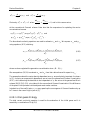
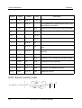
MESH:NX=35,NY=35,XX=2,YY=2.5,IM=1, COMM=’Deposition example’;
SUBS:PH=1E12,BO=1E13,AS=1E12,OR=111;
BODE:XD=3 CS=1.E18;
ANNE:TC=1000,TM=1800,TA=200 OX=0;}
ASDE:XD=1 CS=1E20;
ANNE:TC=1100,TM=1800,TA=100 OX=0;$
4.9.5. Buried layer and epitaxy
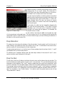
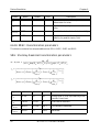
A substrate is doped by boron at 1016 cm-3, arsenic is implanted in the whole region at 300 KeV
and 1015 ions/cm2, and annealed at 1000 °C for 1 hour in an inert ambient. Epitaxy follows for 10
minutes at 1200 °C resulting in a layer thickness of 2 microns which is doped by arsenic at 1015
cm-3. Then boron is implanted at 100 KeV and 1012 ions/cm2 into the left side of the region and
annealed at 1000 °C for 60 minutes. A nonuniform mesh is used.
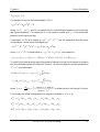
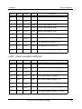
MESH:NX=25,NY=38,XX=2,YY=3.5,IM=0,AX=1.E-5,AY=1,COMM=’Buried layer example’;
SUBS:PH=1E12,BO=1E16,AS=1E12,OR=111;
ASIM:XM=10 EN=300. DZ=1E15;
ANNE:TC=1000,TM=3600,TA=600 OX=0;
EPIT:TH=2 PH=1.E12,BO=1.E12,AS=1.E15 TC=1200,TM=600,TA=150;}
BOIM:XM=1. DZ=1.E12 EN=100;
ANNE:TC=1000,TM=3600,TA=600 OX=0; $
4.9.6. Emitter region
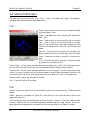
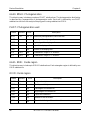
To simulate emitter formation in the large fragment simulated in the previous example only its
small upper region is considered. The substrate is doped by arsenic at 1015 cm-3 with boron
implanted at 100 KeV and 1012 ions/cm2 and arsenic implanted at 60 KeV and 1015 ions/cm2
through the mask into the left half of the region. The wafer is then annealed for 1 hour at 1000 °C.
The mesh is nonuniform in order to resolve a steep initial arsenic profile near the surface.
MESH:NX=15,NY=20,XX=1.,YY=1.1,IM=0 AX=1.E-5 AY=1., COMM=’Emitter region’;
SUBS:PH=1E12,BO=1E12,AS=1E15,OR=111;
BOIM:XM=2 DZ=1.E12 EN=100;
ASIM:XM=0.5 DZ=1.E15 EN=60;
54
MICROTEC-4.0 User’s Manual