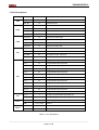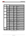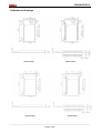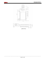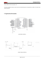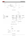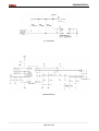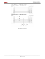
1
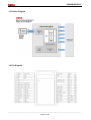
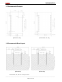
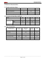
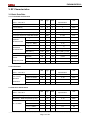
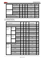
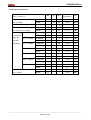
Bluetooth® Class 2 OEM Module Parani-BCD210 Product Datasheet Version 1.0.0 June 18, 2012 Sena Technologies, Inc PARANI-BCD210 Copyright Copyright 2008~2012, Sena Technologies, Inc. All rights reserved. Sena Technologies reserves the right to make changes and improvements to its product without providing notice. Trademark Parani™ is a trademark of Sena Technologies, Inc. Windows® is a registered trademark of Microsoft Corporation. Ethernet® is a registered trademark of XEROX Corporation. Bluetooth® is a registered trademark of Bluetooth SIG (Special Interest Group). Notice to Users When a system failure may cause serious consequences, protecting life and property against such consequences with a backup system or safety device is essential. The user agrees that protection against consequences resulting from system failure is the user's responsibility. This device is not approved for life-support or medical systems. Changes or modifications to this device not explicitly approved by Sena Technologies will void the user's authority to operate this device. Precautions and Safety Do not drop or subject the device to impact. Damage to your products may result from improper use. Keep away from harsh environments including humid, dusty, and smoky areas. Damage to your products may result from improper use. Do not use excessive force on the buttons or attempt to disassemble the device. Damage to your products may result from improper use. Do not place heavy objects on the product. Damage to your products may result from improper use. Contact Information Technical support email: [email protected] Company website: http://www.sena.com ______________________________________________________________________________________ Page 2 of 26 PARANI-BCD210 Contents 1. General .......................................................................................................................................................... 4 1.1 Features ............................................................................................................................................... 4 1.2 Applications .......................................................................................................................................... 4 1.3 Device Diagram .................................................................................................................................... 5 1.4 Pin Diagram.......................................................................................................................................... 5 1.5 Pin Descriptions.................................................................................................................................... 6 1.6 Mechanical Drawings ........................................................................................................................... 8 1.7 Recommended Footprint.................................................................................................................... 10 1.8 Recommended Board Layout............................................................................................................. 10 2. Electrical characteristics ...............................................................................................................................11 2.1 Absolute maximum ratings ..................................................................................................................11 2.2 Recommended operating conditions...................................................................................................11 2.3 Power Consumption ............................................................................................................................11 3. RF Characteristics ....................................................................................................................................... 12 3.1 Basic Data Rate.................................................................................................................................. 12 3.1.1 Transmitter Performance 3.1.2 Transceiver ............................................................................................ 12 ............................................................................................ 12 3.1.3 Receiver Performance ............................................................................................ 12 3.2 Enhanced Data Rate .......................................................................................................................... 13 3.2.1 Transmitter performance 3.2.2 Receiver performance ............................................................................................ 13 ............................................................................................ 14 4. Device Terminal Descriptions ...................................................................................................................... 15 4.1 UART Interface................................................................................................................................... 15 4.2 USB Interface ..................................................................................................................................... 15 2 4.3 I C Interface........................................................................................................................................ 16 4.4 PCM CODEC Interface ...................................................................................................................... 16 4.5 I/O Parallel Ports ................................................................................................................................ 17 4.6 Reset Interface ................................................................................................................................... 17 5. Application Schematic.................................................................................................................................. 18 6. Software Stack............................................................................................................................................. 22 7. Solder Profiles ............................................................................................................................................. 23 8. Packaging Information ................................................................................................................................. 24 9. Certificate Information.................................................................................................................................. 25 9.1 FCC .................................................................................................................................................... 25 9.2 CE....................................................................................................................................................... 26 9.3 IC ........................................................................................................................................................ 26 9.4 KC....................................................................................................................................................... 26 9.5 TELEC ................................................................................................................................................ 26 9.6 SIG ..................................................................................................................................................... 26 ______________________________________________________________________________________ Page 3 of 26 PARANI-BCD210 1. General The Parani-BCD210 is a Bluetooth Class 2 OEM module for OEM manufacturers who want to implement Bluetooth Class 2 functionality with their products cost effectively and also in timely manner. By using ParaniBCD210, users can add low cost Bluetooth functionality to their products easily and quickly while keeping the benefit from the BCD210’s field-proven standard SPP (Serial Port Profile) firmware provided with no additional cost. The BCD210 supports Class 2 Bluetooth transmission level for short communication distance typically ranges from 50 m up to 300m. The BCD210 supports UART, USB, I2C, PCM, PIO interfaces for the communication with the OEM products. The BCD210 is provided with Bluetooth v2.0 compatible firmware runs internally for SPP (Serial Port Profile) applications by default. The SPP firmware supports up to 4 simultaneous multiple connections and is designed to work out-of-box for real world SPP applications such as POS (Point-of-sales), industrial automation, remote metering and other various applications. Optionally, the BCD210 can be supplied with only software stack up to HCI level so entire Bluetooth stack runs on the host side for the application such as USB dongles for computers, or OEM manufacturers can even develop and embed their own firmware into the BCD210. The BCD210 is fully qualified with Bluetooth v.2.0+EDR specification so OEM manufacturers can save cost and time for overall OEM product certifications, which makes the BCD210 ideal solution for larger volume and cost sensitive applications. 1.1 Features - Bluetooth Class 2 (Bluetooth v2.0+EDR) - Transmit Power: +4dBm Typical - Receive sensitivity: -84dBm (0.1% BER) - Integrated 8Mbit Flash Memory - Supports Serial Port Profile (SPP) - Working distance (In an open field): Nom.50m, up to 300m - Supports built-in chip, stub and dipole antennas - Standard HCI over UART or USB - ROHS compliant 1.2 Applications - High-speed Data Transceiver Systems for Short distance communication - PCs/Personal Digital Assistants (PDA) - Bluetooth USB Dongle - Bluetooth Serial Dongle - Bluetooth Access Points - Industrial automation device - Remote metering device - POS (Point-of-sales) devices ______________________________________________________________________________________ Page 4 of 26 PARANI-BCD210 1.3 Device Diagram 1.4 Pin Diagram ______________________________________________________________________________________ Page 5 of 26 PARANI-BCD210 1.5 Pin Descriptions Function Pin Name Pin Number Description USB_DP 11 USB data plus USB_DN 10 USB data minus UART_TXD 8 UART data output UART_RXD 7 UART data input UART_RTS 6 UART request to send active low UART_CTS 9 UART clear to send active low PCM_OUT 15 Synchronous data output PCM_IN 12 Synchronous data input PCM_SYNC 13 Synchronous data sync PCM_CLK 14 Synchronous data clock SPI_MISO 20 SPI data output SPI_MOSI 23 SPI data input SPI_CSB 22 Chip select for SPI, active low SPI_CLK 21 SPI clock PIO_0 35 Programmable input/output line PIO_1 34 Programmable input/output line PIO_2 29 Programmable input/output line PIO_3 28 Programmable input/output line PIO_4 24 Programmable input/output line PIO_5 25 Programmable input/output line PIO_6 26 Programmable input/output line PIO_7 27 Programmable input/output line PIO_8 30 Programmable input/output line PIO_9 31 Programmable input/output line PIO_10 32 Programmable input/output line PIO_11 33 Programmable input/output line AIO_0 4 Analogue programmable input/output line AIO_1 5 Analogue programmable input/output line +3V3 16 Power supply for system, 3.3V GND 1,2,17,19,36 USB UART PCM SPI PIO AIO Power Ground RESETB 18 Reset, active low, > 5ms to cause a reset NC 3 NC Others Table 1-1 Pin descriptions ______________________________________________________________________________________ Page 6 of 26 PARANI-BCD210 STATE Function Pin Name Define (SPP) Direction Pull-up/down USB_DP - Input Weak pull-up USB_DN - Input Weak pull-up UART_TXD UART_TXD Output Tri-stated with weak pull-up UART_RXD UART_RXD Input Weak pull-down UART_RTS UART_RTS Output Tri-stated with weak pull-up UART_CTS UART_CTS Input Weak pull-down PCM_OUT - Output Tri-stated with weak pull-down PCM_IN - Input Weak pull-down PCM_SYNC - Input Weak pull-down PCM_CLK - Input Weak pull-down SPI_MISO - Output Tri-stated with weak pull-down SPI_MOSI - Input Weak pull-down SPI_CSB - Input Weak pull-up SPI_CLK - Input Weak pull-down PIO_0 - Input Weak pull-down PIO_1 - Input Weak pull-down PIO_2 UART_DCD Output Weak pull-down PIO_3 UART_DTR Output Weak pull-down PIO_4 UART_DSR Input Weak pull-up PIO_5 FACTORY_RESET Input Weak pull-up PIO_6 BT_MODE Input Weak pull-up PIO_7 F/C_CTRL Output Weak pull-up PIO_8 - Input Weak pull-down PIO_9 - Input Weak pull-down PIO_10 STATUS_LED0 Output Weak pull-down PIO_11 STATUS_LED1 Output Weak pull-down AIO_0 - Output Driving low AIO_1 - Output Driving low RESETB RESETB Input Weak pull-up USB UART PCM SPI PIO AIO Others Table 1-2 Pin State on Reset ______________________________________________________________________________________ Page 7 of 26 PARANI-BCD210 1.6 Mechanical Drawings [BCD210SU] [BCD210DU] [BCD210SC] [BCD210DC] ______________________________________________________________________________________ Page 8 of 26 PARANI-BCD210 [BCD210DS] ______________________________________________________________________________________ Page 9 of 26 PARANI-BCD210 1.7 Recommended Footprint [BCD210SU, SC] [BCD210DU, DC, DS] 1.8 Recommended Board Layout [BCD210SC] [BCD210DC] *BCD210SU, DU, DS has no keep-out area. ______________________________________________________________________________________ Page 10 of 26 PARANI-BCD210 2. Electrical characteristics 2.1 Absolute maximum ratings Ratings Min Max Unit Storage Temperature -40 +85 °C Operating Temperature -40 +85 °C Supply voltage -0.4 3.6 V GND – 0.4 VCC + 0.4 V Other terminal voltages 2.2 Recommended operating conditions Ratings Min Typ Max Unit Operating Temperature -40 25 +85 °C +3V3 2.7 3.3 3.6 V UART 3.0 3.3 3.6 V USB 3.1 3.3 3.6 V +3V3 60 80 100 mA Supply voltage Supply current 2.3 Power Consumption Connection UART Rate Current Type (Kbps) (Average) Power on (Standby) - 115.2 1.4 mA Inpuiry Scan - 115.2 42 mA Connected (No data) Slave 115.2 21 mA Connected (File transfer) Slave 115.2 29 mA Connected (No data) Master 115.2 5 mA Connected (File transfer) Master 115.2 28 mA Sniff Mode Master 115.2 1.7 mA Operation Mode Unit ______________________________________________________________________________________ Page 11 of 26 PARANI-BCD210 3. RF Characteristics 3.1 Basic Data Rate 3.1.1 Transmitter Performance RF Characteristics Bluetooth Min Typ Max Output power 0 2 4 4 dBm Power Density 0 2 4 4 dBm Power Control 3 4 6 2 ≤ step ≤ 8 dB TX Output Spectrum-Frequency range 2402 - 2480 2400 ~2483.5 MHz TX Output Spectrum-20dB Bandwidth - 900 - ≤ 1000 kHz F = F0 ± 2MHz - - -20 ≤ -20 dBm F = F0 ± 3MHz - - -40 ≤ -40 dBm F = F0 ± > 3MHz - - -40 ≤ -40 dBm Δf1avg 140 165 175 140 ≤ Δf1avg ≤ 175 kHz Δf2avg 115 155 - Δf2avg ≥ 115 kHz Δf2avg/Δf1avg 0.80 0.95 - (Δf1avg/Δf2avg) ≥ 0.8 - -20 - 20 ≤ ±75 kHz Drift rate -20 - 20 ≤ ±20 kHz/50µs 1 slot Freq Drift -25 - 25 ≤ ±25 kHz 5 slot Freq Drift -40 - 40 ≤ ±40 kHz Min Typ Max 0.030-1.000GHz -36 - - ≤ -36 dBm 1.000-12.75GHz -30 - - ≤ -30 dBm 1.800-5.100GHz -47 - - ≤ -47 dBm 5.100-5.300GHz -47 - - ≤ -47 dBm Min Typ Max Sensitivity - Single slot packets (0.1%) - -84 -70 ≤ -70 dBm Sensitivity - Multi slot packets (0.1%) - -84 -70 ≤ -70 dBm VCC = 3.3V, 25°C Adjacent Channel Power Modulation Characteristics Initial Carrier Frequency Tolerance Carrier Frequency Drift Specification Unit 3.1.2 Transceiver RF Characteristics VCC = 3.3V, 25°C Out of band Spurious Emissions Bluetooth Specification Unit 3.1.3 Receiver Performance RF Characteristics VCC = 3.3V, 25°C Bluetooth Specification Unit C/I performance co-channel - - 11 ≤ -11 dB at 0.1% BER F = F0 + 1MHz - - 0 ≤0 kHz F = F0 – 1MHz - - 0 ≤0 dB F = F0 + 2MHz - - -20 ≤ -20 dB ______________________________________________________________________________________ Page 12 of 26 PARANI-BCD210 F = F0 – 2MHz - - -30 ≤ -30 dB F = F0 – 3MHz - - -40 ≤ -40 dB F = F0 + 5MHz - - -40 ≤ -40 dB F = FImage - - -9 ≤ -9 dB Blocking 0.030-2.000GHz -10 - - -10 dBm performance 2.000-2.400GHz -27 - - -27 dBm 2.500-3.000GHz -27 - - -27 dBm 3.000-12.75GHz -10 - - -10 dBm Inter-modulation performance -39 - - ≥ -39 dBm Maximum input level at 0.1% BER -20 - - ≥ -20 dBm 3.2 Enhanced Data Rate 3.2.1 Transmitter performance RF Characteristics Bluetooth Min Typ Max Maximum RF Transmit Power -3 1 - -6 to +4 dB Relative Transmit Power -4 - 1 -4 to +1 dB VCC = 3.3V, 25°C Specification Unit Carrier π/4 | ω0 | -10 - 10 ≤ ±10 for all blocks kHz Frequency DQPSK | ωi | -75 - 75 ≤ ±75 for all packets kHz | ω0 + ωi | -75 - 75 ≤ ±75 for all blocks kHz | ω0 | -10 - 10 ≤ ±10 for all blocks kHz | ωi | -75 - 75 ≤ ±75 for all packets kHz | ω0 + ωi | -75 - 75 ≤ ±75 for all blocks kHz Stability 8DPSK Modulation π/4 RMS DEVM - - 20 ≤ 20 % Accuracy DQPSK 99% DEVM - - 30 ≤ 30 % Peak DEVM - - 35 ≤ 35 % RMS DEVM - - 13 ≤ 13 % 99% DEVM - - 20 ≤ 20 % Peak DEVM - - 25 ≤ 25 % 99 - - ≥ 99 % 8DPSK EDR Differential Phase Encoding In-band F ≥ F0 + 3MHz - - -40 ≥ -40 dBm Spurious F < F0 + 3MHz - - -40 ≥ -40 dBm Emissions F = F0 – 3MHz - - -40 ≥ -40 dBm (8DPSK) F = F0 – 2MHz - - -20 ≥ -20 dBm F = F0 – 1MHz - - -26 ≥ -26 dB F = F0 + 1MHz - - -26 ≥ -26 dB F = F0 + 2MHz - - -20 ≥ -20 dBm F = F0 + 3MHz - - -40 ≥ -40 dBm ______________________________________________________________________________________ Page 13 of 26 PARANI-BCD210 3.2.2 Receiver performance RF Characteristics VCC = 3.3V, 25°C Min Typ Max Bluetooth Specification Unit Sensitivity π/4 DQPSK - -84 -70 ≤ -70 dBm at 0.01% BER 8DPSK - -78 -70 ≤ -70 dBm - - -60 ≤ -60 dBm BER floor performance C/I Performance π/4 DQPSK - - 13 ≤ +13 dB (co-channel at 0.1% BER) 8DPSK - - 21 ≤ +21 dB π/4 DQPSK - - 0 ≤0 dB 8DPSK - - 5 ≤ +5 dB π/4 DQPSK - - 0 ≤0 dB 8DPSK - - 5 ≤ +5 dB π/4 DQPSK - - -30 ≤ -30 dB 8DPSK - - -25 ≤ -25 dB π/4 DQPSK - - -20 ≤ -20 dB 8DPSK - - -13 ≤ -13 dB π/4 DQPSK - - -40 ≤ -40 dB 8DPSK - - -33 ≤ -33 dB π/4 DQPSK - - -40 ≤ -40 dB 8DPSK - - -33 ≤ -33 dB π/4 DQPSK - - -7 ≤ -7 dB 8DPSK - - 0 ≤0 dB C/I F = F0 + 1MHz Performance (Adjacent F = F0 – 1MHz Channel Selectivity) F = F0 + 2MHz F = F0 – 2MHz F ≥ F0 + 3MHz F ≤ F0 – 5MHz F = FImage Maximum input level π/4 DQPSK -20 - - ≥ -20 dBm at 0.1% BER 8DPSK -20 - - ≥ -20 dBm ______________________________________________________________________________________ Page 14 of 26 PARANI-BCD210 4. Device Terminal Descriptions 4.1 UART Interface This is a standard UART interface(TTL-Level) for communicating with other serial devices. BCD210 UART interface provides a simple mechanism for communicating with other serial device using the RS232 protocol. When BCD210 is connected to another digital device, UART_RX and UART_TX transfer data between the two devices. The remaining two signals, UART_CTS, UART_RTS, can be used to implement RS232 hardware flow control where both are active low indicators. All UART connections are implemented using CMOS technology and have signaling levels of 0V and 3.3V Parameter Baud Rate Possible Values Minimum 1200 baud (2%Error) Maximum 4M baud (1%Error) Flow Control RTS/CTS or None Parity None, Odd or Even Number of Stop Bits 1 or 2 Bits per Channel 8 [Possible UART Settings] 4.2 USB Interface BCD210 USB devices contain a full speed (12Mbits/s) USB interface that is capable of driving of a USB cable directly. No external USB transceiver is required. The device operates as a USB peripheral, responding to requests from a master host controller such as a PC. Both the OHCI and the UHCI standards are supported. The set of USB endpoints implemented behave as specified in the USB section of the Bluetooth specification v2.0+EDR or alternatively can appear as a set of endpoints appropriate to USB audio devices such as speakers. As USB is a Master/Slave oriented system (in common with other USB peripherals), BCD210 only supports USB slave operation. ______________________________________________________________________________________ Page 15 of 26 PARANI-BCD210 The USB data lines emerge as pins USB_DP and USB_DN. These terminals are connected to the internal USB I/O buffers of the BCD210, therefore, have low output impedance. To match the connection to the characteristic of the USB cable, resistors must be placed in series with USB_DP/USB_DN and the cable. BCD210 features an internal USB pull-up resistor. This pulls the USB_DP pin weakly high when BCD210 is ready to enumerate. It signals to the PC that it is a full speed (12Mbit/s) USB device. The USB internal pull-up is implemented as a current source, and is compliant with section 7.1.5 of the USB specification v1.2. The internal pull-up pulls USB_DP high to at least 2.8V when loaded with a 15KΩ±5% pull-down resistor (in the hub/host) when VDD_PADS=3.1V. This presents a Thevenin resistance to the host of at least 900Ω. Alternatively, an external 1.5KΩ pull-up resistor can be placed between a PIO line and D+ on the USB cable. The firmware must be alerted to which mode is used by PS key PSKEY_USB_PIO_PULLUP appropriately. The default setting uses the internal pull-up resistor. 4.3 I2C Interface 2 PIO[8:6] can be used to form a mater I C interface. The interface is formed using software to drive these lines. Therefore, it is suited only to relatively slow functions such as driving a dot matrix LCD (Liquid Crystal Display), keyboard scanner or EEPROM. Notes: PIO lines need to be pull-up through 2.2KΩ resistors. PIO[7:6] dual functions, UART bypass and EEPROM support, therefore, devices using an EEPROM cannot support UART bypass mode. 2 For connection to EEPROMs, refer to CSR documentation on I C EEPROM for use with BlueCore. This provides information on the type of devices currently supported. 4.4 PCM CODEC Interface PCM (Pulse Code Modulation) is a standard method used to digitize audio (particularly voice) for transmission over digital communication channels. Through its PCM interface, BCD210 has hardware support for continual transmission and reception of PCM data, thus reducing processor overhead for wireless headset applications. BCD210 offers a bi-directional digital audio interface that route directly into the baseband layer of the on-chip firmware. It does not pass through the HCI protocol layer. Hardware on BCD210 allows the data to be sent to and received from a SCO connection. Up to three SCO connections can be supported by the PCM interface at any on time. BCD210 can operate as PCM interface Master generating an output clock of 128, 256, or 512kHz. When configured as PCM interface slave, it can operate with an input clock up to 2048kHz. BCD210 is compatible with a variety of clock formats, including Long Frame Sync, Short Frame Sync and GCI timing environments. ______________________________________________________________________________________ Page 16 of 26 PARANI-BCD210 It supports 13-bit or 16-bit liner, 8-bit u-law or A-law companied sample formats at 8k samples/s and can receive and transmit on any selection of three of the first four slots following PCM_SYNC. The PCM configuration options are enabled by setting the PS Key PSKEY_PCM_CONFIG32 (0x1b3). BCD210 interfaces directly to PCM audio devices including the following: Qualcomm MSM 3000 series and MSM 5000 series CDMA baseband devices OKI MSM7705 four channel A-raw and u-law CODEC Motorola MC145481 8-bit A-law and u-law CODEC Motorola MC145483 13-bit linear CODEC STW 5093 and 5094 14-bit linear CODECs BCD210 is also compatible with the Motorola SSI TM interface 4.5 I/O Parallel Ports PIO lines can be configured through software to have either weak or strong pull-downs. All PIO lines are configured as inputs with weak pull-downs at reset. Any of the PIO lines can be configured as interrupt request lines or as wake-up lines from sleep modes. PIO_6 or PIO_2 can be configured as a request line for an external clock source. This is useful when the clock to BCD210 is provided from a system ASIC (Application Specific Integrated Circuit). Using PSKEY_CLOCK_REQUEST_ENABLE (0x246), this terminal can be configured to be low when BCD210 is in Deep Sleep and high when a clock is required. The clock must be supplied within 4ms of the rising edge of PIO_6 or PIO_2 to avoid losing timing accuracy in certain Bluetooth operating modes. BCD210 has three general purpose analogue interface pins, AIO_0, AIO_1 and AIO_2. These are used to access internal circuitry and control signals. One pin is allocated to decoupling for the on-chip band gap reference voltage, the other two may be configured to provide additional functionality. 4.6 Reset Interface BCD210 may be reset from several sources: RESETB pin, power on reset, a UART break character or via a software configured watchdog timer. The RESETB pin is an active low reset and is internally filtered using the internal low frequency clock oscillator. A reset will be performed between 1.5 and 4.0ms following RESETB being active. It is recommended that RESETB be applied for a period greater than 5ms. The power on reset occurs when the VDD_CORE supply falls below typically 1.5V and is released when ______________________________________________________________________________________ Page 17 of 26 PARANI-BCD210 VDD_CORE rises above typically 1.6V. At reset the digital I/O pins are set to inputs for bi-directional pins and outputs are tri-state. The PIOs have weak pull-downs. 5. Application Schematic [BT Module Interface] [Power Supply Interface] ______________________________________________________________________________________ Page 18 of 26 PARANI-BCD210 [Reset Interface] [Serial Interface for Host PC] [USB Interface] ______________________________________________________________________________________ Page 19 of 26 PARANI-BCD210 2 [I C Interface] [PCM Interface] ______________________________________________________________________________________ Page 20 of 26 PARANI-BCD210 [MICOM UART Interface] ______________________________________________________________________________________ Page 21 of 26 PARANI-BCD210 6. Software Stack BCD210 is provided with Bluetooth v2.0 compatible firmware runs internally for SPP (Serial Port Profile) applications by default. The firmware is designed to work out-of-box for real world SPP applications such as POS (Point-of-sales), industrial automation, remote metering and other various applications. The SPP firmware can be configured and controlled by typical AT commands. Users can easily configure BCD210 by using a terminal program such as HyperTerminal and can use Bluetooth wireless communication without modifying user’s existing serial communication program. In addition to the basic AT commands, BCD210 provides some expanded AT commands for various functions. User friendly ParaniWizard and ParaniWIN are also provided for easy setup on Microsoft Windows. To run AT commands on the BCD210, the BCD210 should be connected to the serial port of the user’s own board or equivalent to carry the BCD210. The SPP firmware provided with the BCD210 is identical to the firmware of the Parani-ESD100V2 and Parani-ESD110V2. To shorten the overall development cycle or for quick verification during or before own development work, users might want to try ESD100V2/110V2 starter kits first for convenience. Also, please refer to the ESD100V2/110V2 user’s manual for overall concept, configuration and complete AT commands list of the SPP firmware. The ESD100V2/110V2 user’s manual can be downloaded from Sena support home page at http://www.sena.com/support/downloads/. Optionally, the BCD210 can be supplied with only software stack up to HCI level so users can develop and embed their own firmware version into the BCD210 or entire Bluetooth stack runs on the host side for the application such as USB dongle for computers. Regarding these custom firmware options, please contact a Sena representative for more detail. UART SPP Firmware PCM I/O USB UART RFCOMM Host Host L2CAP HCI HCI Link Manager Link Manager Baseband/Link Control Baseband/Link Radio Radio Figure 6-1 SPP Firmware Bluetooth software stack Figure 6-2 HCI firmware Bluetooth Software Stack ______________________________________________________________________________________ Page 22 of 26 PARANI-BCD210 7. Solder Profiles The soldering profile depends on various parameters necessitating a set up for each application. The data here is given only for guidance on solder re-flow. There are four zones: Preheat Zone – This zone raises the temperature at a controlled rate, typically 1-2.5°C/s Equilibrium Zone – This zone brings the board to a uniform temperature and also activates the flux. The duration in this zone (typically 2-3 minutes) will need to be adjusted to optimize the out gassing of the flux. Reflow Zone – The peak temperature should be high enough to achieve good wetting but not so high as to cause component discoloration or damage. Excessive soldering time can lead to intermetal growth which can result in a brittle joint. Cooling Zone – The cooling rate should be fast, to keep the solder grains small which will give a longer lasting joint. Typical rates will be 2-5°C/s [Typical Lead-Free Re-flow Solder Profile] Key features of the profile: Initial Ramp = 1-2.5°C/sec to 175°C±25°C equilibrium Equilibrium time = 60 to 180 seconds Ramp to Maximum temperature (245°C) = 3°C/sec max. Time above liquids temperature (217°C): 45~90 seconds Device absolute maximum reflow temperature: 260°C Devices will withstand the specified profile. Lead-free devices will withstand up to three reflows to a maximum temperature of 260°C ______________________________________________________________________________________ Page 23 of 26 PARANI-BCD210 8. Packaging Information ______________________________________________________________________________________ Page 24 of 26 PARANI-BCD210 9. Certificate Information 9.1 FCC FCC Rule: Part 15 Subpart C Section 15.247 FCCID: S7AIW03 9.1.1 FCC Compliance Statement This device complies with part 15 of the FCC Rules. Operation is subject to the following two conditions: (1) This device may not cause harmful interference, and (2) This device must accept any interference received, Including interference that may cause undesired operation Information to User This equipment has been tested and found to comply with limits for a Class B digital device, Pursuant to Part 15 of the FCC Rules. These limits are designed to provide reasonable protection against harmful interference in a residential installation. This equipment generate, uses and can radiate radio frequency energy and, if not installed and used in accordance with the instructions, may cause harmful interference to radio communications. However, there is no guarantee that interference will not occur in a particular installation. If this equipment does cause harmful interference to radio or television reception, which can be determined by turning the equipment off and on, the user is encouraged to try to correct the interference by on or more of the following measures: - Reorient or relocate the receiving antenna. - Increase the separation between the equipment and receiver-Connect the equipment into an outlet a circuit different form that to which the receiver is connected. - Consult the dealer or an experienced radio/TV technician for help. 9.1.2 RF Exposure Statement The equipment complies with FCC RF radiation exposure limits set forth for an uncontrolled environment. This device and its antenna must not be co-located or operation in conjunction with any other antenna or transmitter. 9.1.3 Do not Any changes or modifications to the equipment not expressly approved by the party responsible for compliance could void user’s authority to operate the equipment. ______________________________________________________________________________________ Page 25 of 26 PARANI-BCD210 9.2 CE Certification No: 1177 Declare under our own responsibility that the product Bluetooth Module Brand name: SENA Model No.: Parani-BCD210DU / Parani-BCD210DC / Parani-BCD210DS Parani-BCD210SU / Parani-BCD210SC To which this declaration refers conforms with the relevant standards or other standardizing documents EN 60950-1 ETSI EN 301 489-1 ETSI EN 301 489-17 ETSI EN 300 328 According to the regulations in Directive 1999/5/EC 9.3 IC Radio Cert. No.: IC: 8154A-IW03 9.4 KC Type Registration Certification No: KCC-CRM-SNA-IW03 9.5 TELEC Technical Regulations for Specified Radio Equipment Article 2, Section 1 (19) Certification No: Parani-BCD210DU: 010WWBT0144 Parani-BCD210DC: 010WWBT0146 Parani-BCD210DS: 010WWBT0145 9.6 SIG QDID: B019536 Model Name: Parani-BCD210 Core Version: 2.0+EDR Product Type: Component Declared Specifications: Baseband Conformance, Radio, Service Discovery Protocol, Logical Link Control and Adaption Protocol, Generic Access Profile, Link Manager, RFCOMM, Serial Port Profile, Host Controller Interface, Summary ICS, Product Type ______________________________________________________________________________________ Page 26 of 26