1
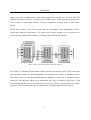
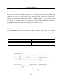
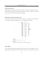
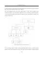
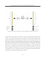
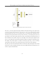
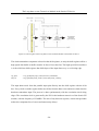
TESLA Report 2006-04
DESY Thesis 2006-000
WARSAW UNIVERSITY OF TECHNOLOGY
Faculty of Electronics and Informational Technologies
Institute of Electronic Systems
ELHEP Laboratory
DESY TESLA LLRF Team
Jerzy Stefan Zieliński
Synchronic, optical transmission data link
integrated with FPGA circuits
(for TESLA LLRF control system)
Mentor:
Prof. D.Sc. Ryszard Romaniuk, WUT
Tutor:
Ph.D. Krzysztof Poźniak, WUT
In cooperation with
Dr Stefan Simrock, DESY, Hamburg
Warsaw, May 2006
Contents
ABSTRACT.................................................................................................................................................................. 4
INTRODUCTION........................................................................................................................................................ 5
The X-FEL Laser Project ..................................................................................................................................... 5
The LLRF system & Stratix GX devices in LLRF Project..................................................................................... 6
INTRODUCTION TO THE STRATIX GX DEVICE.............................................................................................. 8
Overview............................................................................................................................................................... 8
Basic Features ...................................................................................................................................................... 9
Stratix GX Transceivers...................................................................................................................................... 12
Transceiver Blocks ............................................................................................................................................. 12
TRANSMITTER PATH ................................................................................................................................................ 15
Transmitter PLL ................................................................................................................................................. 15
Transmitter Phase Compensation FIFO Buffer.................................................................................................. 16
Byte Serializer .................................................................................................................................................... 16
8B/10B Encoder.................................................................................................................................................. 16
Serializer (Parallel-to-Serial Converter)............................................................................................................ 17
Transmit Buffer................................................................................................................................................... 18
Programmable Output Driver ............................................................................................................................ 18
Programmable Transmitter Termination............................................................................................................ 19
RECEIVER PATH ....................................................................................................................................................... 19
Receiver Input Buffer.......................................................................................................................................... 19
Receiver PLL & CRU ......................................................................................................................................... 20
Deserializer (Serial-to-Parallel Converter) ....................................................................................................... 20
Word Aligner ...................................................................................................................................................... 20
8B/10B Decoder ................................................................................................................................................. 22
Applications & Protocols ................................................................................................................................... 23
THE LONG-DATA-VECTORS TRANSCEIVER MODULE IN THE STRATIX GX DEVICE...................... 24
Introduction ........................................................................................................................................................ 24
The Long-Data-Vector serializer........................................................................................................................ 26
The hardware transceiver module in the Stratix GX FPGA structure................................................................ 30
The long data vector deserializer ....................................................................................................................... 32
TESTS OF THE LONG-DATA-VECTOR TRANSCEIVER MODULE ............................................................. 35
SIMULATIONS IN THE QUARTUS II SOFTWARE .......................................................................................................... 35
HARDWARE RANDOM TESTS ..................................................................................................................................... 36
-2-
SUMMARY ................................................................................................................................................................ 38
LITERATURE ........................................................................................................................................................... 41
ACKNOWLEDGMENT
We acknowledge the support of the European Community Research Infrastructure Activity under the FP6
“Structuring the European Research Area” program (CARE, contract number RII3-CT-2003-506395).
-3-
Abstract
The X-ray free-electron laser X-FEL that is being planned at the DESY research center in
cooperation with European partners will produce high-intensity ultra-short X-ray flashes with the
properties of laser light. This new light source, which can only be described in terms of
superlatives, will open up a whole range of new possibilities for the natural sciences. It could also
offer very promising opportunities for industrial users.
SIMCON (SIMulator and CONtroller) is the project of the fast, low latency digital controller
dedicated to the LLRF1 system in VUV FEL experiment It is being developed by the ELHEP2
group in the Institute of Electronic Systems at Warsaw University of Technology. The main
purpose of the project is to create a controller to stabilize the vector sum of fields in cavities of
one cryo-module in the experiment. The device can be also used as the simulator of the cavity
and test bench for other devices.
The synchronic, optical link project was made for the accelerator X-FEL laser TESLA, the LLRF
control system experiment at DESY, Hamburg. The control and diagnostic data is transmitted up
to 2.5Gbit/s through a plastic fiber in a distance up to a few hundred meters. The link is
synchronized once after power up, and never resynchronized when data is transmitted with
maximum speed. The one way link bit error rate is less then 10-15. The transceiver component
written in VHDL that works in the dedicated Altera® Stratix® GX FPGA circuit. During the
work in the PERG laboratory a 2,5Gbit/s serial link with the long vector parallel interface
transceiver was created. Long-Data-Vector transceiver transmits 16bit vector each 8ns with
120ns latency.
1
Low level Radio Frequency
2
Electronics for High Energy Physics
-4-
Introduction
Introduction
The X-FEL Laser Project
The X-ray free-electron laser XFEL will produce high-intensity ultra-short X-ray flashes with the
properties of laser light. The experiment that is being planned at the DESY research center in
cooperation with European partners introduces a new light source, that can only be described in
terms of superlatives. The X-FEL laser will open up a whole range of new possibilities for the
natural sciences. The overall layout of the X FEL linear accelerator and laser facility is shown in
Figure 1.
Figure 1 X-FEL facility layout
-5-
Introduction
The main X FEL parameters are:
•
Total length of the facility: approx. 3.4 km
•
Accelerator tunnel: approx. 2.1 km
•
Depth underground: 6 - 38 m
•
Wavelength of X-ray radiation: 6 to 0.085 nanometers (nm) corresponding to electron
energies of 10 to 20 billion electron volts (GeV)
•
Length of radiation pulses: below 100 femtoseconds (fs)
The planned facility will include a superconducting linear accelerator, and a full control system
with measurement capabilities. The accelerator brings tightly bundled "bunches" of electrons to
energies of several billion electron volts. As electrons go through the accelerator cavities, they
emit X-ray radiation that amplifies itself during the flight. In result extremely short and intense
X-ray flashes with laser properties appears. The X-ray laser requires extremely high quality of an
electron beam. The TESLA superconducting accelerator technology makes it possible to generate
precise beam of electrons.
The cavities of the accelerator are grouped in cryomodules.(Figure 2) Each cryomodule consists
of 32 cavities. In general, four cryomodules are driven by one klystron. In order to accelerate the
beam, the electromagnetic field inside the cavity must be stabilized. The regulation of the field is
performed by the LLRF system The system controls I and Q components of the cavity field
(which corresponds to real and imaginary part of the field vector).
Figure 2 The layout of accelerator module construction
The LLRF system & Stratix GX devices in LLRF Project
The LLRF control system is responsible for a precise repetitive loading of the cavity with the EM
high power energy field and for the EM field stabilization. A single channel system works with a
-6-
Introduction
single cavity. The 8 channel system works with a single TESLA module (ACC) of 8 cavities. The
modular electronic work up to 32 cavities per an LLRF system. In the future the system will be
able to control a much larger number of system components referring to the X-FEL system
project.
In the above context, The LLRF system may be represented as the multichannel, sourcesynchronous hardware concentrator. The signals from various number of A/D converters are
delivered to the concentration module via elemental signal boards and elements.
Figure 3 LLRF system components connections diagram
The LLRF is a distributed, multichannel control and data transmission system. The control and
data acquisition boards are connected together with fast data links. (Figure 3) Standard wires or
fiber cables can be used for data transmission there. Standard Cu wires may be influenced by the
strong EM field and data, which travels through the wire can be scrambled. Optic fiber is EM
field resistant and data can not be scattered in an easy way. Fiber is a perfect choice for boards
connection. The fast optical link can be established at 2,5 Gbps using Stratix GX Devices.
-7-
The Stratix GX Device
Introduction to the Stratix GX Device
Expansion in the telecommunications market and growth in Internet use requires systems to move
more data faster than ever. To meet this demand, system designers rely on solutions such as
differential signaling and emerging high-speed interface standards including RapidIO, POS-PHY
4, SFI-4, or XSBI. These new protocols support differential data rates up to 1 gigabit per second
(Gbps) and higher. At these high data rates, it becomes more challenging to manage the skew
between the clock and data signals. One solution to this challenge is to use clock data recovery
(CDR) to eliminate skew between data channels and clock signals. Another potential solution,
dynamic phase alignment (DPA), is beginning to be incorporated by some of these protocols. The
Stratix™ GX family of devices are the first FPGA devices to have an embedded dynamic phase
aligner.
Overview
The Stratix® GX family combines high-speed serial transceivers with a scalable, highperformance logic array. Stratix GX devices include 4 to 20 high-speed transceiver channels,
each incorporating a clock data recovery (CDR) technology and embedded serializer-deserializer
(SERDES) capability at data flow rates of up to 3.1875Gbit/s. Transceivers are grouped by fourchannel transceiver blocks. The Stratix GX FPGA technology offers scalable, high-performance
architecture, witch makes Stratix GX devices ideal for high-speed backplane interface, chip-tochip, and communications protocol-bridging applications.
-8-
The Stratix GX Device
Basic Features
Transceiver block features are as follows:
•
High-speed serial transceiver channels with CDR3 provides 500-megabits per second
(Mbps) to 3.1875-Gbps full-duplex operation
•
Devices are available with 4, 8, 16, or 20 high-speed serial transceiver channels providing
up to 127.5 Gbps of full-duplex serial bandwidth
•
Support for transceiver-based protocols, including 10 Gigabit Ethernet attachment unit
interface (XAUI), Gigabit Ethernet (GigE), and SONET/SDH
•
Compatible with PCI Express, SMPTE 292M, Fibre Channel, and Serial RapidIO I/O
standards
•
Programmable differential output voltage (VOD), pre-emphasis, and equalization settings
for improved signal integrity
•
Individual transmitter and receiver channel power-down capability implemented
automatically by the Quartus® II software for reduced power consumption during nonoperation
•
Programmable transceiver-to-FPGA interface with support for 8-, 10-, 16-, and 20-bit
wide data paths
•
1.5-V pseudo current mode logic (PCML) for 500 Mbps to 3.1875 Gbps
•
Support for LVDS, LVPECL, and 3.3-V PCML on reference clocks and receiver input
pins (AC-coupled)
3
•
Built-in self test (BIST)
•
Hot insertion/removal protection circuitry Stratix GX Transceivers
•
Pattern detector and word aligner supports programmable patterns
Clock Data Recovery
-9-
The Stratix GX Device
•
8B/10B encoder/decoder performs 8- to 10-bit encoding and 10-to 8-bit decoding
•
Rate matcher compliant with IEEE 802.3-2002 for GigE mode and with IEEE 802-3ae for
XAUI mode
•
Channel bonding compliant with IEEE 802.3ae (for XAUI mode only)
•
Device can bypass some transceiver block features if necessary
FPGA features are as follows:
•
10,570 to 41,250 logic elements (LEs)
•
Up to 3,423,744 RAM bits (427,968 bytes) available without reducing logic resources
•
TriMatrix™ memory consisting of three RAM block sizes to implement true dual-port
memory and first-in-out (FIFO) buffers
•
Up to 16 global clock networks with up to 22 regional clock networks per device region
•
High-speed DSP blocks provide dedicated implementation of multipliers (faster than 300
MHz), multiply-accumulate functions, and finite impulse response (FIR) filters
•
Up to eight general usage phase-locked loops (four enhanced PLLs and four fast PLLs)
per device provide spread spectrum, programmable bandwidth, clock switchover, realtime PLL reconfiguration, and advanced multiplication and phase shifting
•
Support for numerous single-ended and differential I/O standards
•
High-speed source-synchronous differential I/O support on up to 45 channels for 1-Gbps
performance
•
Support for source-synchronous bus standards, including 10-Gigabit Ethernet XSBI,
Parallel RapidIO, UTOPIA IV, Network Packet Streaming Interface (NPSI),
HyperTransportTM technology, SPI-4 Phase 2 (POS-PHY Level 4), and SFI-4
•
Support for high-speed external memory, including zero bus turnaround (ZBT) SRAM,
quad data rate (QDR and QDRII) SRAM, double data rate (DDR) SDRAM, DDR fast
cycle RAM (FCRAM), and single data rate (SDR) SDRAM
- 10 -
The Stratix GX Device
•
Support for multiple intellectual property megafunctions from Altera® MegaCore®
functions and Altera Megafunction Partners Program (AMPPSM) megafunctions Support
for remote configuration updates
•
Dynamic phase alignment on LVDS receiver channels
The features of different models of the Stratix GX devices are presented in the Table 1:
Feature
EP1SGX10C
EP1SGX10D
LEs
Transceiver channels
Source-synchronous channels
M512 RAM blocks (32 × 18 bits)
M4K RAM blocks (128 × 36 bits)
M-RAM blocks (4K ×144 bits)
Total RAM bits
Digital signal processing (DSP) blocks
Embedded multipliers
PLLs
10,570
4, 8
22
94
60
1
920,448
6
48
4
EP1SGX25C
EP1SGX25D
EP1SGX25F
25,660
4, 8, 16
39
224
138
2
1,944,576
10
80
4
EP1SGX40D
EP1SGX40G
41,250
8, 20
45
384
183
4
3,423,744
14
112
8
Table 1 Featires of the Stratix GX devices
The Stratix GX device family supports high-speed serial transceiver blocks. Channels are
clustered in a four-channel serial transceiver building blocks and deliver high-speed bidirectional
point-to-point data transmissions to provide fast, full-duplex data transmission.
The Stratix GX devices supports such source-synchronous, transmission protocols as: LVDS,
LVPECL, 3.3-V PCML, or HyperTransport technology I/O standards.
- 11 -
The Stratix GX Device
Stratix GX Transceivers
Stratix® GX devices incorporate dedicated embedded circuitry on the right side of the device,
which contains up to 20 high-speed 3.1875Gbit/s serial transceiver channels. Each Stratix GX
transceiver block contains four full-duplex channels and supporting logic to transmit and receive
high-speed serial data streams. The transceiver block uses the channels to deliver bidirectional
point-to-point data transmissions with up to 3.1875Gbit/s of data transition per channel.
Transceiver Blocks
Stratix GX devices are organized into four-channel blocks with four full-duplex channels per
block. (Figure 4) Each self-contained Stratix GX gigabit transceiver block supports a variety of
embedded functions:
•
Supports frequencies up to 3.1875Gbit/s
•
Integrates serializer/deserializer (SERDES), clock data recovery (CDR), word aligner,
channel aligner, rate matcher, 8B/10B encoder/decoder, byte serializer/deserializer, and
phase compensation first-in first-out (FIFO) modules
•
Supports flexible reference clock generation capabilities, including a dedicated transmitter
phase-locked loop (PLL) and four receiver PLLs per gigabit transceiver block
•
Includes built-in self test (BIST) capability, including embedded Pseudo Random Binary
Sequence (PRBS) pattern generation and verification
- 12 -
The Stratix GX Device
Figure 4 Starix GX Transceiver Block Diagram
- 13 -
The Stratix GX Device
Each Stratix GX transceiver channel consists of a transmitter and receiver.
The transmitter contains:
•
Transmitter PLL
•
Transmitter phase compensation FIFO buffer
•
Byte serializer
•
8B/10B encoder
•
Serializer (parallel to serial converter)
•
Transmitter output buffer
The receiver contains:
•
Input buffer
•
Clock recovery unit (CRU)
•
Deserializer
•
Pattern detector and word aligner
•
Rate matcher and channel aligner
•
8B/10B decoder
•
Receiver logic array interface
The Stratix GX transceiver functions are set through the Quartus II software, where
programmable pre-emphasis, programmable equalizer, programmable VOD, and the other
transceiver components can be dynamically set. Each Stratix GX transceiver channel is capable
of BIST4 generation and verification in addition to various loopback modes.
4
Build In Self Test
- 14 -
The Stratix GX Device
Stratix GX transceivers provide physical coding sublayer (PCS) and physical media attachment
(PMA) implementation for protocols such as: 10-gigabit XAUI and GigE. The PCS portion of the
transceiver consists of the logic array interface, 8B/10B encoder/decoder, pattern detector, word
aligner, rate matcher, channel aligner, and the BIST and pseudo-random binary sequence pattern
generator/verifier. The PMA portion of the transceiver consists of the serializer/deserializer, the
CRU, and the I/O buffers.
Transmitter Path
This section describes the data path through the Stratix GX transmitter.
Path of Data in Stratix GX transmitter is as follows:
•
Transmitter PLL5
•
Transmitter phase compensation FIFO6 buffer
•
Byte serializer
•
8B/10B encoder
•
Serializer (parallel to serial converter)
•
Transmitter output buffer
Transmitter PLL
The inclk clock is the input into the transmitter PLL. There is one inclk clock per transceiver
block. This clock can be fed by either the refclkb pin, PLD routing, or the inter-transceiver
routing line. The transmitter PLL in each transceiver block clocks the circuits in the transmit
path. The transmitter PLL is also used to train the receiver PLL. If no transmit channels are used
5
6
Phase Locked Loop
First In First Out
- 15 -
The Stratix GX Device
in the transceiver block, the transmitter PLL can be turned off. The transmitter PLL has a
programmable loop bandwidth that can be set to low or high. The loop bandwidth parameter can
be statically set in the Quartus II software.
Transmitter Phase Compensation FIFO Buffer
The transmitter phase compensation FIFO buffer resides in the transceiver block at the PLD
boundary. This FIFO buffer compensates for the phase differences between the transmitter
reference clock (inclk) and the PLD interface clock (tx_coreclk). The phase difference between
the two clocks must be less than 360°. The PLD interface clock must also be frequency locked to
the transmitter reference clock. The phase compensation FIFO buffer is four words deep and
cannot be bypassed.
Byte Serializer
The byte serializer takes double-width words (16 or 20 bits) from the PLD interface and converts
them to a single width word (8 or 10 bits) for use in the transceiver. The transmit data path after
the byte serializer is single width (8 or 10 bits). The byte serializer is bypassed when single width
mode (8 or 10 bits) is used at the PLD interface.
8B/10B Encoder
The 8B/10B encoder translates 8-bit wide data, described as the data string or the control string
by control enable bit into a 10-bit encoded data. The 8B/10B encoder can be bypassed. Figure
diagrams the encoding process.
- 16 -
The Stratix GX Device
Figure 5 The 8b/10b coding diagram
Serializer (Parallel-to-Serial Converter)
The serializer converts the parallel 8-bit or 10-bit data into a serial stream, transmitting the LSB
first. The serialized stream is then fed to the transmit buffer. Figure is a diagram of the serializer.
Figure 6 Parallel-to-Serial Converter Shift Register diagram
- 17 -
The Stratix GX Device
Transmit Buffer
The Stratix GX transceiver buffers support the 1.5-V pseudo current mode logic (PCML) I/O
standard at a rate up to 3.1875 Gbps, across up to 40 inches of FR4 trace, and across 2
connectors. Additional I/O standards, LVDS, 3.3-V PCML, LVPECL, can be supported when
AC coupled. The common mode of the output driver is 750 mV. The output buffer, consists of a
programmable output driver and a programmable pre-emphasis circuit.
Programmable Output Driver
The programmable output driver can be set to drive out 400 to 1,600 mV. Table shows the
available settings for each termination value. The VOD can be dynamically or statically set. The
output driver requires either internal or external termination at the source.
Termination Setting
100
120
150
VOD Setting (mV)
400, 800, 1000, 1200, 1400, 1600
480, 960, 1200, 1440
600, 1200, 1500
Table 2 Voltage Output Driver settings in the Stratix GX devices
- 18 -
The Stratix GX Device
Figure 7 Single-Ended and Differential Waveforms of Programmable Output Driver
Programmable Transmitter Termination
The programmable termination can be statically set in the Quartus II software. The values are
100Ω, 120Ω, 150Ω, and off.
Receiver Path
This section describes the data path through the Stratix GX receiver.
Data travels through the Stratix GX receiver via the following modules:
•
Receiver Input Buffer
•
Clock Recovery Unit (CRU)
•
Deserializer
•
Pattern detector and word aligner
•
Rate matcher and channel aligner
•
8B/10B decoder
•
Receiver logic array interface
Receiver Input Buffer
The Stratix GX receiver input buffer supports the 1.5-V PCML I/O standard at a rate up to 3.1875
Gbps.. The common mode of the input buffer is 1.1 V. The receiver can support Stratix GX-toStratix GX DC coupling.
- 19 -
The Stratix GX Device
Receiver PLL & CRU
Each transceiver block has four receiver PLLs and CRUs, each of which is dedicated to a receive
channel. If the receive channel associated with a particular receiver PLL or CRU is not used, then
the receiver PLL or CRU is powered down for the channel.
Deserializer (Serial-to-Parallel Converter)
The deserializer converts the serial stream into a parallel 8- or 10-bit data bus. The deserializer
receives the least significant bit first. Figure 2–14 is a diagram of the deserializer.
Figure 8 Serail-to-Parallel Converter Shift Register Diagram
Word Aligner
The word aligner aligns the incoming data based on the specific byte boundaries. The word
aligner has three customizable modes of operation: bit-slip mode, 16-bit mode, and 10-bit mode,
- 20 -
The Stratix GX Device
the last of which is available for the basic and SONET modes. There are several ways to align the
data. Word Aligner patterns are shown on the Figure 9.
The 10-bit alignment mode with 8b/10b coding module is used in the Long-Data-Vector
Transceiver Module. The auto-dynamic alignment process is achieved with the Long-DataVector serialization module, that controls the internal I/O pins of the hardware module of the
Stratix GX transceiver.
Figure 9 Word Aligner modes in Stratix GX device
The word aligner module contains a fully programmable pattern detector to identify specific
patterns within the incoming data stream. The pattern detector includes recognition support
- 21 -
The Stratix GX Device
/K28.5/ comma characters for 8B/10B encoded data and A1 or A2 frame alignment patterns for
scrambled signals. Additionally, you can specify a custom alignment pattern in lieu of the /K28.5/
comma. The word aligner in the gigabit transceiver block also creates words from the incoming
serial data stream by realigning the data based on identified byte boundaries. The realignment
function uses a barrel shifter and works with the pattern detector. Additionally, the word aligner
has a manual data realignment mode that lets you control the data realignment in user mode
without consistent alignment characters.
8B/10B Decoder
The 8B/10B decoder converts the 10-bit encoded code group into 8-bit data and 1 control bit. The
8B/10B decoder can be bypassed. The following is a diagram of the conversion from a 10-bit
encoded code group into 8-bit data and 1-bit control.
Figure 10 The 8b/10b decoding process diagram
The 8B/10B encoding/decoding is the backbone of many transceiver protocols, and it is often
used in proprietary implementations. The gigabit transceiver block has dedicated circuitry to
perform 8B/10B encoding in the transmitter and decoding in the receiver. This coding technique
ensures sufficient data transitions and a DC balanced stream in the data signal for successful data
recovery at the receiver.
- 22 -
The Stratix GX Device
Applications & Protocols
Designers can use Stratix GX multi-gigabit transceiver blocks for a wide variety of applications.
The multi-gigabit transceiver block works with a variety of industry-standard protocols, and
supports proprietary custom implementations. The source-synchronous high-speed interface in
Stratix GX devices is a dedicated circuit embedded into the programmable logic device (PLD)
allowing for high-speed communications.
Bus Transfer Protocol
SONET backplane
10 Gigabit Ethernet XAUI
10 Gigabit fibre channel
InfiniBand
Fibre channel (1G, 2G)
Serial RapidIO
PCI Express
SMPTE 292M
Stratix GX (Gbps)
(Supports up to 3.1875 Gbps)
2.488
3.125
3.1875
2.5
1.0625; 2.125
1.25; 2.5; 3.125
2.5
1.485
Table 3 Available transmission protocols in the Stratix GX device
- 23 -
The Long-data-vectors Transceiver Module in the Stratix GX device
The Long-data-vectors Transceiver Module in the Stratix GX device
Introduction
The long data vectors transceiver module is a source-synchronous high-speed interface, working
at 2.5 Gbps. It is implemented in Stratix GX, one of the Altera FPGA family davices. The long
data vectors transceiver component is described in the VHDL language, and uses internal
hardware modules of Stratix® GX device in the process of data transmission. Hardware devices,
dedicated to telecommunication purposes, can transmit data up to 3.125 Gbps with no
resynchronization delays.
The main goals of 2.5Gbit/s transceiver module are:
•
source synchronous work
•
one synchronization
•
bit error rate less then 10-12
•
minimum I/O’s
•
full component control with I/O’s
The FPGA based transceiver module is dedicated to transmission and reception of long bit
vectors through a fiber at 2.5 Gbps. The transceiver consists of two parts: a long-vectortransmitter and a long-vector-receiver, combined in one module, but used separately. The long
vector transceiver path is shown in Figure 11.
- 24 -
The Long-data-vectors Transceiver Module in the Stratix GX device
Figure 11 Schematic of the Long-Data-Vectors Transceiver Module in the Altera Stratix GX device
A long bit data vector is put by a user in the data_in input of the component and confirmed with
the data_in_valid signal. The serialization of data is done in two modules: the 8-bit-serializationmodule and the hardware transmitter (Figure 12) which is a part of the Stratix® GX device. The
FPGA chip is connected to the fiber transmitter module, where electric LVDS impulses are
converted into the electric current that drives the laser led. Data travels through the fiber with the
full speed of 2.5 Gbps and later received by the PIN diode fiber-receiver, which is connected to
FPGA device via symmetric line in LVDS logic. The multi-gigabit voltage pulses drive the
hardware components of the Stratix GX receiver module. Data recovered from the voltage stream
is deserialized in the receiver module of the Stratix GX chip and the 8-bit-deseraliztion-module.
The long-data-vector transmission path is shown in Figure 12.
- 25 -
The Long-data-vectors Transceiver Module in the Stratix GX device
Figure 12 The long-data-vector transmission path in the designed hardware
The Long-Data-Vector serializer
The long-data-vector serializer is the first part of the transmitter module implemented in the
FPGA Stratix GX structure. The synchronic 8-bit serializer module accepts a user data vector
when user data_in_data_valid signal is high, and coreclk7 reference clock signal goes high. The
long data vector is serialized by 8 bits, and synchronously transferred to the hardware transmitter
input (Figure 13)
7
Correlation Clock signal in Stratix GX hardware transceiver module
- 26 -
The Long-data-vectors Transceiver Module in the Stratix GX device
Figure 13 Long-Data-Serializer interfave in Stratix GX device
The data_in_valid user signal is the logical validator of the input data long vector. Input vectors
are always accepted when the last byte of the pervious vector is sent, in this particular moment
the busy indicator goes down. If a user sends the data_in_valid signal while component is busy,
all the data will be ignored and not send by the link. The data_in_valid signal given by the user
goes directly to the control register. that drives all the events during the synchronous process of
data serialization in the module. (Figure 14) The length of the control register depends on the
data_in vector length and is generated automatically during the component compilation process.
The length of the control register is a number of 8-bit bytes in the data_in vector. The binary
representation of the control vector controls the the state of the I/O bits of the component.
The other part of the 8-bit-serialization module is the data flow path, that depends on the control
buffer state. In order to minimize the latency and errors in high speed data rewriting process, it is
made as a separate functional block.
- 27 -
The Long-data-vectors Transceiver Module in the Stratix GX device
Figure 14 Control signals in the Long-Data-Vector Serializer Module in the Stratix GX divice
The whole transmitter component is based on the shift registers, as only the shift registers offers a
high speed data buffer-to-buffer transfer in time of less then 2ns. The high speed 8-bit-serializer
is in fact 8-bit-bus-shift-register, that shifts bytes of the input data every coreclk rising edge.
reg_signal
<= reg_signal((data_length_mod8-9) downto 0) & "00000000";
data_out
<=reg_signal((data_length_mod8-1) downto (data_length_mod8-8));;
The input data travels from the parallel input pins directly into the shift register with the 8-bit
bus. Every clock event the register shifts next 8-bits from the data vector and moves them into the
hardware transmitter input. The process is done synchronously with the correlation clock rising
edges. The correlation clock is generated by the PLL in the hardware tranceiver of the Stratix GX
module, with the frequency of 250MHz. The lack of any between registers, or data storage lathes
makes the component free of errors and unnecessary delays.
- 28 -
The Long-data-vectors Transceiver Module in the Stratix GX device
Figure 15 The data serialization process in the Long-Data-Vector serialization module
The shift register 8-bit-serializer-block construction is free of errors and unnecessary delays. The
component inside buffers are such that they enable an easy reconfiguration of the Long-DataVector sraialization module to allow it to accept data length staring from 8 bits.
entity mux_2500 is
generic
(
data_length
);
port
(
reset
clk
data_in_valid
data_in
data_out
data_out_valid
busy
);
end entity;
:
integer
:
:
:
:
:
:
:
in
in
in
in
out
out
out
std_logic;
std_logic;
std_logic;
std_logic_vector ((data_length-1) downto 0);
std_logic_vector (7 downto 0);
std_logic;
std_logic
The Long-Data-Vector serialization module is realized in the VHDL language, and it can be
implemented in the Stratix GX devices. The high stability and the data reliability makes the
vector serializer ideal for the multigigabit data transmissin link purposes, Component also
controls the hardware transceiver module I/O pins.
- 29 -
The Long-data-vectors Transceiver Module in the Stratix GX device
The hardware transceiver module in the Stratix GX FPGA structure
The fast, source-synchronous data transmission at 2.5 Gbps is possible because of the hardware
elements in the FPGA structure. The hardware elements combined together make the transceiver
module that contains of two major pars: the transmitter and the receiver. The transmitter part is
dedicated to the data coding and serialization process. In the process there is used 8b/10b coding
method that improves the stability, and reliability if the data flow. The coding, designed by the
IBM corporation that is used in serial data transfer protocols, converts 8-bit data vectors in to 10bit vectors, with the same number of ‘0’ and ‘1’ in the stream. In this process the summary
energy of 0’s and 1’s transmitted through the link is close to zero. Data conversion process is
usually used in the symmetric line transmission, and fiber connections. Both of these connections
are used in the project, parallel line to connect FPGA with the fiber transceiver and the optical
connection between the fiber transmitter and receiver. The Stratix GX contains of hardware
transceiver module which is directly connected to the fiber transceiver module. The hardware
transceiver module in FPGA structure is made of hardware blocks connected to user I/O’s.
(Figure 16) With the hardware transceiver I/O pins the full component control is possible.
Figure 16 Hardware transceiver module in the Stratix GX device
- 30 -
The Long-data-vectors Transceiver Module in the Stratix GX device
signal
inclk[]
rx_enacdet[]
rx_in[]
rx_slpbk[]
length
1
1
1
1
tx_in[]
tx_ctrlenable[]
8
1
rx_disperr[]
1
rx_patterndetect[]
1
rx_ctrldetect[]
tx_out[]
rx_errdetect[]
rx_out[]
coreclk_out[]
1
1
1
8
1
rx_clkout[]
rx_syncstatus[]
1
1
description
Transceiver block transmitter PLL reference input clock
Enables alignment to the programmed pattern.
Transceiver block receiver channel data input port.
Reverse serial loopback input. Dynamically enables reverse
serial loopback from the rx_in[] port to the tx_out[] port
Transceiver block transmitter channel data input port.
Control character enable. Enables the 8B/10B encoder to
identify control characters. Labels an input character as a
control code
Indicates whether the 8B/10B decoder detects a disparity
error.
Indicates whether the pattern detector detected the
programmed pattern.
Indicates whether the 8B/10B decoder detects a control code.
Serialized transceiver block transmitter channel data signal.
Indicates whether the 8B/10B decoder detects an error code.
Transceiver block receiver PLL output data.
Output clock fed by the clk2 port of the transceiver block
transmitter PLL.
Output clock from the transceiver block receiver channel.
Provides the status of the pattern detector and word aligner.
- 31 -
The Long-data-vectors Transceiver Module in the Stratix GX device
The long data vector deserializer
The long data vector deserializer module is the last part of the Long-Vector-Transceiver
Component implemented in the FPGA Stratix GX structure. The fast, synchronous module
accepts 8-bit data form the receiver part of the hardware Stratix GX transceiver module, and
transforms them into the long data vector, corresponding with the input data vector. (Figure 17)
Figure 17 Data flow in the Long-Data-Vector Deserializer module in the Strztix GX structure
The vector-deserializer module accepts the 8-bit data vectors from the receiver part of the
hardware Stratix GX module. The incoming data is validated by the rx_control_detect signal, that
is the internal signal of the hardware transceiver module. The signal indicates if the incoming
data is control or data vector. If the control string is detected then component switches into
synchronization mode. If the data vectors are detected then the desalinization process occurs.
- 32 -
The Long-data-vectors Transceiver Module in the Stratix GX device
Figure 18 Control signals in the Long-Data-Vector deserializetion module in the Stratix GX device
The deserialization process is dependent of the state of the control register. (Figure 18) The
control register sets all the I/O’s of the deserialization module. The register also controls the
synchronization signals of the hardware transceiver module.
The second part of the deserialization module is a data flow part. The incoming data is latched in
the internal shift buffer, that is responsible of the byte deserialization. Only the shift buffer
construction make it possible to transmit the data through the registers at speed of 250MHz.
Every clock event the 8-bit data in the register is shifted and transferred on the output pins of the
component. If the data vector is the same as the input vector, the data_out_valid signal rises for
the time of the one clock period. In order to receive the data vector for the output pins of the
component a user must to latch the output data in the outside buffer.
- 33 -
The Long-data-vectors Transceiver Module in the Stratix GX device
Figure 19 The deserialization process in the Data-Vector Deserialization module
The shift register in the deserialization module works in the synchronous mode. The
synchronization signal is given by the hardware transceiver module. Hardware transceiver
module depends of the Deserialization Module signals. The length of the control signals depend
of the number of 8 bit words in the stream. 8 bit words in the data stream in right order make the
output long data vector. The vector is given to a user with the data_out_valid signal, that
corresponding with the valid data in the output.
- 34 -
Tests of the Long-Data-Vector Transceiver Module
Tests of the Long-Data-Vector Transceiver Module
This section tells about the tests of the Long-Data-Vector Transceiver Module. The tests ware
done in the PERG laboratory, and ware using all the available hardware equipment, that was
necessary to fully test the component.
Simulations in the Quartus II software
The 32-Long-Data-Vector Transceiver Module was implemented to the Quartus II 5.0 software
environment.
The 32-Long-Data Vector was incremented by 2 every corelation clock rising edge. All the
transmission signals ware outputed into the chart, and tested toggether, during the simulation at
full transmission speed. This test shows the synchronization process and begin of normal
transmission, referring to Figure 20.
Figure 20 Data transmission simulation in Quartus II software environment
The figure shows the process of synchronization, sending the BC data, and the folowing bytes of
the transmission data stream.
- 35 -
Tests of the Long-Data-Vector Transceiver Module
Hardware random tests
This section tells about hardware tests using the pseudo-random techniques. Long term hardware
tests ware necessary to test the work of the component.
Hardware test was using the Internal Interface and PC Matlab environment. The graphical user
interface was created to make the test users friendly (Figure 21).
Figure 21 GUI for the hardware random test using the Long-Data-Vector Transceiver Module
First step of the Hardware Random Test was to send and receiver the same data. The static data
was set at the input of the component and send continually by the link at full speed. The output
data was receiver in the output ad transmitted by the Internal Interface to the PC. The data was
displayed in the Matlab GUI. No errors ware found during the test.
Sending the static data stream was only the first step of the test. The second step was to increment
the input data stream by the static number of bits. The incremented every rising edge of
correlation clock data vector vas putted in to input and into the FIFO. The output data, that was
- 36 -
Tests of the Long-Data-Vector Transceiver Module
received from the output, was compared with the proper data word in the FIFO, bit by bit. During
the 104 hours of test no errors was found in the transmission process.
The random hardware test was the last of the ending tests performed on the component. The input
and the output was connected to the random generator. The output and input word was changing
in the same way. The next word was created in a base of the last, so that in the proper
transmission process the difference between the output word and the next output word stays the
same. This test lat for 208 hours at full speed 2.5 Gbps, without any between resynchronization.
- 37 -
Tests of the Long-Data-Vector Transceiver Module
Summary
The Long-Data-Vector Transceiver Module is dedicated for the data transmission in TESLA
control system. The Component works in the Stratix GX environment, transmitting data at 2.5
Gbps in source synchronous mode. The Long-Data-Vector Transceiver Module has the
parametric input, data_in signal, that corresponding with the length of the output data vector,
data_out signal. User can use the corelation clock, coreclk signal, to synchronize the input data
by driving the data_in_valid signal in the exact points of time. The output data is synchronized
with the output corelation clock clkout, and the data_out_valid signal. The data_out_valid signal
in high state indicates that data is ready to receive by a user. The signal last for the one clock
cycle. Component latency with 16bit word length setting is minimal and equal to 120ns.
component transceiver_2500 is
generic (
data_length
:
port(
clk
:
reset
:
data_in
:
data_in_valid
:
rx_in
:
slpbk
:
busy
:
data_out
:
data_out_valid
:
coreclk
:
clkout
:
tx_out
:
err
:
end component;
integer);
in
in
in
in
in
in
out
out
out
out
out
out
out
std_logic;
std_logic;
std_logic_vector (data_length-1 downto 0);
std_logic;
std_logic;
std_logic;
std_logic;
std_logic_vector (data_length-1 downto 0);
std_logic;
std_logic;
std_logic;
std_logic;
std_logic);
The Lang-Data-Vector Transceiver described in the VHDL Language
Component inputs are as follows:
•
clk – general clock input, 156,25MHz
•
reset – component general reset
•
data_in – data input form external source
•
data_in_valid – input data validation signal
- 38 -
Tests of the Long-Data-Vector Transceiver Module
•
rx_in – serial signal input in LVDS format
•
slpbk – serial loopback
Component outputs are as follows:
•
data_out – data output
•
data_out_valid – output data validation signal
•
coreclk – input side corelation clock signal
•
clkout – output side cerelation clock signal
•
tx_out – serial signal output in LVDS format
•
err – error signal
The control secttion and the data flow section of the component is made of shift registers. The
shift registers meed minimum number of gates to work properly. Minimum usage of registars,
and non-complex build of the component makes it to work at 2.5Gbps, with BER less then 10-15.
The algorithm was prepared so it can correspond with hardware 8-bit transceiver module,
that can transfer data at 1.250, 1.500, 2.100, 2.500 and 3.125 Gbps.
The component has multi-bit input, that can be configured in the definition generics
section of the component itself. If the length of the input word is not multiplication of the 8 bit
vector, the algorithm sets the correct number of bits automatically, n bits are added to the string.
Multi-bit word structure can be used to make the component compatible to the other
devices. Basic tests shown that the component is compatible with the Xilinx Virtex II PRO
device, 16 bit data strings ware send and received during the transmission.
The component is synchronized and resynchronized automatically, when valid data is not
send. It takes about 100ns after power up to synchronize the link. The transmission can be
prowided nonstop after synchronization process.
- 39 -
Tests of the Long-Data-Vector Transceiver Module
parameter
word length
oscilator
reset signal
input data
input data valid signal
data stream input
loopback
device busy signal
output data
output data valid signal
input correlation clock
output correlation clock
data stream output
error indicator
parameter
oscilator
data transfer
input data length
input of data
correlation clock
link synchronization
signal
data_length
clk (in)
reset
data_in
data_in_valid
rx_in
slpbk
busy
data_out
data_out_valid
coreclk
clkout
tx_out
err
I/O
generic
in
in
in
in
in
in
out
out
out
out
out
out
out
value
156,25MHz
2,5Gbit/s
variable
synchronic
250MHz
automatic
- 40 -
value
integer greater then 8
156,25MHz
bit
bit_vector (variale)
bit
bit (LVDS 1,5V)
bit
bit
bit_vector (variable)
bit
250MHz (4ns)
250MHz (4ns)
bit (LVDS 1,5V)
bit
Literature
Literature
[1]
T. Czarski, R. S. Romaniuk, K.T. Poźniak “Cavity Control System, Models Simulations For
TESLA Linear Accelerator ”, TESLA Technical Note, 2003-09:
[2]
T. Czarski, K. Poźniak, R. Romaniuk, S. Simrock: TESLA Cavity Modeling and Digital
Implementation with FPGA Technology Solution for Control System Purpose. TESLA
internal note 2003-28.
[3]
K. T. Poźniak, M. Bartoszek, M. Pietrusinski, Internal interface for RPC muon trigger
electronics at CMS experiment, Proceedings of SPIE, Bellingham, WA, USA, Vol. 5484,
2004, pp. 269-282.
[4]
Waldemar Koprek, Paweł Kaleta, Jarosław Szewiński, Krzysztof T. Poźniak, Ryszard S.
Romaniuk: Software Layer for SIMCON ver. 1.1., FPGA based TESLA Cavity Control
System; USER’S MANUAL. TESLA internal note 2005-05.
[5]
W. M. Zabolotny, P. Roszkowski, K. Poźniak, R. S. Romaniuk, K. Kierzkowski, S.
Simrock: “Distributed Embedded PC Based Control and Data Acquisition System for
TESLA Cavity Controller and Simulator”, TESLA Technical Note, 2003-34
[6]
K. T. Poźniak, R. S. Romaniuk, T. Czarski, W. Giergusiewicz, W. Jałmużna, K. Ołowski,
K. Perkuszewski, J.Zieliński, S.Simrock “FPGA and Optical Network Based LLRF
Distributed Control System for TESLA-XFEL Linear Accelerator, TESLA Technical Note,
2004-9
[7]
W. Koprek, P.Kaleta, J.Szewinski, K.T.Pozniak, T.Czarski, R.S.Ronmaniuk: “Software
Layer for FPGA-Based TESLA Cavity Control System (Part I), TESLA Technical Note,
2004-10
[8]
Krzysztof T. Pozniak, Ryszard S. Romaniuk, K. Kierzkowski: “Modular & reconfigurable
common PCB-platform of FPGA based LLRF control system for TESLA Test Facility”
TESLA Technical Note, 2004-x
[9]
Using Quartus II Verilog HDL & VHDL Integrated Synthesis; Application Note 238;
December 2002, Altera Corportation
- 41 -
Literature
[10] Optimizing FPGA Performance Using the Quartus II Software; Application Note 297; May
2003, Altera Corportation
[11] Stratix Device Handbook, Volume 1; Stratix Device Family Data Sheet; ; April 2003;
Altera Corportation
[12] Stratix GX Device Handbook; Stratix GX FPGA Family Data Sheet; January 2005; Altera
Corportation
[13] Stratix GX Transceiver User Guide; December 2003; Altera Corportation
[14] Implementing 10 Gigabit Ethernet XAUI in Stratix GX Devices; Application Note 249;
November 2002, ver. 1.0; Altera Corportation
[15] High-Speed Development Kit, Stratix GX Edition User Guide; Document Version: 1.0; July
2003; Altera Corportation
[16] “Agilent HFBR-5921L/HFBR-5923L Fibre Channel 2.125/1.0625 GBd 850 nm Small
Form Factor Pin Through Hole (PTH) Low Voltage (3.3 V) Optical Transceiver”, Data
Sheet, Agilent Technologies, 2002
[17] “Infineon V23818-M305-B57 Small Form Factor Pluggable SFP Multimode 850 nm 2.125
and 1.0625 GBd Fibre Channel Transceiver with LC™ Connector”, Data Sheet, Infineon
Technologies, January 2002
[18] A.X.Widmer, P.A.Franaszek: “A DC-balanced, partitioned-block, 8b/10b transmission
code”, IBM Journal of Research and Development, vol 27, no 5, 1983, pp. 440-451
[19] http://www.altera.com/ [Altera Homepage]
[20] http://www.xilinx.com/ [Xilinx Homepage]
[21] http://www.mathworks.com [Matlab homepage]
[22] http://www.RapidIO.org
- 42 -