1
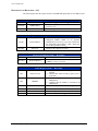
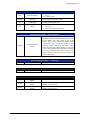
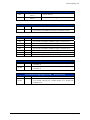
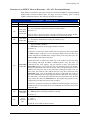
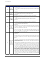
SM7000N SERIES
MICROWAVE SWITCH
USER’S
MANUAL
P/N: 82-0046-001
Released February 7, 2006
VXI Technology, Inc.
2031 Main St.
Irvine, CA 92614
(949) 955-1894
bus
www.vxitech.com
TABLE OF CONTENTS
INTRODUCTION
Certification .......................................................................................................................................................5
Warranty ............................................................................................................................................................5
Limitation of Warranty ......................................................................................................................................5
Restricted Rights Legend ...................................................................................................................................5
DECLARATION OF CONFORMITY ...............................................................................................................................6
GENERAL SAFETY INSTRUCTIONS .............................................................................................................................6
Terms and Symbols............................................................................................................................................7
Warnings ............................................................................................................................................................7
SUPPORT RESOURCES ...............................................................................................................................................9
SECTION 1..................................................................................................................................................................11
INTRODUCTION .......................................................................................................................................................11
Overview..........................................................................................................................................................11
Programming....................................................................................................................................................13
Automatic Scanning ...................................................................................................................................13
Programmable Timing Delays....................................................................................................................13
Safety Interrupt...........................................................................................................................................13
Break-Before-Make / Make-Before-Break Operation................................................................................13
SECTION 2..................................................................................................................................................................17
PREPARATION FOR USE ...........................................................................................................................................17
Introduction......................................................................................................................................................17
Calculating System Power and Cooling Requirements....................................................................................17
Setting the Chassis Backplane Jumpers ...........................................................................................................17
Setting the Logical Address .............................................................................................................................18
Selecting the Extended Memory Space............................................................................................................19
SECTION 3..................................................................................................................................................................21
PROGRAMMING .......................................................................................................................................................21
Register Access ................................................................................................................................................21
Addressing .......................................................................................................................................................21
Description of Registers - A16.........................................................................................................................23
Description of SMIP II Module Registers - A24 / A32 - Extended Memory .................................................32
DEVICE MEMORY MAP ...........................................................................................................................................35
Module Relay Control Address........................................................................................................................35
Relay Register Offset .......................................................................................................................................35
Writing to the Relays .......................................................................................................................................35
Programming....................................................................................................................................................36
SECTION 4..................................................................................................................................................................37
SWITCH CONFIGURATION .......................................................................................................................................37
Front Panel Connection - SM7000N................................................................................................................37
Switch Replacement.........................................................................................................................................44
Procedure....................................................................................................................................................44
PASS-THROUGH ADAPTERS ....................................................................................................................................46
Introduction......................................................................................................................................................46
Pass-Through Adapters - Connection Examples..............................................................................................48
INDEX .........................................................................................................................................................................51
Preface
3
VXI Technology, Inc.
4
Preface
www.vxitech.com
CERTIFICATION
VXI Technology, Inc. (VTI) certifies that this product met its published specifications at the time of shipment from
the factory. VTI further certifies that its calibration measurements are traceable to the United States National
Institute of Standards and Technology (formerly National Bureau of Standards), to the extent allowed by that
organization’s calibration facility, and to the calibration facilities of other International Standards Organization
members.
WARRANTY
The product module base SM7000N referred to herein is warranted against defects in material and workmanship for
a period of three years from the receipt date of the product at customer’s facility. The same warranty applies to the
switch options (SM72XXN) for a period of one year. The sole and exclusive remedy for breach of any warranty
concerning these goods shall be repair or replacement of defective parts, or a refund of the purchase price, to be
determined at the option of VTI.
For warranty service or repair, this product must be returned to a VXI Technology authorized service center. The
product shall be shipped prepaid to VTI and VTI shall prepay all returns of the product to the buyer. However, the
buyer shall pay all shipping charges, duties, and taxes for products returned to VTI from another country.
VTI warrants that its software and firmware designated by VTI for use with a product will execute its programming
when properly installed on that product. VTI does not however warrant that the operation of the product, or
software, or firmware will be uninterrupted or error free.
LIMITATION OF WARRANTY
The warranty shall not apply to defects resulting from improper or inadequate maintenance by the buyer, buyersupplied products or interfacing, unauthorized modification or misuse, operation outside the environmental
specifications for the product, or improper site preparation or maintenance.
VXI Technology, Inc. shall not be liable for injury to property other than the goods themselves. Other than the
limited warranty stated above, VXI Technology, Inc. makes no other warranties, express, or implied, with respect to
the quality of product beyond the description of the goods on the face of the contract. VTI specifically disclaims the
implied warranties of merchantability and fitness for a particular purpose.
RESTRICTED RIGHTS LEGEND
Use, duplication, or disclosure by the Government is subject to restrictions as set forth in subdivision (b)(3)(ii) of
the Rights in Technical Data and Computer Software clause in DFARS 252.227-7013.
VXI Technology, Inc.
2031 Main St.
Irvine, CA 92614 U.S.A.
Preface
5
VXI Technology, Inc.
DECLARATION OF CONFORMITY
Declaration of Conformity According to ISO/IEC Guide 22 and EN 45014
MANUFACTURER’S NAME
VXI Technology, Inc.
MANUFACTURER’S ADDRESS
2031 Main St.
Irvine, California 92614
PRODUCT NAME
Single Wide, Microwave Switch Base Module
MODEL NUMBER(S)
SM7000N
PRODUCT OPTIONS
All
PRODUCT CONFIGURATIONS
All
VXI Technology, Inc. declares that the aforementioned product conforms to the requirements of
the Low Voltage Directive 73/23/EEC and the EMC Directive 89/366/EEC (inclusive 93/68/EEC)
and carries the “CE” mark accordingly. The product has been designed and manufactured
according to the following specifications:
SAFETY
EN61010 (2001)
EMC
EN61326 (1997 w/A1:98) Class A
CISPR 22 (1997) Class A
VCCI (April 2000) Class A
ICES-003 Class A (ANSI C63.4 1992)
AS/NZS 3548 (w/A1 & A2:97) Class A
FCC Part 15 Subpart B Class A
EN 61010-1:2001
The product was installed into a C-size VXI mainframe chassis and tested in a typical configuration.
I hereby declare that the aforementioned product has been designed to be in compliance with the relevant sections
of the specifications listed above as well as complying with all essential requirements of the Low Voltage Directive.
February 2006
Steve Mauga, QA Manager
6
Preface
www.vxitech.com
GENERAL SAFETY INSTRUCTIONS
Review the following safety precautions to avoid bodily injury and/or damage to the product.
These precautions must be observed during all phases of operation or service of this product.
Failure to comply with these precautions, or with specific warnings elsewhere in this manual,
violates safety standards of design, manufacture, and intended use of the product.
Service should only be performed by qualified personnel.
TERMS AND SYMBOLS
These terms may appear in this manual:
WARNING
Indicates that a procedure or condition may cause bodily injury or death.
CAUTION
Indicates that a procedure or condition could possibly cause damage to
equipment or loss of data.
These symbols may appear on the product:
ATTENTION - Important safety instructions
Frame or chassis ground
Indicates that the product was manufactured after August 13, 2005. This mark is
placed in accordance with EN 50419, Marking of electrical and electronic
equipment in accordance with Article 11(2) of Directive 2002/96/EC (WEEE).
End-of-life product can be returned to VTI by obtaining an RMA number. Fees
for take-back and recycling will apply if not prohibited by national law.
WARNINGS
Follow these precautions to avoid injury or damage to the product:
Preface
Use Proper Power Cord
To avoid hazard, only use the power cord specified for this product.
Use Proper Power Source
To avoid electrical overload, electric shock, or fire hazard, do not
use a power source that applies other than the specified voltage.
Use Proper Fuse
To avoid fire hazard, only use the type and rating fuse specified for
this product.
7
VXI Technology, Inc.
WARNINGS (CONT.)
Avoid Electric Shock
To avoid electric shock or fire hazard, do not operate this product
with the covers removed. Do not connect or disconnect any cable,
probes, test leads, etc. while they are connected to a voltage source.
Remove all power and unplug unit before performing any service.
Service should only be performed by qualified personnel.
Ground the Product
This product is grounded through the grounding conductor of the
power cord. To avoid electric shock, the grounding conductor must
be connected to earth ground.
Operating Conditions
To avoid injury, electric shock or fire hazard:
Do not operate in wet or damp conditions.
Do not operate in an explosive atmosphere.
Operate or store only in specified temperature range.
Provide proper clearance for product ventilation to prevent
overheating.
DO NOT operate if you suspect there is any damage to this
product. Product should be inspected or serviced only by
qualified personnel.
The operator of this instrument is advised that if equipment is
used in a manner not specified in this manual, the protection
provided by this equipment be may be impaired.
Improper Use
8
Preface
www.vxitech.com
SUPPORT RESOURCES
Support resources for this product are available on the Internet and at VXI Technology customer
support centers.
VXI Technology
World Headquarters
VXI Technology, Inc.
2031 Main Street
Irvine, CA 92614-6509
Phone: (949) 955-1894
Fax: (949) 955-3041
VXI Technology
Cleveland Instrument Division
5425 Warner Road
Suite 13
Valley View, OH 44125
Phone: (216) 447-8950
Fax: (216) 447-8951
VXI Technology
Lake Stevens Instrument Division
VXI Technology, Inc.
1924 - 203 Bickford
Snohomish, WA 98290
Phone: (425) 212-2285
Fax: (425) 212-2289
Technical Support
Phone: (949) 955-1894
Fax: (949) 955-3041
E-mail: [email protected]
Visit http://www.vxitech.com for worldwide support sites and service plan information.
Preface
9
VXI Technology, Inc.
10
Preface
www.vxitech.com
SECTION 1
INTRODUCTION
OVERVIEW
The SM7000N Microwave Switch Module is a member of the VXI Technology SMIP II™
family, which offers a modular design allowing custom switching configurations.
The SM7000N is a single-wide, C-size VXI module, which can support up to six different
microwave switches in any combination of SPDT through SP6T relays. Blanking plates cover any
unused switch positions (see Figure 1-1).
FIGURE 1-1: SM7000N MICROWAVE SWITCH MODULE
SM7000N Introduction
11
VXI Technology, Inc.
Using the SMIP II family for microwave switching, the user obtains the following benefits over
other VXI microwave switch solutions:
Density
Up to six (1 x 6) microwave relays can be housed in a single VXIbus
slot.
Modularity
Each SM7000N switch module can house up to six switches, or
“building blocks”, which can be mixed and matched for the final
configuration. There are eight of these “building blocks” from which
to chose.
The following table lists the different switch available in the SM7000N series.
SM7000N SERIES SWITCH OPTIONS
MODEL DC – 18 GHZ
SM7270N
SM7272N
SM7274N
SM7275N
SM7276N
Model DC – 26.5 GHz
SM7282N
SM7284N
12
Relay Type
Dual SPDT Non-latching
SP4T Non-latching
SP6T Non-latching
Mini Transfer Switch
Pass-Through Adapter
Relay Type
SP4T Non-latching
SP6T Non-latching
SM7000N Introduction
www.vxitech.com
PROGRAMMING
The SMIP II family of switch modules is programmed using direct register access for fast data
throughput.
Automatic Scanning
A predefined sequence of channels can be programmed into an extensive scan list that can be
incremented by a trigger. This approach relieves the host controller from having to tie up the
VXIbus backplane when scanning.
Programmable Timing Delays
A delay can be programmed between relay closures to allow for settling times of other system
resources. When used with triggers, a controlled synchronous switching system can easily be
configured.
Safety Interrupt
This is a programmable fail-safe feature that allows all relays to open based upon the occurrence
of a selected TTL backplane trigger. This allows signals to be removed from the unit under test if
a system fail-safe occurs, such as inadvertent removal of a test adapter.
Break-Before-Make / Make-Before-Break Operation
This feature allows automatic Break-Before-Make (BBM) and Make-Before-Break (MBB)
operations. It is programmed simply by setting user configurable options. In BBM operation, all
opening relays are guaranteed to open prior to any closing relays being set. The relay open or
close time is user configurable as well. In MBB operation, the closing relays are guaranteed to be
set prior to the opening relays being opened.
SM7000N Introduction
13
VXI Technology, Inc.
TABLE 1-1: SM7000N SPECIFICATIONS
SM7000N SPECIFICATIONS
RF PERFORMANCE
Frequency (GHz)
VSWR
Insertion Loss (dB max)
Isolation (dB min)
ADDITIONAL SPECIFICATIONS
RF Impedance
Actuating Voltage
Actuating Current
Switching Time
Switching Sequence
Operating Ambient Temperature
Operating Life
DC – 3
1.15:1
0.15
85
3–8
1.25:1
0.25
75
8 – 12.4
1.35:1
0.35
65
12.4 – 18
1.45:1
0.45
65
18 – 26.5
1.9:1
0.8
45
50 Ω nominal
24 VDC
Normally open: 350 mA (maximum)
15 ms (maximum)
Break-Before-Make
-35°C to +70°C
One million cycles per position
AVERAGE POWER (Watts)
TABLE 1-2: POWER VS. FREQUENCY GRAPH FOR SWITCHES
1000
900
800
700
600
500
400
300
200
ST
AN
DA
RD
100
90
80
70
60
SM
A
50
40
0.1
0.2
0.3 0.4 0.5 0.6 0.8
1
2
3
4
5 6
8
10 12.4
18
26.5
FREQUENCY (GHz)
14
SM7000N Introduction
www.vxitech.com
TABLE 1-3: INSERTION, ISOLATION & RETURN LOSS GRAPHS FOR SWITCHES
SM7000N Introduction
15
VXI Technology, Inc.
16
SM7000N Introduction
www.vxitech.com
SECTION 2
PREPARATION FOR USE
INTRODUCTION
When the SMIP II is unpacked from its shipping carton, the contents should include the following
items:
(1) SMIP II VXIbus module
(1) SM7000N Series Microwave Switch User’s Manual (this manual)
All components should be immediately inspected for damage upon receipt of the unit.
Once the SMIP II is assessed to be in good condition, it may be installed into an appropriate Csize or D-size VXIbus chassis in any slot other than slot zero. The chassis should be checked to
ensure that it is capable of providing adequate power and cooling for the SMIP II. Once the
chassis is found adequate, the SMIP’s logical address and the chassis’ backplane jumpers should
be configured prior to the SMIP’s installation.
CALCULATING SYSTEM POWER AND COOLING REQUIREMENTS
It is imperative that the chassis provide adequate power and cooling for this module. Referring to
the chassis operation manual, confirm that the power budget for the system (the chassis and all
modules installed therein) is not exceeded and that the cooling system can provide adequate
airflow at the specified backpressure.
It should be noted that if the chassis cannot provide adequate power to the module, the instrument
may not perform to specification or possibly not operate at all. In addition, if adequate cooling is
not provided, the reliability of the instrument will be jeopardized and permanent damage may
occur. Damage found to have occurred due to inadequate cooling would also void the warranty of
the module.
SETTING THE CHASSIS BACKPLANE JUMPERS
Please refer to the chassis operation manual for further details on setting the backplane jumpers.
SM7000N Preparation for Use
17
VXI Technology, Inc.
SETTING THE LOGICAL ADDRESS
The logical address of the SMIP II is set by two rotary switches located on the top edge of the
interface card, near the backplane connectors. Each switch is labeled with positions 0 through F.
The switch closer to the front panel of the module is the least significant bit (LSB or “Front”),
and the switch located towards the back of the module is the most significant bit (MSB or
“Back”). To set the Logical Address (LA), simply rotate the pointer to the desired value. For
example, to set the LA to 25, first convert the decimal number to the hexadecimal value of 19.
Next, set the back switch to 1, and the front switch to 9. See Figure 2-1. Two examples are
provided below:
Example 1
=
1
w/ 9 remaining
Divide the decimal value by 16 to get
the MSB and the LSB.
=
0001
1001
The 1 is the MSB, and the remainder of
9 is the LSB.
=
1
9
Convert to hexadecimal. Set the back
switch to 1 and the front switch to 9.
FRONT
3456
3456
789A
78 9A
F0 12
BACK
F012
25 / 16
LSB
BC
25
MSB
DE
Divide
by 16
BC
LA
(decimal)
DE
FIGURE 2-1: LOGICAL ADDRESS EXAMPLE 1
18
SM7000N Preparation for Use
www.vxitech.com
Example 2
200 / 16
LSB
=
12
w/ 8 remaining
Divide by 16.
=
1100
1000
Convert to MSB and LSB.
=
C
8
Convert to hexadecimal. Set the back
switch to C and the front switch to 8.
BACK
FRONT
3456
3456
789A
789A
F0 12
200
MSB
F0 12
Divide
by 16
D
BC E
LA
(decimal)
D
BC E
FIGURE 2-2: LOGICAL ADDRESS EXAMPLE 2
Here is another way of looking at the conversion:
LA = (back switch x 16) + front switch
LA = (1 x 16) + 9
LA = 16 + 9
LA = 25
Set the address switches to FF for dynamic configuration. Upon power-up, the resource manager
will assign a logical address. See Section F - Dynamic Configuration in the VXIbus Specification
for further information.
There is only one logical address per SMIP II base unit. Address assignments for individual
modules are handled through the A24/A32 address space allocation.
SELECTING THE EXTENDED MEMORY SPACE
The Extended Memory Space of the SMIP II is set by a DIP switch that is located on the bottom
edge of the interface card. Position 1, located to the left on the DIP switch, selects between A24
and A32 memory address space. In the UP position, the SMIP II will request A24 space. In the
DOWN position, the SMIP II will request A32 space. (Position 2 is not currently used.) The
selection of the address space should be based upon the memory allocation requirements of the
system that the SMIP II module will be installed. The amount of memory allocated to the SMIP II
module is independent of the address space selected.
SM7000N Preparation for Use
19
VXI Technology, Inc.
20
SM7000N Preparation for Use
www.vxitech.com
SECTION 3
PROGRAMMING
REGISTER ACCESS
The SMIP II modules are VXIbus register-based devices for high-speed data retrieval. Registerbased programming is a series of reads and writes directly to the switch module registers. This
eliminates the time for command parsing thus increasing speed.
ADDRESSING
The VTI switching modules utilize either the A24 or A32 space of the shared-memory
architecture. To read or write to a module register, a register address needs to be specified. This is
done by using the offset value (assigned by the resource manager) and multiplying it by 256 or
64k to get the base address in A24 or A32 address space, respectively
A24 Base Address = Offset value * 0x00FF (or 256)
A32 Base Address = Offset value * 0xFFFF (or 65,535)
The A24 or A32 offset value, assigned by the resource manager, can also be accessed by reading
the A16 Offset Register. To address the A16 Offset Register use the following formula:
A16 Base Address = (Logical Address * 64) + 0xC000 (or 49,152)
then
A16 Offset Register Address = A16 Base Address + 6
See following for the A16 Memory Map and the A24/A32 address space allocation.
SM7000N Programming
21
VXI Technology, Inc.
TABLE 3-1: SMIP II™ REGISTER MAP - A16
OFFSET
WRITE FUNCTION
READ FUNCTION
0x3E
0x3C
0x3A
0x38
0x36
0x34
0x32
0x30
0x2E
0x2C
0x2A
0x28
0x26
0x24
0x22
0x20
0x1E
0x1C
0x1A
0x18
0x16
0x14
0x12
0x10
0x0E
0x0C
0x0A
0x08
0x06
0x04
0x02
0x00
Trace Advance
Busy Trigger Control
Trace RAM Control
TTL Trigger Polarity
Open Trigger Select
Trace ADV Trigger Select
Trace RAM Address LOW
Trace RAM Address HIGH
Trace RAM End LOW
Trace RAM End HIGH
Trace RAM Start LOW
Trace RAM Start HIGH
Module 5, 4 Used Address
Module 3, 2 Used Address
Module 1, 0 Used Address
NVM Access Register
Reserved
Interrupt Control
Reserved
Reserved
Reserved
Reserved
Reserved
Reserved
Reserved
Reserved
Reserved
Reserved
Offset Register
Control Register
Reserved
LA Register
Board Busy
Busy Trigger Control
Trace RAM Control
Reserved
Reserved
Reserved
Trace RAM Address LOW
Trace RAM Address HIGH
Trace RAM End LOW
Trace RAM End HIGH
Trace RAM Start LOW
Trace RAM Start HIGH
Reserved
Reserved
Reserved
NVM Access Register
Subclass Register
Interrupt Control
Interrupt Status
Reserved
Reserved
Reserved
Reserved
Reserved
Version Number
Serial Number LOW
Serial Number HIGH
Reserved
Offset Register
Status Register
Device Type Register
ID Register
NOTE As members of the SMIP II series, the SM7000N Series microwave modules allocate for six (6) module
boards, but only implement Module 0. Modules 1 - 5 are unused.
22
SM7000N Programming
www.vxitech.com
DESCRIPTION OF REGISTERS - A16
The following describes the registers shown in the SMIP II Register Map for A16 address space.
ID Register (0x00) — Read Only
D11-D0
Manufacturer's ID
D13-D12
Address Space
D15-D14
Device Class
VXI Technology, Inc., set to F4B16
A16/A24 = 002
A16/A32 = 012
Extended register based device, set to 012
Logical Address Register (0x00) — Write Only
D7-D0
Logical Address
D15-D8
Reserved
Sets the new logical address in a dynamically
configured module. When set for dynamic
configuration (set to FF16) a soft reset will not alter
the configured logical address, while a hard reset
will set the register back to FF16.
Writing to this range has no effect.
Device Type Register (0x02) — Read Only
D11-D0
Model Code
D15-D12
Required Memory
Model 277, set to 11516
2 Mbytes, set to 216, for A24
2 Mbytes, set to A16, for A32
Status Register (0x04) — Read Only
1 = indicates that A24/A32 memory space access is
enabled
0 = indicates that A24/A32 memory space access is
locked out
1 = indicates that the module is not selected by the
MODID line
0 = indicates that the module is selected by the
MODID line.
These bits always read as 11,1111,11112
D15
A24/A32 Active
D14
MODID*
D13-D4
Reserved
D3
Ready
This bit always reads as 12
D2
Passed
This bit always reads as 12
D1-D0
Reserved
SM7000N Programming
These bits always read as 112
23
VXI Technology, Inc.
Control Register (0x04) — Write Only
D15
A24/A32 Enable
D14-D2
Reserved
D1
Sysfail Inhibit
D0
Reset
1 = write a 1 to this bit to enable A24/A32 memory
access
0 = to disable access
Writes to these bits have no effect.
Write a 1 to this bit to prevent the module from
asserting the SYSFAIL* line.
1 = write a 1 to this bit to force the module into a
reset state
0 = write a 0 to release the reset state
Offset Register (0x06) — Read and Write
D15-D0
A24/A32 Memory
Offset
The value written to this 16-bit register, times 256,
sets the base address of the A24 memory space used
by the module. The value written to this 16-bit
register, times 65,536, sets the base address of the
A32 memory space used by the module. A read
from this register reflects the previously written
value. Because of the required memory size, bits D4
- D0 are disregarded on writes and always read back
as 0. Upon receiving a hard reset, all bits in this
register are set to 0. A soft reset does not affect the
value in this register.
Reserved Register (0x0A) — Read Only
D15-D0
Not Implemented
Always read back as FFFF16
Reserved Register (0x0C) — Read Only
D15-D0
Not Implemented
Always read back as FFFF16
Version Number Register (0x0E) — Read Only
D15-D8
D7-D4
D3-D0
24
Firmware Version
Number
Major Hardware Version
Number
Minor Hardware Version
Number
Not applicable, reads back as 0016
Depends on the specific hardware revision of the
SMIP II interface board.
Depends on the specific hardware revision of the
SMIP II interface board.
SM7000N Programming
www.vxitech.com
Interrupt Status Register (0x1A) — Read Only
D15
Scan Function done
D14
Openbus Active Event
true
D13-D8
Modules 0 - 5 Busy
complete
The latest scan list update is complete.
The Openbus was activated by one or more
programmed inputs. See description of the Openbus
in the module register section.
D13 = Module 5, D12 = Module 4, … and D8 =
Module 0.
The programmed Busy signal from one of the
modules has timed out. This indicates that the relays
actuated for that Busy cycle have settled and a
measurement may take place.
D7-D0
Reserved
Always reads back as FFFF16
NOTE This status register may be used in a polled fashion rather than allowing the events
above to generate an Interrupt. A read of this register will clear any active bits. Bits that
are not set, or are about to be set are not affected by a read of this register.
Interrupt Control Register (0x1C) — Read and Write
D15
D14
D13-D8
Scan Function done
mask bit
Openbus Active Event
true mask bit
Module 0 - 5 Busy
complete
0 = enabled
1 = disabled
0 = enabled
1 = disabled
0 = enabled
1 = disabled
D13 = Module 5, D12 = Module 4, … and D8 =
Module 0.
0 = writing a 0 to this bit enables interrupter
capabilities
D7
IR ENA*
1 = writing a 1 to this bit disables interrupter
capabilities
The module has no interrupt handler capability;
D6
IH ENA*
therefore writing a 1 or 0 has no effect. A 1 is
always read back for this bit.
The complement of the value programmed into
these three bits reflects the selected IRQ line used
D5-D3
Interrupter IRQ Line
by the module. A value of 0112 would select IRQ4,
a value of 0002 would select IRQ7, and a value of
1112 would disconnect the IRQ lines.
The module has no interrupt handler capability;
D2-D0
Handler IRQ Line
therefore writing to these bits has no effect. A 1112
is always read back for these bits.
Note that all bits in this register are set to 1 upon receipt of a hard or soft reset.
SM7000N Programming
25
VXI Technology, Inc.
Subclass Register (0x1E) — Read Only
D15
D14-D0
VXIbus Extended
Device
Extended Memory
Device
Always reads as 1.
Always reads as 7FFD16
NVM Access Resister (0x20) — Read Only
D15-D1
Unused
D0
All Bits are always 1.
Reads back the serial data stream from the selected SMIP II board.
Note that only one SMIP II board may be read back at a time.
NVM Access Resister (0x20) — Write Only
D15-D7
Unused
Data written to these bits have no effect.
D6
Serial clock for module 5; should be a logic 1 when not used.
D5
Serial clock for module 4; should be a logic 1 when not used.
D4
Serial clock for module 3; should be a logic 1 when not used.
D3
Serial clock for module 2; should be a logic 1 when not used.
D2
Serial clock for module 1; should be a logic 1 when not used.
D1
Serial clock for module 0; should be a logic 1 when not used.
D0
Serial data input for all modules; must be a logic 1 when not used.
Board X, Y Used Address Register (0x22, 0x24, 0x26) — Read and Write
Sets the actual number of words of address space used by the relays
on board's X.
Sets the actual number of words of address space used by the relays
on board's Y.
D15-D8
D7-D0
Trace RAM Start High Register (0x28) — Read and Write
D15-D4
D3-D0
26
Unused
Data written to these bits have no effect and always read back as 1.
Sets the four most significant bits of the starting address of the
Trace RAM, allowing the available RAM to be divided into
multiple traces.
SM7000N Programming
www.vxitech.com
Trace RAM Start Low Register (0x2A) — Read and Write
Sets the 16 least significant bits of the starting address of the Trace
RAM, allowing the available RAM to be divided into multiple
traces.
D15-D0
Trace RAM End High Register (0x2C) — Read and Write
D15-D4
Unused
D3-D0
Data written to these bits have no effect and always read back as 1.
Sets the four most significant bits of the ending address of the
Trace RAM, allowing the available RAM to be divided into
multiple traces.
Trace RAM End Low Register (0x2E) — Read and Write
Sets the 16 least significant bits of the ending address of the Trace
RAM, allowing the available RAM to be divided into multiple
traces.
D15-D0
Trace RAM Address HIGH Register (0x30) — Read and Write
D15-D4
Unused
D3-D0
Data written to these bits have no effect and always read back as 1.
Sets and reads back the four most significant bits of the current
address of the Trace RAM, allowing the current trace RAM address
to be queried and changed.
Trace RAM Address LOW Register (0x32) — Read and Write
Sets and reads back the sixteen least significant bits of the current
address of the Trace RAM, allowing the current trace RAM address
to be queried and changed.
D15-D0
Trace Advance Trigger Select Register (0x34) —Write Only
D15-D8
D7-D0
SM7000N Programming
Sets the TTLTRIG line or lines, which are configured as outputs,
and will toggle when Trace Advance condition occurs in the
module. D15 corresponds to TTLTRIG7, D14 to TTLTRIG6, …
and D8 to TTLTRIG0. Setting a bit to a 1 enables the trigger line,
setting a bit to 0 disables the corresponding line. All bits are set to 0
when either a soft or a hard reset is received by the module.
Sets the TTLTRIG line or lines, which are configured as inputs, and
will cause a Trace Advance event to occur in the module. D7
corresponds to TTLTRIG7, D6 to TTLTRIG6, … and D0 to
TTLTRIG0. Setting a bit to a 1 enables the trigger line, setting a bit
to 0 disables the corresponding line. All enabled TTLTRIG lines
are OR'd together to allow more than one TTLTRIG line to cause a
Trace Advance event to occur. All bits are set to 0 when the module
receives either a soft or a hard reset.
27
VXI Technology, Inc.
Open Trigger Select Register (0x36) —Write Only
Sets the TTLTRIG line or lines, which are configures as outputs,
and will toggle when Relay Open condition occurs in the module.
D15 corresponds to TTLTRIG7, D14 to TTLTRIG6, … and D8 to
TTLTRIG0. Setting a bit to a 1 enables the trigger line, setting a bit
to 0 disables the corresponding line. All bits are set to 0 when either
a soft or a hard reset is received by the module.
Sets the TTLTRIG line or lines, which are configured as inputs, and
will cause a Relay Open event to occur in the module. D7
corresponds to TTLTRIG7, D6 to TTLTRIG6, … and D0 to
TTLTRIG0. Setting a bit to a 1 enables the trigger line, setting a bit
to 0 disables the corresponding line. All enabled TTLTRIG lines
are OR'd together to allow more than one TTLTRIG line to cause a
Relay Open event to occur. All bits are set to 0 when the module
receives either a soft or a hard reset.
D15-D8
D7-D0
TTL Trigger Polarity Register (0x38) —Write Only
D15-D14
Unused
D13-D8
FAIL LED Control
Data written to these bits have no effect.
D13 is for module 5, D12 is for module 4, … D8 is for
module 0. 0 = Off, 1 = On.
Board Busy
0 acts on the falling edge, 1 acts on the rising edge.
Trigger Slope
Relay Open Input
D3
0 acts on the falling edge, 1 acts on the rising edge.
Slope
Relay Open Output
D2
0 sets the falling edge active, 1 sets the rising edge active.
Slope
Trace Advance
0 advances on the falling edge, 1 advances on the rising
D1
Input Slope
edge.
Trace Advance
D0
0 sets the falling edge active, 1 sets the rising edge active.
Output Slope
NOTE: A hard or a soft reset sets D3 - D0 to 0.
D4
28
SM7000N Programming
www.vxitech.com
Trace RAM Control Register (0x3A) — Read and Write
D15-D10
Modules Installed
D9-D4
Modules used in
trace mode
D3-D2
Unused
D1
LOOP ENABLE
D0
TRACE ENABLE
D15 is for module 5, D10 is for module 0. Set to 0 if the
module is installed or set to a 1 if not installed. These bits
are set to 0 at power on. By setting a 1, the SMIP II
Interface PCB will generate DTACK for any read or
write cycles to the memory space of the uninstalled plugin modules.
D9 is for module 5, D4 is for module 0. Set to 1 if the
module is used in trace mode, set to 0 if not in trace
mode.
Data written to these bits have no effect. The value
written is read back.
1 = Enabled, 0 = Disabled. If enabled, the trace resumes
at the start of active RAM and continues from there. If
disabled, the trace stops at the end of active RAM and
clears the TRACE ENABLE bit.
1 = enabled, 0 = disabled. If the LOOP ENABLE bit is
set and the end of active trace RAM is reached, this bit
will not be reset.
Busy Trigger Control Register (0x3C) — Read and Write
D15-D8
TTLTRIG
Select
D7-D6
Unused
D5-D0
Busy
Trigger
Enable
Sets the TTLTRIG Line or Lines, which are configured as outputs,
and will toggle at the de-assertion of a Board Busy condition sent
by the plug-in modules. D15 corresponds to TTLTRIG7, D14 to
TTLTRIG6, … and D8 to TTLTRIG0. Setting a bit to a 1 enables
the trigger line, setting a bit to a 0 disables the corresponding line.
All bits are set to 0 when either a soft or a hard reset is received by
the module.
Data written to these bits have no effect. The value written is read
back.
Enables the Board Busy signals received from the plug-in modules
to generate a trigger condition on the TTL Trigger Bus. D5
corresponds to Board Busy Module 5, D4 to Board Busy Module 4,
… and D0 to Board Busy Module 0. Setting a bit to a 1 enables the
generation of a Trigger condition; setting a bit to a 0 disables the
corresponding line. All bits are set to 0 when either a soft or a hard
reset is received by the module.
Software can be written to enable the last board updated to generate
the TTLTrigger condition, alerting any other instruments that the
plug-in modules' relays have settled. Alternatively, all of the plugin modules may be enabled to generate the TTLTrigger condition.
Trigger Advance Register (0x3E) — Write Only
D15-D0
Unused
SM7000N Programming
The act of writing to this location causes a Trace Advance event to
occur in the module. The specific data written to these bits has no
effect.
29
VXI Technology, Inc.
Board Busy Register (0x3E) — Read Only
D15-D7
Unused
D6
D5
D4
D3
D2
D1
D0
These bits always read back as 1.
Indicates whether the SMIP II platform is a single or double wide.
0 = single wide
1 = double wide
A 0 read from this bit indicates the relays on module 5 have settled,
a 1 indicates that the relays on module 5 are still changing state.
A 0 read from this bit indicates the relays on module 4 have settled,
a 1 indicates that the relays on module 4 are still changing state.
A 0 read from this bit indicates the relays on module 3 have settled,
a 1 indicates that the relays on module 3 are still changing state.
A 0 read from this bit indicates the relays on module 2 have settled,
a 1 indicates that the relays on module 2 are still changing state.
A 0 read from this bit indicates the relays on module 1 have settled,
a 1 indicates that the relays on module 1 are still changing state.
A 0 read from this bit indicates the relays on module 0 have settled,
a 1 indicates that the relays on module 0 are still changing state.
Reserved Registers — Read and Write
D15-D0
30
Unused
Writing to these registers has no effect and will always read back as
FFFF16.
SM7000N Programming
www.vxitech.com
1M Memory
Allocated to Store
Module Settings
1MB RAM
VXI Configuration Space
2MB of A24 or A32
Address Space Reserved
for VTI SMIP Module
(Assigned by the Controller)
Unused
1MB RAM
Module 5 Configuration - 512 bytes
1KB Each Module
Module 5 Relays - 512 bytes
Module 4 Configuration - 512 bytes
1M Memory
Allocated for
Configuration/
Relay Registers
1K Each Module
Configuration Space
Switch Module Specific
Configuration Registers
Module 4 Relays - 512 bytes
Module 3 Configuration - 512 bytes
Module 3 Relays - 512 bytes
Module 2 Configuration - 512 bytes
Module 2 Relays - 512 bytes
Module 1 Configuration - 512 bytes
Module 1 Relays - 512 bytes
Module 0 Configuration - 512 bytes
Relay Space
Utilized as shown
in the Relay Register Map
(See Module Appendices)
Module 0 Relays - 512 bytes
FIGURE 3-1: A24/A32 ADDRESS SPACE
NOTE
As members of the SMIP II series, the SM7000 Series microwave switch modules allocate for
six (6) module boards, but only implement Module 0. Modules 1 - 5 are unused.
SM7000N Programming
31
VXI Technology, Inc.
DESCRIPTION OF SMIP II MODULE REGISTERS - A24 / A32 - EXTENDED MEMORY
Each module is assigned 1k (1024) bytes of memory as shown in the SMIP II Configuration/Relay
Register Map for A24/A32 address space. The upper 512 bytes of memory space is used for
module configuration registers. The following describes these registers.
Control Register — Read and Write
ADDR
D15-D10
D9
D8
Plug-In LA+0x200
Unused
Relay Data
Read Back
Polarity Bit
ACFAILN
Enable Bit
0 = Normal polarity relay data is read back from this module
1 = Inverted polarity relay data is read back from this module
Pon state = 0
This bit may be used to invert the relay data read back from the plug-in module.
Control, Delay, and Status Register read backs are not effected by this bit.
0 = ACFAILN is enabled to reset this module's relays
1 = ACFAILN is disabled from resetting this module's relays
Pon state = 0
0 = BBM (Break-Before-Make) / MBB (Make-Before-Break) operation on this
plug-in module is disabled
1 = BBM/MBB operation on this plug-in module is enabled
Pon state = 0
If this bit is set, the relays on this module will be sequenced to effect proper BBM
or MBB operation. If this bit is not set, the plug-in module will process the newly
written relay data as immediate data, writing it directly to the relay driver ports. No
BBM or MBB sequencing will take place.
D7
D6
D5
BBM/MBB
Enable Bit
BBM/MBB
Select Bit
Access
LED Fail
Bit
While this feature is enabled, the initial write to the module will start the delay
timer running and begin the BBM or MBB operation. Since the relays are
controlled by the 16-bit registers, only the effected 16 relays will perform the
BBM/MBB operation. To overcome this fact, any subsequent writes to the module,
during the initial delay timer time-out period, will be accepted and processed. In
addition, the delay time will be reset and begin counting down again. Once the
delay timer has timed-out (this indicates that the relays have settled into their
BBM/MBB state), writes to the module will not be accepted and may result in a
Bus Error depending on the value programmed into the delay timer. This is because
the delay timer is reset at the end of the initial time-out and is used to time the final
relay closure into their post BBM/MBB state. The module Busy signal will only
complete once the final relay closure state is reached.
If this bit is set and no value has been loaded into the Delay Register, the plug-in
module will act as if this enable bit is not set and load all of the relay drivers with
immediate data.
0 = BBM operation on this plug-in module is selected
1 = MBB operation on this plug-in module is selected
Pon state = 0
0 = Inactive
1 = Active
Pon state = 0
Lights the Access LED red when activated.
32
SM7000N Programming
www.vxitech.com
Control Register — Read and Write (Continued)
D4
D3
D2
Relay
Reset
Enable Bit
Relay
Reset
Select Bit
Openbus
Out Enable
Bit
0 = The Openbus and Front Panel Open signals are not enabled to reset this
module's relays
1 = The Openbus or Front Panel Open signal may be selected to reset this module's
relays
Pon state = 0
0 = Front Panel Open signal is selected to reset this module's relays
1 = The Openbus signal is selected to reset this module's relays
Pon state = 0
Many plug-in modules may be programmed to be listeners on the Openbus.
0 = Disables this module's Front Panel Open signal from driving the Openbus
signal
1 = Enables this module's Front Panel Open signal to drive the Openbus
Pon state = 0
Many plug-in modules may be programmed to be talkers on the Openbus.
0 = Non-inverted Front Panel Open signal polarity
1 = Inverted Front Panel Open signal polarity
Pon state = 0
D1
Front Panel
Open
Signal
Polarity Bit
Non-inverted: If set in pulse mode, the Front Panel Open signal will generate a
reset pulse on a falling edge. If set in level mode, the Front Panel Open signal will
generate a reset signal on a low input signal.
Inverted: If set in pulse mode, the Front Panel Open signal will generate a reset
pulse on a rising edge. If set in level mode, the Front Panel Open signal will
generate a reset signal on a high input signal.
0 = Pulse mode
1 = Level mode
Pon state = 0
Pulse mode: An edge seen at the Front Panel Open signal pin will generate a reset
pulse that may be used to reset system relays. The pulse is of approximately 300 ns
duration.
D0
Front Panel
Open
Signal
Operation
Select Bit
SM7000N Programming
Level mode: A level present on the Front Panel Open signal pin will generate a
reset signal that may be used to reset system relays. This signal will remain active
as long as the input is active.
On the front panel of most SMIP II plug-in modules, there are two pins for access
to the module's Front Panel Open signal. These are the Front Panel Open signal pin
and a ground reference pin. The purpose of the Front Panel Open signal is to allow
user access to a configurable interlock feature that will reset all of the SMIP II
system relays. The Front Panel Open signal may be used to reset the relays only on
the module, which initiated the Front Panel Open signal fault condition. It also may
be used to broadcast to all the other SMIP II plug-in modules installed in a SMIP II
Interface Module via what is called the Openbus. Any plug-in module may be
programmed to drive and/or listen to the Openbus. The Openbus signal may also be
used to generate a wider chassis level fault signal via the TTL Trigger Bus (see the
register definitions for A16 address space). The Front Panel Open signal is meant
to be driven by either a switch closure or TTL/CMOS logic gate. It is pulled high
on the module.
33
VXI Technology, Inc.
Delay Register — Read and Write
ADDR
D15-D0
Plug-In LA+0x202
This register is used to set the time that the plug-in module will hold the Board
Busy signal active. The Board Busy signal is set every time the plug-in receives a
Write to a relevant Relay Register memory space. The Board Busy signal will be
removed at the end of the time out that is set by the value contained in this register.
For each count loaded into this register, the Board Busy signal will be held active
for 1 µs. The delay may be set from 0 to approximately 65 ms, thus accommodating
Data Bus
a wide variation in test station requirements.
16 Bit
The Board Busy signal may be monitored by the user, in either a polled or an
interrupt fashion, and is to be used as an indication that the relays in the newly
actuated path have settled. Alternatively, the Board Busy signal may also be used to
drive the TTL Trigger Bus. See the Board Busy, Interrupt Control and Busy
Trigger Control Register descriptions in the A16 address space.
Status Register — Read Only
ADDR
D15-D13
D12-D1
D0
34
Plug-In LA+0x204
Hardware
Revision
Code
Unused
Reserved for future use.
0 = Indicates that this module's Front Panel Open signal was not activated by the
user
1 = An indication that this module's Front Panel Open signal was activated as
Front Panel
programmed by the user
Open
Pon state = 0
signal set
by this
A read of this bit location will indicate whether the Front Panel Open signal was
module
triggered from this plug-in module's front panel. In the event that multiple talkers
have been programmed to drive the Openbus signal, this bit may be queried by the
user to discover which module's Front Panel Open signal caused the Openbus
Active Event to occur. A read of this register clears this bit to 0.
SM7000N Programming
www.vxitech.com
DEVICE MEMORY MAP
MODULE RELAY CONTROL ADDRESS
Each module is assigned 1k (1024) bytes of memory as shown in the SMIP II Configuration/Relay
Register Map for A24/A32 address space. The lower 512 bytes of each module's memory is used
for relay control. Each module is assigned its own base address. These base addresses are in 1K
increments as follows:
Module 0 (J100) Base Address = H0000
Module 1 (J101) Base Address = H0400
Module 2 (J102) Base Address = H0800
Module 3 (J103) Base Address = H0C00
Module 4 (J104) Base Address = H1000
Module 5 (J105) Base Address = H1400
NOTE
The SM7000N microwave module, being a member of the SMIP II series, allocates for six (6)
module boards, but only implements Module 0. Modules 1 - 5 are unused.
The Module Base Address is then added to the A24/A32 Base Address to access a specific
module's relays:
Module Relay Address = A24/A32 Base Address + Module Base Address
RELAY REGISTER OFFSET
The Relay Register Offset is located within the module's A24/32 address space. When you send
data to the register, the relay register offset is added to the A24/A32 base address and module base
address:
Relay Register Address = A24/A32 Base Address + Module Base Address + Register Offset
or
Relay Register Address = Module Relay Address + Register Offset
WRITING TO THE RELAYS
Each bit of a 16-bit register represents the state of the relay (1 = closed, 0 = open). To change the
state of any relay, it is only necessary to write a 16-bit integer to the specified register with the
new configuration:
Relay Register Address, data
SM7000N Programming
35
VXI Technology, Inc.
For example:
•
writing a data value of "0" to the register at offset "0" would open the first sixteen relays
•
writing a data value of 65535 to the same register would close the first 16 relays
•
writing a data value of 65534 to the same register would close all relays except K1, which
would be open
PROGRAMMING
With the introduction of VISA, sending a command to a register-based device is as simple as
sending a command to a message-based device. Whether the application is graphical or standard,
sending commands to the register-based device is just as intuitive. The VISA template for
transferring data to a register-based device, utilizing A32 extended memory space, is as follows:
viOut16 (Handle, VI_A32_SPACE, Offset, Data)
Handle is passed by reference whenever a VISA session to a particular device is opened.
VI_A32_SPACE is defined in the VISA header file.
(VI_A16_SPACE and
VI_A24_SPACE are also valid.)
Offset is determined from the memory map and is in decimal format.
Data is a 16-bit signed integer value representing the state of the relays.
The following example is for a SM5001, 80 channel SPST relay card utilizing A32 extended
memory space. To close relays K1, K33 and K48 while leaving the other relays open, the
following commands would be sent:
viOut16 (Handle, VI_A32_SPACE, 0, 1)
viOut16 (Handle, VI_A32_SPACE, 4, 32769)
'closes relay 1
'closes relay 33 and 48
VISA is the software architecture standard instituted by the VXIplug&play Alliance and is at a
very high level of communication to a VXIbus device. The same philosophy and simplicity
applies if the instrument is being programmed via lower level commands of an API (Application
Programmer's Interface).
The individual device Relay Register Maps can be found in Section 1.
36
SM7000N Programming
www.vxitech.com
SECTION 4
SWITCH CONFIGURATION
FRONT PANEL CONNECTION - SM7000N
As part of the SMIP II family of instruments, the SM7000N can hold a combination of switch
options. The following pages list the SM7000N and the switch option relay and connector
information. Instructions for replacing non-operational switches are also included in this section.
ACC
FAIL
SW 1
SW 2
SW 3
SW 4
SW 5
SW 6
FIGURE 4-1: SM7000N FRONT PANEL
SM7000N Switch Configuration
37
VXI Technology, Inc.
TABLE 4-1: SM7000N RELAY IDENTIFICATION TABLE
Model
DC - 18 GHz
Relay Type
ID3
ID2
ID1
ID0
SM7270N
Dual SPDT Non-Latching
OPEN
OPEN
COM
OPEN
70-0146-000
SM7272N
SP4T Non-Latching
OPEN
COM
OPEN
OPEN
70-0146-002
SM7274N
SP6T Non-Latching
OPEN
COM
COM
OPEN
70-0146-004
SM7275N
Mini Transfer Switch
OPEN
COM
COM
COM
70-0146-005
ID3
ID2
ID1
ID0
Model
DC – 26.5 GHz
Relay Type
VTI Part No.
VTI Part No.
SM7282N
SP4T Non-Latching
OPEN
COM
OPEN
OPEN
70-0146-012
SM7284N
SP6T Non-Latching
OPEN
COM
COM
OPEN
70-0146-014
The ID is achieved through an internal cable between the switch module and the SM7000N base
module. The part numbers listed above are for kits that include an internal cable assembly and
mounting hardware with each switch module model. The IDx bits are read only and are available
in the Relay Register Map memory space for status information only. See Table 4-2 for further
details.
2.990
0.40 MAX
0.30 MAX
1.094
0.180
0.938 DIA
0.938
1.188
0.844
8
5
Typical SMA Connector
One Shown For Clarity
1
4
Connector Detail
FIGURE 4-2: SWITCH OPTION TO SM7000N CONNECTION
38
SM7000N Switch Configuration
www.vxitech.com
PIN 1
PIN 2
PIN 8
PIN 7
NC1
C1
NO1
NC2
C2
NO2
0.375
NO1
0.750
C1
NC1
NO2
C2
NC2
0.375
0.094 DIA
4 PLS THRU
0.188
0.093
FIGURE 4-3: SM7270N – DUAL SPDT MODULE AND SCHEMATIC
SM7000N Switch Configuration
39
VXI Technology, Inc.
PIN 8 - COM
PIN 1
PIN 2
PIN 3
PIN 4
IN
1
2
3
4
4
IN
1
60 DEG. TYP.
3
0.760 DIA
2
0.094 DIA
4 PLS THRU
0.188
0.093
FIGURE 4-4: SM7272N – SP4T MODULE AND SCHEMATIC
40
SM7000N Switch Configuration
www.vxitech.com
PIN 8 - COM
PIN 1
PIN 2
PIN 3
PIN 4
PIN 5
PIN 6
IN
1
2
3
4
IN
2
5
4
0.760 DIA
6
1
6
60 DEG. TYP.
5
3
0.094 DIA
4 PLS THRU
0.188
0.093
FIGURE 4-5: SM7274N – SP6T MODULE AND SCHEMATIC
SM7000N Switch Configuration
41
VXI Technology, Inc.
PIN 1
PIN 8
1
2
4
0.640 SQ
1
4
2
3
19°
0.094 DIA
4 PLS THRU
0.188
0.093
FIGURE 4-6: SM7275N – MINI-TRANSFER SWITCH MODULE AND SCHEMATIC
42
SM7000N Switch Configuration
www.vxitech.com
TABLE 4-2: SM7000N RELAY REGISTER MAP
Offset
(Hex)
12
10
E
C
A
8
SW6
ID3
SW6
ID2
SW6
ID1
SW6
IDO
SW5
ID3
SW5
ID2
SW5
ID1
SW5
IDO
6
SW4
ID3
SW4
ID2
SW4
ID1
SW4
IDO
SW3
ID3
SW3
ID2
SW3
ID1
SW3
IDO
SW2
ID3
SW2
ID2
SW2
ID1
SW2
IDO
SW1
ID3
SW1
ID2
SW1
ID1
SW1
IDO
4
K48
K47
K46
K45
K44
K43
K42
K41
K40
K39
K38
K37
K36
K35
K34
K33
2
K32
K31
K30
K29
K28
K27
K26
K25
K24
K23
K22
K21
K20
K19
K18
K17
0
K16
K15
K14
K13
K12
K11
K10
K9
K8
K7
K6
K5
K4
K3
K2
K1
NOTE
Switch ID bits are read only. See Table 4-1 for further details.
TABLE 4-3: SM7000N SWITCH / RELAY CHART
SWITCH / ID
RELAY
SW1
K1 - K8
SW2
K9 - K16
SW3
K17 - K24
SW4
K25 - K32
SW5
K33 - K40
SW6
K41 - K48
SM7000N Switch Configuration
43
VXI Technology, Inc.
SWITCH REPLACEMENT
Should a switch become non-functional or damaged, it is possible to replace the switches by using
the following protocol.
NOTE
Although switch replacement is possible, it is not possible to insert a switch other than the switch
originally found in that slot (i.e. a SM7270N cannot be replaced with an SM7274N). The cables
installed in the SM7000N are specific to the switch option originally installed.
Procedure
1.
Remove the AC power cord from the chassis.
To avoid the possibility of shock, wait a minimum of ten seconds for electricity to dissipate
from the mainframe after removing power.
2.
Observing proper ESD precautions, remove the SM7000N from the mainframe and lay the
chassis down on an antistatic mat. (See Figure 4-7).
FIGURE 4-7: SM7000N CHASSIS (SIDE VIEW)
3.
44
Remove the 5/64” hex screws retaining the switch module to be replaced using an appropriate
hex driver.
SM7000N Switch Configuration
www.vxitech.com
4.
Gently pull the switch forward until the connector is in view. (See Figure 4-8).
FIGURE 4-8: PARTIAL REMOVAL OF SWITCH
5.
Grasp the connector and switch and remove the switch from the connector, ensuring that
stress between the connector and chassis is minimized to reduce the possibility of removing
the pigtail from its connector in the chassis. (See Figure 4-9).
FIGURE 4-9: DISCONNECTING THE SWITCH
NOTE
The remaining switch modules will continue to operate correctly if a switch has been removed
from the chassis.
SM7000N Switch Configuration
45
VXI Technology, Inc.
PASS-THROUGH ADAPTERS
INTRODUCTION
The SM7276N pass-through adapter allows the SM7000N modules to control externally mounted
relays. The adapter has eight sinking driver outputs, a common ground and +24 V from the VXI
back plane to the front panel. Each output is designed to sink up to 500 mA each and provides
inductive fly-back protection. Fly-back protection is provided by an internal 56 V Zener diode
from each driver output to ground. Each output uses current flow to sense read back and requires
a minimum of 5 mA to flow though the driver to indicate a relay operation. This insures that the
driver circuit is operating and all the wiring to the remote relay is intact.
Because the driver is a current sinking type, the external relay may be powered from the provided
+24 V or from an external power source. The amount of current the +24 V pin can provide is
500 mA maximum and is protected by a self-healing fuse. The total module current draw for
+24 V line must be no greater than 1.5 A. If an external power supply is used, the negative side of
the supply must be wired to the ground pin to provide a return current path. The total amount of
current flowing through the ground return connection must be no greater than 2.0 A. Because each
driver output is protected by a 56 V Zener diode, an externally provided power source should not
be greater than 48 V.
46
SM7000N Switch Configuration
www.vxitech.com
TABLE 4-4: SM7000N PASS-THROUGH ADAPTER CONNECTOR PIN ASSIGNMENTS
Pin Number
A
B
C
D
E
F
H
J
K
L
M
N
P
R
Description
Relay Common (+24 V)
K1
K2
K3
K4
K5
K6
K7
K8
Ground
N/C
N/C
N/C
N/C
R
N
K
F
C
P
M
J
E
B
L
H
D
A
FIGURE 4-10: SM7276N PASS-THROUGH ADAPTER CONNECTOR DETAIL
SM7000N Switch Configuration
47
VXI Technology, Inc.
PASS-THROUGH ADAPTERS - CONNECTION EXAMPLES
The following figures show two examples of using the pass-through adapters. They illustrate
wiring external relays both using the internal +24 V power source and using an external source.
Front Panel
Connection
A
K1
K2
B
C
Two external relays wired to
use the internal +24 volt power
FIGURE 4-11: PASS-THROUGH ADAPTER - RELAY WIRING W/ INTERNAL POWER SOURCE
48
SM7000N Switch Configuration
www.vxitech.com
External
Power Supply
Front Panel
Connection
+
K1
K2
B
C
L
Two external relays wired to
use an external power source
FIGURE 4-12: PASS-THROUGH ADAPTER - RELAY WIRING W/ EXTERNAL POWER SOURCE
SM7000N Switch Configuration
49
VXI Technology, Inc.
50
SM7000N Switch Configuration
www.vxitech.com
INDEX
A
A16 address space.............................................................23
A16 base address ..............................................................21
A16 offset register ............................................................21
A16 offset register address ...............................................21
A24 address space.............................................................21
A24 base address ..............................................................21
A24/A32 active.................................................................23
A24/A32 enable ................................................................24
A24/A32 memory offset ...................................................24
A32 address space.............................................................21
A32 base address ..............................................................21
Access LED Fail bit..........................................................32
ACFAILN enable bit ........................................................32
address space ..............................................................19, 23
B
backplane jumpers ............................................................17
BBM/MBB bit ..................................................................32
BBM/MBB enable bit.......................................................32
Break-Before-Make ..........................................................13
C
IR ENA* .......................................................................... 25
IRQ line............................................................................ 25
L
logical address................................................ 17, 18, 19, 23
LSB (least significant bit) .......................................... 18, 19
M
major hardware version number....................................... 24
Make-Before-Break.......................................................... 13
manufacturer's ID............................................................. 23
memory space .................................................................. 32
message-based.................................................................. 21
minor hardware version number....................................... 24
model code ....................................................................... 23
MODID* .......................................................................... 23
module relay address........................................................ 35
MSB (most significant bit)......................................... 18, 19
O
offset register.................................................................... 21
offset value....................................................................... 21
Openbus Out enable bit .................................................... 33
Cause/Status......................................................................25
command parsing..............................................................21
configuration registers ......................................................32
cooling ..............................................................................17
P
D
R
data bus.............................................................................34
delay .................................................................................13
delay timer ........................................................................32
device class.......................................................................23
direct register access .........................................................13
dynamic configuration ......................................................23
register address................................................................. 21
register-based device........................................................ 36
registers ...................................................................... 21, 23
relay control ..................................................................... 35
relay data dead back polarity bit ...................................... 32
relay register address........................................................ 35
relay register offset........................................................... 35
relay reset enable bit ........................................................ 33
relay reset select bit.......................................................... 33
required memory .............................................................. 23
reset .................................................................................. 24
E
extended memory device ..................................................26
extended memory space....................................................19
F
firmware version number..................................................24
Front Panel Open signal operation select bit ....................33
Front Panel Open signal polarity bit .................................33
Front Panel Open signal set by this module......................34
H
handler IRQ line ...............................................................25
hardware revision code .....................................................34
pass-through adapters....................................................... 46
polled fashion................................................................... 25
power................................................................................ 17
S
scan list............................................................................. 13
serial clock ....................................................................... 26
switch replacement........................................................... 44
sysfail inhibit.................................................................... 24
T
trigger......................................................................... 13, 29
I
U
IH ENA*...........................................................................25
interrupt mask ...................................................................25
interrupter IRQ line ..........................................................25
utilizing A32 extended memory space ............................. 36
SM7000N Switch Configuration
51
VXI Technology, Inc.
V
VISA.................................................................................36
VXIbus .......................................................................17, 21
VXIbus extended device...................................................26
52
SM7000N Index