1
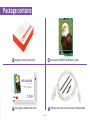
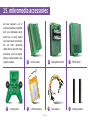
Package contains
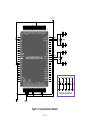
mikromedia for dsPIC33® - pinout
01 Damage resistant protective box
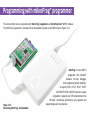
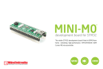
02 mikromedia for dsPIC33® development system
5V power supply
5V
RST
Reset pin
Reference Ground
GND
GND
Reference Ground
AN10
RB1
L
left ch.
audio out
AN2/SS1/CN4
RB2
R
right ch.
AN3/CN5
RB3
RD0
OC1
AN4/CN6
RB4
RD1
OC2
AN5/CN7
RB5
RD2
OC3
AN8
RB8
RD3
OC4
AN9
RB9
RD4
OC5/CN13
AN20/INT1
RA12
RD5
OC6/CN14
®
AN21/INT2
RA13
RD8
IC1
IC2
INT3
RA14
RD9
INT4
RA15
RD14
IC7/U1CTS/CN20
PGEC1/AN6/OCFA
RB6
RD15
IC8/U1RTS/CN21
PGED1/AN7
RB7
RD6
OC7/CN15
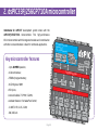
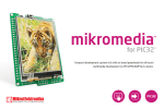
Compact development system rich with on-board peripherals
for
all-round
SCK1/INT0
RF6
RC2
AN17/T3CK/T6CK
SDI1
RF7
RF12
U2CTS
SPI1
multimedia development on dsPIC33FJ256GP710A
device.
SDO1
RF8
RF13
U2RTS
COFS
RG15
RF0
C1RX
CAN
C2RX
RG0
RF1
C1TX
RD10
IC3
RF2
U1RX
UART
RG6
SCK2/CN8
RF3
U1TX
SDI2/CN9
RG7
RG2
SCL1 I2C
SPI2
SDO2/CN10 We present
RG8
SDA1 ™ for dsPIC33®
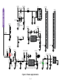
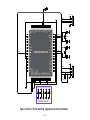
you with a complete color schematics forRG3
mikromedia
3.3V power supply
3.3V
3.3V
3.3V power supply
board. We want you to know what yourGND
board is
consisted
Reference Ground development
GND
Reference
Groundof and
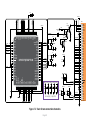
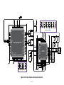
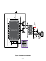
SCHEMATICS
mikromedia
for dsPIC33
mikromedia
™
™
for dsPIC33®
Pin functions
Programming lines
how it actually works.
Analog Lines
Interrupt Lines
Pin functions
SPI Lines
I2C Lines
UART lines
PWM lines
Comparator lines
03 User’s guide, schematic and pinout
04 USB cable, two 1x26, one 1x6 and one 1x5 male headers
Page 5