1
EPC®-1316
User’s Guide
www.radisys.com
World Headquarters
5445 NE Dawson Creek Drive • Hillsboro, OR 97124 USA
Phone: 503-615-1100 • Fax: 503-615-1121
Toll-Free: 800-950-0044
International Headquarters
Gebouw Flevopoort • Televisieweg 1A
NL-1322 AC • Almere, The Netherlands
Phone: 31 36 5365595 • Fax: 31 36 5365620
007-01065-0001
October 2001
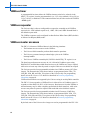
DANGER
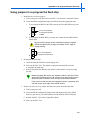
If you plan to connect a floppy drive, you must use a RadiSys EXP-FDM (Floppy Disk Module).
Connecting a standard floppy drive can create a fire hazard and may damage or destroy the
EPC-1316 baseboard, MSIO carrier board, MSF option board, EXP-FDM, or cable.
October 2001
Copyright ” 2001 by RadiSys Corporation
All rights reserved
EPC, INtime, iRMX, MultiPro, RadiSys, The Inside Advantage, and ValuPro are registered trademarks of
RadiSys Corporation. ASM, Brahma, DAI, DAQ, MultiPro, SAIB, Spirit, and ValuePro are trademarks of RadiSys
Corporation.
DAVID, MAUI, OS-9, and OS-9000, are registered trademarks of RadiSys Microware Communications
Software Division, Inc. FasTrak, Hawk, SoftStax, and UpLink are trademarks of RadiSys Microware
Communications Software Division, Inc.
†
All other trademarks, registered trademarks, service marks, and trade names are the property of their
respective owners.
Before you begin
This manual provides detailed hardware reference information for OEMs, system
integrators, and others who use the EPC-1316 as a component of their VMEbus systems.
It also explains how to install the EPC-1316, and configure the BIOS and the board
configuration options.
This manual assumes that you are familiar with both PC systems based on the Intel x86
architecture and with VMEbus architecture.
Guide contents
Chapters
Chapter
11 Overview
2
3
4
5
Description
Provides an introduction to the EPC-1316, a brief
description of the features provided, and
specifications.
Configuration and installation Covers the details of installing the EPC-1316 in a
VME mainframe.
BIOS configuration
Describes the process of BIOS configuration using the
built-in BIOS setup menus.
Theory of operation
Describes how the components of the EPC-1316
operate to provide a PCI/VMEbus compatible
embedded computer with standard PC peripherals
and PCI, and VME interfaces.
Programming the
Describes initializing and programming the VMEbus
VMEbus interface
interface using the system BIOS and the Tundra
Universe II† PCI-VME bridge chip.
Appendices
Appendix
A Chipset and I/O map
B
C
D
E
Description
Maps the addresses used for I/O and by the
chipset registers.
Interrupts
Shows the DMA channel and IRQ assignments to the
peripherals supported by the EPC-1316.
Connectors
Details the location, form, and pin-outs of the
connectors used in the EPC-1316.
Registers
Maps the address space used by EPC-1316 and
VMEbus registers.
Error messages and diagnosis Provides explanations of common error messages and
start-up codes.
iii
EPC-1316 User’s Guide
Appendix
F MSIO Carrier Board
G
H
I
J
K
L
Description
Describes how to configure and use the MSIO
option board.
MSF option board
Describes how to and use the MSF option board.
Flash disk module
Describes how to install, configure, and use the
optional Flash module.
PMC modules
Describes how to install, configure, and use optional
PMC modules.
Installing and configuring
Describes how to install, configure, and enable a
RomPilot
RomPilot image on a server and the Management
Workstation software on a client.
Re-programming the flash chip Explains how to update or recover your system BIOS,
Flash Boot Device (FBD), and Boot Block by
re-programming the Flash chip on the main board.
Glossary
Defines terms used in this guide.
Notational conventions
This manual uses the following conventions:
•
Screen text and syntax strings appear in this font.
•
All numbers are decimal unless otherwise stated.
•
Bit 0 is the low-order bit. If a bit is set to 1, the associated description is true unless
otherwise stated.
Notes indicate important information
about the product.
Tips indicate alternate techniques or
procedures that you can use to save
time or better understand the product.
The globe indicates a World Wide
Web address.
The book indicates a book or file.
ESD cautions indicate situations that
may cause damage to hardware via
electro-static discharge (ESD).
iv
Cautions indicate potentially
hazardous situations which, if not
avoided, may result in minor or
moderate injury, or damage to
data or hardware. It may also alert
you about unsafe practices.
Warnings indicate potentially
hazardous situations which, if not
avoided, can result in death or
serious injury.
Danger indicates imminently
hazardous situations which, if not
avoided, will result in death or
serious injury.
Before you begin
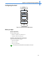
Where to get more information
About the EPC-1316
You can find out more about the EPC-1316 from these sources:
•
World Wide Web: RadiSys maintains an active site on the World Wide Web. The site
contains current information about the company and locations of sales offices, new
and existing products, contacts for sales, service, and technical support information.
You can also send e-mail to RadiSys using the web site.
When sending e-mail for technical support, please include information about
both the hardware and software, plus a detailed description of the problem,
including how to reproduce it.
To access the RadiSys web site, enter this URL in your web browser:
http://www.radisys.com
Requests for sales, service, and technical support information receive
prompt response.
•
Other: If you purchased your RadiSys product from a third-party vendor, you can
contact that vendor for service and support.
v
EPC-1316 User’s Guide
vi
Contents
Chapter 1: Overview
Feature summary..............................................................................................................................................
VMEbus ............................................................................................................................................................
System controller functions .......................................................................................................................
VMEbus master interface ..........................................................................................................................
VMEbus extended register set ...................................................................................................................
PCI Mezzanine card interface....................................................................................................................
Specifications....................................................................................................................................................
Environmental specifications.....................................................................................................................
Power supply requirement specifications ..................................................................................................
Additional specifications ..........................................................................................................................
3
4
4
4
4
4
5
5
5
5
Chapter 2: Configuration and installation
Configuring the EPC-1316 ...............................................................................................................................
Slot-1 functionality ....................................................................................................................................
Selecting the EPC-1316 slot location ........................................................................................................
Installing the VMEbus backplane jumper .................................................................................................
Setting jumpers on the backplane ..............................................................................................................
Setting jumpers on the boards ...................................................................................................................
MFG/Flash..........................................................................................................................................
Inserting the EPC-1316.....................................................................................................................................
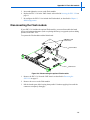
Maintaining and upgrading the EPC-1316 .......................................................................................................
Extracting the EPC-1316 ...........................................................................................................................
Dis-assembling the EPC-1316...................................................................................................................
Replacing the battery ................................................................................................................................
Upgrading main system memory...............................................................................................................
Installing other options ..............................................................................................................................
Re-assembling the EPC-1316 ....................................................................................................................
8
8
8
8
9
11
11
11
12
13
13
14
14
16
16
Chapter 3: BIOS configuration
BIOS setup screens ...........................................................................................................................................
Main menu .......................................................................................................................................................
Primary/Secondary Master/Slave sub-menus ............................................................................................
Keyboard Features sub-menu ....................................................................................................................
UBE Shadow Control sub-menu ...............................................................................................................
About shadow memory regions..........................................................................................................
Advanced Menu ................................................................................................................................................
PCI Configuration sub-menu.....................................................................................................................
PCI/PNP ISA UMB Region Exclusion sub-menu..............................................................................
PCI/PNP ISA IRQ Resource Exclusion sub-menu ............................................................................
Cache Memory sub-menu..........................................................................................................................
I/O Device Configuration sub-menu .........................................................................................................
Advanced Chipset Control sub-menu........................................................................................................
17
18
21
25
26
26
29
31
32
33
34
37
39
vii
EPC-1316 User’s Guide
Security menu ...................................................................................................................................................
Power menu ......................................................................................................................................................
Boot menu.........................................................................................................................................................
VME menu .......................................................................................................................................................
Exit menu ..........................................................................................................................................................
CMOS Save and Restore sub-menu ..........................................................................................................
40
41
43
44
46
48
Chapter 4: Theory of operation
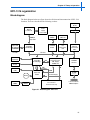
Overview...........................................................................................................................................................
EPC-1316 organization .....................................................................................................................................
Block diagram............................................................................................................................................
Features .............................................................................................................................................................
Processor....................................................................................................................................................
Cache memory ...........................................................................................................................................
Main system memory ................................................................................................................................
Memory map..............................................................................................................................................
PCI resources .............................................................................................................................................
Ethernet controller .....................................................................................................................................
Video controller .........................................................................................................................................
Flash boot device .......................................................................................................................................
BIOS ROM and ROM shadowing......................................................................................................
Keyboard/mouse controller .......................................................................................................................
CMOS backup and restore.........................................................................................................................
Battery........................................................................................................................................................
Watchdog timer..........................................................................................................................................
Peripheral ports..........................................................................................................................................
RS-232 ports.......................................................................................................................................
USB port.............................................................................................................................................
IDE ports ............................................................................................................................................
PCI/VME bridge........................................................................................................................................
Resetting the EPC-1316.............................................................................................................................
Power-off, power-on...........................................................................................................................
Power low...........................................................................................................................................
Front panel Reset button.....................................................................................................................
Ctrl+Alt+Del ......................................................................................................................................
VMEbus SYSRESET .........................................................................................................................
Watchdog timer...................................................................................................................................
Notes on byte ordering......................................................................................................................................
49
51
51
52
52
52
52
52
53
53
53
54
54
56
56
56
57
57
58
58
58
58
59
59
59
59
59
59
59
59
Chapter 5: Programming the VMEbus interface
Register initialization ........................................................................................................................................
Programming the Universe chip .......................................................................................................................
VMEbus arbiter.................................................................................................................................................
VMEbus timer...................................................................................................................................................
VMEbus requester ............................................................................................................................................
VMEbus master accesses..................................................................................................................................
VMEbus locked accesses (RMW) ....................................................................................................................
VMEbus interrupter ..........................................................................................................................................
VMEbus access to Universe registers...............................................................................................................
PCIbus access to Universe registers ................................................................................................................
For more programming information .................................................................................................................
viii
63
63
63
64
64
64
65
65
65
65
66
Contents
Appendix A: Chipset and I/O map
First (8-bit) DMA controller ............................................................................................................................
First interrupt controller....................................................................................................................................
Counter-timer functions ....................................................................................................................................
Keyboard controller and port ............................................................................................................................
Time-of-day clock.............................................................................................................................................
Phoenix NuBIOS ..............................................................................................................................................
DMA page registers: Intel EX 82371EB of PC/AT ..........................................................................................
Port A ................................................................................................................................................................
Second interrupt controller ...............................................................................................................................
Power management controller ..........................................................................................................................
Second (16-bit) DMA controller.......................................................................................................................
Coprocessor interface .......................................................................................................................................
IDE control .......................................................................................................................................................
ISA Plug and Play control ................................................................................................................................
Serial I/O (COM B) port ..................................................................................................................................
Parallel I/O (LPT1) port ....................................................................................................................................
EPP registers .....................................................................................................................................................
VGA..................................................................................................................................................................
Serial I/O (COM A) port...................................................................................................................................
First interrupt controller: Intel EX 82371EB of PC/AT....................................................................................
ISA Plug and Play.............................................................................................................................................
ISA Plug and Play.............................................................................................................................................
VME and miscellaneous registers ....................................................................................................................
ULA relative VXI registers within VME address space...................................................................................
67
67
67
68
68
68
68
69
69
69
69
70
70
70
70
71
71
71
72
72
72
72
72
73
Appendix B: Interrupts
Interrupts ...........................................................................................................................................................
DMA Channels .................................................................................................................................................
75
76
Appendix C: Connectors
Connector locations ..........................................................................................................................................
Ethernet .............................................................................................................................................................
Host PCI............................................................................................................................................................
Host peripheral .................................................................................................................................................
Keyboard...........................................................................................................................................................
Mouse................................................................................................................................................................
PMC .................................................................................................................................................................
RS-232 port (COM A) ......................................................................................................................................
SVGA (display monitor interface)....................................................................................................................
USB...................................................................................................................................................................
VMEbus P1.......................................................................................................................................................
VMEbus and interface P2 .................................................................................................................................
Reset switch ......................................................................................................................................................
77
79
80
82
83
83
84
86
86
86
87
88
89
Appendix D: Registers
Registers specific to the EPC-1316 ..................................................................................................................
Register details..................................................................................................................................................
Message registers (814Ch–814Fh) ...........................................................................................................
Control register (8150) .............................................................................................................................
ULA (8151h) .............................................................................................................................................
VME event register (8152h) ......................................................................................................................
91
92
92
93
93
93
ix
EPC-1316 User’s Guide
VME event enable register (8153h) ..........................................................................................................
Status/control register (8154h) .................................................................................................................
Status/control register (8155h) ..................................................................................................................
Model register (8156h) .............................................................................................................................
Signal FIFO low (8158h) ..........................................................................................................................
Signal FIFO high (8159h)..........................................................................................................................
Response register (815Ah) .......................................................................................................................
Response register (815Bh).........................................................................................................................
IRQ register (8161h) .................................................................................................................................
IACK latches (8162h–816Fh) ...................................................................................................................
VXI register details ...........................................................................................................................................
ID/ULA register (offset 0h) ......................................................................................................................
ID/ULA register (offset 1h) .......................................................................................................................
Device type register (offset 2h) ................................................................................................................
Device type register (offset 3h) .................................................................................................................
Status/control register (offset 4h) .............................................................................................................
Status/control register (offset 5h) ..............................................................................................................
Protocol low register (offset 8h) ...............................................................................................................
Protocol high register (offset 9h) ...............................................................................................................
Response register (offset Ah) ...................................................................................................................
Response register (offset Bh) ....................................................................................................................
Message high register (offset Ch) .............................................................................................................
Message high register (offset Dh)..............................................................................................................
Message low register (offset Eh ................................................................................................................
Message low register (offset Fh) ...............................................................................................................
VXI register base address decoding..................................................................................................................
94
94
94
94
95
95
95
95
95
96
96
96
96
97
97
97
97
98
98
98
98
100
100
100
100
100
Appendix E: Error messages and diagnosis
Boot failures...................................................................................................................................................... 101
Troubleshooting ................................................................................................................................................ 102
Appendix F: MSIO Carrier Board
Overview...........................................................................................................................................................
Configuration ....................................................................................................................................................
Setting Jumpers on the MSIO Carrier Board ............................................................................................
COM B configuration.........................................................................................................................
SCSI termination ................................................................................................................................
Disconnecting the MSIO Carrier Board ....................................................................................................
Re-assembling the MSIO Carrier Board and the Main board ...................................................................
BIOS configuration...........................................................................................................................................
Organization......................................................................................................................................................
Block diagram............................................................................................................................................
Feature set..................................................................................................................................................
SCSI interface.....................................................................................................................................
Peripheral ports...................................................................................................................................
COM B ports ......................................................................................................................................
Parallel port ........................................................................................................................................
Floppy controller ................................................................................................................................
Connectors ........................................................................................................................................................
Connector locations ...................................................................................................................................
EIDE (primary)..........................................................................................................................................
x
103
104
105
105
105
106
107
107
108
108
108
108
108
109
109
109
109
109
111
Contents
EXP-FDM floppy ......................................................................................................................................
Parallel port................................................................................................................................................
RS-232/RS-485 port (COM B)..................................................................................................................
SCSI-2 .......................................................................................................................................................
112
112
113
114
Appendix G: MSF option board
Overview...........................................................................................................................................................
Specifications....................................................................................................................................................
Environmental specifications.....................................................................................................................
Configuration ....................................................................................................................................................
Setting Jumpers on the MSF option board ...............................................................................................
COM B configuration.........................................................................................................................
Disconnecting the MSF option board ........................................................................................................
Re-assembling the MSF option board and the Main board .......................................................................
BIOS configuration...........................................................................................................................................
Organization......................................................................................................................................................
Block diagram............................................................................................................................................
Feature set..................................................................................................................................................
COM B ports ......................................................................................................................................
Parallel port ........................................................................................................................................
Serial port interface (COM3 through COM6) ....................................................................................
PC-compatible parallel interface ........................................................................................................
Hard drive, Compact Flash drive, and floppy drive ..................................................................................
Hard drive interface............................................................................................................................
Compact Flash drive interface............................................................................................................
Floppy disk Interface..........................................................................................................................
UART-to-PCI bridge .................................................................................................................................
Ethernet controller .....................................................................................................................................
Connectors ........................................................................................................................................................
Connector locations ...................................................................................................................................
Compact Flash header................................................................................................................................
EIDE (primary)..........................................................................................................................................
Ethernet......................................................................................................................................................
EXP-FDM floppy ......................................................................................................................................
Parallel port................................................................................................................................................
RS-232/RS-485 port (COM B)..................................................................................................................
115
116
116
117
118
118
119
120
120
121
121
121
121
121
122
122
122
122
122
122
122
122
123
123
124
125
126
127
128
128
Appendix H: Flash disk module
Installing the Flash module...............................................................................................................................
Installing the CompactFlash card on the Flash module.............................................................................
Installing the Flash module on the Main board .........................................................................................
Disconnecting the Flash module.......................................................................................................................
Organization......................................................................................................................................................
Block diagram............................................................................................................................................
Feature set..................................................................................................................................................
Specifications.............................................................................................................................................
Connectors ........................................................................................................................................................
Floppy disk drive (optional) ......................................................................................................................
Host peripheral ..........................................................................................................................................
Host PCI ...................................................................................................................................................
129
129
129
131
132
132
132
133
134
134
135
137
xi
EPC-1316 User’s Guide
Appendix I: PMC modules
Installing a PMC module on the Main board.................................................................................................... 139
Disconnecting the PMC module ....................................................................................................................... 140
Appendix J: Installing and configuring RomPilot
About RomPilot ................................................................................................................................................
Configuring and enabling the RomPilot image ................................................................................................
Before you begin........................................................................................................................................
Configure RomPilot...................................................................................................................................
Network and driver information.........................................................................................................
Server information..............................................................................................................................
Enable RomPilot........................................................................................................................................
Configuring the client .......................................................................................................................................
Before you begin........................................................................................................................................
System requirements ..........................................................................................................................
Installation and configuration requirements.......................................................................................
Install and set up MWA software...............................................................................................................
Install MWA .......................................................................................................................................
Set up MWA to communicate with servers ........................................................................................
Link the client with server(s).....................................................................................................................
144
144
145
145
146
147
148
149
149
149
149
150
150
150
150
Appendix K: Re-programming the flash chip
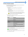
About the flash chip ..........................................................................................................................................
About re-programming the flash chip...............................................................................................................
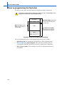
Before you begin...............................................................................................................................................
Creating a Flash Boot diskette ..........................................................................................................................
Using phlash.exe to re-program the flash chip .................................................................................................
Using BIOS configuration options to re-program the flash chip......................................................................
Using jumpers to re-program the flash chip .....................................................................................................
151
152
153
155
157
158
159
Appendix L: Glossary ...................................................................................................................................... 161
Index ...................................................................................................................................................................... 169
xii
Contents
Figures
Figure 1-1. The EPC-1316, shown with no options.................................................................................................
Figure 2-1. Daisy-chain signal concept....................................................................................................................
Figure 2-2. VMEbus jumpers on rear wirewrap pins...............................................................................................
Figure 2-3. VMEbus jumpers on front stake pins ....................................................................................................
Figure 2-4. EPC-1316 assembly: jumper locations .................................................................................................
Figure 2-5. Flash jumper settings.............................................................................................................................
Figure 2-6. Inserting SODIMMs..............................................................................................................................
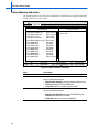
Figure 3-1. Main menu.............................................................................................................................................
Figure 3-2. Master/Slave sub-menu .........................................................................................................................
Figure 3-3. Keyboard Features sub-menu................................................................................................................
Figure 3-4. UBE Shadow Control sub-menu ...........................................................................................................
Figure 3-5. Advanced menu.....................................................................................................................................
Figure 3-6. PCI Configuration sub-menu ................................................................................................................
Figure 3-7. PCI/PNP ISA UMB Region Exclusion sub-menu ................................................................................
Figure 3-8. PCI/PNP ISA IRQ Resource Exclusion sub-menu ...............................................................................
Figure 3-9. Cache memory sub-menu......................................................................................................................
Figure 3-10. I/O Device Configuration sub-menu ...................................................................................................
Figure 3-11. Advanced Chipset Control sub-menu..................................................................................................
Figure 3-12. Security menu......................................................................................................................................
Figure 3-13. Power menu.........................................................................................................................................
Figure 3-14. Boot menu ...........................................................................................................................................
Figure 3-15. VME menu ..........................................................................................................................................
Figure 3-16. Exit menu ............................................................................................................................................
Figure 3-17. CMOS Save and Restore sub-menu ....................................................................................................
Figure 4-1. Block diagram: EPC-1316 ....................................................................................................................
Figure 4-2. Flash boot device memory: upper 512 KB............................................................................................
Figure 4-3. Flash boot device memory: lower 512 KB............................................................................................
Figure 4-4. Using big-endian byte ordering.............................................................................................................
Figure C-1. EPC-1316 assembly: main board connectors .......................................................................................
Figure F-1. EPC-1316 with MSIO Carrier Board....................................................................................................
Figure F-2. MSIO Carrier BoardMSIO Carrier Board assembly: jumper locations................................................
Figure F-3. COM B jumper settings ........................................................................................................................
Figure F-4. SCSI jumper settings.............................................................................................................................
Figure F-5. Disconnecting the optional MSIO Carrier Board .................................................................................
Figure F-6. Attaching the MSIO Carrier Board to the Main board .........................................................................
Figure F-7. Block diagram: MSIO Carrier Board....................................................................................................
Figure F-8. MSIO Carrier Board: connectors ..........................................................................................................
Figure G-1. EPC-1316 with MSF option board .......................................................................................................
Figure G-2. MSF option board assembly: jumper locations ....................................................................................
Figure G-3. COM B jumper settings........................................................................................................................
Figure G-4. Disconnecting the MSF option board...................................................................................................
Figure G-5. Attaching the MSF option board to the Main board ............................................................................
Figure G-6. Block diagram: MSF option board.......................................................................................................
Figure G-7. MSF option board: connectors .............................................................................................................
Figure H-1. Installing the CompactFlash card on the Flash module .......................................................................
Figure H-2. Installing the optional Flash module on the EPC-1316........................................................................
Figure H-3. Disconnecting the optional Flash module ............................................................................................
Figure H-4. Block diagram: Flash module...............................................................................................................
1
9
10
10
11
11
15
18
21
25
27
29
31
32
33
34
37
39
40
41
43
44
46
48
51
55
56
61
78
103
105
105
105
106
107
108
110
116
118
118
119
120
121
124
129
130
131
132
xiii
EPC-1316 User’s Guide
Figure H-5. Flash module dimensions .....................................................................................................................
Figure H-6. Flash module connectors ......................................................................................................................
Figure I-1. Inserting a PMC module ........................................................................................................................
Figure I-2. Disconnecting an optional PMC module ...............................................................................................
Figure J-1. Where RomPilot components reside .....................................................................................................
Figure J-2. Configuring and enabling RomPilot......................................................................................................
Figure J-3. RomPilot Main menu.............................................................................................................................
Figure J-4. Installing RomPilot’s MWA software....................................................................................................
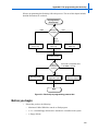
Figure K-1. Flash chip configuration .......................................................................................................................
Figure K-2. Flash chip re-programming coverage...................................................................................................
Figure K-3. Flash chip re-programming process flow .............................................................................................
xiv
133
134
139
141
143
145
146
149
151
152
153
Contents
Tables
Table 1-1. EPC-1316 environmental specifications.................................................................................................
Table 1-2. EPC-1316 power supply specifications ..................................................................................................
Table 1-3. Additional EPC-1316 specifications.......................................................................................................
Table 3-1. BIOS Setup menu map............................................................................................................................
Table 4-1. EPC-1316 device ~IDSEL assignments .................................................................................................
Table B-1. Interrupts ................................................................................................................................................
Table B-2. DMA channels........................................................................................................................................
Table C-1. RJ45 phone jack pin-out.........................................................................................................................
Table C-2. Host PCI connector ................................................................................................................................
Table C-3. Host PCI connector power pins..............................................................................................................
Table C-4. Host peripheral connector ......................................................................................................................
Table C-5. Host peripheral connector power pins....................................................................................................
Table C-6. Keyboard pin-out....................................................................................................................................
Table C-7. Mouse pin-out ........................................................................................................................................
Table C-8. PMC 1 connector pin-out .......................................................................................................................
Table C-9. PMC 2 connector pin-out .......................................................................................................................
Table C-10. DB-9 pin-out ........................................................................................................................................
Table C-11. DB-15 pin-out.......................................................................................................................................
Table C-12. USB connector .....................................................................................................................................
Table C-13. VMEbus P1 connector pin-out.............................................................................................................
Table C-14. VMEbus P2 connector pin-out.............................................................................................................
Table E-1. Troubleshooting error messages .............................................................................................................
Table F-1. Primary EIDE connector ........................................................................................................................
Table F-2. EXP-FDM floppy connector ..................................................................................................................
Table F-3. DB-25 pin-out ........................................................................................................................................
Table F-4. RS-232 pin-out........................................................................................................................................
Table F-5. RS-485 pin-out........................................................................................................................................
Table F-6. SCSI-2 connector ...................................................................................................................................
Table 5-1. EPC-1316 environmental specifications.................................................................................................
Table E-1. Compact Flash header ............................................................................................................................
Table G-1. Primary EIDE connector .......................................................................................................................
Table G-2. RJ45 phone jack pin-out ........................................................................................................................
Table G-3. EXP-FDM floppy connector .................................................................................................................
Table G-4. DB-25 pin-out .......................................................................................................................................
Table G-5. RS-232 pin-out.......................................................................................................................................
Table G-6. RS-485 pin-out.......................................................................................................................................
Table H-1. Flash module environmental specifications...........................................................................................
Table H-2. Flash module power supply specifications ............................................................................................
Table H-3. Standard floppy pin-out .........................................................................................................................
Table H-4. Host peripheral connector ......................................................................................................................
Table H-5. Host peripheral connector power pins ..................................................................................................
Table H-6. Host PCI connector ................................................................................................................................
Table H-7. Host PCI connector power pins ............................................................................................................
5
5
5
17
53
75
76
79
80
81
82
83
83
83
84
85
86
86
86
87
88
102
111
112
112
113
113
114
116
124
125
126
127
128
128
128
133
133
134
135
136
137
138
xv
EPC-1316 User’s Guide
xvi
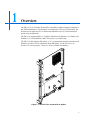
Overview
Chapter 1
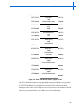
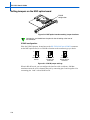
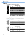
The EPC®-1316 is a Pentium† III-based PC-compatible computer designed to interface to
the VME backplane bus. The electronics are comprised of a 6U size I/O base board. The
board comes in single-slot (6U I/O baseboard) and double-slot (6U I/O baseboard plus
option card) configurations.
The EPC-1316 supports DOS 6.22, VxWorks, and Microsoft† Windows† 95, Windows 98,
Windows NT† V4 and Windows 2000. The system is year-2000 ready.
The EPC-1316 also supports EPConnect, a C/C++ programming interface to the Microsoft
Windows NT API. For more information about EPConnect, see the EPConnect for
Windows NT/4.0 Programmer’s Reference Guide, available from Radisys.
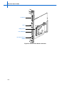
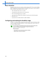
Figure 1-1. The EPC-1316, shown with no options
1
EPC-1316 User’s Guide
The EPC-1316 can be ordered in these configurations:
Configuration
EPC-1316
EPC-1316 +
MSIO Carrier
Board1
Options
Description
You can order this The Flash disk module is a 64-Mbyte PCI
configuration with: Mezzanine card that conforms to IEEE P1386.1.
Available only for EPC-1316s that do not include
• No options.
an option card or PMC card.
• A Flash disk
For more information about PMC modules, see
module.
Appendix I, PMC modules.
You can order this The EPC-1316 board plus a mass storage and I/O
configuration with: expansion board (MSIO) which provides SCSI,
LPT, floppy drive, and IDE (primary) interfaces, as
• A hard disk
well as one RS-232/RS-485 serial port.
drive.
For more information about the Carrier board, see
Appendix F, MSIO Carrier Board.
You can order this The EPC-1316 board plus an MSF (Multi-Serial
configuration with: Feature) card that provides secondary storage and
multiple I/O functions.
• A hard disk
drive.
For more information about the Carrier board, see
Appendix G, MSF option board.
• A Flash drive.
• A Flash drive.
EPC-1316 +
MSF option
board1
1
Available only for EPC-1316 boards not fitted with the Flash disk module option.
The EPC-1316 can be fitted with a PMC module, a PCI Mezzanine card that conforms to
IEEE P1386.1. Available only for EPC-1316s that do not include the Flash disk module.
For more information about PMC modules, see Appendix I, PMC modules.
The EPC-1316 does not require a RadiSys-manufactured PMC. The EPC-1316
can accept most PMC types excluding those that either require a disk BIOS in the
EPC or do not fit by form factor.
2
Chapter 1: Overview
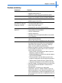
Feature summary
Component
Processor
Features
• BGA2 processor.
• 400 MHz mobile Pentium III.
Main memory
• 256KB of L2 cache, running at full processor speed.
• Two 144-pin PC100 SODIMM sockets.
Intel North Bridge 443BX
• Supports up to 256 MB synchronous DRAM (SDRAM).
• Host Bus to 32 bit, 33 MHz PCI bridge.
Intel South Bridge
82371EB PCI ISA IDE
Xcelerator (PIIX4E)
• SDRAM support without ECC.
• PCI to ISA bridge.
• Two independent EIDE channels.
• Single channel USB support.
• Integrated RTC with external battery backup.
National PC87309-ICK-VLJ • Two serial ports (one provided by MSIO).
Super I/O
• One parallel port (only with MSIO).
• One PS/2 keyboard port.
• One PS/2 mouse port.
Video graphics
• Two floppy drives (one supported by MSIO, one provided
via P2 connector).
• Chips and Technology 69030 64-bit GUI and
video-accelerated controller.
• 4 MB of video memory integrated into the video controller.
Other features
• Phoenix†-based PC BIOS with Flash update capability
from floppy. Writes to the BIOS Flash are controlled by
software that uses registers in the chipset. Installing a
jumper can force updates to the BIOS Flash.
• Remote management capability, using RomPilot software.
• Full 32-bit VME bus interface with P1 and P2 connectors
which includes these features:
• Master control in the A16/A24/A32 address spaces for
D08, D16, and D32 data widths.
• D64/D32/D16/D08 slave control in the A32/A24 address
space for dual port DRAM.
• D16 slave control in the A16 address space for dualported VXI configuration and message-passing registers.
• VME-bus arbiter, SYSCLOCK driver, and bus time-out.
• Generate and respond to all seven VME-bus interrupts.
• One IEEE P1386.1 PCI Mezzanine Card site via front panel.
• PCI-based Ethernet 10/100 BASE-T interface with an
RJ45 connector.
• Watchdog timer. This device can, upon proper
configuration, generate a VMEbus SYSFAIL signal and
either halt or perform a warm reboot of the processor. The
timer is implemented as a software-retriggerable one-shot,
with a programmable reset interval ranging from 128 ms to
8.2 seconds.
3
EPC-1316 User’s Guide
VMEbus
The Universe† chip (the Tundra† Universe II VME/PCI Bridge chip with enhancements
for multiprocessor environments) controls the VMEbus. The next sections cover system
controller functions, the VMEbus master interface, and the VMEbus extended register set.
System controller functions
The Universe chip allows the EPC-1316 to provide full VME Slot-1 arbitration functions.
When enabled, these functions include priority and round-robin bus arbitration, IACK and
bus grant daisy-chain driving, SYSRESET and SYSCLK generation and bus time-out
detection. ROR (release-on-request), RWD (release when done) or a fair-requester, RONR
(release-on-no-request) bus release mechanism is software selectable.
VMEbus master interface
The VMEbus master interface provides a full 64/32-bit data path to the 16-, 24-, and 32-bit
address spaces of the VMEbus. The bus interface is designed with a minimum number of
state registers, which maximizes performance in a multitasking or
interrupt-driven environment.
Programmable hardware byte-swapping provides ease of communication with other
processor architectures that may share the VMEbus. All the VMEbus address spaces can
be addressed from both protected-mode and real-mode operating systems.
The EPC-1316 can generate or respond to all seven standard VMEbus interrupts, and can
also receive as interrupts the VMEbus signals ACFAIL, BERR, and SYSFAIL. When it
generates interrupts, the EPC-1316 implements 16-bit IACK cycles.
VMEbus extended register set
As an extension to the VMEbus interface, the EPC-1316 implements the set of VXIbus
(IEEE 1155-1992) standard multiprocessor support registers in the A16 space.
These registers provide a set of standard identification, status, control and communication
functions that are useful in multiprocessor environments. They allow dynamic system
configuration by providing for board identification, and provide well-defined
multi-processor communications channels and protocols.
The EPC-1316 includes a complete set of VXIbus-defined message-based device registers.
These registers are implemented in a proprietary gate array and mapped into the VMEbus
A16 address space and include a device-type identifier register, bus status and control
registers, and a register-based message passing facility.
PCI Mezzanine card interface
The PMC card interface, which resides on the PCI bus as device 3 (AD14), has interrupt
and bus master capability.
The signal connections are for a 32-bit PCI revision 2.1 compliant interface and do not
have the 64-bit data path connector.
There is no provision for additional I/O signals via the PMC connectors.
For information about inserting PMC cards in this interface, see Appendix I, PMC modules.
4
Chapter 1: Overview
Specifications
Environmental specifications
Table 1-1. EPC-1316 environmental specifications
Characteristic
Temperature
Humidity
Altitude
Vibration
(excluding hard
drive)
Shock (excluding
hardd drive)
State
Operating
Storage
Operating
Storage
Operating
Storage
Operating
Storage
Operating
Storage
Airflow
Value
0 to 55°C at point of entry of forced air derated
2°C per 1000 ft. (300 m) over 6600 ft. (2000 m)
–40°C +85°C
5% to 95% noncondensing
5% to 95% noncondensing
0–10,000 ft (3000 m)
0–40,000 ft (12,000 m)
2.5 g acceleration over 5–300 Hz sine wave (P-P),
1 oct/min sine sweep
5 g acceleration over 5–2 kHz sine wave (P-P),
1 oct/min sine sweep
30 g, 11 ms duration, half-sine shock pulse
50 g, 11 ms duration, half-sine shock pulse
200 LFM (linear feet per minute)
Power supply requirement specifications
Table 1-2. EPC-1316 power supply specifications
Characteristic
Current
Value
+5V @ 4–7A (options excluded)
+12V @ 350 mA (options excluded)
–12V @ 50 mA (options excluded)
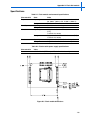
Additional specifications
Table 1-3. Additional EPC-1316 specifications
Characteristic
Mechanical
Weight
Dimensions
Safety
EMC
Value
Standard VME 6U card
2.7 lb. (1.3 kg) with PMC site unpopulated
One-slot 6U VMEbus model
UL 1950 73/23/EECLow-Voltage Directive using EN 60950
RadiSys embedded computers are designed with good EMC practices
as intended in “The Council of The European Communities EMC
Compatibility Directive” (89/336/EEC). RadiSys currently follows these
standards:
EN55022
EN55024
Limits and Methods, ITE
Immunity, ITE (where applicable)
5
EPC-1316 User’s Guide
Table 1-3. Additional EPC-1316 specifications
Characteristic
VME
Value
Master address
Master transfer
Slave address
Slave transfer
Interrupter
Interrupt handler
Requester
Arbiter
System controller
VXI
Device type
Protocols
Manufacturer code
Model code
A16, A24, A32
D08(EO), D16, D32, D64, RMW
A16
D08(EO), D16, RMW
I(1–7)
D08(O),D16 IH(1–7)
ROR, RONR, RWD
RRS, PRI
SYSCLK, IACK and bus grant daisy chain
drivers, and bus time-out error (BERR)
Message based
Servant/commander/master/interrupter
4076 RadiSys Corporation
101Fh (if configured for slot 0)
111Fh (if configured for other than slot 0)
6
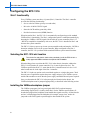
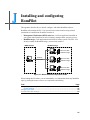
Configuration and installation
Chapter 2
This chapter explains how to install and configure the EPC-1316. To install or configure
options for the EPC-1316, see the appropriate appendix:
•
MSIO Carrier Board: see Appendix F, MSIO Carrier Board.
•
MSF option board: see Appendix G, MSF option board.
•
Flash disk module: see Appendix H, Flash disk module.
•
PMC modules: see Appendix I, PMC modules.
When reading this file online, you can immediately view information about any
installation topic by placing the mouse cursor over a connector name and clicking:
Task
Page
Configuring the EPC-1316.................................................................................................. 8
Slot-1 functionality........................................................................................................8
Selecting the EPC-1316 slot location........................................................................... 8
Installing the VMEbus backplane jumper ..................................................................... 8
Setting jumpers on the backplane ................................................................................ 9
Setting jumpers on the boards ...................................................................................11
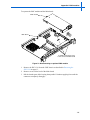
Inserting the EPC-1316 ....................................................................................................11
Maintaining and upgrading the EPC-1316........................................................................12
Extracting the EPC-1316............................................................................................13
Dis-assembling the EPC-1316 ...................................................................................13
Replacing the battery .................................................................................................14
Upgrading main system memory ...............................................................................14
Installing other options ...............................................................................................16
Re-assembling the EPC-1316....................................................................................16
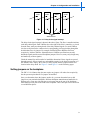
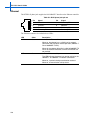
Avoid causing ESD damage:
• Remove modules from their antistatic bags only in a static-free environment.
• Perform the installation process (described later in this chapter) only in a
static-free environment.
• During the installation process, ensure that power to your system is off. The
EPC-1316 is not designed to be inserted or removed while the chassis is
powered up.
• During external cable installation, ensure that the cables are not active. The
EPC-1316 is not designed for hot insertion of any interface.
The EPC-1316 modules, like most other electronic devices, are susceptible to
electrostatic discharge (ESD) damage. ESD damage is not always immediately
obvious. It can cause a partial breakdown in semiconductor devices that might not
result in immediate failure.
7
EPC-1316 User’s Guide
Configuring the EPC-1316
Slot-1 functionality
Every VMEbus system must have a System (Slot-1) Controller. The Slot-1 controller
provides the following functionality:
•
Serves as the bus arbiter (priority or round-robin)
•
Drives the 16 MHz SYSCLK signal
•
Starts the IACK and bus grant daisy chain
•
Provides bus timeout error (BERR) function
When inserted in Slot 1, the EPC-1316 is automatically configured to provide standard
VMEbus Slot-1 functionality. The Slot-1 configuration option is enabled automatically by
detecting the VMEbus ~BG3IN signal if the board is the system controller (Slot-1). If
~BG3IN is sampled low immediately after reset, the EPC-1316 is installed in Slot-1 and
becomes the system controller.
The EPC-1316 always powers up in non-system controller mode and samples ~BG3IN to
determine whether or not it is the system controller. When configured as the Slot-1
controller, the EPC-1316 performs all the standard VMEbus system control functions.
Selecting the EPC-1316 slot location
To maintain fire and electric shock safety standards, install the EPC-1316 in a
safety-approved VMEbus enclosure compliant with EN-60950.
When deciding where to position the EPC-1316 in the chassis, determine whether the
EPC-1316 will function as system controller. If so, it must be placed in slot 1. The
VMEbus specification, Rule 3.3, states that the Slot-1 controller must be in slot 1. All
other boards must be to the right of the Slot-1 controller.
The EPC-1316 plus any option can be considered together as a single subsystem. Check
the total power requirements against the power supply ratings of your VMEbus system
and the other modules to ensure that the power supply can handle the total power required.
Once you determine the EPC-1316 subsystem physical location in the chassis, the
VMEbus backplane must be jumpered appropriately, as described in the following section.
Installing the VMEbus backplane jumper
The VMEbus propagates four bus grant signals (BG0–BG3) and one interrupt
acknowledge signal (IACK) via daisy-chain lines. Per the VMEbus specifications, all
boards (that plug into the backplane) must handle these signals correctly. All slots that do
not have a board plugged into the backplane (for example, empty slots), need to be
jumpered to allow the signals to pass through to other boards in the system.
8
Chapter 2: Configuration and installation
xxxIN
xxxIN
xxxIN
xxxIN
xxxOUT
xxxOUT
xxxOUT
xxxOUT
VMEbus Slots
Figure 2-1. Daisy-chain signal concept
The daisy-chain signal concept is shown in the above figure. The Slot-1 controller initiates
each daisy-chain signal. Each VMEbus slot to the right of the Slot-1 controller, as viewed
from the front, must pass through each of the daisy-chained signals. For each VMEbus
slot, the xxxIn pin must be connected to its corresponding xxxOut pin either through the
board in that slot or by jumper. For example, BG0In–BG3In to BG0Out–BG3Out,
respectively; IackIn to IackOut. (Boards that meet VMEbus specifications correctly
handle the signals and do not need backplane jumpers. However, many early designs may
not handle any of these signals.)
Check the manual for each board to be installed to determine if these signals are passed
through correctly. If these signals are not handled correctly by the board in question or if
the VMEbus slot is empty, all (or some) of these signals must be jumpered to the next
location in the daisy-chain. See Figure 2-2 and Figure 2-3 on the following pages.
Setting jumpers on the backplane
The EPC-1316’s leftmost slot does not require any jumpers. All other slots occupied by
the subsystem require that all five jumpers be installed.
Once you determine where the jumpers need to be, you must determine how to add
jumpers to your particular backplane. Different backplane manufacturers handle this in
different ways: some provide stake pins or wirewrap pins on the rear of the backplane
while others provide pins on the front of the backplane. These stake pins can be located in
several different places.
9
EPC-1316 User’s Guide
J1 Connector
BG0
BG1
BG2
BG3
IACK
Figure 2-2. VMEbus jumpers on rear wirewrap pins
If the stake pins are on the rear of the backplane, the most common location is in the
middle of the J1 connector as shown in Figure 2-2. The connector may have wire-wrap
tails on all pins, or just on the bus-grant and IACK pins.
Stake pins (front or rear) can also be located adjacent to the slot being jumpered as shown
in Figure 2-3. Typically, the stake pins are located between the jumpered slot and the next
lower-numbered slot (for example, jumpers for Slot 6 are located adjacent to Slot 6,
between Slots 5 and 6).
J1 Connectors
BG0
BG1
BG2
BG3
IACK
Figure 2-3. VMEbus jumpers on front stake pins
Consult your VMEbus chassis reference manual or contact the chassis manufacturer if you
are unsure where to jumper your particular system.
10
Chapter 2: Configuration and installation
Setting jumpers on the boards
MFG/Flash
Figure 2-4. EPC-1316 assembly: jumper locations
Jumper pins are labeled from the point of view of looking at the front of
the connector.
MFG/Flash
The EPC-1316 provides a 2x6-pin header used for for testing purposes and to re-program
the Flash chip. For detailed information about re-programming the flash chip, see
Appendix K, Re-programming the flash chip.
Flash jumper settings are typically used during manufacturing for configuration and are
included here only for reference.
1
2
1
2
1
2
1
2
9
10
9
10
9
10
9
10
Pins 1 and 2:
Hardware reset
Pins 4-6:
Write Boot Block
Pins 3-5:
Force flash recovery
Pins 9-10:
Loop BIOS
Figure 2-5. Flash jumper settings
Inserting the EPC-1316
You install the EPC-1316 on the VMEbus backplane. Before installation, ensure that all
options are installed on the EPC-1316 as described in Maintaining and upgrading the
EPC-1316 later in this chapter.
11
EPC-1316 User’s Guide
1. Ensure that power to your VME system is off.
The EPC-1316 module is not designed to be inserted or removed from
“live” backplanes.
When handling or inserting the EPC-1316 module, avoid touching the circuit
board and connector pins, and ensure that the environment is static-free.
2. Ensure that the ejector handles are in the normal (non-eject) position. (Push the top
handle down and the bottom handle up so that the handles are not tilted.)
3. Slide the EPC-1316 module into the slot. Use firm pressure on the handles to mate the
module with the connectors.
4. Tighten the retaining screws in the top and bottom of the front panel to ensure proper
connector mating and to prevent the module from loosening due to vibration.
5. Connect peripherals to the EPC-1316. Periperals typically include a video display and
keyboard, but also perhaps a mouse, modem, printer, and so on. For information about
front-panel connector pinouts, see Appendix C, Connectors.
Observe the following while the system is powered up:
• Do not plug cables or connectors into the front panel connectors. Because
electronics equipment generally cannot withstand fluctuations in power,
damage can arise from plugging in a device or board while power is on.
• Do not plug in a serial or parallel device, keyboard, transceiver, monitor
or other component. This applies to equipment at either end of an
interface cable.
6. Complete remaining steps as required. Typical remaining steps include:
•
BIOS configuration (For information about setting up the BIOS configuration, see
Chapter 3, BIOS configuration.)
•
Driver software installation
•
Application software installation
Your system may be preconfigured by your supplier or you may be required to
perform these tasks yourself.
Maintaining and upgrading the EPC-1316
Occasionally you will want to perform maintenance (such as replacing the battery) or
upgrades (such as adding options) on the EPC-1316. When this occurs, you must extract
the board from the VME chassis, repair or install the desired option, then re-install the
board in the VME chassis.
If your EPC-1316 includes an option, you may need to disassemble the boards before
upgrades or maintenance, then re-assemble the boards before re-inserting the EPC-1316
into the VME chassis. The following sections describe how.
12
Chapter 2: Configuration and installation
Extracting the EPC-1316
Before performing certain maintenance operations such as replacing the battery or
upgrading memory, you must remove the EPC-1316 from the VME chassis:
1. Make sure that power to your VME system is off.
The EPC-1316 module is not designed to be inserted or removed from
“live” backplanes.
When handling or inserting the EPC-1316 module, avoid touching the circuit
board and connector pins, and ensure that the environment is static-free.
2. Loosen the retaining screws in the top and bottom of the front panel to prepare for
connector release.
3. Move the ejector handles to the eject position: push the top handle up and the bottom
handle down so that the handles appear tilted.
4. Slide the EPC-1316 module out of its slot. Pull firmly on the handles to release the
module from the connectors.
5. If your EPC-1316 includes an option, disassemble the board as described in
Dis-assembling the EPC-1316.
Dis-assembling the EPC-1316
To separate an option board from the main board:
1. Remove the EPC-1316 in the VME chassis as described in Extracting the EPC-1316.
2. Remove the option as described below:
•
MSIO Carrier Board: see Disconnecting the MSIO Carrier Board in Appendix
F, MSIO Carrier Board.
•
MSF option board: see Disconnecting the MSF option board in Appendix G,
MSF option board.
•
Flash disk module: see Disconnecting the Flash module in Appendix H, Flash
disk module.
•
PMC modules: see Disconnecting the Flash module in Appendix I, PMC
modules.
13
EPC-1316 User’s Guide
Replacing the battery
To replace the battery:
Perform these steps only in a static-free environment.
1. Before you begin, write down all the CMOS setup parameters while the battery is still
good, or save them using the CMOS save and restore feature of the BIOS
configuration Exit menu on page 46.
2. Turn off the power.
If you leave the power on when removing the battery, setup values return to
default conditions.
3. Remove the EPC-1316 from the VME chassis as described in Extracting the
EPC-1316.
4. Locate the battery on the main board (see Figure C-1), then lift the battery out.
Battery
5. Press the new battery into place, positive (+) side up.
There is danger of explosion if battery is incorrectly replaced. Replace only
with same or equivalent type recommended by RadiSys. Dispose of used
batteries according to manufacturer’s instructions.
6. If your EPC-1316 includes an option, re-assemble the board as described in
Re-assembling the EPC-1316.
7. Replace the EPC-1316 in the VME chassis as described in Inserting the EPC-1316.
8. Restore the CMOS settings as described in the CMOS Save and Restore sub-menu on
page 48.
After removing the old battery, you can ship it to this address for disposal:
CPD Division Material Disposal
Program Management
c/o RadiSys Corporation
5445 NE Dawson Creek Drive
Hillsboro, OR USA 97124
Upgrading main system memory
Main memory is implemented as SODIMM 144-pin socketed 3.3 volts SDRAM. The
main memory controller supports up to 256MB of PC100 SDRAM in two 144-pin
SODIMM sockets.
14
Chapter 2: Configuration and installation
It is best to populate the furthest SDRAM socket to reduce reflections. The first bank is
labeled BANK1 on the silkscreen.
To add memory:
Perform these steps only in a static-free environment.
1. Obtain DRAM modules. At the time of writing, the following sizes of PC100
SDRAM were useable:
Type
Row/column
Total Size (MB)
4Mx64
12/10, 14/8
32
8Mx64
12/11, 14/9, 14/8
64
16Mx64
12/12, 14/10
128
Row and column numbers identify the DRAM configuration on the
SODIMM modules.
2. Turn off the power.
3. Remove the EPC-1316 from the VME chassis as described in Extracting the
EPC-1316.
4. If your EPC-1316 includes an option and it prevents you from accessing the
SODIMM sockets, disassemble the board as described in Dis-assembling the
EPC-1316.
5. Locate the SODIMM sockets on the Main board.
6.
If your upgrade requires removal of existing DRAM modules:
Avoid using excessive force as the SODIMM sockets are fragile.
A. Gently push the socket’s arms outward and tilt the module upward to clear the
arm tabs.
B. Pull slowly and parallel to the board to extract the DRAM from the socket.
C. Repeat steps A and B for each module you need to remove.
7. Add DRAM modules:
SODIMMs
7B
7A
SODIMM
sockets
Figure 2-6. Inserting SODIMMs
15
EPC-1316 User’s Guide
A. Insert the DRAM module by sliding the edge fingers into the socket at almost a
horizontal level, ensure that the module is fully home.
B. Apply a small pressure vertically onto the module while gently pushing the
socket’s arms outward. The module clicks into place when in the correct position.
8. If your EPC-1316 includes an option, re-assemble the board as described in
Re-assembling the EPC-1316.
9. Replace the EPC-1316 in the VME chassis as described in Inserting the EPC-1316.
Installing other options
For information about installing other options available for the EPC-1316, see the
appropriate appendix:
•
Flash disk module: see Appendix H, Flash disk module.
•
PMC modules: see Appendix I, PMC modules.
Re-assembling the EPC-1316
After performing maintenance operations such as replacing the battery or upgrading
memory, you must re-connect the main board and option boards, and then re-install the
EPC-1316 into the VME chassis.
To re-assemble the EPC-1316:
1. Install the option as described below:
•
MSIO Carrier Board: see Re-assembling the MSIO Carrier Board and the
Main board in Appendix F, MSIO Carrier Board.
•
MSF option board: see Re-assembling the MSF option board and the
Main board in Appendix G, MSF option board.
•
Flash disk module: see Installing the Flash module in Appendix H, Flash disk
module.
•
PMC modules: see Installing a PMC module on the Main board in Appendix I,
PMC modules.
2. Replace the EPC-1316 in the VME chassis as described in Inserting the EPC-1316.
16
BIOS configuration
Chapter 3
The EPC-1316 uses the PhoenixBIOS to configure and select various system options. This
chapter details the various menus and sub-menus used to configure the system.
This chapter is written as though you are setting up each field in sequence and for the first
time. Your system may be correctly pre-configured and require very little setup.
You may see some error messages during the execution of the BIOS initialization
sequence. If errors occur during the power-on self-test (POST), the BIOS displays the
error on the appropriate line of the screen display and, depending on how your system is
configured, either pauses or attempts to continue. For information about error messages,
see Appendix E, Error messages and diagnosis.
BIOS setup screens
The EPC-1316's BIOS includes a setup program that displays and modifies the system
configuration. This information is maintained in the EPC-1316’s nonvolatile CMOS RAM
and is used by the BIOS to initialize the EPC-1316 hardware.
You can enter the BIOS Setup only during the system reset process, following a power-up,
front panel reset, or equivalent. To enter Setup, press the F2 key when prompted.
To revert to the original BIOS settings, do one of the following:
• Select Get Default Values from the Exit menu on page 46.
• Press the F9 key.
Select from the menus shown in the next table to set up the BIOS.
Table 3-1. BIOS Setup menu map
Menu
Main menu
Advanced Menu
Security menu
Power menu
Boot menu
VME menu
Exit menu
Sub-Menu
Primary/Secondary Master/Slave sub-menus
Keyboard Features sub-menu
UBE Shadow Control sub-menu
PCI Configuration sub-menu
I/O Device Configuration sub-menu
Cache Memory sub-menu
Advanced Chipset Control sub-menu
None
None
None
None
CMOS Save and Restore sub-menu
17
EPC-1316 User’s Guide
Press the up and down cursor (arrow) keys to move from field to field. Press the right and
left arrow keys to move between the menus as shown in the menu bar at the top of the
screen. If you use the arrow keys to leave a menu and then return, your active field is
always at the beginning of the menu. If you select a sub-menu and then return to the main
menu, you return to that sub-menu heading.
Fields with a triangle to the left are actually sub-menu headings; press the Enter key when
the cursor rests on one of these headings to reach that sub-menu. For most fields, position
the cursor at the field and from the numeric keypad, press the + and – keys to rotate
through the available choices. You can also use the Enter key to display choices. Certain
numeric fields can also be entered via the keyboard. Once the entry has been changed to
appear as desired, use the up and down arrow to move to the next field.
Additional help information is available in the help area on the Setup screen for each
menu.
Main menu
PhoenixBIOS Setup Utility
Main Advanced
Main
Main
Security
Power
Boot
System Time:
System Date:
[16:17:18]
[01/01/2000]
BIOS Version:
Boot Block Version:
[1.00.00]
[1.00.00]
Legacy Diskette A:
Legacy Diskette B:
[1.44/1.25MB 3½"]
[Disabled]
Primary Master
Primary Slave
Secondary Master
Secondary Slave
[None]
[None]
[1004MB]
[None]
VME
Exit
Item Specific Help
<Tab>, <Shift-Tab>, or <Enter>
selects field.
Keyboard Features
UBE Shadow Control
System Memory:
640 KB
Extended Memory:
37144 KB
RomPilot Support:
[Disabled]
F1
ESC
Help
Exit
↑↓
←→
Select Item
Select Menu
-/+
Change Values
Enter Select Sub-Menu
F9
F10
Setup Defaults
Save and Exit
Figure 3-1. Main menu
The far right menu in the menu bar is the Exit Menu. Use the options in the Exit menu to
save your changes, re-load default BIOS settings, and so on. Press the ESC key to go
immediately to the Exit Menu.
18
Chapter 3: BIOS configuration
The fields in each menu and sub-menu are explained below. Additional help information is
available in the help area on the right side of each screen.
Field
Description
System Time/System Date Sets the system time and date. To change these values, go to
each field and enter the desired value. Press the tab key to
move from hour to minute to second, or from month to day to
year. There is no default value.
BIOS Version
Displays the BIOS version.
Boot Block Version
Displays the boot block version.
Legacy Diskette A/
Identifies the type of floppy disk drive installed as the A or B
Legacy Diskette B
drive.
Possible settings include:
• Disabled (default for drive B:)
• 360 KB, 5¼"
• 1.2MB, 5¼"
• 720 KB, 3½"
• 1.44/1.25MB 3½" (default for drive A:)
Primary Master sub-menu
Primary Slave sub-menu
Secondary Master
sub-menu
Secondary Slave
sub-menu
Keyboard Features
sub-menu
UBE Shadow Control
sub-menu
• 2.88 MB, 3½"
Displays a menu that you use to enter information for the
master IDE drive connected to the primary IDE controller.
Once you enter the information, the drive shows as selected
on this menu. For more information, see Primary/Secondary
Master/Slave sub-menus on page 21.
Displays a menu that you use to enter information for the
slave IDE drive connected to the primary IDE controller. Once
you enter the information, the drive shows as selected on this
menu. For more information, see Primary/Secondary Master/
Slave sub-menus on page 21.
Displays a menu that you use to enter information for the
master IDE drive connected to the secondary IDE controller.
Once you enter the information, the drive shows as selected
on this menu. For more information, see Primary/Secondary
Master/Slave sub-menus on page 21.
Displays a menu that you use to enter information for the
slave IDE drive connected to the secondary IDE controller.
Once you enter the information, this menu shows the drive
selected. For more information, see Primary/Secondary
Master/Slave sub-menus on page 21.
Displays a menu that you can use to set and change the
keyboard settings.
Displays a menu that you use to control copying information
from ROM into RAM and accessing it in the shadow
(alternate) memory location. For more information, see UBE
Shadow Control sub-menu on page 26.
19
EPC-1316 User’s Guide
Field
System memory
Extended memory
RomPilot† Support
Description
Displays the amount of conventional memory (below 1MB).
This field is not editable; no user interaction is required.
Displays the amount of extended memory (above 1MB). This
field is not editable; no user interaction is required.
Determines whether this system can access and use
RomPilot software. RomPilot software manages an
EPC-1316 system from a remote location. For detailed
information, see Appendix J, Installing and configuring
RomPilot.
You can choose one of these:
• Disabled (default): You can manage this system only from
this system.
• Enabled: You can manage this system from a remote
location, provided RomPilot is properly installed and
configured.
20
Chapter 3: BIOS configuration
Primary/Secondary Master/Slave sub-menus
There are a total of four IDE adapter sub-menus for the primary and secondary hard disk
controllers, each having a master and slave drive menu.
Access this screen to:
•
See or reconfigure the detailed characteristics of the primary hard disk (select the IDE
Adapter 0 Master item from the Main BIOS Setup).
•
Set up new disks and allow the Setup program to determine the proper settings based
on information on the disk. Note that the Setup program can detect these settings only
on drives that comply with ANSI specifications.
•
Set up existing (formatted) disks. Note that you must use the same parameters used
when the disk originally was formatted. You must select an option for the Type field,
then enter the specific cylinder, head, and sector information listed on the label
attached to the drive at the factory.
PhoenixBIOS Setup Utility
Main
Main
Primary Master [2161 MB]
Item Specific Help
<Tab>, <Shift-Tab>, or <Enter>
selects field.
Type:
Cylinders:
Heads:
Sectors:
Maximum capacity:
[Auto]
[12416]
[16]
[63]
2161MB
Multi-Sector Transfers:
LBA Mode Control:
32 Bit I/O:
Transfer Mode:
[16 Sectors]
[Enabled]
[Disabled]
[Fast PIO 4]
[Disabled]
Ultra DMA Mode:
F1
ESC
Help
Exit
↑↓
←→
Select Item
Select Menu
-/+
Change Values
Enter Select Sub-Menu
F9
F10
Setup Defaults
Save and Exit
Figure 3-2. Master/Slave sub-menu
21
EPC-1316 User’s Guide
Field
Type
Description
Identifies the disk type.You can select one of these:
• Auto (default): Select this option when you want the
POST to query the hard disk for its parameters whenever
the POST runs. If a hard disk type is set to “Auto”, but no
hard disk is actually present, the BIOS queries the
(non-existent) hard disk until it times out, adding a number
of seconds to the duration of the POST.
• None: Select this option if this adapter does not have an
IDE hard disk drive.
• CD-ROM: Select this option if this adapter has a
CD-ROM drive.
• IDE Removable: Provides support for high-capacity disks
that can be formatted as floppy or hard disks. This option
may be used for compact flash cards.
• ATAPI Removable: Select this option if this adapter has a
removable disk drive.
• Other ATAPI: Select this option if the adapter has an
ATAPI device that is not a CD-ROM or hard drive.
• User: Select this option if you have an IDE disk but cannot
use the “Autotype” feature. Then enter the correct drive
values for cylinders, heads, sectors/track, and write
precompensation.
Note: For disks not supplied, consult the product’s
documentation.
Cylinders
Heads
Sectors
Maximum Capacity
22
Once you complete setup for the IDE Master, you can choose
the IDE Adapter 0 Slave sub-menu to configure your second
drive. When finished, press the ESC key to return to the Main
menu.
Displays the number of cylinders on this system. This field is
only editable when you select User in the Type field.
Displays the number of heads on this system. This field is
only editable when you select User in the Type field.
Displays the number of sectors on this system. This field is
only editable when you select User in the Type field.
Displays the amount of disk space available on this system.
This field is only editable when you select User in the
Type field.
Chapter 3: BIOS configuration
Field
Multi-Sector Transfers
Description
Allows the System BIOS to read ahead by the specified
number of sectors whenever a disk access is performed. This
has the effect of reading more data at once to reduce the
absolute number of discrete disk reads performed by the
operating system, which may increase system performance.
You can select one of these:
• Disabled (default if no drive is installed)
• 2 sectors
• 4 sectors
• 8 sectors
• 16 sectors (default if a drive is installed)
LBA Mode Control
Note that autotyping may change this value if the hard disk
reports that it supports block accesses.
Determines how the System BIOS references hard disk data.
You can use this option only if both the hard disk being
configured and the operating system support Logical Block
Addressing (LBA). Autotyping may change this value if the
hard disk reports that it supports LBA.
You can select one of these:
• Disabled (default if no drive is installed): Reference
hard disk data using the Cylinders/Heads/Sectors (CHS)
method.
32-bit I/O
• Enabled (default if a drive is installed): Reference hard
disk data as logical blocks.
Determines how the System BIOS accesses the hard disk
controller. Autotyping does not affect this option. Accesses
with 32-bit I/O accesses. This option increases system
performance.
• Disabled (default): Select this option if an ISAbus IDE
controller is installed in the system.
• Enabled: Select this option to maximize system
performance when the onboard PCI IDE controller is used.
23
EPC-1316 User’s Guide
Field
Transfer Mode
Description
Selects the mode that the System BIOS uses to access the
hard disk. The selections include:
• Standard (default if no drive is installed)
• Fast PIO
• Fast PIO 2
• Fast PIO 3
• Fast PIO 4 (default if a drive is installed)
• FPIO4/DMA 2
• FPIO3/DMA 1
Older hard disks only support “Standard”. Newer hard disks
adhering to “Fast ATA” or “Enhanced IDE” specifications may
support the fast programmed I/O or DMA modes. Note that
autotyping may change this value depending on the transfer
modes that the hard disk reports it supports.
Ultra DMA Mode
The fast DMA modes take full advantage of the onboard bus
mastering hard disk controller and should yield the highest
performance when used in conjunction with multitasking
operating systems that support it.
Selects the Ultra DMA mode used to copy data to and from
the hard drive. Autotyping the drive automatically selects the
optimum transfer mode.
You can select one of these:
• Disabled (default if no drive is installed)
• Mode 0
• Mode 1
• Mode 2 (default if a drive is installed)
24
Chapter 3: BIOS configuration
Keyboard Features sub-menu
The Keyboard Features sub-menu allows the user to set and change keyboard settings.
PhoenixBIOS Setup Utility
Main
Main
Item Specific Help
Keyboard Features
Summary screen:
[Enabled]
Boot-time Diagnostic Screen: [Enabled
Quick Boot Mode:
[Disabled]
NumLock:
Key Click:
Keyboard auto-repeat rate:
Keyboard auto-repeat delay:
F1
ESC
Help
Exit
↑↓
←→
<Tab>, <Shift-Tab>, or <Enter>
selects field.
[Auto]
[Disabled]
[30/sec]
[1/2 sec]
Select Item
Select Menu
-/+
Change Values
Enter Select Sub-Menu
F9
F10
Setup Defaults
Save and Exit
Figure 3-3. Keyboard Features sub-menu
Field
Summary Screen
Description
Determines whether the system configuration displays prior
to loading the operating system.
You can select one of these:
• Enabled (default): Displays a summary of the system
configuration before the operating system starts to load
Boot-time Diagnostic
Screen
• Disabled: Does not display a summary of the system
configuration before the operating system starts to load.
Selecting this option speeds up the boot process.
Determines whether the system displays an OEM bitmap or
the customary boot time diagnostic screen.
You select one of these:
• Enabled (default): Displays an OEM bitmap.
QuickBoot Mode
• Disabled: Displays the customary boot time diagnostic screen.
Determines whether the system runs selected tests during
boot-up.
You can select one of these:
• Disabled (default): Runs tests during boot.
• Enabled: Does not run tests during boot. Selecting this
option speeds up the boot process.
25
EPC-1316 User’s Guide
Field
NumLock
Description
Determines whether the keyboard numbers (the NumLock
feature) operates.
You can select one of these:
• Auto (default):
• Off: Disengages the NumLock key at boot.
Key Click
• On: Engages the NumLock key at boot.
Determines whether the keyboard produces an audible click
each time a key is pressed.
You can select one of these:
• Disabled (default): The keyboard does not produce
audible clicks when keys are pressed.
Keyboard Auto-repeat Rate
• Enabled: The keyboard produces an audible click each
time a key is pressed.
Determines the number of keystrokes entered per second
holding a key down on the keyboard.
You can select one of these:
• 30/sec (default)
• 26.7/sec
• 21.8/sec
• 18.5/sec
• 13.3/sec
• 10/sec
• 6/sec
• 2/sec
Keyboard Auto-repeat Delay Sets the delay between when a key is pressed and when the
auto-repeat feature begins.
You can select one of these:
• ½ sec (default)
• ¼ sec
• ¾ sec
• 1 sec
UBE Shadow Control sub-menu
Shadowing refers to the technique of copying BIOS extensions from ROM into DRAM
and accessing them from DRAM. This allows the CPU to access the BIOS extensions
much more quickly and generally increases system performance if many calls to the BIOS
extensions are made.
About shadow memory regions
There is no effect on the system if a region is shadowed that does not contain a BIOS
extension. Note that each shadow region in the setup menu is 16KB in size. Multiple
shadow regions may have to be enabled if the BIOS extension to be shadowed is larger
than 16KB.
26
Chapter 3: BIOS configuration
For example, if you select a source offset of 18000h, a destination of D4000h, and a size of
16KB, the BIOS will shadow the contents of 98000h–A0000h in the FBD (as measured
from the base of the FBD) to D4000h–DC000h in memory.
PhoenixBIOS Setup Utility
Main
Main
UBE Shadow Control
Item Specific Help
UBE Source Base
FFF0000h
UBE Source Area Size
UBE Destination Base
UBE Destination Area Size
BIOS Extension Source Offset:
Shadow Destination address:
BIOS Extension Size:
UBE Execution Delay
20000h
D4000h
8000h
[00000h]
[0000h]
[8KB]
[No Delay]
BIOS Extension Source Offset:
BIOS Extension Source Offset
[Disabled]
[Disabled]
F1
ESC
Help
Exit
↑↓
←→
Select Item
Select Menu
<Tab>, <Shift-Tab>, or <Enter>
selects field.
-/+
Change Values
Enter Select Sub-Menu
F9
F10
Setup Defaults
Save and Exit
Figure 3-4. UBE Shadow Control sub-menu
Field
BIOS Extension Source
Offset
Description
Specifies the location of the BIOS extension from the base
address of main block #5 of the Flash Boot Device.
You can select one of these:
Shadow Destination
Address
• Disabled (default)
• E000h
• 0000h
• 10000h
• 2000h
• 12000h
• 4000h
• 14000h
• 6000h
• 16000h
• 8000h
• 18000h
• A000h
• 1A000h
• C000h
• 1C000h
Specifies the destination offset from the UBE “Destination
Base” address.
You can select one of these:
• 0000h (default)
• 2000h
• 4000h
• 6000h
• Note: This field displays only if the BIOS Extension Source
field contains a value other than [Disabled].
27
EPC-1316 User’s Guide
Field
BIOS Extension Size
Description
Specifies, in bytes, the BIOS extension’s size.
You can select one of these:
• 8KB (default)
• 16KB
• 24KB
• 32KB
UBE Execution Delay
Note: This field displays only if the BIOS Extension Source
field contains a value other than [Disabled].
Specifies the amount of execution delay.
You can select one of these:
• No delay (default)
• 1 sec
• 2 sec
• 3 sec
• 4 sec
• 5 sec
• 6 sec
• 7 sec
Note: This field displays only if the BIOS Extension Source
field contains a value other than [Disabled].
28
Chapter 3: BIOS configuration
Advanced Menu
This menu contains settings for integrated peripherals, memory shadow, cache, and large
disk access mode. You access this menu by selecting Advanced from the Main BIOS
Setup menu.
PhoenixBIOS Setup Utility
Main Advanced
Main
Security
Power
Boot
<Tab>, <Shift-Tab>, or <Enter>
selects field.
Installed O/S:
Halt on Watchdog Timer Reset:
Reset Configuration Data:
PS/2 Mouse
[Other]
[Disabled]
[No]
[Auto Detect]
Legacy USB Support
Large Disk Access Mode:
Local Bus IDE Adapter
Advanced Chipset Control
[Disabled]
[DOS]
[Both]
Help
Exit
↑↓
←→
Exit
Item Specific Help
PCI Configuration
Cache Memory
I/O Device Configuration
F1
ESC
VME
Select Item
Select Menu
-/+
Change Values
Enter Select Sub-Menu
F9
F10
Setup Defaults
Save and Exit
Figure 3-5. Advanced menu
Field
PCI Configuration
sub-menu
Cache Memory sub-menu
I/O Device Configuration
sub-menu
Installed OS
Description
Displays a menu that you use to enter configuration
information for PCI devices. For more information, see PCI
Configuration sub-menu on page 31.
Displays a menu that you use to control the use of CPU
cache. For more information, see Cache Memory
sub-menu on page 34
Displays a menu that you use to configure peripheral devices.
For more information, see I/O Device Configuration
sub-menu on page 37.
Identifies the OS you plan to use on this system.
You can select one of these:
• Other (default): Select this option when you plan to use an
OS other than Windows 95, Windows 98 or Windows
2000.
• Win95 OS: Select this option when you plan to use a
Windows 95 OS.
Note: Setting this to the incorrect value may produce
unexpected results.
29
EPC-1316 User’s Guide
Field
Halt on Watchdog Timer
Reset
Reset Configuration Data
Description
Determines what happens when a watchdog timer reset occurs:
• Disabled (default): The boot process continues.
• Enabled: The System BIOS halts the boot process.
Determines whether to clear the Extended System
Configuration Data (ESCD) block that resides in the Flash
Boot Device (FBD) parameter block #2.
You can select one of these:
• No (default): Does not clear the ESCD block.
PS/2 Mouse
• Yes: Clears the ESCD block. You must clear the block the
first time a system is turned on or if the ESCD becomes
corrupted. This option automatically resets to “No” after the
block is cleared.
Determines whether a PS/2 mouse functions on this system.
You can select one of these:
• Auto Detect (default): Allows the system BIOS to
determine whether a PS/2 mouse functions on this system.
• Disabled: Prevents any installed PS/2 mouse from
functioning and frees IRQ 12.
Legacy USB Support
• Enabled: Sets the system to use a PS/2 mouse,
if installed.
Determines whether the system supports the Legacy
Universal Serial Bus (USB).
You can select one of these:
• Disabled (default): The system does not support the
Legacy USB
Large Disk Access Mode
• Enabled: The system supports the Legacy USB.
Specifies whether MS-DOS systems can use hard disks up to
8GB (1024C x 255H x 63S) without special drivers or LBA.
If the drive fails while installing new software, change this
setting and try again.
You can select one of these:
• DOS (default): Causes the System BIOS to perform
cylinder/head translation, if the drive is configured in Setup
to have more than 1024 cylinders. Select this option if your
system uses a drive larger than 528 MB and runs DOS or
MS-DOS†.
Local Bus IDE Adapter
• Other: Select this option if your system uses a drive larger
than 528 MB and runs an OS other than DOS or MS-DOS.
Configures the integrated local bus IDE adapter.
You can select one of these:
• Primary (default)
Advanced Chipset Control
sub-menu
30
• Both
• Secondary
• Disabled
Displays a menu that you use to configure the PCI-chipset.
For more information, see Advanced Chipset Control submenu on page 39
Chapter 3: BIOS configuration
PCI Configuration sub-menu
Use the options in this sub-menu to control the exclusion of the UMB region for PCI or
ISA and the exclusion of the IRQs for PCI or ISA
PhoenixBIOS Setup Utility
Main
Advanced
PCI Configuration
ISA graphics device installed:
PCI IRQ line 1:
PCI IRQ line 2:
PCI IRQ line 3:
PCI IRQ line 4:
Item Specific Help
[No]
[Auto Select]
[Auto Select]
[Auto Select]
[Auto Select]
<Tab>, <Shift-Tab>, or <Enter>
selects field.
PCI/PNP ISA UMB Region Exclusion
PCI/PNP ISA IRQ Resource Exclusion
F1
ESC
Help
Exit
↑↓
←→
Select Item
Select Menu
-/+
Change Values
Enter Select Sub-Menu
F9
F10
Setup Defaults
Save and Exit
Figure 3-6. PCI Configuration sub-menu
Field
ISA graphics device
installed
Description
Specifies whether an ISA graphics device is installed in
the system.
• No (default): No ISA graphics device exists in this system.
PCI IRQ lines
• Yes: An ISA graphics device exists in this system.
Determines which IRQ the PCI IRQ (PIRQ) lines (1–4) use.
You can select one of these:
• Auto Select (default)
• 11
• 3
• 12
• 4
• 14
• 5
• 15
• 7
• Disabled
• 9
PCI/PNP ISA UMB Region Displays a menu that you use to control the exclusion of PCI
Exclusion sub-menu
and ISA UMB regions. For more information, see PCI/PNP
ISA UMB Region Exclusion sub-menu on page 32.
PCI/PNP ISA IRQ Resource Displays a menu that you use to control the exclusion of PCI
Exclusion sub-menu
and ISA interrupt resources. For more information, see PCI/
PNP ISA IRQ Resource Exclusion sub-menu on page 33.
31
EPC-1316 User’s Guide
PCI/PNP ISA UMB Region Exclusion sub-menu
The PCI/PNP ISA UMB Region Exclusion sub-menu control the exclusion of PCI and
ISA UMB regions.
PhoenixBIOS Setup Utility
Main
Advanced
PCI/PNP ISA UMB Region Exclusion
D400 – D7FF:
D800 – DBFF:
DC00 – DFFF:
F1
ESC
↑↓
←→
Help
Exit
[Available]
[Available]
[Available]
Select Item
Select Menu
Item Specific Help
<Tab>, <Shift-Tab>, or <Enter>
selects field.
-/+
Change Values
Enter Select Sub-Menu
F9
F10
Setup Defaults
Save and Exit
Figure 3-7. PCI/PNP ISA UMB Region Exclusion sub-menu
Field
Memory Regions
Description
Determines the use of each UMB region.
You can select one of these:
• Available (default): Makes the regions available for
PCI use.
• Reserved: Reserves the specified block of upper memory
regions for ISA use.
32
Chapter 3: BIOS configuration
PCI/PNP ISA IRQ Resource Exclusion sub-menu
The PCI/PNP ISA IRQ Resource Exclusion Sub-Menu controls the exclusion of PCI and
ISA interrupt regions.
PhoenixBIOS Setup Utility
Main
Advanced
PCI/PNP ISA IRQ Resource Exclusion
IRQ 3:
IRQ 4:
IRQ 5:
IRQ 7:
IRQ 9:
IRQ 11:
IRQ 12:
F1
ESC
[Available]
[Available]
[Available]
[Available]
[Available]
[Available]
[Available]
Help
Exit
↑↓
←→
Select Item
Select Menu
Item Specific Help
<Tab>, <Shift-Tab>, or <Enter>
selects field.
-/+
Change Values
Enter Select Sub-Menu
F9
F10
Setup Defaults
Save and Exit
Figure 3-8. PCI/PNP ISA IRQ Resource Exclusion sub-menu
Field
Interrupts
Description
Determines the use of each interrupt.
You can select one of these:
• Available (default): Makes the specified ISA IRQs
available for PCI use.
• Reserved: Reserves the interrupt for ISA use.
33
EPC-1316 User’s Guide
Cache Memory sub-menu
The options in this screen control the cacheability of certain memory regions and also the
settings of the Level 2 (L2) cache.
PhoenixBIOS Setup Utility
Main
Advanced
Cache Memory
Memory Cache:
Cache System BIOS area:
Cache Video BIOS area:
Cache Base 0-512k:
Cache Base 512k-640k:
Cache Extended Memory Area:
Cache A000–AFFF:
Cache B000–BFFF:
Cache C800–CBFF:
Cache CC00–CFFF:
Cache D000–D3FF:
Cache D400–D7FF:
Cache D800–DBFF:
Cache DC00–DFFF:
Cache E000–E3FF:
F1
ESC
Help
Exit
↑↓
←→
Item Specific Help
[Enabled]
[Write Protect]
[Write Protect]
[Write Back]
[Write Back]
[Write Back]
[Disabled]
[Disabled]
[Disabled]
[Disabled]
[Disabled]
[Disabled]
[Disabled]
[Disabled]
[Write Protect]
Select Item
Select Menu
<Tab>, <Shift-Tab>, or <Enter>
selects field.
-/+
Change Values
Enter Select Sub-Menu
F9
F10
Setup Defaults
Save and Exit
Figure 3-9. Cache memory sub-menu
Field
Memory Cache
Cache System BIOS Area
Description
Enables (default) or disables memory caching.
Determines whether the System BIOS is cached in DRAM.
You can select one of these:
• Write Protect (default): caches the System BIOS in the
0E0000h through 0FFFFFh DRAM area.
Cache Video BIOS Area
• uncached: Does not cache the system BIOS.
Determines whether the VGA BIOS is cached in a region.
You can select one of these:
• Write Protect (default): caches the VGA BIOS in the
0C0000h through 0C7FFFh region.
• uncached: Does not cache the VGA BIOS.
34
Chapter 3: BIOS configuration
Field
Cache Bases
Description
Determines how the system caches base memory. You can
select one of these:
• Write Back (default): Writes and reads to and from
system memory are cached, then written to system
memory when you perform a write-back operation.
Select this option to reduce bus traffic by eliminating
unnecessary writes to system memory.
This option provides the best performance, but requires
that all devices that access system memory on the system
bus be able to snoop memory accesses to ensure system
memory and cache coherency.
• Write Through: Writes and reads to and from system
memory are cached.
Select this option for frame buffers or when there are
devices on the system bus that access system memory,
but do not perform snooping of memory accesses.
• Write Protect: Reads come from cache lines when
possible, and read misses cause cache fills. Writes are
propagated to the system bus and cause corresponding
cache lines on all processors on the bus to be invalidated.
Speculative reads are allowed.
Cache Extended Memory
Area
• uncached: The system does not cache memory.
Determines how the system caches extended memory. You
can select one of these:
• Write Back (default): Writes and reads to and from
system memory are cached, then written to system
memory when you perform a write-back operation.
Select this option to reduce bus traffic by eliminating
unnecessary writes to system memory.
This option provides the best performance, but requires
that all devices that access system memory on the system
bus be able to snoop memory accesses to ensure system
memory and cache coherency.
• Write Through: Writes and reads to and from system
memory are cached.
Select this option for frame buffers or when there are
devices on the system bus that access system memory,
but do not perform snooping of memory accesses.
• Write Protect: Reads come from cache lines when
possible, and read misses cause cache fills. Writes are
propagated to the system bus and cause corresponding
cache lines on all processors on the bus to be invalidated.
Speculative reads are allowed.
• uncached: The system does not cache memory.
35
EPC-1316 User’s Guide
Field
Cache Memory Regions
Description
Determines how the system deals with specified memory
blocks or shadow1 memory. You can select one of these:
• Disabled (default): The system does not cache memory.
• USWC Caching: System memory locations are not
cached (as with uncacheable memory) and coherency is
not enforced by the processor’s bus coherency protocol.
Speculative reads are allowed. Writes may be delayed and
combined in the write buffer to reduce memory accesses.
Select this option for video frame buffers, where the order
of writes is unimportant as long as the writes update
memory so they can be seen on the graphics display.
• Write Through: Writes and reads to and from system
memory are cached.
Select this option for frame buffers or when there are
devices on the system bus that access system memory,
but do not perform snooping of memory accesses.
• Write Protect: Reads come from cache lines when
possible, and read misses cause cache fills. Writes
propagate to the system bus and cause corresponding
cache lines on all processors on the bus to be invalidated.
Speculative reads are allowed.
• Write Back: Writes and reads to and from system memory
are cached, then written to system memory when you
perform a write-back operation.
Select this option to reduce bus traffic by eliminating
unnecessary writes to system memory.
This option provides the best performance, but requires
that all devices that access system memory on the system
bus be able to snoop memory accesses to ensure system
memory and cache coherency.
When BIOS extensions are present in these regions,
enabling caching for that region increases performance.
36
Chapter 3: BIOS configuration
I/O Device Configuration sub-menu
Use the options in this sub-menu to configure the onboard serial and parallel port and
disk controllers.
PhoenixBIOS Setup Utility
Main
Advanced
I/O Device Configuration
Serial port A:
Base I/O address:
Interrupt:
Serial port B:[
Base I/O address:
Interrupt:
Parallel port:
Mode:
Base I/O address:
Interrupt:
[Enabled]
[2F8]
[IRQ3]
[Enabled]
[Bi-directional]
Base I/O address:
Help
Exit
↑↓
←→
<Tab>, <Shift-Tab>, or <Enter>
selects field.
[Enabled]
[3F8]
[IRQ4]
Floppy disk controller:
F1
ESC
Item Specific Help
[378]
[IRQ 7]
[Enabled]
[Primary]
Select Item
Select Menu
-/+
Change Values
Enter Select Sub-Menu
F9
F10
Setup Defaults
Save and Exit
Figure 3-10. I/O Device Configuration sub-menu
Field
Serial port A/Serial port B
Description
Configures the selected serial port, labelled COM A or COM B.
You can select one of these:
• Enabled (default): The serial port is configured.
• Auto: Either the BIOS or OS configures the serial port.
Base I/O Address
• Disabled: The serial port is not configured.
Configures the base address for the selected serial port. If
you select a value already used by another serial port, an
asterisk displays at the left side of the screen.
You can select one of these:
• 2F8/IRQ3 (default, Port B)
• 3E8
• 3F8/IRQ4 (default, Port A)
• 2E8
Note: This field displays only if the Serial Port field contains a
value of [Enabled].
37
EPC-1316 User’s Guide
Field
Interrupt
Description
Configures the interrupt for the selected serial port. If you
select a value already used by another serial port, an asterisk
displays at the left side of the screen.
You can select one of these:
• IRQ3 (default, Port A)
• IRQ4 (default, Port B)
Parallel port
Note: This field displays only if the Serial Port field contains a
value of [Enabled].
Configures the parallel port, labelled LPT.
You can select one of these:
• Enabled (default): The parallel port is configured.
• Disabled: The parallel port is not configured.
Mode
• Auto: Either the BIOS or OS configures the parallel port.
Configures the mode for the parallel port.
You can select one of these:
Base I/O address
• Bi-directional (default)
• EPP
• Output only
• ECP
Note: This field displays only if the Parallel Port field contains
a value of [Enabled], [OS Controlled], or [Auto].
Configures the I/O base address for the parallel port.
You can select one of these:
• 378 (default)
• 278
• 3BC
Interrupt
Note: This field displays only if the Parallel Port field contains
a value of [Enabled].
Specifies which interrupt line the parallel port uses.
You can select one of these:
• IRQ7 (default)
• IRQ5
Floppy disk controller
Note: This field displays only if the Parallel Port field contains
a value of [Enabled].
Determines whether the floppy disk controller is available
for use.
You can select one of these:
• Enabled (default): User configuration.
• Disabled: No configuration.
• Auto Either the BIOS or OS configures the floppy
disk controller.
38
Chapter 3: BIOS configuration
Field
Base I/O address
Description
Configures the I/O base address for the floppy disk controller.
You can select one of these:
• Primary (default)
• Secondary
Note: This field displays only if the Parallel Port field contains
a value of [Enabled].
Advanced Chipset Control sub-menu
Use the options in this sub-menu to configure the PCI chipset.
PhoenixBIOS Setup Utility
Main
Advanced
Advanced Chipset Control
ECC Config:
F1
ESC
Help
Exit
Item Specific Help
<Tab>, <Shift-Tab>, or <Enter>
selects field.
[Disabled]
↑↓
←→
Select Item
Select Menu
-/+
Change Values
Enter Select Sub-Menu
F9
F10
Setup Defaults
Save and Exit
Figure 3-11. Advanced Chipset Control sub-menu
Field
ECC Config
Description
• Disabled (default)
• EC
• ECC
• ECC Scrub
39
EPC-1316 User’s Guide
Security menu
The Security menu sets and changes passwords and security features. The supervisor
password gives unrestricted access to vie and change all setup options. The user password
restricts who can view and change setup options.
PhoenixBIOS Setup Utility
Main Advanced
Main
Security
Power
Boot
Set User Password
Set Supervisor Password
[Enter]
[Enter]
Password on boot
[Disabled]
F1
ESC
Help
Exit
↑↓
←→
Select Item
Select Menu
VME
Exit
Item Specific Help
<Tab>, <Shift-Tab>, or <Enter>
selects field.
-/+
Change Values
Enter Select Sub-Menu
F9
F10
Setup Defaults
Save and Exit
Figure 3-12. Security menu
Field
Set User Password
Description
Sets the user password.
When you select this field, the program prompts you to enter
and confirm your password.
Set Supervisor Password
Password on Boot
Note: Before you can enter a value in this field, the supervisor
password must contain a password.
Sets supervisor’s password.
When you select this field, the program prompts you to enter
and confirm your password.
Determines whether the user must enter a password before
the system boots.
You can select one of these:
• Disabled (default): Password is not required.
• Enabled: Password is required.
40
Chapter 3: BIOS configuration
Power menu
Options in this menu control power facilities.
PhoenixBIOS Setup Utility
Main Advanced
Main
Security
Power
Boot
Power Savings:
[Disabled]
Standby Timeout:
Auto Suspend Timeout:
[Off]
[Off]
IDE Drive 0 Monitoring:
IDE Drive 1 Monitoring:
IDE Drive 2 Monitoring:
IDE Drive 3 Monitoring:
[Disabled]
[Disabled]
[Disabled]
[Disabled]
PCIbus Monitoring:
[Disabled]
F1
ESC
Help
Exit
↑↓
←→
Select Item
Select Menu
VME
Exit
Item Specific Help
<Tab>, <Shift-Tab>, or <Enter>
selects field.
-/+
Change Values
Enter Select Sub-Menu
F9
F10
Setup Defaults
Save and Exit
Figure 3-13. Power menu
Field
Power Savings
Description
Determines the type, if any, of power management.
You can select one of these:
• Disabled (default)
• Customized
• Maximum Power Savings
• Maximum Performance
Standby Timeout
Determines the inactivity duration, if any, required to elapse
before the system is placed in Standby Mode.
You can select one of these:
• Off (default)
• 1 Minutes (default if Power Savings is set to Maximum Power
Savings)
• 2 Minutes
• 4 Minutes
• 6 Minutes
• 8 Minutes
• 12 Minutes
• 16 Minutes (default if Power Savings is set to Maximum
Performance)
Note: You can edit this field only if Power Savings is set
to Customized.
41
EPC-1316 User’s Guide
Field
Auto Suspend Timeout
Description
Sets the inactivity duration, if any, required to elapse before the
system goes into Suspend Mode from Standby Mode.
You can select one of these:
• Off (default)
• 5 Minutes (default if Power Savings is set to Maximum Battery Life)
• 10 Minutes
• 15 Minutes
• 20 Minutes
• 30 Minutes
• 40 Minutes
• 60 Minutes (default if Power Savings is set to Maximum Performance)
IDE Drive 0–3 Monitoring
Note: You can edit this field only if Power Savings is set
to Customized.
Determines whether activity is generated on the IDE device
(required to keep the system awake).
You can select one of these:
• Disabled (default): No activity occurs on the IDE device.
• Enabled: Activity is generated on the IDE device.
PCIbus Monitoring
Determines whether activity is generated on the PCIbus
(required to keep the system awake).
You can select one of these:
• Disabled (default): No activity occurs on the PCIbus.
• Enabled: Activity is generated on the PCIbus.
42
Chapter 3: BIOS configuration
Boot menu
The Boot menu changes boot sequence options.
PhoenixBIOS Setup Utility
Main Advanced
Main
Security
Power
Boot
Boot
VME
Exit
Item Specific Help
<Tab>, <Shift-Tab>, or <Enter>
selects field.
ATAPI CD-ROM Drive
+ Diskette Drive
+ Removable Devices
+ Hard Drive
F1
ESC
Help
Exit
↑↓
←→
Select Item
Select Menu
-/+
Change Values
Enter Select Sub-Menu
F9
F10
Setup Defaults
Save and Exit
Figure 3-14. Boot menu
To move an item to a higher level in the list, highlight the item and then press the “+” key.
To move an item to a lower level in the list, highlight the item and then press the “–” key.
To display all boot device sub-menus under all respective device types, press the Ctrl and
Enter keys at the same time.
To display a sub-menu that lists all devices of a specified type available on the system,
highlight the device type and press the Enter key. If more than one device of that type
exists, use the “+” and “–” keys to change the boot order within the given device type.
Field
Boot order
Description
Determines the boot order of boot devices. This is the default
boot order:
1. ATAPI CD-ROM Drive
2. Diskette Drive
3. Removable Devices
4. Hard Drive
43
EPC-1316 User’s Guide
VME menu
PhoenixBIOS Setup Utility
Main Advanced
Main
Security
Arbitration Priority
Arbitration Mode
Bus Release
VME ULA:
F1
ESC
Help
Exit
↑↓
←→
Power
Boot
[0]
[Round Robin]
[ROR]
[ 0]
Select Item
Select Menu
VME
VME Exit
Item Specific Help
<Tab>, <Shift-Tab>, or <Enter>
selects field.
-/+
Change Values
Enter Select Sub-Menu
F9
F10
Setup Defaults
Save and Exit
Figure 3-15. VME menu
Field
Arbitration Priority
Description
Selects the VMEbus priority levels used when the EPC-1316
requests the bus for a VME access:
• 0 (default; lowest priority)
• 1
• 2
Arbitration Mode
• 3 (highest priority)
Selects the arbitration algorithm that the EPC-1316’s
VMEbus arbiter uses when the EPC-1316 is the Slot 1
controller.
You can select one of these:
• Round Robin (default): Configures the arbiter to “scan”
the bus request lines from highest priority down to lowest
priority and grant the bus to the first requester it finds. The
four bus lines have equal priority.
• Priority: Configures the arbiter to grant the bus to the
highest priority requester at any time. Bus request 0 has
the highest priority.
44
Chapter 3: BIOS configuration
Field
Bus Release
Description
Determines how the EPC-1316 releases the VMEbus for
other bus masters to use.
You can select one of these:
• RONR (default): Release on No Request. Causes the
EPC-1316 to release the VMEbus when its current bus
access is complete. This has the effect of increasing the
performance of other bus masters.
• RWD: Release When Done. Causes the EPC-1316 to
behave the same as RONR except it does not delay 50ns
before trying to regain control of the bus.
VME ULA
• ROR: Release on Request. Allows the EPC-1316 to
perform better since it releases the VMEbus only if another
bus master requests the bus.
Selects the unique logical address (ULA). Possible values
range from 00 (default) through FF. This logical address is
used to uniquely identify and access the EPC-1316 in a
VXI system.
To enter a value in this field, do one of these:
• Enter a number from the keyboard
• With NumLock enabled, enter a number from the keypad.
• Press the space bar to increment the number. Note that
there is no keystroke for decrementing a number.
45
EPC-1316 User’s Guide
Exit menu
Use the options in this menu to save and exit, or abandon your changes and exit to
the system.
PhoenixBIOS Setup Utility
Main Advanced
Main
Security
Power
Exit Saving Changes
Exit Discarding Changes
Load Setup Defaults
Discard Changes
Save Changes
Exit & Update BIOS
Boot
VME
Exit
Item Specific Help
<Tab>, <Shift-Tab>, or <Enter>
selects field.
CMOS Save & Restore
F1
ESC
Help
Exit
↑↓
←→
Select Item
Select Menu
-/+
Change Values
Enter Select Sub-Menu
F9
F10
Setup Defaults
Save and Exit
Figure 3-16. Exit menu
Field
Exit Saving Changes
Exit Discarding Changes
Load Setup Values
Discard Changes
Save Changes
46
Description
Saves the values you just entered and exits to load the
operating system. The new values are loaded, and you exit
and reboot.
Discards the changes you just made and revert to the BIOS
as it was before you entered the BIOS Setup program. The
system boots with the old values.
Resets the BIOS values to the original, default values set at
the factory, before any suppliers or other end users
made changes.
Loads the system with the previous values before this editing
session started. You do not exit.
Saves the edits you made during this session but does
not exit.
Chapter 3: BIOS configuration
Field
Exit & Update BIOS
Description
Updates the BIOS from a floppy disk.
Note: Select this exit option only if you obtained BIOS update
replacement software from your supplier and reviewed the
documentation and procedures provided with that distribution.
This option changes the flash contents only if the
vendor-supplied floppy is installed.
CMOS Save & Restore
If you select this option by mistake, changes made to the
BIOS are lost unless already saved using the Save Current
Values option. The system automatically seaches for the
update program that should be on the floppy disk inserted in
drive A. If no floppy exists, cycle power to reset the system to
its previous state.
Displays a menu that controls how the system handles
CMOS values. For more information, see CMOS Save and
Restore sub-menu on page 48.
47
EPC-1316 User’s Guide
CMOS Save and Restore sub-menu
Options in this menu specify how the system handles CMOS values.
PhoenixBIOS Setup Utility
Main
Exit
CMOS Save and Restore
Item Specific Help
<Tab>, <Shift-Tab>, or <Enter>
selects field.
CMOS Restore Condition: [Never]
Save CMOS to Flash
Restore CMOS from Flash
Erase CMOS from Flash
F1
ESC
Help
Exit
↑↓
←→
Select Item
Select Menu
-/+
Change Values
Enter Select Sub-Menu
F9
F10
Setup Defaults
Save and Exit
Figure 3-17. CMOS Save and Restore sub-menu
Field
CMOS Restore Condition
Description
Determines the conditions under which the BIOS restores
CMOS RAM from FBD Parameter Block #1 when booting.
You can select one of these:
• Never (default)
• CMOS Corruption
Save CMOS to Flash
• Always
Immediately saves current settings in the Setup utility to
CMOS RAM and into FBD Parameter Block #1. This process
may take several seconds to complete.
Note: Always select this option before restoring CMOS
from Flash.
Restore CMOS from Flash Immediately restores CMOS RAM and current settings in the
Setup utility from FBD Parameter Block #1.
Erase CMOS from Flash
48
Note: This option is available only if the CMOS was
previously saved to Flash.
Immediately erases the CMOS image stored in the
flash device.
Theory of operation
Chapter 4
Overview
For information about RadiSys supplied EPC-1316 options, see the appropriate
appendix:
• MSIO Carrier Board: Appendix F, MSIO Carrier Board
• MSF option board: Appendix G, MSF option board
• Flash disk module: Appendix H, Flash disk module.
For information about PMC modules, see the documentation that came with
the module.
The EPC-1316 is a PCI/VME bus-compatible computer with standard PC peripherals,
plus PCI and VME interfaces.
The EPC-1316’s Main board is a 6U-sized board that contains a Mobile Pentium III
processor including on board L1 and L2 cache, system memory, memory controller, a PCI/
ISA/IDE bridge chip, a Flash Boot Device, a real-time clock, and a keyboard and mouse
controller.
This board also contains these I/O functions: a Tundra Universe PCI/VME bridge,
10BASE-T or 100BASE-TX Ethernet, one RS-232 serial port, a Universal Serial Bus
(USB) connector, and a connector for one PCI Mezzanine Card (PMC) that conforms to
IEEE specification P1386.1 PMC, IDE/floppy/parallel interface via the P2 connector.
When reading this file online, you can immediately view information about any topic by
placing the mouse cursor over a task and clicking.
Task
Page
EPC-1316 organization............................................................................................................ 51
Block diagram ................................................................................................................... 51
Features................................................................................................................................... 52
Processor .......................................................................................................................... 52
Main system memory ........................................................................................................ 52
Memory map ..................................................................................................................... 52
Ethernet controller............................................................................................................. 53
Video controller ................................................................................................................. 53
Flash boot device .............................................................................................................. 54
Keyboard/mouse controller ............................................................................................... 56
CMOS backup and restore................................................................................................ 56
Battery............................................................................................................................... 56
Watchdog timer ................................................................................................................. 57
Peripheral ports................................................................................................................. 57
PCI/VME bridge ................................................................................................................ 58
Resetting the EPC-1316 ................................................................................................... 58
Notes on byte ordering............................................................................................................. 59
49
EPC-1316 User’s Guide
Figure 4-1 shows an overview of the system functional blocks. Most standard functions of
the PC architecture are embodied in the Intel 82443BX PCI-based chipset. PC peripheral
interfaces for monitor, keyboard, mouse, one serial ports, one Universal Serial Bus (USB)
port, a PMC module, and an RJ-45 Ethernet connector are provided at the front panel. An
external floppy drive can be attached via the P2 connector for installing software and
loading and updating flash ROM BIOS and BIOS extensions. If the MSI/O card is fitted,
then the EXP-FDM interface can be alternatively used for BIOS updates. A Phoenix
NuBIOS with flash update capability allows updating the System BIOS and addition of
BIOS extensions. A watchdog timer is also provided.
The VMEbus interface uses the Tundra Universe PCI/VME bridge and includes special
PAL-based VME byte-order swapping hardware to deal with the difference between Intel
and Motorola data representations. Byte-swapping of D16 and D32 accesses only occurs
when desired, and is configureable via the Universe register.
50
Chapter 4: Theory of operation
EPC-1316 organization
Block diagram
The block diagram in the next figure shows the division and interconnection of EPC-1316
functions. These are described in the following sections.
Front panel
RJ-45
Power
supply
Vcore+VI/O
Mobile
Pentium III
100MHz
only FSB
Up to 256
MB SDRAM
2xSO.DIMM
82443BX
Northbridge
PC 100
Front panel
HDB15
Front panel
PMC slot
CT69030
SVGA
PCI
Mezzanine
card
100/10Mbit
Ethernet
Intel 82559
MAC
PCI bus
F.P. PS/2
keyboard
82371EB
Southbridge
F.P. PS/2
mouse
I
S
A
USB
Battery
F.P. DB9
COMA
Magnetics
RS232
Super I/O
87309
IDE
Primary
IDE
Secondary
Slot 2 Expansion
Connectors PCI,
IDE, Floppy
COMB, LPT
TUNDRA
Universe
COMB
Parallel floppy
P2 connector
A and C rows only
P1/P2 connector
VME backplane
Figure 4-1. Block diagram: EPC-1316
51
EPC-1316 User’s Guide
Features
Processor
An Intel Mobile Pentium III processor (with integral FPU) runs at 400 MHz. The
processor, the system controller, and SDRAM all operate on a 100MHz local bus. The
PCIbus runs at (33MHz) and the ISA bus runs at one quarter the PCI bus speed (8.33
MHz).
Cache memory
A second-level (L2) write-back 256KByte main-memory cache is included internally to
the Pentium III processor. It runs at the full local bus frequency.
Main system memory
Main memory is implemented as SODIMM 144-pin socketed 3.3 volt unbuffered
SDRAM. The EPC-1316 supports up to 256MB of PC100 SDRAM in two 144-pin
SODIMM sockets. The 443BX controller generates all of the required control signals,
such as ~RAS, ~CAS, and ~WE, as well as the multiplexed addresses for the
SDRAM array.
Memory map
The 232 byte physical address space seen by the Intel Pentium occupies three areas:
1. The area between 0 and 1 MB is largely defined by the IBM PC/AT architecture.
2. The area between 1 MB and 256 MB depends on how much DRAM is installed in
the EPC-1316.
3. The area above 256 MB, provides direct mapping to the VMEbus with a variety of
address modifiers and byte orderings.
Memory at addresses between 0 and 1 MB (000FFFFFh) is mapped as follows:
Range
00000000h–0009FFFFh
000A0000h–000BFFFFh
000C0000h–000CAFFFh
000CB000h–000CFFFFh
000D0000h–000D3FFFh
000E4000h–000EFFFFh
00100000h–07FFFFFFh
10000000h–1XXXFFFFh
80000000h–BFFFFFFFh
CXXX0000h–DXXXFFFFh
EX000000h–EXFFFFFFh
F0000000h–FFF7FFFFh
FFF00000h–FFFFFFFFh
52
Content
DRAM
VGA framebuffer
Shadowed VGA BIOS
Reserved
Universe registers
Shadowed system BIOS
DRAM. If no DRAM exists, ISA memory
Reserved
VME A32
VME A16
VME A24
Reserved
System BIOS
Chapter 4: Theory of operation
PCI resources
Table 4-1. EPC-1316 device ~IDSEL assignments
Number
0
1
2
3
4
5
6
7
8
Device
443BX
AGP bridge
Ethernet
PMC
Universe II
SCSI
PCI/PCI bridge
PIIX4
C&T 69030
IDSEL
AD11
AD12
AD13
AD14
AD15
AD16
AD17
AD18
AD19
INT
N/A
N/A
C
B
D
A
N/A
N/A
A
REQ/GNT
N/A
N/A
0
1
2
3
N/A
N/A
N/A
Ethernet controller
The EPC-1316 implements 10/100BASE-T Ethernet communications by using the Intel
82559 10BASE-T and 100BASE-TX Ethernet Controller. The 82559 chip interfaces to the
32-bit PCIEPC-1316 device ~IDSEL assignments bus and receiver for a 10BASE-T and
100BASE-TX Fast Ethernet connection to Category 5 unshielded twisted-pair cable via an
RJ45 connector.
The Ethernet controller uses INTC and Bus Arbitration channel 0, which is configured
through the PCI configuration space. It is implemented as device 2 for host PCI bus
configuration space accesses (IDSEL = AD13).
Video controller
The EPC-1316 hardware includes a VGA graphics controller implemented using the
Chips and Technologies CT69030 GUI-Accelerated VGA/XGA. This is connected to the
local PCI bus to give the best possible graphics performance and controls an SVGA/XGA
monitor connected to the VGA front panel connector. The CT69030 is located as device 8
(IDSEL = AD19) for host PCI bus configuration space accesses. The CT69030 has
on-chip frame buffer memory, providing 4MBytes of video memory which results in
these resolutions:
Table 4-1. Windows 95 video driver capability
Resolution
640 x 480
800 x 600
1024 x 768
1280 x 1024
1600 x 1200
Colors
256, 64K, or 16M colors
256, 64K, or 16M colors
256 or 64K colors
256 colors
256 colors
Refresh rates (Hz)
Refresh set to Optimal and Default
Refresh set to Optimal and Default
Refresh set to Optimal and Default
Refresh set to Optimal and Default
Not available
Table 4-2. Windows 98 video driver capability
Resolution
640 x 480
800 x 600
Colors
256, 64K, or 16M colors
256, 64K, or 16M colors
Refresh rates (Hz)
Not available
Not available
53
EPC-1316 User’s Guide
Table 4-2. Windows 98 video driver capability
Resolution
1024 x 768
1280 x 1024
1600 x 1200
Colors
256 or 64K colors
256 colors
256 colors
Refresh rates (Hz)
Not available
Not available
Not available
Table 4-3. Windows NT video driver capability
Resolution
640 x 480
800 x 600
1024 x 768
1280 x 1024
1600 x 1200
Colors
256, 64K, or 16M colors
256, 64K, or 16M colors
256 or 64K colors
256 colors
256 colors
Refresh rates (Hz)
60, 75, 85, 100
60, 75, 85, 100
60, 75, 85
60, 75
60
Flash boot device
The Intel E28F800B5-T is used as a Flash Boot Device (FBD). This is flash-updatable
BIOS containing the boot, main, and parameter blocks shown in Figure 4-2 and shadowed
at the top of 32-bit address space. The use of the FBD allows reprogramming of the main
and parameter blocks of the BIOS.
The Plug-and-Play ESCD is also stored in the Boot-Block FLASH device in the block
addressed from FFFFA000h–FFFFBFFFh. This block is always accessible for
re-programming.
Use extreme caution when re-programming the flash chip. The Boot Block rarely
changes and should not require re-programming, even when the main and
parameter blocks are reprogrammed. The capability to program the boot block is
provided only to facilitate changes by RadiSys during manufacturing.
A force recovery jumper is provided and is connected to a G-PI pin on the PIIX4E. This
jumper is readable by the boot block and can force the boot block to initiate a recovery
sequence at power-up should other methods of initiating the sequence, such as crisis
recovery, become inaccessible.
The Flash BIOS device is memory addressed and resides in the last 1MB of system
memory at address FFF00000h–FFFFFFFFh.
BIOS ROM and ROM shadowing
The EPC-1316 utilizes a Flash Boot Device (FBD) as its BIOS ROM. The BIOS ROM is
mapped into the top of the processor’s 32-bit address space. The BIOS consists of a
16 KByte boot block and the System BIOS in the 96KB main block and both 8KB
parameter blocks. The layout is described in the next figure.
54
Chapter 4: Theory of operation
Physical address
Device offset
FFFFFFFFh
Boot Block
16 KB
FFFFFh
FFFFC000h
BIOS recovery code
FC000h
FFFFBFFFh
Parameter Block 2
8 KB
FBFFFh
FFFFA000h
ESCD
FA000h
FFFF9FFFh
Parameter Block 1
8 KB
F9FFFh
FFFF8000h
CSR
F8000h
FFFF7FFFh
Main Block 8
96 KB
F7FFFh
Phoenix BIOS
FFFE0000h
FFFDFFFFh
FFFC0000h
FFFBFFFFh
E0000h
Main Block 7
128 KB
Phoenix BIOS
Manufacturing BIOS
VGA BIOS
Main Block 6
128 KB
DFFFFh
C0000h
BFFFFh
User BIOS extensions
FFFA0000h
A0000h
FFF9FFFFh
Main Block 5
128 KB
FFF80000h
User BIOS extensions
9FFFFh
80000h
Figure 4-2. Flash boot device memory: upper 512 KB
The BIOS initialization software copies the ROM contents into DRAM (a process called
shadowing) at addresses 0E0000h–0FFFFFh. The VGA BIOS is copied into 0C0000h–
0C7FFFh of DRAM. After copying into these areas, the BIOS write-protects them.
Subsequent writes to these areas complete successfully but do not alter the data in DRAM.
There are two parameter blocks, each 8 KB in size, used for BIOS code.
55
EPC-1316 User’s Guide
Physical address
FFFF7FFFh
Device offset
Main Block 4
128 KB
7FFFFh
Unused
FFF60000h
FFF5FFFFh
60000h
Main Block 3
128 KB
5FFFFh
Unused
FFF40000h
FFF3FFFFh
40000h
Main Block 2
128 KB
3FFFFh
Unused
FFF20000h
FFF1FFFFh
20000h
Main Block 1
128 KB
1FFFFh
Unused
FFF00000h
00000h
Figure 4-3. Flash boot device memory: lower 512 KB
Keyboard/mouse controller
The mouse/keyboard controller is integrated into the National Semiconductor 87309
Super I/O chipset. This controller can interface to most standard PC mice and keyboards
with PS/2-style connectors. The keyboard controller uses interrupt IRQ1 and the mouse
uses IRQ12.
CMOS backup and restore
CMOS memory is backed up to and restored from Parameter Block 1 of the FBD, as
determined by the settings in the BIOS Setup Exit Menu. This allows you to save settings
to nonvolatile flash memory and to specify the conditions under which to restore CMOS
from the FBD. For more information, see the Exit menu in Chapter 3, BIOS configuration.
Battery
The battery powers the CMOS RAM and TOD clock when system power is not present.
At 60°C, the battery should have a life of over four years. In a system that is powered on
much of the time and where the ambient power-off temperature is less than 60°C, the
battery is estimated to have a life of 10 years.
56
Chapter 4: Theory of operation
If system power is present, the +5V voltage also powers the CMOS RAM and TOD clock.
This is done with the RTC chip’s internal isolation diodes, so that either the onboard
battery or the +5V power supply voltage can supply power, and neither power source
affects the other.
The 3.0V 200mA Hr lithium battery supplied with the EPC-1316 is a 28mm CR2032
“coin cell” or equivalent. It is mounted at the rear of the Main I/O Board. Should the
battery fail, you can obtain and install a replacement.
For information about replacing the battery, see Replacing the battery on page 14 .
Watchdog timer
The watchdog timer is a binary counter which, upon overflow, signals a watchdog timer
event. The counter causes a watchdog event after approximately 125 ms, 1 second, or
8 seconds (depending on the value of WDTV, bits 2 and 1 in register 8150h) if the
application software does not reset the timer.
An I/O read to address 8150h resets the counter. If WDTR (bit 3 of register 8150h) is set,
the following occurs in response to a timeout event:
A watchdog hardware reset results in a “warm” hardware reset, which clears
WDTR (bit 0 of the Module Status) to allow the hardware to be released from the
warm reset state. SYSFAIL continues to be driven until the WDTIE bit is cleared by
either reading the Module Status/Control Register or by a power-on reset.
The “warm” hardware reset does not clear the following:
• The upper four bits of the Configuration register: control Slot-1 arbitration
functions.
• Bit 4 of the Module Status/Control register: enables the VME bus time-out
function and
• Bit 6 of the Module Status/Control register: enables asserting ~VME
SYSRESET, if set.
•
If WDTR is clear, WDTIE mask (bit 0 of register 8153h) enables an interrupt if a
time-out event occurs (SYSFAIL is not driven).
•
The clock input to the counter is disabled if the interrupt is pending and not serviced.
•
Service of the interrupt is signaled to the counter by reading register 8150h. This
resets the counter value and resumes counting.
•
The interrupt is signaled on IRQ10.
•
The timer event also clears WDTIE bit in the VME event register (bit 0 of
register 8153h).
Application software that uses this timer should take care to reset the counter just prior to
enabling the interrupt bit in register 8155h. This inhibits a spurious timer event from
occurring just after enabling the timer.
Peripheral ports
The I/O address and IRQ of peripheral ports are determined by the CMOS parameters
established by default. This includes one serial port (RS-232 (COM A)), a bi-directional
57
EPC-1316 User’s Guide
parallel port. The COM A or COM B ports and the parallel port, along with the floppy disk
controller, are implemented by the National 87309 Super I/O Chip.
RS-232 ports
The RS-232 ports are standard PC COM serial ports based on the 16550 architecture.
COM A is normally mapped to I/O address 3F8h–3FFh and uses interrupt IRQ4.
If not needed, COM A can be disabled in the BIOS Setup Integrated Peripherals
Sub-Menu to free up the I/O address and interrupt for usage by other expansion products.
USB port
The Universal Serial Bus (USB) controller is a host controller that moves data between the
main system memory and devices on the serial bus. If more than one device is required, an
external hub can be connected to the USB port.
USB architecture has the concept of all devices connected to it being serviced through two
software layers known as SBS (serial bus services) and UHCS (universal host controller
services). SBS allocates the necessary bandwidth for every device connected on the bus
and builds a scheduler to service these devices at the required intervals. SBS passes the
schedule information to the UHCS layer. The UHCS uses this information to build a
schedule table and command blocks that hardware understands. The schedule table and
command blocks are located in the system memory and contain information including the
addresses for data movements to/from system memory. The current implementation of the
USB support software may not support these features at initial product availability.
A host-side USB port is provided on the front panel. The USB’s PCI configuration
registers are located as function 2 of the PIIX4 configuration space. The PIIX4E supports
first level hub functions but the EPC-1316 cannot utilize this as only one port is available.
IDE ports
Two IDE interfaces are available from the PIIX4E device, the primary IDE is used by the
MSI/O card and the secondary IDE port can be utilized via the P2 backplane connector.
PCI/VME bridge
The VMEbus interface on the EPC-1316 is controlled by a single chip: the Tundra
Semiconductor, Universe PCI/VME bridge. The Universe chip controls a layer of buffers
between it and the VMEbus, and has a glueless interface to the PCIbus.
The VMEbus interface uses both the P1 and P2 connectors to allow an addressing space of
A16/A24/A32 with D08/D16, D32, and D64 data accesses. It uses PCI INTD and bus
mastering lines. The VME bus interface includes the following features:
58
•
RE/GNT2, located as device #4 (IDSEL=AD15).
•
Full VMEbus System Controller (Slot 1) features including bus arbiter, bus timeout,
IACK daisy chain driver, SYSCLK driver.
•
Master control in A16/A24/A32 address spaces for D08/D16 and D32 data widths.
•
Responds as D08/D16 and D32 slave in A16/A24/A32 address spaces.
•
Generates and responds to all seven VMEbus interrupts.
Chapter 4: Theory of operation
•
Can access VME registers from either the Pentium or VMEbus.
The EPC-1316 presents a single load on all VMEbus signals.
For more information about programming the VMEbus interface, see Chapter 5,
Programming the VMEbus interface.
Resetting the EPC-1316
This section describes various methods to reset (reboot) the EPC-1316.
Power-off, power-on
“Cold” hardware reset. This causes all boards in the VMEbus to reset. The system runs the
power-on self-test and reboots the OS.
Power low
“Warm” hardware reset. When power is detected below ~4.5V, the system performs a cold
hardware reset.
Front panel Reset button
“Cold” hardware reset. The Reset button causes the EPC-1316 to perform a hardware reset
The system runs the power-on self-tests and reboots the operating system.
Ctrl+Alt+Del
“Warm” software reset. This keyboard sequence is also called a “warm boot”. The
EPC-1316 does not reinitialize all of the processor’s hardware. However, the operating
system reloads.
VMEbus SYSRESET
“Warm” hardware reset. The EPC-1316 can be software-configured to respond or not
respond to the VMEbus ~SYSRESET line. Asserting bit 7(SRIE) of register 8144h allows
the ~VME SYSRESET signal to reset the EPC-1316. The reset semantics are the same as
the front panel reset.
Watchdog timer
“Warm” hardware reset. Same as a front panel reset button except that SYSFAIL is
asserted until the watchdog timer is cleared.
Notes on byte ordering
There are two fundamentally different ways of storing numerical values in byte locations
in memory:
•
Little endian, characteristic of Intel microprocessors, where the least-significant data
byte (LSB) is stored in the lowest byte address.
Address + 3
Address + 2
Address + 1
Address
Byte 3
Byte 2
Byte 1
Byte 0
MSB
LSB
59
EPC-1316 User’s Guide
•
Big endian, characteristic of Motorola microprocessors and the VMEbus environment
in general, where the most-significant data byte (MSB) is stored in the lowest byte address.
Address + 3
Address + 2
Address + 1
Address
Byte 3
Byte 2
Byte 1
Byte 0
LSB
MSB
The EPC-1316 contains programmable byte-swapping hardware to allow programs to read
or write VMEbus memory in either byte order. The EPC-1316 uses the Tundra Universe
supervisor address modifier bit, AM bit 2, to control byte-swapping. This bit is emitted by
the Universe chip and intercepted by the EPC-1316 byte-swap control hardware which
uses it to control whether or not byte-swapping occurs. The EPC-1316 always asserts AM
bit 2 to the VMEbus, so only supervisor accesses are possible.
The four slave images written to VMEbus memory are controlled by setting the Universe
chip’s SUPER bitfield (bit 12) of the four Target Image Control Registers (LSI0_CTL
through LSI3_CTL). You can set SUPER to the following values:
zero
Non-privileged mode. Enables swapping, producing a Motorola
(big-endian) image.
one
Super mode. Disables swapping, producing an Intel (little-endian) image.
You use little-endian images to map VMEbus memory to another Intel processor and
big-endian images to map VMEbus memory to a Motorola processor.
For details about the Slave Image Control Registers, access the Universe User Manual as
described in For more programming information on page 66.
The particular control registers for each image are described in Appendix A, Chipset and I/
O map.
Slave image control register
LSI0_CTL
LSI1_CTL
LSI2_CTL
LSI3_CTL
Offset
100h
114h
128h
13Ch
When you perform a single byte (D08) access, the byte order makes no difference.
However, word (D16) or double-word (D32) accesses may require byte-swapping.
When you select little-endian, bytes pass straight through unchanged. You should only use
little endian when you read or write data between two Intel processor systems. The result
of using little-endian byte ordering to transfer a double-word integer between an Intel
processor and a Motorola processor are shown below.
Since the Pentium processor uses Addr as the least-significant byte and the Motorola
processor uses Addr as the most-significant byte, the processor receiving the data gets a
“scrambled” value.
60
Chapter 4: Theory of operation
When big-endian is selected, the bytes are swapped between the Pentium and VME:
D16 access
Addr+1
Addr
32
10
D32 access
LSB
Addr+1
Addr
10
32
MSB
Intel
Address
Motorola
Address
Addr+3
Addr+2
Addr+1
Addr
76
54
32
10
LSB
Addr+3
Addr+2
Addr+1
Addr
76
54
32
10
MSB
Figure 4-4. Using big-endian byte ordering
When using big-endian byte ordering, take care to ensure that the VME address is aligned
on a boundary. For D16 accesses, the VME address must be on a word boundary (address
evenly divisible by 2). For D32 accesses, the VME address must be on a double-word
boundary (evenly divisible by 4). Failure to properly align addresses results in
“scrambled” data. Although the VMEbus address must be boundary-aligned to match the
data width (word or double-word), the Pentium address does not need to be
boundary-aligned.
You must also consider the compiler you are using, because some compilers produce two
16-bit accesses when a 32-bit access is desired, resulting in scrambled data.
When transferring a 32-bit floating-point number, take care to assure that both processors
use the same floating-point format and that both systems expect the mantissa and exponent
in the same byte locations. As long as these match, floating-point number transfers work
correctly. Since 64-bit floating-point number transfers are not supported in hardware, use
two 32-bit transfers with little-endian byte order and then accomplish the byte-swap
in software.
The EPConnect Bus Manager software provides a means of selecting the byte ordering
during memory-copy operations.
When using D64 data widths on the VMEbus:
• Use only Supervisor (non-swapped) mode. Byte-swapping using the nonpriviledged mode does not work correctly
• Use only little-endian byte ordering. In 64-bit data bus mode, only little-endian
byte ordering is allowed.
61
EPC-1316 User’s Guide
62
Programming the
VMEbus interface
Chapter 5
The VMEbus is controlled by the Tundra Universe PCI-VME bridge chip. Active access
to the VMEbus is achieved by reading and writing to registers in the Universe memory
space. Because of dependencies between the PCI and VME sides of those registers which
are ported to both buses, considerable care must be exercised in both reading and writing
to these registers.
For all but the most basic programming, try using the programming interface provided by
EPConnect software instead of working directly with the VMEbus registers. For more
information about EPConnect, a C/C++ programming interface to the Microsoft
Windows NT API, see the EPConnect for Windows NT/4.0 Programmer’s Reference
Guide, available from Radisys.
Register initialization
At power-on-self-test (POST) time, a subset of the VME registers is initialized by the
BIOS. The Universe chip then initializes the remainder of the VME registers. This is
controlled by how the Universe chip is programmed.
Programming the Universe chip
The Universe chip can become system controller if the EPC-1316 is in Slot 1. It does this
by sampling the VME signal ~BG3IN. If BG[3:0] is low after reset, which it is due to the
Universe chip’s internal pull-down, then the EPC-1316 is in Slot 1 and the Universe chip
becomes system controller. When the Universe is the System Controller, its IACK daisy
chain driver and SYSCLK driver are also activated.
VMEbus arbiter
The bus arbiter supports the following arbitration modes:
•
Fixed Priority Arbitration (PRI).
•
Single Level arbitration (SGL), a subset of PRI.
•
Round Robin arbitration (RRS), the default setting.
The arbitration mode is selected in the Universe MISC_CTL register. The arbiter can be
programmed to time out if the requester does not assert ~BBSY within a specified period.
The timeout can be set to 16 µs (default), 256 µs, or disabled via the MISC_CTL register.
63
EPC-1316 User’s Guide
VMEbus timer
A programmable bus timer allows the VMEbus timeout period to be selected via the
MISC_CTL register. It can be programmed to 16 µs, 32 µs, 64 µs (default), 128 µs, 256 µs,
512 µs, 1024 µs, or Disabled. If a bus transaction times out, the timer asserts the VMEbus
~BERR signal.
VMEbus requester
The Universe chip is software-configurable to request bus ownership on all VMEbus
request levels: ~BR3 (default request level), ~BR2, ~BR1, and ~BR0. Demand Mode is
the default request mode.
The VMEbus requester can be configured in either Release-When-Done (RWD; default)
or Release-On-Request (ROR) mode.
VMEbus master accesses
The EPC-1316 becomes VMEbus Master in the following situations:
•
The Pentium accesses resources on the VMEbus.
•
The Universe DMA controller performs block-transfer operations.
•
The Universe generates interrupt-acknowledge cycles as the VMEbus
interrupt handler.
•
The Universe VMEbus ownership bit (VOWN in the MSTR_CTL register) is set.
The board can perform master accesses in A16, A24 and A32 address spaces using
D08/D16/D32, and D64 data widths. Read accesses to the VMEbus are always coupled,
while write accesses may either be posted or coupled. Write accesses default to coupled.
The Universe provides four programmable windows into VMEbus memory (PCI Slave
images). The characteristics of the these windows are programmed in the LSIn_CTL,
LSIn_BS, LSIn_BD, and LSIn_TO registers of the Universe chip. For programming
details, access the Universe User Manual as described in For more programming
information on page 66.
VMEbus block transfers are supported by the Universe using its on-chip DMA controller.
The EPC-1316 can respond as a VMEbus Slave in either A24 or A32 address spaces. It
responds to either D08, D16, D32, or D64 accesses. Read accesses from the VMEbus to
onboard memory may be either coupled or prefetched (for block transfers), while write
accesses may either be posted or coupled. Both reads and writes default to coupled.
The Universe provides four programmable windows into PCI memory (VME Slave
images). The characteristics of the these windows are programmed in the VSIn_CTL,
VSIn_BS, VSIn_BD, and VSIn_TO registers of the Universe chip. For programming
details, access the Universe User Manual as described in For more programming
information on page 66.
By default, none of the Universe slave images are used or programmed in the EPC-1316.
64
Chapter 5: Programming the VMEbus interface
VMEbus locked accesses (RMW)
Each of the four PCI Slave images support VMEbus Read-Modify-Write (RMW) cycles,
if so programmed. This causes a non-block VMEbus RMW read cycle to generate a
coupled PCI locked read cycle. PCI ~LOCK is then asserted on the PCI bus until ~AS is
negated on the VMEbus.
VMEbus interrupter
The Universe VME controller provides a flexible scheme to map interrupts to either the
PCI bus or the VMEbus. This mapping is controlled in the LINT_EN, LINT_MAP0,
LINT_MAP1, VINT_EN, VINT_MAP0, and VINT_MAP1 registers.
The following interrupts can be mapped to any VMEbus ~IRQ pins.
•
PCI bus errors
•
VMEbus errors
•
DMA interrupts
•
Software interrupts
If a software and a hardware source are both mapped to the same ~IRQ, the software
source has higher priority.
When an IACK cycle on the VMEbus is detected that matches an interrupt level that the
EPC-1316 is asserting (and the IACKIN daisy chain is asserted into the EPC-1316), the
Universe responds by supplying an 8-bit STATUS/ID vector. This vector is programmable
through the STATID register. When the IACK cycle is complete, the Universe releases the
VMEbus and the interrupt vector is passed to the PCI master (Pentium). Software
interrupts are Release-On-Acknowledge (ROAK), while hardware and internal interrupts
are Release-On-Register-Access (RORA).
VMEbus access to Universe registers
As mentioned earlier, the Universe chip can be programmed to make its registers
accessible from the VMEbus. The Universe powers up with VMEbus access to its
registers disabled, and it can be later programmed by application software to enable them
for VMEbus access. This functionality is controlled by programming the VRAI_CTL and
VRAI_BS registers.
PCIbus access to Universe registers
The Universe chip is defined as a PCI device, therefore it must provide a standard set of 64
DWORD-wide registers within the PCI Configuration Space. They are selected by
asserting the Universe IDSEL DB signal on a Configuration Space access. Since the
Universe registers consume a 4K block of memory, only the first 256 registers can be
accessed through Configuration Space. The remaining registers must be accessed through
memory or I/O space.
This 4KB block is also larger than the available area left in the I/O space. Therefore, the
registers are memory mapped. The base address of the registers must reside on a 64KB
65
EPC-1316 User’s Guide
boundary, so they are placed at D0000h. The entire register set is accessible in the
D0000h–D3FFFh range.
For more programming information
For complete programming information about the Tundra Universe chip, see the most
current version of the Universe User Manual, available online at this URL:
http://www.tundra.com/unidex.html
66
Chipset and I/O map
Appendix A
The following defines the I/O addresses decoded by the EPC-1316. Only the A9–A0 bits
are decoded for the registers between 200h and 3FFh. For the I/O addresses above 8000h,
A15 and A9–A0 are decoded.
First (8-bit) DMA controller
I/O Addr
000
001
002
003
004
005
006
007
008
009
00A
00B
00C
00D
00E
00F
Usage
Channel 0 address
Channel 0 count
Channel 1 address
Channel 1 count
Channel 2 address
Channel 2 count
Channel 3 address
Channel 3 count
Command/status
DMA request
Command register (R)
Single-bit DMA request mask (W)
Mode
Set byte pointer (R)
Clear byte pointer (W)
Temporary register (R)
Master clear (W)
Clear mode register counter (R)
Clear all DMA request mask(W)
All DMA request mask
First interrupt controller
I/O Addr
020
021
Usage
Port 0
Port 1
Counter-timer functions
I/O Addr
040
041
Usage
Counter 0
Counter 1
67
EPC-1316 User’s Guide
I/O Addr
042
043
Usage
Counter 2
Control (W)
Keyboard controller and port
I/O Addr
060
061
064
Usage
Data I/O register
Chipset port B register
Command/status register
Time-of-day clock
I/O Addr
070
071
Usage
RTC index register
RTC data register
0
seconds
1
seconds alarm
2
minutes
3
minutes alarm
4
hours
5
hours alarm
6
day of week
7
date of month
8
month
9
year
A
status A
B
status B
C
status C
D
status D
E...3F RAM
Phoenix NuBIOS
I/O Addr
080
Usage
Phoenix BIOS status information
DMA page registers: Intel EX 82371EB of PC/AT
I/O Addr
081
082
083
087
089
08A
68
Usage
Channel 2 page register
Channel 3 page register
Channel 1 page register
Channel 0 page register
Channel 6 page register
Channel 7 page register
Appendix A: Chipset and I/O map
I/O Addr
08B
08F
Usage
Channel 5 page register
Refresh page register
I/O Addr
092
Usage
Fast A20 and reset control
Port A
Second interrupt controller
I/O Addr
0A0
0A1
Usage
Port 0
Port 1
Power management controller
I/O Addr
0B2
0B3
Usage
Control
Status
Second (16-bit) DMA controller
I/O Addr
0C0
0C2
0C4
0C6
0C8
0CA
0CC
0CE
0D0
0D2
0D4
0D6
0D8
0DA
0DC
0DE
0E0
Usage
Channel 4 address
Channel 4 count
Channel 5 address
Channel 5 count
Channel 6 address
Channel 6 count
Channel 7 address
Channel 7 count
Command/status
DMA request
Command register (R)
Single-bit DMA request mask (W)
Mode
Set byte pointer (R)
Clear byte pointer (W)
Temporary register (R)
Master clear (W)
Clear mode register counter (R)
Clear all DMA request mask (W)
All DMA request mask
Phoenix BIOS status information
69
EPC-1316 User’s Guide
Coprocessor interface
I/O Addr
0F0
0F1
15C
15D
Usage
Clear coprocessor busy
Reset coprocessor
Super I/O 87309 interface index register
Super I/O 87309 interface data register
IDE control
I/O Addr
1F0
1F1
1F2
1F3
1F4
1F5
1F6
1F7
Usage
Data
Error/features
Sector count
Sector number
Cylinder low
Cylinder high
Drive/head
Status/command
ISA Plug and Play control
I/O Addr
279
A79
CF8
CF9
CFC
Usage
Data register
Configuration address register
Turbo reset control register
Configuration data register
Serial I/O (COM B) port
I/O Addr
2F8
70
Usage
Receiver/transmitter buffer (only if EPC-1316
includes the MSIO option)
2F9
Baud rate divisor latch (LSB)
Interrupt enable register
2FA
2FB
2FC
2FD
2FE
Baud rate divisor latch (MSB)
Interrupt ID register
Line control register
Modem control register
Line status register
Modem status register
Appendix A: Chipset and I/O map
Parallel I/O (LPT1) port
I/O Addr
378
379
37A
Usage
Printer data register
Printer status register
Printer control register
EPP registers
I/O Addr
37B
37C
37D
37E
37F
Usage
EPP address port
EPP data port 0
EPP data port 1
EPP data port 2
EPP data port 3
I/O Addr
3B4
3B5
3BA
3C0
3C1
3C2
3C4
3C5
3C6
3C7
3C8
3C9
3CA
3CC
3CE
3CF
3D0–D3
3D4
3D5
3D6
3D7
3DA
Usage
CRT controller index
CRT controller data
Feature control output, input status
Attribute controller index/data
Attribute controller index/data
Miscellaneous output, input status
Sequencer index
Sequencer data
Video DAC pixel mask, hidden DAC register
Pixel address read mode, DAC state
Pixel mask write mode
Pixel data
Feature control readback
Miscellaneous output readback
Graphics controller index
Graphics controller data
Reserved for VBA controller
CRT controller index (CGA emulation)
CRT controller data (CGA emulation)
Configuration extensions index
Configuration extensions data
Feature control, input status
VGA
71
EPC-1316 User’s Guide
Serial I/O (COM A) port
I/O Addr
3F8
3F9
3FA
3FB
3FC
3FD
3FE
Usage
Receiver/transmitter buffer
Baud rate divisor latch (LSB)
Interrupt enable register
Baud rate divisor latch (MSB)
Interrupt ID register
Line control register
Modem control register
Line status register
Modem status register
First interrupt controller: Intel EX 82371EB of PC/AT
I/O Addr
4D0
4D1
Usage
Edge/level control—INT1
Edge/level control—INT2
ISA Plug and Play
I/O Addr
778
779
77A
Usage
FIFO
Configuration Register B
Extended Control Register
ISA Plug and Play
I/O Addr
A79
CF8
CF9
CFC
Usage
Data register
Configuration address register
Turbo reset control register
Configuration data register
VME and miscellaneous registers
I/O Addr
814C–814D
814E–814F
8150
8151
8152
8153
8154–8155
8156
8158–8159
8162–8163
72
Usage
Message high register
Message low register
Control
ULA register
VME event state register
VME event enable register
Status/control register
Model register
Signal FIFO register
IACK latch 1 register
Appendix A: Chipset and I/O map
I/O Addr
8164–8165
8166–8167
8168–8169
816A–816B
816C–816D
816E–816F
Usage
IACK latch 2 register
IACK latch 3 register
IACK latch 4 register
IACK latch 5 register
IACK latch 6 register
IACK latch 7 register
ULA relative VXI registers within VME address space
I/O Addr
0–1
2–3
4–5
6–7
8–9
A–B
C–D
E–F
Usage
ID/ULA register
Device type register
Status/control register
Reserved
Protocol register
Response register
Reserved
Message register
73
EPC-1316 User’s Guide
74
Interrupts
Appendix B
Interrupts
The following table shows interrupt assignments for the EPC-1316.
Table B-1. Interrupts
Interrupt
IRQ0
IRQ1
IRQ2
IRQ3
IRQ4
IRQ5
IRQ6
IRQ7
IRQ8
IRQ9
IRQ10
IRQ11
IRQ12
IRQ13
IRQ14
IRQ15
NMI
SMI
PIRQA
PIRQB
PIRQC
PIRQD
Description
Timer
Keyboard controller
Cascade interrupt input
COM B serial port, if enabled
COM A serial port, if enabled
Unassigned
Floppy disk controller, if enabled
LPT1 parallel port, if enabled
Real-time clock
Unassigned
VXI interrupts
Unassigned
Mouse, if enabled
Numeric coprocessor
Primary IDE, if enabled
Secondary IDE, if enabled
PIIX4E NMI
Power management
Graphics, optional SCSI
Ethernet
PMC site
PIIX4E, Universe Bridge (one of 11 VME events): 7 VME interrupts,
VME ACFAIL, VME SYSFAIL, VME BERR, Watchdog timer event.
(mapped to IRQ10)
75
EPC-1316 User’s Guide
DMA Channels
The following table shows DMA channel assignment for the EPC-1316.
Table B-2. DMA channels
Channel
0
1
2
3
4
5
6
7
76
Assignment
Unassigned (8-bit)
Unassigned (8-bit)
Usually needed for floppy disk (8-bit)
Unassigned (8-bit)
(Channel 0–Channel 3 cascade through Channel 4)
Unassigned (16-bit)
Unassigned (16-bit)
Unassigned (16-bit)
Connectors
Appendix C
This appendix specifies the details of the connectors and jumpers used on the EPC-1316.
For information about connectors on optional boards and modules, see the
appropriate appendix:
• Appendix F, MSIO Carrier Board
• Appendix G, MSF option board
• Appendix H, Flash disk module
• Appendix I, PMC modules
This product includes the connectors and jumpers listed in the table below. When reading
this file online, you can immediately view information about any connector by placing the
mouse cursor over a connector name and clicking:
Connector
Page
Connector locations ..........................................................................................................77
Ethernet ............................................................................................................................79
Host PCI ...........................................................................................................................80
Host peripheral .................................................................................................................82
Keyboard ..........................................................................................................................83
Mouse ...............................................................................................................................83
PMC..................................................................................................................................84
RS-232 port (COM A) .......................................................................................................86
SVGA (display monitor interface)......................................................................................86
USB ..................................................................................................................................86
VMEbus P1.......................................................................................................................87
VMEbus and interface P2 .................................................................................................88
Reset switch .....................................................................................................................89
Connector locations
Figure C-1 shows the locations of the connectors on the main EPC-1316 board.
For information about installing peripherals and jumper settings, see Chapter 2,
Configuration and installation.
77
EPC-1316 User’s Guide
VMEbus P1
Mouse
Keyboard
USB
RS-232 port (COM A)
VMEbus and
interface P2
Host PCI
Ethernet
SVGA (display
monitor interface)
PMC
Figure C-1. EPC-1316 assembly: main board connectors
78
PMC card
voltage keying
Battery
Host
peripheral
Appendix C: Connectors
Ethernet
The DTE RJ-45 phone jack supplies the 100/10BASE-T interface to the Ethernet controller.
Table C-1. RJ45 phone jack pin-out
1
2
3
4
5
6
7
8
Pin
Signal
Pin
Signal
1
Transmit+
5
Center tap TX
2
Transmit–
6
Receive–
3
Receive+
7
Center tap RX
4
Center tap TX
8
Center tap RX
The Ethernet connector also includes these LEDs:
LED
LINK
Color
Green
Description
Indicates the Ethernet link status. This is the LED located
nearest the VGA connector.
When on, the adapter has a valid link on its network
connection and is ready for normal operation (10BASE–T
link or 100BASE–TX link).
ACT
Green
When off, the adapter did not find a valid 10/100BASE-TX
link on its network connection; transmit and receive are
not possible.
Indicates Ethernet activity. This is the LED located
nearest the COM port.
The LED indicates the transmit or receive activity for the
10BASE–T or 100BASE–TX network connections.
When on, a packet is being transmitted or received.
When off, there is no transmission activity.
79
EPC-1316 User’s Guide
Host PCI
1
Table C-2. Host PCI connector
2
Pin
Signal
Pin
Signal
1
PCI:~IRQC
2
PCI:~IRQB
3
PCI:~IRQA
4
PCI:~IRQD
5
99
80
100
6
–12V
7
PCI:CLKSCSI
8
PCI:CLKBRDG
9
NC
10
NC
11
PCI:~GNT2
12
PCI:~REQ3
13
PCI:AD0
14
PCI:AD1
15
PCI:AD2
16
PCI:AD3
17
PCI:AD4
18
PCI:AD5
19
PCI:AD6
20
PCI:AD7
21
PCI:AD8
22
PCI:AD9
23
PCI:AD10
24
PCI:AD11
25
PCI:AD12
26
PCI:AD13
27
PCI:AD14
28
PCI:AD15
29
PCI:AD16
30
PCI:AD17
31
PCI:AD18
32
PCI:AD19
33
PCI:AD20
34
PCI:AD21
35
PCI:AD22
36
PCI:AD23
37
PCI:AD24
38
PCI:AD25
39
PCI:AD26
40
PCI:AD27
41
PCI:AD28
42
PCI:AD29
43
PCI:AD30
44
PCI:AD31
45
NC
46
NC
47
PCI:~FRAME
48
PCI:~STOP
49
PCI:~IRDY
50
PCI:~DEVSEL
51
PCI:~LOCK
52
PCI:~SERR
53
PCI:~TRDY
54
PCI:~PERR
55
PCI:C/~BE0
56
PCI:~C/~BE1
57
PCI:~C/~BE2
58
PCI:~C/~BE3
59
PCI:JPAR
60
PCI:~RST
61
NC
62
NC
63
3.3V
64
3.3V
65
3.3V
66
3.3V
67
3.3V
68
3.3V
69
Reserved
70
Reserved
71
Reserved
72
Reserved
73
~RXD2
74
~R12
75
~DCD2
76
~DSR2
77
~RTS2
78
~TXD2
Appendix C: Connectors
Table C-3. Host PCI connector power pins
Pin
Signal
Pin
Signal
79
~DTR2
80
~CTS2
81
GND
82
GND
83
GND
84
GND
85
NC
86
GND
87
GND
88
GND
89
GND
90
NC
91
GND
92
GND
93
GND
94
GND
95
NC
96
+5V
97
+5V
98
+5V
99
+5V
81
EPC-1316 User’s Guide
Host peripheral
1
99
82
Table C-4. Host peripheral connector
2
100
Pin
Signal
Pin
Signal
1
FD:~DENSEL
2
FD:~WRDATA
3
FD:~INDEX
4
FD:~WE
5
+12V
6
–12V
7
FD:~DS1
8
FD:~TRK0
9
FD:~ME1
10
FD:~WP
11
FD:~DIR
12
FD:~RDDATA
13
FD:~STEP
14
FD:~HDSEL
15
FD:~DRATE0
16
FD:~DSKCHG
17
+5 Volts
18
+5 Volts
19
+5 Volts
20
+5 Volts
21
LPT:~STB
22
NC
23
LPT:D0
24
LPT:D4
25
LPT:D1
26
LPT:D5
27
LPT:D2
28
LPT:D6
29
LPT:D3
30
LPT:D7
31
LPT:~ACK
32
LPT:~AF (Auto Feed)
33
LPT:BUSY
34
LPT:~ERR
35
LPT:PE
36
LPT:~INIT
37
LPT:SELECT
38
LPT:~SELIN
39
+5 Volts
40
+5 Volts
41
+5 Volts
42
+5 Volts
43
PIDE:D0
44
PIDE:D8
45
PIDE:D1
46
PIDE:D9
47
PIDE:D2
48
PIDE:D10
49
PIDE:D3
50
PIDE:D11
51
PIDE:D4
52
PIDE:D12
53
PIDE:D5
54
PIDE:D13
55
PIDE:D6
56
PIDE:D14
57
PIDE:D7
58
PIDE:D15
59
Signal GND
60
+5 Volts
61
PIDE:DRQ
62
+5 Volts
63
PIDE:~IOW
64
PIDE:~RST
65
PIDE:~IOR
66
FD:~DS0
67
PIDE:IORDY
68
FD:me0
69
PIDE:~DAK
70
Signal GND
71
AT.IRQ14
72
NC
73
PIDE:SA1
74
NC
75
PIDE:SA0
76
PIDE:SA2
77
PIDE:~CS0
78
PIDE:~CS1
79
PIDE:~ACT
80
NC
Appendix C: Connectors
Table C-5. Host peripheral connector power pins
Pin
Signal
Pin
Signal
81
GND
82
GND
83
GND
84
GND
85
NC
86
GND
87
GND
88
GND
89
GND
90
NC
91
GND
92
GND
93
GND
94
GND
95
NC
96
+5V
97
+5V
98
+5V
99
+5V
Keyboard
The keyboard connector is a 6-pin mini-DIN defined as:
Table C-6. Keyboard pin-out
4
6
2
1
3
5
Pin
Signal
Pin
Signal
1
Data
4
+5V
2
Not used
5
Clock
3
Ground
6
Not used
Mouse
The connector is a PS/2 6-pin mini-DIN defined as:
Table C-7. Mouse pin-out
4
6
2
1
3
5
Pin
Signal
Pin
Signal
1
Data
4
+5V
2
Not used
5
Clock
3
Ground
6
Not used
83
EPC-1316 User’s Guide
PMC
Table C-8. PMC 1 connector pin-out
1
63
2
64
Pin
Signal
Pin
Signal
1
TCK
2
–12V
3
GND
4
~INTC
5
~INTD
6
~INTA
7
~BUSMODE1
8
+5V
9
~INTB
10
PCI-RSVD
11
GND
12
PCI-RSVD
13
CLK
14
GND
15
GND
16
~GNT
17
~REQ
18
+5v
19
V I/O
20
AD31
21
AD28
22
AD27
23
AD25
24
GND
25
GND
26
~C/BE3
27
AD22
28
AD21
29
AD19
30
+5v
31
V I/O
32
AD17
33
~FRAME
34
GND
35
GND
36
~IDY
37
~DEVSEL
38
+5V
39
GND
40
~LOCK
41
~SDONE
42
~SBO
43
PAR
44
GND
45
V I/O
46
AD15
47
AD12
48
AD11
49
AD9
50
+5V
51
GND
52
~C/BE0
53
AD6
54
AD5
55
AD4
56
GND
57
V I/O
58
AD3
59
AD2
60
AD1
61
AD0
62
+5V
63
GND
64
~REQ64
• “~” denotes the signal is active when in the low-logic state.
• PMC-RSVD are no-connect pins reserved for future use.
• VI/O signals are connected to +5V in accordance with the 5V PCI bus
signaling requirements.
84
Appendix C: Connectors
Table C-9. PMC 2 connector pin-out
1
63
2
64
Pin
Signal
Pin
Signal
1
+12v
2
~TRST
3
TMS
4
TDO
5
TDI
6
GND
7
GND
8
PCI-RSVD
9
PCI-RSVD
10
PCI-RSVD
11
~BUSMODE2
12
+3.3V
13
~RST
14
~BUSMODE3
15
+3.3V
16
~BUSMODE4
17
PCI-RSVD
18
GND
19
AD30
20
AD29
21
GND
22
AD26
23
AD24
24
+3.3V
25
IDSEL1
26
AD23
27
+3.3V
28
AD20
29
AD18
30
GND
31
AD16
32
~C/BE2
33
GND
34
PMC-RSVD
35
~TRDY
36
+3.3V
37
GND
38
~STOP
39
~PERR
40
GND
41
+3.3V
42
~SERR
43
~C/BE1
44
GND
45
AD14
46
AD13
47
GND
48
AD10
49
AD8
50
+3.3V
51
AD7
52
PMC-RSVD
53
+3.3V
54
PMC=RSVD
55
PMC-RSVD
56
GND
57
PMC-RSVD
58
PMC-RSVD
59
GND
60
PMC-RSVD
61
~ACK64
62
+3.3V
63
GND
64
PMC-RSVD
• “~” denotes the signal is active when in the low-logic state.
• PMC-RSVD are no-connect pins reserved for future use.
1
IDSEL is connected to AD14 (Device 3).
85
EPC-1316 User’s Guide
RS-232 port (COM A)
The RS-232 serial port is a male DB-9 DTE.
Table C-10. DB-9 pin-out
6
1
9
5
Pin
Signal
Pin
Signal
1
Data carrier detect (IN)
6
Data set ready (IN)
2
Receive data (IN)
7
Request to send (OUT)
3
Transmit data (OUT)
8
Clear to send (IN)
4
Data terminal ready (OUT) 9
Ring indicator (IN)
5
Signal ground
SVGA (display monitor interface)
The SVGA DB-15 monitor connector, located on the front panel, is defined as follows:
Table C-11. DB-15 pin-out
10
5
15
11
1
6
Pin
Signal
Pin
1
Red (analog)
2
Green (analog)
10
Ground
3
Blue (analog)
11
NC
4
NC
12
NC
5
Ground
13
Horizontal synchronization
6
Analog ground
14
Vertical syncchronization
7
Analog ground
15
NC
8
Analog ground
9
Signal
NC
USB
The USB (Universal Serial Bus) connector is a 4-pin connector defined as follows:
Table C-12. USB connector
1
2
3
4
86
Pin
Signal
Mechanical solder lug
Shield ground
1
+5 Volts (1Amp fused)
2
DATA–
3
DATA+
4
Signal ground
Mechanical solder lug
Shield ground
Appendix C: Connectors
VMEbus P1
This product includes a standard VMEbus P1 connector. It does not access the P1 pins
+5VSTDBY, SERCLK, and SERDAT.
Table C-13. VMEbus P1 connector pin-out
C1 B1 A1
Pin
Signal
Pin
Signal
Pin
Signal
A1
D0
B1
~BBSY
C1
D8
A2
D1
B2
~BCLR
C2
D9
A3
D2
B3
~ACFAIL
C3
D10
A4
D3
B4
~BG0IN
C4
D11
A5
D4
B5
~BG0OUT
C5
D12
A6
D5
B6
~BG1IN
C6
D13
A7
D6
B7
~BG1OUT
C7
D14
A8
D7
B8
~BG2IN
C8
D15
A9
GND
B9
~BG2OUT
C9
GND
A10
SYSCLK
B10
~BG3IN
C10
~SYSFAIL
A11
GND
B11
~BG3OUT
C11
~BERR
A12
~DS1
B12
~BR0
C12
~SYSRESET
A13
~DS0
B13
~BR1
C13
~LWORD
A14
~WRITE
B14
~BR2
C14
AM5
A15
GND
B15
~BR3
C15
A23
A16
~DTACK
B16
AM0
C16
A22
A17
GND
B17
AM1
C17
A21
A18
~AS
B18
AM2
C18
A20
A19
GND
B19
AM3
C19
A19
A20
~IACK
B20
GND
C20
A18
A21
~IACKIN
B21
SERCLK
C21
A17
A22
~IACKOUT
B22
~SERDAT
C22
A16
A23
AM4
B23
GND
C23
A15
A24
A7
B24
~IRQ7
C24
A14
A25
A6
B25
~IRQ6
C25
A13
A26
A5
B26
~IRQ5
C26
A12
A27
A4
B27
~IRQ4
C27
A11
A28
A3
B28
~IRQ3
C28
A10
A29
A2
B29
~IRQ2
C29
A9
A30
A1
B30
~IRQ1
C30
A8
A31
–12V
B31
+5 Volts STDBY C31
+12V
A32
+5 Volts
B32
+5 Volts
+5 Volts
C32
87
EPC-1316 User’s Guide
VMEbus and interface P2
This product includes a standard VMEbus P2 connector which uses the center row for
VME and the outer rows for board-specific interface connections. It contains the standard
VME signals, IDE signals, floppy signals, parallel port signals and a reset control signal,
along with power supply connections to the VME backplane. This connector is used to
increase the address and data width of the VME bus to 32 bits of data and 32 bits of address.
The floppy and parallel signals are duplicated on the carrier I/O card front panel. The reset
switch signal is wire-ORed with the front panel switch.
Table C-14. VMEbus P2 connector pin-out
Interface
Pin
Signal
Pin
Signal
Pin
Signal
IDE
A1
IDE:D0
B1
VCC
C1
IDE:~RST
A2
IDE:D1
B2
GND
C2
IDE:D8
A3
IDE:D2
B3
RESERVED C3
IDE:D9
A4
IDE:D3
B4
A24
C4
IDE:D10
A5
IDE:D4
B5
A25
C5
IDE:D11
A6
IDE:D5
B6
A26
C6
IDE:D12
A7
IDE:D6
B7
A27
C7
IDE:D13
A8
IDE:D7
B8
A28
C8
IDE:D14
A9
IDE:DRQ
B9
A29
C9
IDE:D15
A10
IDE:~IOW
B10
A30
C10
NC
A11
IDE:~IOR
B11
A31
C11
IDE:~CS0
A12
IDE:CHRDY
B12
GND
C12
IDE:~CS1
A13
IDE:~DACK
B13
VCC
C13
IDE:~ACT
A14
IDE:IRQ
B14
D16
C14
IDE:SA0
A15
IDE:SA1
B15
D17
C15
IDE:SA2
Parallel
Floppy
Reset
88
A16
LPT:~STB
B16
D18
C16
LPT:~AF
A17
LPT:D0
B17
D19
C17
LPT:~ERR
A18
LPT:D1
B18
D20
C18
LPT:~INIT
A19
LPT:D2
B19
D21
C19
LPT:~SELIN
A20
LPT:D3
B20
D22
C20
LPT:~ACK
A21
LPT:D4
B21
D23
C21
LPT:BUSY
A22
LPT:D5
B22
GND
C22
LPT:PE
A23
LPT:D6
B23
D24
C23
LPT:SEL
A24
LPT:D7
B24
D25
C24
FD:DRATE0
A25
FD:~DENSEL
B25
D26
C25
FD:~INDEX
A26
FD:~ME0
B26
D27
C26
FD:~DS1
A27
FD:~DS0
B27
D28
C27
FD:~ME1
A28
FD:~DIR
B28
D29
C28
FD:~STEP
A29
FD:~WRDATA
B29
D30
C29
FD:~WE
A30
FD:~TRK0
B30
D31
C30
FD:~WP
A31
FD:~RDDATA
B31
GND
C31
FD:~HDSEL
A32
~SWRES
B32
VCC
C32
FD:~DSKCHG
Appendix C: Connectors
Reset switch
The front panel includes a push-button reset switch. An external chassis mounted reset
switch can be connected to the P2 connector via the ~SWRES signal.
89
EPC-1316 User’s Guide
90
Registers
Appendix D
Registers specific to the EPC-1316
Registers in the I/O space that are specific to the EPC-1316 are defined below. Only
registers 814Ch–814Fh are “dual-ported” to both the PC and VMEbus. The PC port uses
the addresses shown below. The VME addresses for the registers 814Ch–814Fh are
described later in this appendix.
Register
Message High Register
Message High Register
Message Low Register
Message Low Register
Control Register
ULA
VME Event Register
VME Event Enable Register
Status/Control Register
Status/Control Register
Model Register
Signal FIFO Low
Signal FIFO High
Response Register
Response Register
IRQ Register
IACK Latch 1 Low
IACK Latch 1 High
IACK Latch 2 Low
IACK Latch 2 High
IACK Latch 3 Low
IACK Latch 3 High
IACK Latch 4 Low
IACK Latch 4 High
IACK Latch 5 Low
IACK Latch 5 High
IACK Latch 6 Low
IACK Latch 6 High
IACK Latch 7 Low
IACK Latch 7 High
Bit 7 Bit 6 Bit 5 Bit 4 Bit 3 Bit 2 Bit 1 Bit 0
I/O
port
MH[7..0]
814Ch
MH[15..8]
814Dh
ML[7..0]
814Eh
ML[15..8]
814Fh
N/A
1
1
ULA[7..0]
8151h
1
1
1
1
~IAKS ~MSGE ~SIGE ~WDTE
8152h
IAKSIE MSGIE SIGIE WDTIE
LRRY LWRY
SLOT1 RONR WDTR
0
0
SRIE
1
SYSC
1
RDY
SIE
N/A
SYSR
1
1
WDTV
8150h
PASS NOSF RSTP
1
1
1
MODEL
LOCK
RRIE ABMH
0
1
DOR
0
0
0
8153h
8154h
8155h
8156h
SRFL
8158h
SRFH
8159h
SIG
MLK
WRC
FSIG
LSIG
815Ah
DIR
ERR
RRY
WRY
1
815Bh
0
0
IRQ[2..0]
8161h
IACK1[7..0]
8162h
IACK1[15..8]
8163h
IACK2[7..0]
8164h
IACK2[15..8]
8165h
IACK3[7..0]
8166h
IACK3[15..8]
8167h
IACK4[7..0]
8168h
IACK4[15..8]
8169h
IACK5[7..0]
816Ah
IACK5[15..8]
816Bh
IACK6[7..0]
816Ch
IACK6[15..8]
816Dh
IACK7[7..0]
816Eh
IACK7[15..8]
816Fh
91
EPC-1316 User’s Guide
VXI Register Offsets—see VXI register base address decoding on page 100 for base
address determination.
Register
ID/ULA register
ID/ULA register
Device type register
Device type register
Status/control register
Status/control register
Protocol low register
Protocol high register
Response register
Response register
Message high register
Message high register
Message low register
Message low register
Bit 7 Bit 6 Bit 5 Bit 4 Bit 3 Bit 2 Bit 1 Bit 0
8Fh
0h
ECh
1h
0001 000S
2h
MM
3h
SRIE
1
SYSC
1
RDY
0
N/A
SYSR
1
1
0
LOCK
1
DOR
RRIE ABMH
I/O
port
PASS NOSF RSTP
1
1
1
4h
5h
1Fh
8h
FFh
9h
DIR
ERR
WRC
WRY
1
Ah
SIG
MLK
RRY
FSIG
LSIG
Bh
MH[15..8]
Ch
MH[7..0]
Dh
ML[15..8]
Eh
ML[7..0]
Fh
Register details
Message registers (814Ch–814Fh)
High
High
Low
Low
MH[7..0]
MH[15..8]
ML[7..0]
ML[15..8]
This is the PC-port side of the VXI message registers.
Each of the 16-bit Message registers is actually two registers, an inbound register and an
outbound register. There are actually four 16-bit locations:
•
Message high in
•
Message high out
•
Message low in
•
Message low out
Writing from the PC port writes to the outbound register. Reading from the PC port reads
the inbound register. Writing from VME writes to the inbound register. Reading from
VME reads the outbound register. The inbound register is situated on the ISA bus for reads
and the outbound register is situated on the VME bus for reads.
ABMH in the Response register, described below, is cleared when the low byte of
Message High register is written from VME. It serves as a location monitor for
determining whether a message is 16 or 32 bits in length. Access from the PC port has no
effect on ABMH.
92
Appendix D: Registers
When the low byte of Message Low is read from VME, RRY in the Response register is
cleared. When the low byte of Message Low is written from VME, WRY in the Response
register is cleared. Access from PC port has no effect on RRY and WRY.
The low byte of Message-Low-out register is driven onto the VMEbus D[15:8] during an
IACK response cycle. VMEbus D[7:0] is driven from the ULA register.
Control register (8150)
1
1
1
SLOT1
RONR
WDTR
WDTV
Only WDTR is cleared by a warm reset. All bits are cleared by a reset.
SLOT1
Read only bit that indicates that state of the Slot-1 detect. A ‘1’ indicates
SLOT1 controller.
RONR
Bus release mode. If set, the bus release mode is RONR (request on no
request); otherwise it is controlled by the bus request bits in the Universe chip.
WDTR
Watchdog timer reset enable. A read of the this register should be performed
before enabling the watchdog timer reset to clear the watchdog counter to zero
so that a PC reset does not occur immediately after enabling the watchdog
timer. Possible values include:
WDTV
1
Expiration of the watchdog timer causes a reset.
0
Only the WDT event is signaled.
Watchdog timer value. This field produces the following timeout values:
00 (disables events from the watchdog timer)
01–8.2s
10–128ms
11–1.02s
A read of the this register also has a side effect of resetting the watchdog timer. Therefore,
if using the watchdog timer, it is required to read this register within the defined period of
the timer to prevent generating an interrupt.
ULA (8151h)
ULA[7..0]
The ULA register is an 8-bit value that represents the Unique Logical Address of the VXI
registers. This register is driven onto the VME bus D[7:0] during an IACK response cycle.
VME D[15:8] is driven from the lower 8 bits of the Message Low register.
VME event register (8152h)
1
1
1
1
~IAKS
~MSGE
~SIGE
~WDTE
This register defines conditions that may result in an interrupt. If the bit is 0, the condition
is present.
~WDTE
Watchdog timer expired.
93
EPC-1316 User’s Guide
~SIGE
Signal FIFO is not empty.
~MSGE
If clear, a message interrupt is being signaled. MSGE is cleared if both of bits
RRDY and WRDY in the response register are clear.
~IAKS
To be determined.
All bits are read-only.
VME event enable register (8153h)
LRRY
LWRY
0
0
IAKSIE
MSGIE
SIGIE
WDTIE
The LRRY and LWRY are used as latching bits which hold the event of a RRY or WRY
transition from a high to a low state. Thus if RRY transitions from a high to a low state
(indicates a read of the VME message register occurred), then LRRY is set to a one. The
same is true for the LWRY in the instance of a write to the message register. These bits can
individually be reset to a zero state by writing a one to the respective bit field. Thus to
clear LRRY, write a one in the MSB by ORing the current state of the register with the
value of 80h. In the case of the LWRY a 40h would be ORed with the current value of the
register.
If the MSGE bit is asserted and LRRY or LWRY is set, then an interrupt from the FPGA is
signaled to the processor. (For example, AT interrupt 10 is asserted to the processor.)
The IAKSIE bit indicates when an interrupt acknowledge is occurring. It indicates the
actual value of the IAKSIE signal line on the VME bus.
These bits are a mask of the interrupt conditions in the event state register. A one denotes
that the corresponding event is enabled as an interrupt. If any bit in this register is a one,
and the corresponding bit in the event state register is a zero, IRQ10 interrupt is asserted.
Software may then examine the interrupt and event state registers to determine the cause.
Reset clears this register.
Status/control register (8154h)
SRIE
1
SYSC
1
RDY
PASS
NOSF
RSTP
SYSR
1
1
1
1
1
Status/control register (8155h)
SIE
N/A
These registers adhere to the VXIbus specification and also contains EPC-1316 specific
bits. Bits RSTP and NOSF are writable only from the VME port. Bits SRIE, RDY, PASS,
SYSR are writable only from the PC Port. All bits are readable from both ports. See the
VXI register description for details of each bit definition.
Model register (8156h)
MODEL
This register is a write once register after reset. The BIOS loads this with the model
number based on the EPC model. Once written, it is read only as the low 8 bits of the
device type register in the VXI register space. Hardware reset enables writing the
register again.
94
Appendix D: Registers
Signal FIFO low (8158h)
SRFL
Signal FIFO high (8159h)
SRFH
To spell out the operation of the signal register FIFO, and associated control bits, the
operations are explained in algorithmic fashion. SIG, FSIG and LSIG are fields in the
Response register.
The signal FIFO (SRFIFO) is a two-element array with indexes. A write to the Protocol
register from the VXI bus (see VXI register details on page 96) is a write to the signal
FIFO, and does the following:
if (SIG && (FSIG != LSIG)) { /* FIFO full */
Assert BERR
}
else {
if (SIG) LSIG = !LSIG;
SRFIFO[LSIG] = write data;
SIG = 1
}
A read from SRFL returns the low-order byte of SRFIFO(FSIG). In all cases of accesses
to SRFL and SRFH, if SIG = 0 (empty FIFO), the result is an access to SRFIFO (0). A
read from SRFH returns the high-order byte of SRFIFO(FSIG), and does the following:
if (FSIG == LSIG) { SIG = LSIG = FSIG = 0 }
else FSIG = !FSIG;
Response register (815Ah)
LOCK
RRIE
ABMH
SIG
MLK
WRC
FSIG
LSIG
1
DOR
DIR
ERR
RRY
WRY
1
Response register (815Bh)
0
The Response Register is described below, in the Response Register description in VXI
Register Details.
IRQ register (8161h)
0
0
0
0
0
IRQ[2..0]
This register specifies which VME interrupt is to be asserted. 000 indicates none. 001
means assert IRQ1, 010 means assert IRQ2, 111 means assert IRQ7. The register is
cleared at reset or whenever an IACK to the interrupt asserted by this module occurs.
Clearing the register de-asserts any interrupt that was asserted.
95
EPC-1316 User’s Guide
IACK latches (8162h–816Fh)
High
Latch 1 low
Latch 1 high
Latch 2 low
Latch 2 high
Latch 3 low
Latch 3 high
Latch 4 low
Latch 4 high
Latch 5 low
Latch 5 high
Latch 6 low
Latch 6 high
Latch 7 low
Latch 7 high
MH[7..0]
IACK1[7..0]
IACK1[15..8]
IACK2[7..0]
IACK2[15..8]
IACK3[7..0]
IACK3[15..8]
IACK4[7..0]
IACK4[15..8]
IACK5[7..0]
IACK5[15..8]
IACK6[7..0]
IACK6[15..8]
IACK7[7..0]
IACK7[15..8]
All bits are cleared by a PCI reset.
IACK Latch is a 16-bit value latched from the VMEbus during an IACK cycle generated
by this VME module. This value allows one to claim the full 16-bit data value of an IACK
cycle. This is useful because, for some reason, the Universe chip strips off the upper 8 bits
and flips bit 0. Each IACK Latch register corresponds to a different VME interrupt.
VXI register details
The addresses shown are offsets relative to a base address. See VXI register base address
decoding later in this chapter for the method for determining the base address.
If a bit is shown as 0 or 1, the bit is a ROM bit, and writing to it has no effect. Except as
otherwise noted below, all registers and bit values can be read and written.
ID/ULA register (offset 0h)
8Fh
ID/ULA register (offset 1h)
ECh
This register adheres to the VXIbus specification. It defines EPC-1316 as a message-based
device and the manufacturer as RadiSys. When read, the ID is returned. When written, the
lower 8 bits define the unique logical address (ULA). The upper 8 bits are ignored. The
ULA is not valid as an addressing mechanism until the register is written the first time.
Until then, one must use the MODID address mechanism (For example, ULA of FFh with
MODID asserted) to address the VXI registers.
96
Appendix D: Registers
Device type register (offset 2h)
0001 000S
Device type register (offset 3h)
MM
These registers adhere to the VXIbus specification. The value defines EPC-1316 as having
a model code of 1010h if it is a slot 0 controller and 1110h if it is not a slot 0 controller.
Status/control register (offset 4h)
0
N/A
SYSR
1
1
1
1
1
SYSC
1
RDY
PASS
NOSF
RSTP
Status/control register (offset 5h)
SRIE
1
These registers adhere to the VXIbus specification and also contains EPC-1316 specific
bits. Bits RSTP and NOSF are writable only from the VME port. Bits SRIE, RDY, PASS,
SYSR are writable only from the PC Port. All bits are readable from both ports.
SRIE
SYSRESET input enable. If set, assertion of VME SYSRESET generates a
reset of the EPC-1316. One use of this bit is having EPC-1316 software reset
other VME devices (via bit SYSR) without resetting EPC-1316.
SYSC
SYSCLK status bit. All writes to this register have the effect of clearing this
bit. The bit is then set if four rising edges of the VXI SYSCLK signal are
detected. This bit is intended to be used to detect that SYSCLK is being
generated on the backplane.
RDY
This is a RAM bit defined by the VXI specification. In a VXIbus software
environment, if RDY=1 and PASS=1, EPC-1316 is ready to accept
VXI-defined messages.
PASS
If set (1), EPC-1316 has completed its self-test successfully. If this bit is
cleared (0), indicating that the self-test failed.
NOSF
SYSFAIL inhibit. If set (1), EPC-1316 does not assert the VMEbus SYSFAIL
line due to the PASS bit being cleared. If the PASS bit is cleared and this bit is
cleared (0), then SYSFAIL is asserted. SYSFAIL is also asserted when a
Watchdog timeout reset occurs, independent of the setting of this bit. Assertion
of SYSFAIL can also be accomplished by application software writing to bit
30 of the Universe VCSR_SET and VCSR_CLR registers.
RSTP
Reset processor. Setting this bit to a 1 resets the EPC-1316.
N/A
Not defined.
SYSR
SYSRESET. EPC-1316 asserts the VME SYSRESET line while this bit is 1.
When using this bit, it is the software's responsibility to ensure that the
VME-specified minimum assertion time of SYSRESET is met. This function
can also be performed by bit 22 of Universe register MISC_CTL.
97
EPC-1316 User’s Guide
Protocol low register (offset 8h)
1Fh
Protocol high register (offset 9h)
FFh
A read of these registers reads the ROM constants stored in the protocol register. A write
to this register location writes the signal register.
The protocol register (the read value) defines EPC-1316 as being a servant and
commander, having a signal register, being a bus master and an interrupter, not providing
the shared-memory protocol, and not providing fast handshake mode.
Response register (offset Ah)
0
1
DOR
DIR
ERR
WRC
WRY
1
ABMH
SIG
MLK
RRY
FSIG
LSIG
Response register (offset Bh)
LOCK
RRIE
These registers contain some VXI-defined state bits associated with message handling,
and several EPC-1316 dependent bits. These registers are read-only from VME and are
read/write from the PC port. Note that some of these bits (ABMH, MLK, RRY and WRY)
can be cleared by hardware when access is made to the message registers from the VME
port. Software protocols as defined by the VXI specification guarantee that this does not
happen at the same time as a write from the PC port to these bits. If software violates this
protocol, unpredictable results can occur.
98
LOCK
RAM bit available to software for VXI communication protocols.
RRIE
This bit is used to enable RRY interrupt signaling. When clear (reset state),
only the deassertion of WRY causes the MSGR interrupt to be asserted. When
set, the “OR” of the deasserted RRY, WRY bits is used to assert the interrupt.
ABMH
This bit is cleared when the message high register is read or written from the
VXIbus. It serves as a location monitor for determining whether a message is
16 or 32 bits in length.
SIG
If this bit is 0, the signal FIFO is empty.
MLK
This bit is used for synchronization of messages from multiple senders,
something not provided for in the VXI specification. If 1, the message register
can be locked for the sending of a message. If 0, the message register has been
locked. See the discussion of message sending protocol, below.
WRC
This bit is a read-only copy of the WRY bit.
FSIG
Defined only when SIG=1, in which case FSIG is the number (0 or 1) of the
register in the FIFO holding the earliest signal.
LSIG
Defined only when SIG=1, in which case LSIG is the number (0 or 1) of the
register in the FIFO holding the most recent signal.
DOR
RAM bit available to software for VXI communication protocols.
Appendix D: Registers
DIR
RAM bit available to software for VXI communication protocols.
ERR
RAM bit available to software for VXI communication protocols.
RRY
Read ready. A 1 denotes that the message registers contain outgoing data to be
read by another device. RRY is cleared when the message-low register is read
from VME. RRY can only be set by writing to this register from the PC port.
WRY
Write ready. If set, the message registers are armed for an incoming message.
When a write occurs into the message-low register, WRY is cleared and the
MSGR interrupt condition is asserted. Wry can only be set by writing to this
register from the PC port.
FSIG and LSIG are not used for programming. They are read-only bits used for tests
during manufacturing.
The protocol for sending a message, when there are multiple potential senders, is
as follows:
1. Read the Alternate Response register (offset 2A).
2. If both WRY and MLK are 1, then proceed to send the message.
3. If not, repeat reads until both WRY and MLK are 1.
4. For 16-bit messages, write into the Message Low register.
5. For 32-bit messages, write first into Message High register and then into the Message
Low register.
The bits RRY, WRY, ABMH, and MLK in the Response register are altered by
hardware-detected conditions. A read from the Message Low clears RRY. A write into all
or the lower 8 bits of the Message Low register clears WRY. A read from the VME bus
port of the Alternate Response register clears MLK if WRY is set. A read or write to all or
the lower 8 bits of the Message High register clears ABMH. A read from the Alternate
Response register also returns the value in the Response register. Note that the Alternate
Response register is accessed at offset 0x2A from the VME A16 base address of these
registers.
LOCK, RRIE, MLK, ABMH, DIR, DOR, ERR can be set or cleared by using a write to
the response register. RRY and WRY may only set via a write to the Response register. For
these two bits, a 0 written into the respective bit position does not change the value of the
register bit. A 1 written into the respective bit position sets the value of the register bit to 1.
Supporting software on the controller must be aware of how to set the bits initially. Valid
states include:
RRY
X
X
1
0
WRY
1
1
X
0
MLK
1
0
X
X
State
Write ready (awaiting incoming msg)
Write ready, locked by a sender
Read ready (outgoing data present)
Not ready for write or read
99
EPC-1316 User’s Guide
Message high register (offset Ch)
MH[15..8]
Message high register (offset Dh)
MH[7..0]
Message low register (offset Eh
MH[15..8]
Message low register (offset Fh)
ML[7..0]
See the description above for the operation of these registers.
VXI register base address decoding
To determine the VXI Register Base Address:
1. Read ULA as the lower 8 bits at 8151h. (xxxx xxxx aaaa aaaa).
2. Form base address as:
11aa aaaa aa00 0000
where aaaa aaaa are the lower 8 bits at 8151h.
The result is the binary representation of the VXI Register Base Address.
Thus the lowest possible base address is C000h (1100 0000 0000 0000) and the
highest possible base address is FFC0h (1111 1111 1100 0000). Note that the range
consists of base addresses separated by 40h.
3. Configure a VMEbus Target Image with A16 address space and add to the base
address from step 2.
For example, if a VMEbus Target Image is configured from address 800000000h, then
the VXI registers for ULA 2 can be accessed by a memory cycle starting ad address
8000C080h.
Another view:
Base_addr = A16 Target Image Base Address + (C000h + (ULA * 40h))
100
Error messages and diagnosis
Appendix E
Boot failures
The System BIOS halts and attempts to display an error message on the VGA monitor
when it encounters the following error conditions:
Error
Fixed disk error
Possible causes
No drive connected
Configured for 0 cylinders
Controller reset failed
Drive not ready
Track 0 seek timed out
Drive initialization failed
Drive recalibration failed
Video error
Timer error
Diskette error
I/O chip error
Other errors
Last track seek failed
Color/Mono switch not set correctly
System timer (0) failed
Floppy type does not match setup
I/O conflicts exist for serial and parallel ports, floppy, hard
disk (any or all)
IRQ conflict, unsupported COM port configuration,
keyboard locked
101
EPC-1316 User’s Guide
Troubleshooting
This section deals with problems that you may encounter that do not provide an
error message.
Table E-1. Troubleshooting error messages
Symptoms
Possible cause(s)
System appears to boot but Monitor or cable problem
no video
(with or without onboard
video).
Solution
Verify that the cable pins are
not bent and the cable is fully
seated in the video adapter. If
necessary, try the monitor on
another system to verify that
the monitor is good.
System fails at power-up— The system is not getting
Check the backplane and
does not run power-on
power.
verify that +5V power is good.
self-test.
SODIMM memory module
Check that the SODIMMs are
missing or loose.
still present and connected.
Remove and re-seat
SODIMM modules in sockets.
Hardware failure.
This cannot be diagnosed in
the field. Call RadiSys
Support.
Serial port(s) do not work.
Bad power.
Verify that backplane +12V
and –12V are good.
Interrupt conflicts
Verify that no other card in the
EPC-1316 subsystem is
using IRQ3 or IRQ4.
Port hardware failure.
Call RadiSys Support.
System hangs during boot
VMEbus has no Slot-1
You are probably loading an
process
controller providing bus
expanded memory manager
timeout.
(for example, EMM386.EXE)
in your CONFIG.SYS file.
This can cause the system to
hang if there is no Slot-1
controller or the Slot-1
controller is not providing the
proper bus timeout.
System does not talk across The VMEbus backplane may See Installing the VMEbus
VMEbus.
not be jumpered correctly.
backplane jumper in Chapter
2, Configuration and
installation.
There may be no Slot-1
Determine that the controller
controller providing bus
is in the leftmost position and
arbitration.
that the Slot-1 controller
auto-detect is functioning.
EPC-1316 may have bent
Remove the EPC-1316 and
pins
verify that no pins are bent.
Then reinsert the EPC-1316.
VMEbus interface failure.
Contact RadiSys Support as
described in Where to get
more information on page v.
102
MSIO Carrier Board
Appendix F
This appendix describes how to configure and use the optional MSIO (Mass Storage I/O)
Carrier board. When reading this file online, you can immediately view information about
any installation topic by placing the mouse cursor over a connector name and clicking.
Task
Page
Overview.........................................................................................................................103
Configuration ..................................................................................................................104
BIOS configuration..........................................................................................................107
Organization ...................................................................................................................108
Connectors .....................................................................................................................109
Overview
The MSIO Carrier Board connects to the Main board via PCI and peripheral buses, and
contains the remaining I/O functions including one RS-232/RS-485 serial port, an
IEEE-1284 bi-directional parallel port, and an Ultra SCSI-2 port, EXP-FDM floppy
interface, EIDE interface with a 2.5" hard disk drive.
Figure F-1. EPC-1316 with MSIO Carrier Board
103
EPC-1316 User’s Guide
Configuration
To configure and install the MSIO Carrier Board, you must complete the steps s
shown below.
Task
Page
Setting Jumpers on the MSIO Carrier Board ..................................................................105
Disconnecting the MSIO Carrier Board ..........................................................................106
Re-assembling the MSIO Carrier Board and the Main board .........................................107
Avoid causing ESD damage:
• Remove modules from their antistatic bags only in a static-free environment.
• Perform the installation process (described later in this chapter) only in a
static-free environment.
• During the installation process, ensure that power to your system is off. The
EPC-1316 is not designed to be inserted or removed while the chassis is
powered up.
• During external cable installation, ensure that the cables are not active. The
EPC-1316 is not designed for hot insertion of any interface.
The EPC-1316 modules, like most other electronic devices, are susceptible to
electrostatic discharge (ESD) damage. ESD damage is not always immediately
obvious. It can cause a partial breakdown in semiconductor devices that might not
result in immediate failure.
DANGER
If you plan to connect a floppy drive, you must use a RadiSys EXP-FDM (Floppy
Disk Module).
Connecting a standard floppy drive can create a fire hazard and may damage or
destroy the EPC-1316 baseboard, MSIO carrier board, EXP-FDM, or cable.
104
Appendix F: MSIO Carrier Board
Setting Jumpers on the MSIO Carrier Board
COM B
configuration
SCSI termination
Figure F-2. MSIO Carrier BoardMSIO Carrier Board assembly: jumper locations
Jumper pins are labeled from the point of view of looking at the front of
the connector.
COM B configuration
Place the COM B jumpers, located next to the RS-232/RS-485 port (COM B) connector
on the MSIO Carrier Board, to set COM B to function as the connector type you desire:
1
2
1
2
1
2
5
6
5
6
5
6
Pins 1 and 3:
RS-232
Pins 2 and 4:
RS-485 with
terminator
Pins 4 and 6:
RS-485 without
terminator
Figure F-3. COM B jumper settings
When in RS-485 mode, you can configure the interface with or without a 100Ohm
terminator across the receive channel data pair.
SCSI termination
When you configure SCSI peripherals to work with the MSIO Carrier Board, you need to
consider the placement of the MSIO Carrier Board in the SCSI chain. The MSIO Carrier
Board must be terminated if it is the last device in the SCSI chain. You can set the SCSI
termination jumpers, located next to the SCSI-2 connector on the MSIO Carrier Board, to
determine the following:
1
2
1
2
1
2
1
2
5
6
5
6
5
6
5
6
Pins 1/3 and 2/4:
Enable termination
power and
terminators
Pins 1/3 and 4/6:
Enable termination
power and disable
terminators
Pins 3/5 and 2/4:
Disable termination
power and enable
terminators
Pins 3/5 and 4/6:
Disable termination
power and disable
terminators
Figure F-4. SCSI jumper settings
105
EPC-1316 User’s Guide
Disconnecting the MSIO Carrier Board
If your EPC-1316 includes the MSIO Carrier Board, you must disassemble the board
before performing upgrades (such as changing memory or adding options) on the
EPC-1316.
To separate the MSIO Carrier Board and the Main board:
1. Remove the EPC-1316 from the VME chassis as described in Extracting the
EPC-1316 on page 13.
2. Remove the screws that attach the MSIO Carrier Board to the Main board (see Figure
F-6).
3. Disconnect the boards by pulling apart while keeping them parallel. Continue
applying force until the connectors and grips completely disengage.
2
MSIO Carrier
Board
Main board
Figure F-5. Disconnecting the optional MSIO Carrier Board
106
Appendix F: MSIO Carrier Board
Re-assembling the MSIO Carrier Board and the Main board
1. Remove the EPC-1316 from the VME chassis as described in Extracting the
EPC-1316 on page 12.
2. Connect the main and MSIO Carrier Boards by pushing while keeping them parallel.
Continue applying force until the connectors and grips completely engage.
3. Insert the screws that attach the MSIO Carrier Board to the main board (see Figure
F-6).
3
Figure F-6. Attaching the MSIO Carrier Board to the Main board
BIOS configuration
If you plan to connect a floppy drive to the EXP-FDM floppy connector, be sure to:
•
Identify the type of floppy disk drive in the appropriate Legacy Diskette field on the
Main menu (see page 18).
•
Make floppy disk controller is available for use by enabling the Floppy Disk
Controller on the I/O Device Configuration sub-menu on page 37.
The MSIO Carrier Board has the primary IDE interface. If your EPC-1316 includes the
MSIO Carrier Board option, primary IDE is available. To configure the detailed
107
EPC-1316 User’s Guide
characteristics of the installed IDE drive, select and configure the appropriate Primary/
Secondary Master/Slave sub-menus (see page 20).
To identify which port the MSIO Carrier Board uses, select and configure the appropriate
Serial Port field on the I/O Device Configuration sub-menu on page 37.
For detailed information about configuring the BIOS, see Chapter 3,
BIOS configuration.
Organization
Block diagram
Front
panel
P2
connector
Secondary PCI
PCI Bridge
SCSI
PCI
Main card
connector
COMB
RS-232
RS-435
Hard disk
drive
IDE
Parallel
Main card
connector
Floppy (EXP_FDM)
Figure F-7. Block diagram: MSIO Carrier Board
Feature set
SCSI interface
The SCSI interface is located on the MSIO Carrier Board. The SCSI controller, a Symbios
53C860, is a 32-bit device that resides on the PCI bus and provides a single-chip PCI-toSCSI interface. It supports the SCSI-2 8-bit Fast SCSI interface at 20Mb/second
synchronously and 7Mb/second asynchronously. This controller uses PCI interrupt A and
DMA channel 3. It is configured through the PCI Configuration Space.
Peripheral ports
The I/O address and IRQ of peripheral ports are determined by the CMOS parameters
established by default. This includes one serial port (RS-232/485 (COM B)).
108
Appendix F: MSIO Carrier Board
COM B ports
The RS-232 ports are standard PC COM serial ports based on the 16550 architecture.
COM B is mapped to I/O address 2F8h–2FFh and uses interrupt IRQ3, and can be
configured for either RS-232 or RS-485.
If not needed, COM B can be disabled in the BIOS Setup Integrated Peripherals
Sub-Menu to free up the I/O address and interrupt for usage by other expansion products.
For more information about configuring COM B, see COM B configuration on page 105.
Parallel port
The printer port is a bi-directional IEEE1284-C PC parallel port. The parallel port
supports bi-directional communication compatible with the PS/2 definition. It is
configured as LPT1, mapped to I/O address 378h–37Fh, and uses interrupt IRQ7. If not
needed, LPT1 can be disabled in the BIOS Setup Integrated Peripherals Sub-Menu to free
up the I/O address and interrupt for usage by other expansion products. The parallel port is
accessible via the front panel or the P2 connector; these are mutually exclusive.
Floppy controller
The National 87309 Super I/O chip, used to implement the serial and parallel port, also
implements a standard PC floppy disk port. The device resides on the ISA bus, and is
accessed at the standard PC I/O addresses of 3F0h–3F7h. Interrupts are signaled on IRQ6.
The floppy disk controller supports up to two floppy interfaces:
•
EXP-FDM floppy interface, available on the floppy port as floppy drive A with a 1.44
MByte, 3.5" format.
•
Standard PC floppy A/B cabling interface, available on the P2 connector on the
EPC-1316 board.
These floppy interfaces are mutually exclusive.
Connectors
The MSIO Carrier Board product includes these connectors and jumpers:
Connector
Page
Connector locations ........................................................................................................109
EIDE (primary)................................................................................................................111
EXP-FDM floppy .............................................................................................................112
Parallel port.....................................................................................................................112
RS-232/RS-485 port (COM B)........................................................................................113
SCSI-2 ............................................................................................................................114
Connector locations
Figure F-8 shows the locations of the connectors on the EPC-1316 MSIO Carrier Board.
For information about installing peripherals and jumper settings, see Configuration.
109
EPC-1316 User’s Guide
Parallel port
SCSI-2
EIDE (primary)
EXP-FDM floppy
RS-232/RS-485 port
(COM B)
Figure F-8. MSIO Carrier Board: connectors
110
Appendix F: MSIO Carrier Board
EIDE (primary)
The Primary EIDE Connector is a male 44-pin right-angle header located on the MSIO
Carrier Board. The pins and signals are defined as:
Table F-1. Primary EIDE connector
1
43
2
44
Pin
Signal
Pin
Signal
1
~RST
2
GND
3
D7
4
D8
5
D6
6
D9
7
D5
8
D10
9
D4
10
D11
11
D3
12
D12
13
D2
14
D13
15
D1
16
D14
17
D0
18
D15
19
GND
20
N.C.
21
DRQ
22
GND
23
~IOW
24
GND
25
~IOR
26
GND
27
IORDY
28
PPU
29
~DAK
30
GND
31
IRQ
32
N.C.
33
A1
34
N.C.
35
A0
36
A2
37
~CS0
38
~CS1
39
ACT
40
GND
41
+5 Volts
42
+5 Volts
43
GND
44
GND
111
EPC-1316 User’s Guide
EXP-FDM floppy
The Floppy disk drive connector is a male 34-pin header located on the front panel of the
MSIO Carrier Board. The pins and signals are defined as:
1
Table F-2. EXP-FDM floppy connector
2
Pin
33
34
Signal
Pin
2
Signal
1
GND
DENSEL
3
N.C.
4
N.C.
5
N.C.
6
RATE0
7
+5 Volts
8
INDEX
9
+5 Volts
10
N.C.
11
+5 Volts
12
DS1
13
GND
14
N.C.
15
GND
16
MTR1
17
GND
18
DIR
19
GND
20
STEP
21
GND
22
WDATA
23
GND
24
WGATE
25
GND
26
TRK0
27
GND
28
WRPRT
29
GND
30
RDATA
31
GND
32
HDSEL
33
GND
34
DSKCHG
Parallel port
The female DB-25 LPT1 parallel port connector is defined as:
Table F-3. DB-25 pin-out
25
13
Pin
Signal
Pin
1
Strobe
14
Auto line feed
2
DB0
15
Error
3
DB1
16
Initialize printer
4
DB2
17
Select in
5
DB3
18
Signal ground
6
DB4
19
Signal ground
7
DB5
20
Signal ground
8
DB6
21
Signal ground
9
14
112
1
Signal
DB7
22
Signal ground
10
Acknowledge
23
Signal ground
11
Busy
24
Signal ground
12
Paper end
25
Signal ground
13
Select
Appendix F: MSIO Carrier Board
RS-232/RS-485 port (COM B)
The RS-232/485 serial port is a male DB-9 DTE. For information about how to change
jumper settings to configure the EPC-1316 to use the protocol you desire, see COM B
configuration on page 105.
Table F-4. RS-232 pin-out
6
9
1
5
Pin
Signal
Pin
Signal
1
Carrier detect
6
Data set ready
2
Receive data
7
Request to send
3
Transmit data
8
Clear to send
4
Data terminal ready
9
Ring indicator
5
Signal ground
Table F-5. RS-485 pin-out
6
9
1
5
Pin
Signal
Pin
Signal
1
RXD - ‘ve
6
NC
2
RXD + ‘ve
7
NC
3
TXD + ve
8
NC
4
TXD - ‘ve
9
NC
5
Signal ground
113
EPC-1316 User’s Guide
SCSI-2
The SCSI-2 port is a female 50-conductor .050 center mini-D style connector defined in
the following table. To disable the SCSI terminator, see SCSI termination on page 105.
Table F-6. SCSI-2 connector
50
26
114
25
1
Pin
Signal
Pin
Signal
1
Signal GND
26
Terminator Power
2
~DB0
27
Signal GND
3
Signal GND
28
Signal GND
4
~DB1
29
Signal GND
5
Signal GND
30
Signal GND
6
~DB2
31
Signal GND
7
Signal GND
32
~ATN
8
~DB3
33
Signal GND
9
Signal GND
34
Signal GND
10
~DB4
35
Signal GND
11
Signal GND
36
~BSY
12
~DB5
37
Signal GND
13
Signal GND
38
~ACK
14
~DB6
39
Signal GND
15
Signal GND
40
~RST
16
~DB7
41
Signal GND
17
Signal GND
42
~MSG
18
~DB8
43
Signal GND
19
Signal GND
44
~SEL
20
Signal GND
45
Signal GND
21
Signal GND
46
~C/D
22
Signal GND
47
Signal GND
23
Signal GND
48
~REQ
24
Signal GND
49
Signal GND
25
Signal GND
50
~I/O
MSF option board
Appendix G
This appendix describes how to configure and use the optional MSF (Multi-Serial Feature)
option board. When reading this file online, you can immediately view information about
any installation topic by placing the mouse cursor over a connector name and clicking.
Task
Page
Overview.........................................................................................................................115
Configuration ..................................................................................................................117
BIOS configuration..........................................................................................................120
Organization ...................................................................................................................121
Connectors .....................................................................................................................123
Overview
The MSF option board is an MSIO (mass storage and I/O expansion) card that provides
secondary storage and multiple I/O functions. The MSF option board connects to the Main
board via PCI and peripheral buses, and includes these I/O functions:
•
Five Serial Ports via front panel DB9 connectors:
•
COM2 routed from the EPC-1316 (RS-232 or RS-485 selectable).
•
COM3 through COM6 provided by on-board UARTs (RS-232).
•
PC Compatible Parallel Port routed from EPC-16 (available via on-board header).
•
Floppy Disk Drive Interface routed from EPC-16 (available via on-board header).
•
Support for EIDE 2.5 inch Hard Disk Drive
•
Support for Compact Flash (CF card not included).
•
10/100 Ethernet with RJ45 connector.
115
EPC-1316 User’s Guide
Figure G-1. EPC-1316 with MSF option board
Specifications
Environmental specifications
Table 5-1. EPC-1316 environmental specifications
Characteristic
Temperature
Humidity
Vibration
(excluding hard
drive)
Shock (excluding
hard drive)
116
State
Operating
Storage
Operating
Storage
Operating
Storage
Operating
Storage
Value
0 to 60°C at point of entry of forced air derated
2°C per 1000 ft. (300 m) over 6600 ft. (2000 m)
–40°C +85°C
5% to 95% noncondensing
5% to 95% noncondensing
0.15" PP 2.5g (maximum) acceleration over
5–300 Hz sine wave, 1 oct/min sine sweep
0.30" PP 5g (maximum) acceleration over
5–300 Hz sine wave, 1 oct/min sine sweep
30 g, 11 ms duration
50 g, 11 ms duration
Appendix G: MSF option board
Table 5-1. EPC-1316 environmental specifications
Characteristic
Safety
State
Value
RadiSys embedded computers are designed with good EMC practices
as intended in “The Council of The European Communities EMC
Compatibility Directive” (89/336/EEC). RadiSys currently follows these
standards:
EN55022
EN50081-1
EN50081-2
EN50082-1
EN50082-2
EN55024
EN6100-4-2
EN6100-4-3
EN6100-4-4
Limits and Methods, ITE
Part 1, Emissions
Part 2, Emissions
Part 1, Immunity (1997)
Part 2, Immunity
Immunity, ITE (where applicable)
Part 4, Section 2, Electrostatic Discharge, ESD
Part 4, Section 3, Radiated Immunity
Part 4, Section 4, Electrical Fast Transients (EFT) /
Burst - Immunity
EN6100-4-5 Part 4, Section 5, Surge Immunity
EN6100-4-6 Part 4, Section 6, Conducted Immunity
EN6100-4-8 Part 4, Section 11, Voltage Drips and Interruptions
73/23/EEC Low Voltage Directive, Including Safety
FCC Class A certification
Configuration
To configure the MSF option board, you must complete the steps shown below.
Task
Page
Setting Jumpers on the MSF option board .....................................................................118
Disconnecting the MSF option board .............................................................................119
Re-assembling the MSF option board and the Main board ............................................120
Avoid causing ESD damage:
• Remove modules from their antistatic bags only in a static-free environment.
• Perform the installation process (described later in this chapter) only in a
static-free environment.
• During the installation process, ensure that power to your system is off. The
EPC-1316 is not designed to be inserted or removed while the chassis is
powered up.
• During external cable installation, ensure that the cables are not active. The
EPC-1316 is not designed for hot insertion of any interface.
The EPC-1316 modules, like most other electronic devices, are susceptible to
electrostatic discharge (ESD) damage. ESD damage is not always immediately
obvious. It can cause a partial breakdown in semiconductor devices that might not
result in immediate failure.
DANGER
If you plan to connect a floppy drive, you must use a RadiSys EXP-FDM (Floppy
Disk Module).
Connecting a standard floppy drive can create a fire hazard and may damage or
destroy the EPC-1316 baseboard, MSF option board, EXP-FDM, or cable.
117
EPC-1316 User’s Guide
Setting Jumpers on the MSF option board
COM B
configuration
Figure G-2. MSF option board assembly: jumper locations
Jumper pins are labeled from the point of view of looking at the front of
the connector.
COM B configuration
Place the COM B jumpers, located next to the RS-232/RS-485 port (COM B) connector
on the MSF option board, to set COM B to function as the connector type you desire:
1
2
1
2
1
2
5
6
5
6
5
6
Pins 1 and 3:
RS-232
Pins 2 and 4:
RS-485 with
terminator
Pins 4 and 6:
RS-485 without
terminator
Figure G-3. COM B jumper settings
When in RS-485 mode, you can configure the interface with or without a 100Ohm
terminator across the receive channel data pair by connecting pins 2 and 4 together. Noe
connecting pins 1 and 3 selects RS485 mode.
118
Appendix G: MSF option board
Disconnecting the MSF option board
If your EPC-1316 includes the optional MSF option board, you must disassemble the
board before performing maintenance (such as replacing the battery) or upgrades (such as
adding options) on the EPC-1316.
To separate the MSF option board and the Main board:
1. Remove the EPC-1316 from the VME chassis as described in Extracting the
EPC-1316 on page 13.
2. Remove the screws that attach the MSF option board to the Main board (see Figure
G-1 on the next page).
3. Disconnect the boards by pulling apart while keeping them parallel. Continue
applying force until the connectors and grips completely disengage.
2
MSF option
board
Main board
Figure G-4. Disconnecting the MSF option board
119
EPC-1316 User’s Guide
Re-assembling the MSF option board and the Main board
1. Remove the EPC-1316 from the VME chassis as described in Extracting the
EPC-1316 on page 12.
2. Connect the main and MSF option boards by pushing while keeping them parallel.
Continue applying force until the connectors and grips completely engage.
3. Insert the screws that attach the MSF option board to the main board (see Figure G-5).
3
Figure G-5. Attaching the MSF option board to the Main board
BIOS configuration
If you plan to connect a floppy drive to the EXP-FDM floppy connector, be sure to:
•
Identify the type of floppy disk drive in the appropriate Legacy Diskette field on the
Main menu (see page 18).
•
Make floppy disk controller is available for use by enabling the Floppy Disk
Controller on the I/O Device Configuration sub-menu on page 37.
The MSF option board has the primary IDE interface. If your EPC-1316 includes the MSF
option board option, primary IDE is available. To configure the detailed characteristics of
the installed IDE drive, select and configure the appropriate Primary/Secondary
Master/Slave sub-menus (see page 20).
120
Appendix G: MSF option board
To identify which port the MSF option board uses, select and configure the appropriate
Serial Port field on the I/O Device Configuration sub-menu on page 37.
For detailed information about configuring the BIOS, see Chapter 3,
BIOS configuration.
Organization
Block diagram
4 DB9 connectors
(COM3–-COM6)
Receivers/drivers
(232 only)
Receivers/drivers
485/232)
1 DB9 connector
(COM2)
RJ-45
connector
Quad
UARTS
UART-to-PCI bridge
Ethernet
controller
PCI and IDE connectors
(2 x 80 pin stripline connectors)
Hard disk drive/
or
Flash drive
CompactFlash
drive
Parallel port header
Floppy disk drive header
Figure G-6. Block diagram: MSF option board
Feature set
COM B ports
The COM B serial port is driven by the Super I/O on the EPC-1316 through the PCI
connector. The signals from the PCI connector are routed to an RS232/RS485 line
transceiver. You can configure the interface to be either RS232 or RS485 via a single
user-installable jumper. The RS485 terminating resistors are provided via an active
termination device, and may be enabled/disabled via a single jumper. “Parking positions”
are provided for the jumpers when not in use. For more information about configuring
COM B, see COM B configuration on page 118
Parallel port
The printer port is a bi-directional IEEE1284-C PC parallel port. The parallel port
supports bi-directional communication compatible with the PS/2 definition. It is
configured as LPT1, mapped to I/O address 378h–37Fh, and uses interrupt IRQ7. If not
needed, LPT1 can be disabled in the BIOS Setup Integrated Peripherals Sub-Menu to free
121
EPC-1316 User’s Guide
up the I/O address and interrupt for usage by other expansion products. The parallel port is
accessible via the front panel or the P2 connector; these are mutually exclusive.
Serial port interface (COM3 through COM6)
COM3 through COM6 serial ports use SN75185 Texas Instrument receiver/drivers. The
signals from the transceivers are routed to the 16C554 Texas Instrument QUAD UART.
Refer to section 4.3 for the UART to PCI bus interface. The serial ports use DB9
connectors. The pin assignments are shown in Table 5-6.
PC-compatible parallel interface
The parallel port is accessed by the EPC16 Super I/O through the IDE connector on the
MSF card. The port can be configured to run in standard mode, enhanced mode (EPP), or
Microsoft high speed mode (ECP). MSDOS and Windows recognize this port as LPT1.
The parallel port uses a DB25 pin connector.
Hard drive, Compact Flash drive, and floppy drive
The hard disk drive, the compact flash drive, and the floppy drive communicate to the
EPC-1316 through the IDE connector on the MSF option board. The signals from the IDE
connector are routed to the hard drive header, compact flash header and the floppy header.
The fast data and edge rates of Enhanced IDE require special attention to signal integrity
as the signals travel across the circuit board through multiple connectors and ribbon cable.
To help control edge rates and ringing, series resistors are used on all IDE signals.
Hard drive interface
The hard drive follows the EIDE standard.
Compact Flash drive interface
The compact flash follows the EIDE standard.
Floppy disk Interface
The EPC-1316 accesses the floppy drive through the IDE connector on the MSF option
board. The floppy disk connector supports 3.5", 1.44MByte, 2.88MByte, or 720KByte
floppy disk, depending on the floppy disk drive.
UART-to-PCI bridge
The UART to PCI Bridge interface is a PCI target that conforms to PCI Specification 2.1.
Ethernet controller
An Intel 82559ER Fast Ethernet controller (µBGA packaging) incorporates internal MAC
(media access controller) and PHY (Physical Interface) interfaces that provide support for
10BASE-T or 100BASE-TX connections. The Ethernet controller uses PCI interrupt C,
~REQ/~GNT arbitration pair 3, and has a standard PCI 2.1 compliant configuration space,
allowing system identification and configuration.
The PHY enables direct connection to the network media using a 25 MHz, 25 ppm crystal
to derive its internal transmit digital clocks. A compatible, integrated magnetics inside the
122
Appendix G: MSF option board
RJ45 connector interfaces the 82559ER with the RJ45 connector, located on the top right
edge of the board. In 100BASE-TX mode, the analog subsection of the PHY performs two
functions:
•
Converts received analog data from the RD pair into a digital 125 Mbps stream,
recovering both clock and data.
•
Converts a digital 125 Mbps stream into the proper format and drive it through the TD
pair into the physical medium.
The 82559ER provides Link and Activity LED indicators capable of sinking 10 mA. The
82559ER drives the LINK and ACTIVITY LEDs integral to the RJ45 connector directly.
The Ethernet controller uses a RJ45 located on the front panel. For more information
about the Ethernet connector and the LEDs, see Ethernet on page 126.
Connectors
The MSF option board product includes these connectors and jumpers:
Connector
Page
Connector locations ........................................................................................................123
Compact Flash header ...................................................................................................124
EIDE (primary)................................................................................................................125
Ethernet ..........................................................................................................................126
EXP-FDM floppy .............................................................................................................127
Parallel port.....................................................................................................................128
RS-232/RS-485 port (COM B)........................................................................................128
Connector locations
Figure G-7 shows the locations of the connectors on the EPC-1316 MSF option boardMSF
option board.
For information about installing peripherals and jumper settings, see Configuration.
123
EPC-1316 User’s Guide
Ethernet
RS-232/RS-485 port
(COM B)
(a total of five
connectors)
EIDE (primary)
Figure G-7. MSF option board: connectors
Compact Flash header
Table E-1. Compact Flash header
Pin
1
3
5
7
9
11
13
15
17
19
21
23
25
27
124
Signal
~RST
D7
D6
D5
D4
D3
D2
D1
D0
Sgnal GND
DRQ
~IOW
~IOR
ORDY
Pin
2
4
6
8
10
12
14
16
18
20
22
24
26
28
Signal
Signal GND
D8
D9
D10
D11
D12
D13
D14
D15
NC
Signal GND
Signal GND
Signal GND
CSEL
Appendix G: MSF option board
Table E-1. Compact Flash header
Pin
Signal
~DAK
IRQ
A1
A0
~CS0
ACT
+5 Volts
Signal GND
29
31
33
35
37
39
41
43
Pin
30
32
34
36
38
40
42
44
Signal
Signal GND
NC
Signal GND
A2
~CS1
Signal GND
+5 Volts
Signal GND
EIDE (primary)
The Primary EIDE Connector is a male 44-pin right-angle header located on the MSF
option board. The pins and signals are defined as:
Table G-1. Primary EIDE connector
1
43
2
44
Pin
Signal
Pin
Signal
1
~RST
2
GND
3
D7
4
D8
5
D6
6
D9
7
D5
8
D10
9
D4
10
D11
11
D3
12
D12
13
D2
14
D13
15
D1
16
D14
17
D0
18
D15
19
GND
20
N.C.
21
DRQ
22
GND
23
~IOW
24
GND
25
~IOR
26
GND
27
IORDY
28
PPU
29
~DAK
30
GND
31
IRQ
32
N.C.
33
A1
34
N.C.
35
A0
36
A2
37
~CS0
38
~CS1
39
ACT
40
GND
41
+5 Volts
42
+5 Volts
43
GND
44
GND
125
EPC-1316 User’s Guide
Ethernet
The DTE RJ-45 phone jack supplies the 100/10BASE-T interface to the Ethernet controller.
Table G-2. RJ45 phone jack pin-out
1
2
3
4
5
6
7
8
Pin
Signal
Pin
Signal
1
Transmit+
5
Center tap TX
2
Transmit–
6
Receive–
3
Receive+
7
Center tap RX
4
Center tap TX
8
Center tap RX
The Ethernet connector also includes these LEDs:
LED
LINK
Color
Green
Description
Indicates the Ethernet link status.
When on, the adapter has a valid link on its network
connection and is ready for normal operation (10BASE–T
link or 100BASE–TX link).
ACT
Green
When off, the adapter did not find a valid 10/100BASE-TX
link on its network connection; transmit and receive are
not possible.
Indicates Ethernet activity.
The LED indicates the transmit or receive activity for the
10BASE–T or 100BASE–TX network connections.
When on, a packet is being transmitted or received.
When off, no transmission activity occurs.
126
Appendix G: MSF option board
EXP-FDM floppy
The floppy disk drive connector is a male 34-pin header located on the front panel of the
MSF option board. The pins and signals are defined as:
1
Table G-3. EXP-FDM floppy connector
2
Pin
33
34
Signal
Pin
2
Signal
1
GND
DENSEL
3
N.C.
4
N.C.
5
N.C.
6
RATE0
7
5 Volts
8
~INDEX
9
5 Volts
10
11
5 Volts
12
~DS0
13
GND
14
N.C.
15
GND
16
~ME0
17
GND
18
~DIR
19
GND
20
~STEP
21
GND
22
~WRDATA
23
GND
24
~WE
25
GND
26
~TRK0
27
GND
28
~WP
29
GND
30
:~RDATA
31
GND
32
~HDSEL
33
GND
34
~DSKCHG
N.C.
127
EPC-1316 User’s Guide
Parallel port
The female DB-25 LPT1 parallel port connector is defined as:
1
Table G-4. DB-25 pin-out
2
Pin
25
26
Signal
Pin
Signal
1
~STB (strobe)
14
~AF (auto line feed)
2
DB0
15
~ERR (error)
3
DB1
16
~INIT (initialize printer)
4
DB2
17
~SELIN (select in)
5
DB3
18
GND (signal ground)
6
DB4
19
GND (signal ground)
7
DB5
20
GND (signal ground)
8
DB6
21
GND (signal ground)
9
DB7
22
GND (signal ground)
10
~ACK (acknowledge)
23
GND (signal ground)
11
BUSY
24
GND (signal ground)
12
PE (paper end)
25
GND (signal ground)
13
ALCT (select)
26
GND (signal ground)
RS-232/RS-485 port (COM B)
The five RS-232/485 serial ports are male DB-9 DTEs. For information about how to
change jumper settings to configure the EPC-1316 to use the protocol you desire, see
COM B configuration on page 118.
Table G-5. RS-232 pin-out
6
9
1
5
Pin
Signal Name
Pin
Signal Name
1
DCD
Carrier detect
6
DSR
Data set ready
2
RXD
Receive data
7
RTS
Request to send
3
TXD
Transmit data
8
CTS
Clear to send
4
DTR
Data terminal ready 9
RI
Ring indicator
5
GND
Signal ground
Table G-6. RS-485 pin-out
6
9
128
1
5
Pin
Signal
Pin
Signal
1
RXD - ‘ve
6
NC
2
RXD + ‘ve
7
NC
3
TXD + ve
8
NC
4
TXD - ve
9
NC
5
Signal ground
Flash disk module
Appendix H
This appendix describes how to install the optional Flash module. When reading this file
online, you can immediately view information about any installation topic by placing the
mouse cursor over a topic and clicking.
Task
Page
Installing the Flash module .............................................................................................129
Disconnecting the Flash module ....................................................................................131
Organization ...................................................................................................................132
Connectors .....................................................................................................................134
Installing the Flash module
Installing the CompactFlash card on the Flash module
Before you can install the Flash module on the EPC-1316, you must insert a
CompactFlash card:
CompactFlash card
3
2
Flash module
Figure H-1. Installing the CompactFlash card on the Flash module
1. Lift up the metal clip that secures the CompactFlash card.
2. Slide the CompactFlash card into the slot.
3. Push down the metal clip to secure the CompactFlash card.
Installing the Flash module on the Main board
You install the Flash module on the EPC-1316’s Main board as shown below.
You cannot have a PMC module and a Flash module on the EPC-1316 at the
same time.
129
EPC-1316 User’s Guide
2xM3x6mm pan
head screws
Flash module
Host PCI connector
Host peripheral connector
Figure H-2. Installing the optional Flash module on the EPC-1316
To install a Flash module:
Avoid causing ESD damage:
• Remove modules from their antistatic bags only in a static-free environment.
• Perform the installation process (described later in this chapter) only in a
static-free environment.
• During the installation process, ensure that power to your system is off. The
EPC-1316 is not designed to be inserted or removed while the chassis is
powered up.
• During external cable installation, ensure that the cables are not active. The
EPC-1316 is not designed for hot insertion of any interface.
The EPC-1316 modules, like most other electronic devices, are susceptible to
electrostatic discharge (ESD) damage. ESD damage is not always immediately
obvious. It can cause a partial breakdown in semiconductor devices that might not
result in immediate failure.
1. Remove the EPC-1316 from the VME chassis as described in Extracting the
EPC-1316 on page 13.
2. If your EPC-1316 includes the optional Carrier board, disengage the Main and Carrier
boards as described in Disconnecting the MSIO Carrier Board on page 106.
If you install a Flash module on the EPC-1316, you cannot re-attach the
Carrier board. The Flash module is available only for EPC-1316s not fitted
with the MSIO Carrier Board or PMC module options.
3. Attach to the EPC-1316 2xM3 standoffs as provided in the accessory kit.
4. Align the Host PCI and Peripheral Connectors on the Flash module and Main board,
then push the boards together while keeping them parallel. Continue applying force
until the connectors completely engage.
130
Appendix H: Flash disk module
5. Insert and tighten the screws on the Flash module.
6. Replace the EPC-1316 in the VME chassis as described in Inserting the EPC-1316 on
page 11.
7. Re-configure the EPC-1316 to include the Flash module, as described in Chapter 3,
BIOS configuration.
Disconnecting the Flash module
If your EPC-1316 includes the optional Flash module, you must disassemble the board
before performing maintenance (such as replacing the battery) or upgrades (such as adding
options) on the EPC-1316.
To separate the Flash module and the Main board:
2xM3x6mm pan
head screws
Flash module
Main board
Figure H-3. Disconnecting the optional Flash module
1. Remove the EPC-1316 from the VME chassis as described in Extracting the
EPC-1316 on page 13.
2. Remove the screws on the Flash module.
3. Pull the boards apart while keeping them parallel. Continue applying force until the
connectors completely disengage.
131
EPC-1316 User’s Guide
Organization
Block diagram
Host peripheral
connector
Host PCI
connector
Primary IDE
CompactFlash
socket
Power
Floppy
interface
(optional)
Figure H-4. Block diagram: Flash module
Feature set
The Compact Flash module is an optional add-on card for the EPC-1316 board. This board
provides, as the standard feature, an IDE interface to the SanDisk Compact Flash memory
module (via board mounting position) and, optionally, a Floppy Disk Drive Interface (no
power provided to cable) for debug or future expansion.
The Compact Flash board connects with the host EPC board via two 80 way stripline
stacking connectors and is secured by screws, so that the two boards form a single
assembly. The module includes a retaining clip to provide mechanical stability in the event
of vibration or handling.
132
Appendix H: Flash disk module
Specifications
Table H-1. Flash module environmental specifications
Characteristic
Temperature
Humidity
Vibration
State
Operating
Storage
Operating
Storage
Operating
Storage
Shock
Operating
Storage
Value
0–55°C at point of entry of forced air derated 2°C
per 1000 ft. (300 m) over 12,000 ft. (3600 m)
–40°C –85°C
5%–95% noncondensing
5%–95% noncondensing
2.5 g acceleration over 5–2000 Hz sine wave
(P-P),
1 oct/min sine sweep
5 g acceleration over 5–2 kHz sine wave (P-P),
1 oct/min sine sweep
30 g, 11 ms duration, half-sine shock pulse
50 g, 11 ms duration, half-sine shock pulse
Table H-2. Flash module power supply specifications
Characteristic
Current
Value
+5V @ 150mA (IDE Compact Flash drive interface only)
Figure H-5. Flash module dimensions
133
EPC-1316 User’s Guide
Connectors
The Flash module includes these connectors:
Host PCI
Host peripheral
Floppy disk drive (optional)
Figure H-6. Flash module connectors
Floppy disk drive (optional)
The floppy disk drive connector is male 34-pin connector defined as:
1
33
134
Table H-3. Standard floppy pin-out
2
34
Pin
Signal
Pin
Signal
1
GND
2
DENSEL
3
GND
4
N.C.
5
GND
6
DRATE0
7
GND
8
~INDEX
9
GND
10
~MTR1
11
GND
12
~DS0
13
GND
14
~DS1
15
GND
16
~MTR0
17
GND
18
~DIR
19
GND
20
~STEP
21
GND
22
~WDATA
23
GND
24
~WGATE
25
GND
26
~TRK0
27
GND
28
~WRPRT
29
GND
30
~RDATA
31
GND
32
~HDSEL
33
GND
34
~DSKCHG
Appendix H: Flash disk module
Host peripheral
Table H-4. Host peripheral connector
1
79
2
80
Pin
Signal
Pin
Signal
Function
1
FD:DENSEL
2
FD:~WDATA
3
FD:~INDEX
4
FD:~WGATE
Floppy disk
interface
5
+12V
6
–12V
7
FD:~DS1
8
FD:~TRK0
9
FD:~MTR
10
FD:~WRPRT
11
FD:~DIR
12
FD:~RDATA
13
FD:~STEP
14
FD:~HDSEL
15
FD:DRATE0
16
FD:~DSKCHG
17
+5 Volts
18
+5 Volts
19
+5 Volts
20
+5 Volts
21
PR:~Strobe
22
NC
23
PR:PD0
24
PR:PD4
25
PR:PD1
26
PR:PD5
27
PR:PD2
28
PR:PD6
29
PR:PD3
30
PR:PD7
31
PR:~ACK
32
PR:~AF (Auto Feed)
33
PR:BUSY
34
PR:~ERR
35
PR:PE (Paper end) 36
PR:~INIT
37
PR:SLCT
38
PR:~SLIN
39
+5 Volts
40
+5 Volts
41
+5 Volts
42
+5 Volts
43
PR:D0
44
PR:PD8
45
PR:D1
46
PR:PD9
47
PR:D2
48
PR:PD10
49
PR:D3
50
PR:PD11
51
PR:D4
52
PR:PD12
53
PR:D5
54
PR:PD13
55
PR:D6
56
PR:PD14
57
PR:D7
58
PR:PD15
59
Signal GND
60
+5 Volts
61
IDE:DRQ
62
+5 Volts
63
IDE:~IOW
64
AT:~RSTDRV
65
IDE:~IOR
66
FD:~DS0
67
IDE:IORDY
68
FD:ME0
69
IDE:~DAK
70
Signal GND
71
AT.IRQ14
72
NC
73
IDE:A1
74
NC
75
IDE:A0
76
IDE:SA2
77
IDE:~CS0
78
IDE:~CS1
79
IDE:~ACT
80
NC
Parallel
port
IDE
interface
135
EPC-1316 User’s Guide
Table H-5. Host peripheral connector power pins
136
Pin
Signal
Pin
Signal
81
GND
82
GND
83
GND
84
GND
85
NC
86
GND
87
GND
88
GND
89
GND
90
NC
91
GND
92
GND
93
GND
94
GND
95
NC
96
+5V
97
+5V
98
+5V
99
+5V
Appendix H: Flash disk module
Host PCI
Table H-6. Host PCI connector
1
79
2
80
Pin
Signal
Pin
Signal
Function
1
PCI:~IRQC
2
PCI:~IRQB
3
PCI:~IRQA
4
PCI:~IRQD
Floppy disk
interface
5
+12V
6
–12V
7
$PCI:CLK0
8
$PCI:CLK3
9
NC
10
NC
11
PCI:~GNT3
12
PCI:~REQ3
13
PCI:AD0
14
PCI:AD1
15
PCI:AD2
16
PCI:AD3
17
PCI:AD4
18
PCI:AD5
19
PCI:AD6
20
PCI:AD7
21
PCI:AD8
22
PCI:AD9
23
PCI:AD10
24
PCI:AD11
25
PCI:AD12
26
PCI:AD13
27
PCI:AD14
28
PCI:AD15
29
PCI:AD16
30
PCI:AD17
31
PCI:AD18
32
PCI:AD19
33
PCI:AD20
34
PCI:AD21
35
PCI:AD22
36
PCI:AD23
37
PCI:AD24
38
PCI:AD25
39
PCI:AD26
40
PCI:AD27
41
PCI:AD28
42
PCI:AD29
43
PCI:AD30
44
PCI:AD31
45
NC
46
NC
47
PCI:~FRAME
48
PCI:~STOP
49
PCI:~IRDY
50
PCI:~DEVSEL
51
PCI:~LOCK
52
PCI:~SERR
53
PCI:~TRDY
54
PCI:~PERR
55
PCI:C/~BE0
56
PCI:C/~BE1
57
PCI:C/~BE2
58
PCI:C/~BE3
59
PCI:PAR
60
PCI:~RST
61
NC
62
NC
63
Reserved
64
Reserved
65
Reserved
66
Reserved
67
Reserved
68
Reserved
69
Reserved
70
Reserved
71
Reserved
72
Reserved
73
~RXD2
74
~R12
75
~DCD2
76
~DSR2
77
~RTS2
78
~TXD2
79
~DTR2
80
~CTS2
Parallel
port
IDE
interface
137
EPC-1316 User’s Guide
Table H-7. Host PCI connector power pins
138
Pin
Signal
Pin
Signal
81
GND
82
GND
83
GND
84
GND
85
NC
86
GND
87
GND
88
GND
89
GND
90
NC
91
GND
92
GND
93
GND
94
GND
95
NC
96
+5V
97
+5V
98
+5V
99
+5V
PMC modules
Appendix I
The EPC-1316 can accept most PMC types excluding those that either require a disk BIOS
in the EPC or do not fit by form factor. The EPC-1316 accepts only 5V PCI signaling
environment. PMC modules which do not have the 5V PCI signaling are mechanically
prevented from being inserted.
You cannot have a PMC module and a Flash disk module on the EPC-1316 at the
same time.
Installing a PMC module on the Main board
You can install a PMC module to the EPC-1316’s Main board as shown below.
2
PMC card voltage
keying pin
1
4 off M2.5 x 6mm pan head
screws on back of main board
Figure I-1. Inserting a PMC module
139
EPC-1316 User’s Guide
To install a PMC module:
Avoid causing ESD damage:
• Remove modules from their antistatic bags only in a static-free environment.
• Perform the installation process (described later in this chapter) only in a
static-free environment.
• During the installation process, ensure that power to your system is off. The
EPC-1316 is not designed to be inserted or removed while the chassis is
powered up.
• During external cable installation, ensure that the cables are not active. The
EPC-1316 is not designed for hot insertion of any interface.
The EPC-1316 modules, like most other electronic devices, are susceptible to
electrostatic discharge (ESD) damage. ESD damage is not always immediately
obvious. It can cause a partial breakdown in semiconductor devices that might not
result in immediate failure.
1. Turn off the power.
2. Remove the EPC-1316 from the VME chassis as described in Extracting the
EPC-1316 on page 13.
3. If your EPC-1316 includes the optional Carrier board, disengage the main and carrier
boards as described in Disconnecting the MSIO Carrier Board on page 106.
4. Remove and save the blank face plate from the PMC slot in the EPC-1316 face plate.
5. Position the PMC bezel through the PMC slot on the front panel, then push the rear
connectors into the main board.
6. Insert and tighten the screws on the back of the Main board.
7. If your EPC-1316 includes the optional Carrier board, re-assemble the EPC-1316 as
described in Re-assembling the MSIO Carrier Board and the Main board on
page 107.
8. Replace the EPC-1316 in the VME chassis as described in Inserting the EPC-1316 on
page 11.
Disconnecting the PMC module
If your EPC-1316 includes an optional PMC module, you must disassemble the board
before performing maintenance (such as replacing the battery) or upgrades (such as adding
options) on the EPC-1316.
140
Appendix I: PMC modules
To separate the PMC module and the Main board:
PMC module
3
Main board
4 off M2.5 x 6mm pan head
screws on back of Main board
Figure I-2. Disconnecting an optional PMC module
1. Remove the EPC-1316 from the VME chassis as described in Extracting the
EPC-1316 on page 13.
2. Remove screws on the back of the Main board.
3. Pull the boards apart while keeping them parallel. Continue applying force until the
connectors completely disengage.
141
EPC-1316 User’s Guide
142
Installing and configuring
RomPilot
Appendix J
This appendix describes how to install, configure, and enable RomPilot software.
RomPilot tools manage an EPC-1316 system from a remote location using network
connections to communicate. RomPilot consists of:
•
Management Workstation (MWA) software: A software application installed on
your system (the client) that you use to remotely manage remote systems (servers).
•
RomPilot image: Code integrated into the BIOS of remote systems. The EPC-1316
already contains the RomPilot image; you need only enable it.
MWA software
RomPilot image
Server
Network
EPC-1316 with
RomPilot image
connection
Client
EPC-1316 with
RomPilot image
Server
EPC-1316 with
RomPilot image
Server
Figure J-1. Where RomPilot components reside
When reading this file online, you can immediately view information about any RomPilot
topic by placing the mouse cursor over a topic name and clicking:
Task
Page
Configuring and enabling the RomPilot image....................................................................... 144
Enable RomPilot ............................................................................................................. 148
Configuring the client ............................................................................................................. 149
Link the client with server(s) ................................................................................................ 150
143
EPC-1316 User’s Guide
About RomPilot
RomPilot provides the tools you need to remotely manage an EPC-1316 system, including
BIOS, configuration, and startup. RomPilot is compatible with many PCI network adapters.
After you link the client and the server(s), you can:
•
Store information about all server systems.
•
Automatically log and monitor server’s boot process.
•
Pause and step through the server’s POST.
•
Access the server’s DMI, ESCD, CMOS, PCI, and sector level disk information.
•
Reboot the server.
•
Upload and execute PLMs (Phoenix Loadable Modules).
Configuring and enabling the RomPilot image
The EPC-1316’s BIOS already contains the RomPilot image. Follow the directions in this
section to configure and enable RomPilot. You must complete these steps on each server
you want to manage remotely..
Until you configure the RomPilot image and the client communicates with a
server, the following message displays during the boot process:
RomPilot reports error #26
Do one of these:
• Press the Esc key to move to the previous window.
• Select Abort to halt the installation.
144
Appendix J: Installing and configuring RomPilot
Configure and enable
the RomPilot image
Collect materials
before you begin
Configure RomPilot:
Provide network
and driver
information
Provide server
information
Enable RomPilot
Done
Figure J-2. Configuring and enabling RomPilot
Before you begin
Collect the following prior to starting:
•
The RomPilot install disk. To obtain the install disk, see the RadiSys web site.
•
(Optional) A DOS floppy to boot your system to a DOS prompt.
•
A PCI network adapter.
RadiSys has validated an Intel 82558-based Ethernet adapter with
the EPC-1316.
•
An IP and gateway address to assign to the server. You can also attach a Dynamic Host
Configuration Protocol (DHCP) server to a DHCP-capable network. This assigns an
IP address at the time of connection.
•
The client’s IP address.
•
The correct network driver. The driver must be a Netware driver, posses a “LAN”
extension, and be less than 150,000 bytes.
Configure RomPilot
To configure the RomPilot image, you must provide information required to complete a
series of configuration windows.
1. Boot the server to MS-DOS.
Ensure that MS-DOS does not load any memory managers.
145
EPC-1316 User’s Guide
2. Insert the RomPilot install disk into the floppy drive and enter this command:
install
The first time you execute the RomPilot image configuration program, the
following message may display:
RomPilot install data is corrupt. Using defaults.
This is normal; press the Enter key to continue configuration.
The Main menu displays:
RomPilot install
Please select an option
Connection type (LAN/modem)
Network connection
Network parameters
Management parameters
Security pass phrase
Exit
Okay
About
Abort
Figure J-3. RomPilot Main menu
From this menu you specify the network, driver, and server information required for
RomPilot by completing each option on the screen. The first options specify network
and driver information, while the second series specifies server information.
To select an option, use the tab key. To select the Okay button, you can tab to that
button, then press the Enter key or, as a shortcut, you can press the enter key twice.
Network and driver information
1. Select Network Adapter (the default) as the type of connection that the server uses to
communicate with the client.
The Network Adapter window displays.
2. Identify the network adapter you want to use with RomPilot.
The Network Driver Window displays.
3. Specify the driver you want to use with the server’s network adapter. You can enter a
path into the top field; use Refresh to display potential drivers.
The Driver Load String Window displays.
146
Appendix J: Installing and configuring RomPilot
4. Enter the load string for the network driver. You can edit the default load string, if
needed although, in most cases, you can use the default value.
The Information/Verification window displays.
5. Confirm your selections for the network adapter and driver.
You can return to any sub-menu and change values prior to confirming your
selections.
A few moments pass as the network adapter links with the server. When finished, the
DHCP window displays.
Server information
1. Select how you want to specify the server’s IP address:
•
Select DHCP to use a DHCP server. If you select this option, you will not need a
specific IP address for the server.
The Drivers Parameters window displays.
•
Select an option other than DHCP.
The Machine Details window displays, where you specify the server’s IP address,
Subnet mask, and Gateway address.
The Driver Parameters window displays, where you specify the network adapter’s
buffer details. The default settings are sufficient for most situations.
The buffer size must be a minimum of 2100.
The Machine Name window displays.
2. Assign a unique name to the RomPilot server. The client uses the this name to
distinguish between different servers.
The Management Machines window displays.
3. Complete the IP Address, Application Type, and Timeout fields.
Use a maximum of three client machines to manage the servers on a network.
Only one client can communicate with one specific server at one specific time.
Using a Timeout prioritizes the clients.
The Reset Traps window displays
4. Select the default settings in the Reset Traps, Error Traps, Boot Traps, and 2nd SNMP
port windows:
The Pass Phrase window displays.
5. Enter a pass-phrase.
The pass-phrase must contain 1 to 64 characters. This is the same
pass-phrase that links the the server to the client.
147
EPC-1316 User’s Guide
After you confirm the pass-phrase, the configuration program reads the BIOS into a
file. It then inserts the driver and the configuration information into the BIOS. The
customized BIOS automatically reflashes into the server.
If you execute the install from a floppy disk, this may take a couple of minutes.
During this process, a series of messages displays:
Reading BIOS from ROM into a file.
Inserting driver into BIOS file.
Writing BIOS from file to ROM.
After BIOS reflash, the final information window displays and the server reboots.
Enable RomPilot
To enable RomPilot:
1. Reboot the server.
2. During the boot process, press F2 to enter BIOS Setup.
3. Navigate to the BIOS main menu setup screen. See Main menu on page 18, for
specific instructions.
4. Select RomPilot.
5. Change setting to Enabled.
6. Exit BIOS setup and continue the Boot process. The server is now ready to
communicate with the client.
148
Appendix J: Installing and configuring RomPilot
Configuring the client
Installing
MWA software
Collect materials
before you begin
Install and set up
MWA software:
Install MWA
Set up MWA to
communicate
with servers
Link the client
with server(s)
Done
Figure J-4. Installing RomPilot’s MWA software
Before you begin
System requirements
The client machine requires:
•
Windows 95, Windows 98 or Windows NT.
•
A minimum 5 MB of free disk space.
Installation and configuration requirements
Collect the following prior to starting:
•
The client’s IP address.
•
The server’s name.
•
The server’s Pass-Phrase.
The client must be connected to the same network as the server.
149
EPC-1316 User’s Guide
Install and set up MWA software
Install MWA
1. Insert the MWA install disk into the client’s floppy drive. To obtain the install disk, see
the RadiSys web site.
2. Double-click Setup.exe.
3. Follow the prompts provided by the setup wizard. Once setup is complete, a window
containing several icons displays.
Set up MWA to communicate with servers
1. Launch MWA by double-clicking the RomPilot MWA icon.
2. Specify a directory path, either by entering one or by accepting the default. This
message displays:
Do you want to create a new User Verification Phrase?
3. Click OK. The program prompts you to enter a Pass-Phrase.
4. Enter and verify the pass-phrase you created during server configuration.
The Management Workstation Application window displays, where you can configure
individual servers.
Link the client with server(s)
1. Select New from the File menu.
2. Enter the server’s IP address.
If you selected a DHCP server during server configuration, you do not have a
fixed IP address for this server. To complete this field, enter a “dummy” IP
address, such as “10.10.100.1”.
The Server Properties screen displays.
3. Enter the server’s name. Use the name you created during server configuration.
4. Specify a Pass Phrase:
A. Click the Enter Pass Phrase button.
B. Enter and verify a pass-phrase. Use the same pass-phrase you created during
server configuration.
The Server Properties window displays.
5. Press OK to accept this server’s information and to add this server to the client’s
database.
Repeat these steps for each server.
150
Re-programming the flash chip
Appendix K
This appendix details how to update or recover your system BIOS, Flash Boot Device
(FBD), and Boot Block. You accomplish this by re-programming all or part of the
EPC-1316’s flash chip.
When reading this file online, you can immediately view information about any topic by
placing the mouse cursor over a task and clicking.
Task
Page
About the flash chip ............................................................................................................... 151
About re-programming the flash chip ..................................................................................... 152
Before you begin .................................................................................................................... 153
Creating a Flash Boot diskette............................................................................................... 155
Using phlash.exe to re-program the flash chip....................................................................... 157
Using BIOS configuration options to re-program the flash chip ............................................. 158
Using jumpers to re-program the flash chip ........................................................................... 159
About the flash chip
The EPC-1316 flash chip contains these major sections:
• Boot block: A 16 KB, hardware-write-protected area that
contains the Boot Block program. This program:
Boot block
ESCD
•
Completes minimal hardware setup, including
checking for conditions that require re-programming
the flash chip.
BIOS
•
Initiates a re-flash if conditions warrant. When
initiating a re-flash, this program looks for the file
necessary to re-flash (described in Creating a Flash
Boot diskette on page 155) in a floppy diskette drive.
Other:
CSR, user extensions,
BIOS extensions, etc.
•
Passes control to the BIOS program.
•
BIOS: Initializes the hardware and finds a device from
which to bootload. The BIOS menus enable you to change
the system’s behavior and configuration. For details about
the EPC-1316 BIOS, see Chapter 3, BIOS configuration.
•
Other: The remaining reprogrammable area contains
various BIOS data structures.
Figure K-1. Flash chip
configuration
151
EPC-1316 User’s Guide
About re-programming the flash chip
On rare occasions, part or all of the flash chip contents may require replacement.
Use extreme caution when re-programming the flash chip. The Boot Block rarely
changes and should not require re-programming.
Boot block
ESCD
BIOS: Re-programs only
BIOS-related sections of
the flash chip.
Boot Block (BB): Re-programs
only the Boot Block portion of
the flash chip.
BIOS
Flash Boot Device (FBD):
Re-programs all of the flash
chip except the Boot Block.
Other:
CSR, user extensions
BIOS extensions, etc.
Figure K-2. Flash chip re-programming coverage
You can set options that force re-programming upon reboot via one of these:
152
•
phflash program: Re-programs the flash chip from a DOS command prompt.
•
BIOS configuration program options: This is the easiest and fastest way to
re-program the flash chip, provided your system is connected to a floppy drive.
•
Force recovery jumper: This technique is useful if a keyboard and monitor are
not available.
Appendix K: Re-programming the flash chip
When re-programming the flash chip, follow this process. The rest of this chapter includes
detailed instructions for each task:
Re-programming
the flash chip
BIOS
What part to
re-program ?
FBD
Boot
Block
Download
biosrec.zip
Download
bbrec.zip
Download
fbdrec.zip
Create a
Flash Boot diskette
Which
re-program
method?
Run phlash.exe
Set BIOS
configuration options
No monitor or keyboard exists,
or the BIOS is corrupt.
Use the Force
Recovery jumper
Done
Figure K-3. Flash chip re-programming process flow
Before you begin
•
Ensure that you have the following:
•
Minimum 2 MB of DRAM to run the re-flash program
•
A 3.5" 1.44 MB floppy diskette drive attached to or installed in the system
•
A floppy diskette
153
EPC-1316 User’s Guide
•
Access to the RadiSys web site.
To access the RadiSys web site, enter this URL in your web browser:
http://www.radisys.com
•
Decide which portion of your flash chip to re-program:
•
BIOS: Re-program the BIOS to fix bugs, add new features, and replace a
corrupted BIOS. This is the portion of the flash chip most frequently updated. You
can perform this update whether or not the BIOS can boot the system.
•
FBD: Re-program the FBD when you need to re-program all of the flash chip
except the Boot Block. Your flash chip may require this type of update if code or
data structures outside the BIOS area require an update. You can perform this
update whether or not the BIOS or FBD can boot the system.
•
Boot Block: Re-program only the Boot Block. You will perform this type of
update rarely, if ever.
If the Boot Block is corrupt and not executable, return the EPC-1316 to
the factory for repair. For information about returning items to RadiSys,
see the RadiSys web site.
•
Decide which re-programming process to use:
•
phlash program: Use this method to re-program the BIOS or FBD from the DOS
command line. RadiSys recommends this as the method that provides the most
feedback during the re-programming process.
This process cannot be performed in a non-DOS OS (for example:
Windows NT, QNX, or LINUX).
•
BIOS configuration program options: Use this method if the existing BIOS
runs. RadiSys recommends this as the simplest method.
Select this process if your system runs a non-DOS OS (for example:
Windows NT, QNX, or LINUX).
•
154
Force recovery jumper: Use this method when you have physical access to the
board, but no keyboard or monitor, or when the BIOS is corrupt.
Appendix K: Re-programming the flash chip
Creating a Flash Boot diskette
Re-programming the flash chip requires a Flash Boot diskette that contains both code to
perform the task and data to place in the chip.
To create the Flash Boot diskette:
1. Locate the appropriate file from the RadiSys web site and download it to
your computer:
•
biosrec.zip: Select this file when you want to re-program only the
BIOS-related files.
•
fbdrec.zip: Select this file when you want to re-program all of the flash chip
except the Boot Block.
•
bbrec.zip: Select this file when you plan to re-program only the Boot Block.
Use extreme caution when re-programming the Boot Block. A BIOS boot
block rarely changes and should not require re-programming.
2. Unzip the contents to a directory on your hard drive.
When unzipped, verify that these files required to re-program the flash chip are copied
successfully to your hard drive:
Filename
Description
readme.txt
Describes the transmittal and includes instructions and
issues that arose too late to include in other documentation
bios.rom
A binary file that contains the BIOS image and
Boot Block.
crisboot.bin
The boot sector image.
crisdisk.bat
A batch file that creates the Flash Boot diskette.
makeboot.exe
Creates the custom boot sector on the diskette.
phlash.exe
The program that re-programs the flash chip using data
from the other files.
platform.bin
A file that describes the flash chip configuration, and
identifies which blocks to erase and re-program.
minidos.sys
A file that takes the place of DOS on the flash
boot diskette.
3. Run crisdisk.bat. This program runs on MS-DOS, Windows 95, Windows 98, or
Windows NT. Select this program if your system runs only MS-DOS or if you prefer
to respond to command line prompts.
If your Flash Diskette contains only one of these programs, you must use that
program to create the Flash Boot diskette.
Insert a blank, formatted, 1.44MB floppy diskette into the system drive, then complete
tasks as prompted by the program.
155
EPC-1316 User’s Guide
Now that you have created a Flash Boot diskette, re-flash your system using the directions
for the re-flash method you want to use:
Method
Using phlash.exe to re-program the flash chip
Using BIOS configuration options to re-program the flash chip
Using jumpers to re-program the flash chip
156
Page
157
158
159
Appendix K: Re-programming the flash chip
Using phlash.exe to re-program the flash chip
1. If you plan to include the Boot Block when re-programming the flash chip, connect
the Boot Block Write Enable pins:
Do not install this jumper unless a Boot Block update is required. A BIOS boot
block rarely changes and seldom, if ever, requires re-programming.
A. Turn system power off, then remove the EPC-1316 from the CompactPCI chassis.
B. Connect these pins:
1
2
Pins 3 and 8 required to
re-program the Boot Block
9
10
2. Boot system into MS-DOS with no memory managers running.
If your system runs Windows 95, or Windows 98, press the F8 key during boot
to enter DOS.
3. Insert the Flash Boot diskette into the floppy drive.
For detailed information about creating a Flash Boot diskette, see Before you
begin on page 153
4. Start the re-programming process by entering the drive the floppy disk is in followed
by the phlash command. For example:
a:\phlash
When finished, the phlash program displays a message.
5. Remove the Flash Boot diskette from the drive when the drive stops accessing
the disk.
Determining when disk access has stopped is difficult. Typically, the disk drive
makes anywhere from 15–30 accesses, then stops making access sounds for
about 5 seconds. At this time you should remove the disk.
If disk access sounds resume, the re-program process is repeating. Wait until
disk access again stops, then remove the disk.
6. If you re-programmed the Boot Block, remove the Boot Block write enable jumper
and return the system to normal operation:
A. Turn system power off.
B. Locate the BIOS configuration jumper block and disconnect the Boot Block Write
Enable pins.
C. Replace the EPC-1316 in the CompactPCI chassis.
D. Power up the EPC-1316.
157
EPC-1316 User’s Guide
Using BIOS configuration options to re-program the flash chip
1. If you plan to re-program the Boot Block, connect the Boot Block Write Enable pins:
Do not install this jumper unless a Boot Block update is required. A BIOS boot
block rarely changes and seldom, if ever, requires re-programming.
A. Turn system power off, then remove the EPC-1316 from the CompactPCI chassis.
B. Connect these pins:
1
2
Pins 3 and 8 required to
re-program the Boot Block
9
10
C. Power up the EPC-1316 and run the BIOS configuration program.
2. Select the Exit and Update BIOS option in the BIOS configuration program’s Exit
menu. The BIOS configuration program instructs the BIOS to run an update
(re-program the flash chip) upon reboot, then terminates and reboots the system.
3. Re-program the flash chip:
A. Insert the Flash Boot diskette into the floppy drive.
The phlash.exe program automatically runs and re-programs the flash chip.
No video displays during this type of update.
B. Remove the Flash Boot diskette from the drive when the drive stops accessing
the disk.
4. If you re-programmed the Boot Block, remove the Boot Block write enable jumper
and return the system to normal operation:
A. Turn system power off.
B. Locate the BIOS configuration jumper block and disconnect the Boot Block Write
Enable pins.
C. Replace the EPC-1316 in the CompactPCI chassis.
D. Power up the EPC-1316.
158
Appendix K: Re-programming the flash chip
Using jumpers to re-program the flash chip
1. Install the force recovery jumper:
A. Turn system power off, then remove the EPC-1316 from the CompactPCI chassis.
B. Locate the BIOS configuration jumper block and connect the appropriate pins:
i.
To re-program the BIOS or the FBD, connect the Force BIOS Recovery pins:
1
9
2
10
Pins 5 and 6 required
to re-program the FBD
or BIOS
ii. To re-program the Boot Block, you must also connect the Boot Block Write
Enable pins:
Do not install this jumper unless a Boot Block update is required.
A BIOS boot block rarely changes and seldom, if ever, requires
re-programming.
1
2
Pins 3 and 8 required to
re-program the Boot Block
9
10
2. Re-program the flash chip:
A. Insert the Flash Boot diskette into the floppy drive.
B. Power up the EPC-1316. The phlash.exe program automatically runs and
re-programs the flash chip.
C. Remove the Flash Boot diskette from the drive when the drive stops accessing
the disk.
Determining when disk access has stopped is difficult. Typically, the disk
drive makes anywhere from 15–30 accesses, then stops making access
sounds for about 5 seconds. At this time you should remove the disk.
If disk access sounds resume, the re-program process is repeating. Wait
until disk access again stops, then remove the disk.
3. Remove the force recovery jumper and return the system to normal operation:
A. Turn system power off.
B. Locate the BIOS configuration jumper block and disconnect the Force BIOS
Recovery pins and, if you connected them, the Boot Block Write Enable pins.
C. Replace the EPC-1316 in the CompactPCI chassis.
D. Power up the EPC-1316.
159
EPC-1316 User’s Guide
160
Glossary
Appendix L
Access Time:
A factor in measurement of a memory storage device’s operating speed. It is
the amount of time required to perform a read operation. More specifically, it
is the period of time between which the memory receives a read command
signal and the time when the requested data becomes available to the system
data bus.
Address:
A number that identifies the location of a word in memory. Each word in a
memory storage device or system has a unique address. Addresses are always
specified as a binary number, although octal, hexadecimal, and decimal
numbers are often used for convenience.
APM:
Advanced Power Management. A software interface specification that allows
operating system device drivers to control the power management
functionality of a PC.
ANSI:
American National Standards Institute. An organization dedicated to
advancement of national standards related to product manufacturing.
ATA:
AT Bus Attachment. An interface definition for PC peripherals. See IDE.
Autotype:
A convenient method of IDE device detection whereby the system BIOS
queries the IDE device to obtain operational parameters. If the device supports
autotype, this information is passed to the BIOS where it is used to
automatically configure the drive controller.
BIOS:
Basic Input/Output System. Firmware in a PC-compatible computer that runs
when the computer is powered up. The BIOS initializes the computer
hardware, allows the user to configure the hardware, boots the operating
system, and provides standard mechanisms that the operating system can use
to access the PC’s peripheral devices.
BDA:
BIOS Data Area. BIOS Data Area. A 256 byte block of DRAM starting at
address 400H that contains data initialized and used by the System BIOS
detailing the system configuration and errors encountered during POST.
BIOS Extension:
An object code module that is typically integrated into the FBD or placed into
a ROM that is accessible on the peripheral bus (PCI, ISA, etc.) in the address
range 0C0000h through 0DFFFFh. BIOS extensions have a pre-defined header
format and contain code that is used to extend the capabilities of the System
BIOS.
BIOS Image:
Information contained in the flash boot device in binary file format consisting
of initialization data, setup configuration data, diagnostic sequences, and other
instructions necessary to start up a computer and prepare it to load an operating
system.
161
EPC-1316 User’s Guide
BIOS Recovery:
A process whereby an existing, corrupt BIOS image in the flash boot device is
overwritten with a new image. Also referred to as a flash recovery.
BIOS Update:
A process whereby an existing, uncorrupted BIOS image in the flash boot
device is overwritten with a new image. Also referred to as a flash update.
Bit: A binary digit. Boot:
The process of starting a computer and loading the operating system from a
powered down state (cold boot) or after a computer reset (warm boot). Before
the operating system loads, the computer performs a general hardware
initialization and resets internal registers.
Boot Block:
A write-protected 16KB section of the flash boot device located at physical
address FFFFC000h to FFFFFFFFh which contains code to perform
rudimentary hardware initialization at system power up. The boot block also
contains code to recover the BIOS via floppy disk.
Boot Device:
The storage device from which the computer boots the operating system.
Boot Sequence:
The order in which a computer searches external storage devices for an
operating system to boot. The boot device must be the first in the boot
sequence.
Byte:
A group of 8 bits.
CPU:
Central Processing Unit. A semiconductor device which performs the
processing of data in a computer. The CPU, also referred to as the
microprocessor, consists of an arithmetic/logic unit to perform the data
processing, and a control unit which provides timing and control signals
necessary to execute instructions in a program.
Chipset:
One or more integrated circuits that, along with a CPU, memory, and other
peripherals, implements an IBM PC-AT compatible computer. The chipset
typically implements a DRAM controller, bus, interface logic, and PC
peripheral devices.
CAS:
Column Address Strobe. An input signal from the DRAM controller to an
internal DRAM latch register specifying the column at which to read or write
data. The DRAM requires a column address and a row address to define a
memory address. Since both parts of the address are applied at the same
DRAM inputs, use of column addresses and row addresses in a multiplexed
array allows use of half as many pins to define an address location in a DRAM
device as would otherwise be required.
COM Port:
A bi-directional serial communication port which implements the RS-232
specification.
CMOS:
Complimentary Metal Oxide Semiconductor. A fast, low power
semiconductor RAM used to store system configuration data.
Conventional Memory:
The first 640 KB of a computer’s total memory capacity. If a computer has no
extended memory, conventional memory equals the total memory capacity. In
typical computer systems, conventional memory can contain BIOS data, the
operating system, applications, application data, and terminate and stay
resident (TSR) programs. Also called system memory.
CSR:
CMOS Save and Restore. A System BIOS feature that allows the user to
backup the contents of CMOS RAM (contained within the real time clock) to
162
Appendix L: Glossary
the BIOS Flash device to be restored later if necessary (such as when the real
time clock battery dies).
CHS:
Cylinders/Heads/Sectors. A specification of disk drive operating parameters
consisting of the number of disk cylinders, disk drive read/write heads, and
disk sectors.
Default:
The state of all user-changeable hardware and software settings as they are
originally configured before any changes are made.
DOS:
Disk Operating System. One or more programs which allow a computer to use
a disk drive as an external storage device. These programs manage storage and
retrieval of data to and from the disk and interpret commands from the
computer operator.
Driver:
A software component of the operating system which directs the computer
interface with a hardware device. The software interface to the driver is
standardized such that application software calling the driver requires no
specific operational information about the hardware device.
DIP:
Dual In-Line Package. A semiconductor package configuration consisting of a
rectangular plastic case with two rows of pins, one row on each lengthwise
side.
DRAM.:
Dynamic Random Access Memory. Semiconductor RAM memory devices in
which the stored data does not remain permanently stored, even with the power
applied, unless the data are periodically rewritten into memory during a refresh
operation.
EEPROM:
Electrically Erasable Programmable ROM. Specifically, those EPROMs
which may be erased electrically as compared to other erasing methods.
Error Checking and Correction:
A feature of the T2 chipset that enables it to detect single or multi-bit errors in
DRAM reads and correct single bit errors. This feature requires that all banks
of DRAM use x36 (parity) SO DIMMs.
ECP:
Extended Capabilities Port. An enhancement of the standard PC parallel port
that allows high speed bi-directional data transfers and other features.
EDO:
Extended Data Out. A type of DRAM that allows higher memory system
performance since the data pins are still driven when ~CAS is de-asserted. This
allows the next DRAM address to be presented to the device sooner than with
Fast Page Mode DRAM.
Extended Memory:
The RAM address space, in a computer so equipped, above the 1 MB level.
ESCD:
Extended System Configuration Data. A block of nonvolatile memory that
stores information on the devices found and configured by the Plug and Play
BIOS.
EXP-FDM:
Expansion Floppy Disk Module. A Radisys product which enables VME users
to add an external floppy drive into a VME chassis without external power
cables.
External Device:
A peripheral or other device connected to the computer from an external
location via an interface cable.
163
EPC-1316 User’s Guide
FPM:
Fast Page Mode. A “standard” type of DRAM that is lower performance
than EDO.
Fixed Disk:
A hard disk drive or other data storage device having no removable storage
medium. Fixed disk storage devices use inflexible disk media and are sealed to
prevent data loss due to media surface contamination. Fixed disks generally
provide the most storage space for a given cost when compared to
semiconductor, tape, and other popular mass storage technologies.
FPGA:
Field Programmable Gate Array. A large, general-purpose logic device that is
programmed at power-up to perform specific logic functions.
FBD:
Flash Boot Device. A flash memory device containing the computer’s BIOS.
In the EPC-1316, a 1 MByte Intel 28F800B5 semiconductor flash memory
containing the system and video BIOS images, the BIOS initializing code and
the recovery code which allows self hosted reflashing.
Flash Memory:
A fast EEPROM semiconductor memory typically used to store firmware such
as the computer BIOS. Flash memory also finds general application where a
semiconductor non-volatile storage device is required.
Flash Recovery:
See BIOS Recovery.
Flash Update:
See BIOS Update.
Force Update:
See BIOS Recovery.
GB or GByte:
Gigabyte. Approximately one billion (US) or one thousand million (Great
Britain) bytes. 2^30 = 1,073,741,824 bytes exactly.
Hang:
A condition where the system microprocessor suspends processing operations
due to an anomaly in the data or an illegal instruction.
Header:
A mechanical pin and sleeve style connector on a circuit board. The header
may exist in either a male or female configuration. For example, a male header
has a number and pattern of pins which corresponds to the number and pattern
of sleeves on a female header plug.
h:
Hexadecimal. A base 16 numbering system using numeric symbols 0 through
9 plus alpha characters A, B, C, D, E, and F as the 16 digit symbols. Digits A
through F are equivalent to the decimal values 10 through 15.
Host Bus:
The address/data bus that connects the CPU and the chipset.
ISA:
Industry Standard Architecture. A popular microcomputer expansion bus
architecture standard. The ISA standard originated with the IBM PC when the
system bus was expanded to accept peripheral cards.
I/O:
Input/Output. The communication interface between system components and
between the system and connected peripherals.
IDE:
Integrated Drive Electronics. A hard disk drive/controller interface standard.
IDE drives contain the controller circuitry at the drive itself, as compared to the
location of this circuitry on the computer motherboard in non-IDE systems.
IDE drives typically connect to the system bus with a simple adapter card
containing a minimum of on-board logic.
164
Appendix L: Glossary
IRDA or IrDA:
Infra-red Data Association. A specification for high-speed data
communication using infrared drivers and receivers for short-range wireless
data transmission.
INT:
Interrupt Request. A software-generated interrupt request.
IRQ:
Interrupt Request. In ISAbus systems, a microprocessor input from the control
bus used by I/O devices to interrupt execution of the current program and cause
the microprocessor to jump to a special program called the interrupt service
routine. The microprocessor executes this special program, which normally
involves servicing the interrupting device. When the interrupt service routine
is completed, the microprocessor resumes execution of the program it was
working on before the interruption occurred.
ISR:
Interrupt Service Routine. A program executed by the microprocessor upon
receipt of an interrupt request from an I/O device and containing instructions
for servicing of the device.
Jumper:
A set of male connector pins on a circuit board over which can be placed
coupling devices to electrically connect pairs of the pins. By electrically
connecting different pins, a circuit board can be configured to function in
predictable ways to suit different applications.
KB or KByte:
Kilobyte. Approximately one thousand bytes. 210 = 1024 bytes exactly.
Logical Address:
The memory-mapped location of a segment after application of the address
offset to the physical address.
LBA:
Logical Block Addressing. A method the system BIOS uses to reference hard
disk data as logical blocks, with each block having a specific location on the
disk. LBA differs from the CHS reference method in that the BIOS requires no
information relating to disk cylinders, heads, or sectors. LBA can be used only
on hard disk drives designed to support it.
MB or MByte:
Megabyte. Approximately one million bytes. 2^20 = 1,048,576 bytes exactly.
Memory:
A designated system area to which data can be stored and from which data can
be retrieved. A typical computer system has more than one memory area. See
Conventional Memory and Extended Memory.
Memory shadowing:
Copying information from an extension ROM into DRAM and accessing it in
this alternate memory location.
Offset:
The difference in location of memory-mapped data between the physical
address and the logical address.
Operating System:
See DOS.
PMC:
PCI Mezzanine Card. A new standard form factor for PCI add-in modules.
PMCs mate with their respective connectors on the motherboard and are
secured with screws.
PCI:
Peripheral Connect Interface. A popular microcomputer bus
architecture standard.
Peripheral Device:
An external device connected to the system for the purpose of transferring data
into or out of the system.
165
EPC-1316 User’s Guide
PC/AT:
Personal Computer/Advanced Technology. A popular computer design first
introduced by IBM in the early 1980s.
PS/2:
Personal System 2. Computers designed with IBM’s proprietary bus
architecture known as Micro Channel.
PLL:
Phase-Locked Loop. A semiconductor device which functions as an electronic
feedback control system to maintain a closely regulated output frequency from
an unregulated input frequency. The typical PLL consists of an internal phase
comparator or detector, a low pass filter, and a voltage controlled oscillator
which function together to capture and lock onto an input frequency. When
locked onto the input frequency, the PLL can maintain a stable, regulated
output frequency (within bounds) despite frequency variance at the input.
Physical Address:
The address or location in memory where data is stored before it is moved as
memory remapping occurs. The physical address is that which appears on the
computer’s address bus when the CPU requests data from a memory address.
When remapping occurs, the data can be moved to a different memory location
or logical address.
Pinout:
A diagram or table describing the location and function of pins on an electrical
connector.
PQFP:
Plastic Quad Flat Pack. A popular package design for integrated circuits of
high complexity.
POST:
Power On Self Test. A diagnostic routine which a computer runs at power up.
Along with other testing functions, this comprehensive test initializes the
system chipset and hardware, resets registers and flags, performs ROM
checksums, and checks disk drive devices and the keyboard interface.
Program:
A set of instructions a computer follows to perform specific functions relative
to user need or system requirements. In a broad sense, a program is also
referred to as a software application, which can actually contain many related,
individual programs.
PAL:
Programmable Array Logic. A semiconductor programmable ROM which
accepts customized logic gate programming to produce a desired
sum-of-products output function.
RAM:
Random Access Memory. Memory in which the actual physical location of a
memory word has no effect on how long it takes to read from or write to that
location. In other words, the access time is the same for any address in
memory. Most semiconductor memories are RAM.
ROM:
Read Only Memory. A broad class of semiconductor memories designed for
applications where the ratio of read operations to write operations is very high.
Technically, a ROM can be written to (programmed) only once, and this
operation is normally performed at the factory. Thereafter, information can be
read from the memory indefinitely.
Real Mode:
The operational mode of Intelx86 CPUs that uses a segmented, offset memory
addressing method. These CPUs can address 1 MB of memory using real
mode.
Real Mode Address:
A memory address composed of two 16-bit values: a segment address and an
offset quantity. A real mode address is constructed by shifting a segment
166
Appendix L: Glossary
address 4 bits to the left and then adding the offset value. A real mode address
is a physical address.
RTC:
Real Time Clock. Peripheral circuitry on a computer motherboard which
provides a nonvolatile time-of-day clock, an alarm, calendar, programmable
interrupt, square wave generator, and a small amount of SRAM. In the
EPC-1316, the RTC operates independently of the system PLL which
generates the internal system clocks. The RTC is typically receives power from
a small battery to retain the current time of day when the computer is powered
down.
Reflashing:
The process of replacing a BIOS image, in binary format, in the flash boot device.
Register:
An area typically inside the microprocessor where data, addresses, instruction
codes, and information on the status on various microprocessor operations are
stored. Different types of registers store different types of information.
Reset:
A signal delivered to the microprocessor by the control bus, which causes a halt
to internal processing and resets most CPU registers to 0. The CPU then jumps
to a starting address vector to begin the boot process.
RFA:
Resident Flash Array. The RFA represents flash memory that is resident on the
hardware platform that is utilized for OS or application purposes.
RS-232:
A popular asynchronous bi-directional serial communication protocol. Among
other things, the RS-232 standard defines the interface cabling and electrical
characteristics, and the pin arrangement for cable connectors.
RS-485:
An asynchronous bi-directional serial communication protocol using
differential voltage signals. Among other things, the RS-485 standard defines
the interface cabling and electrical characteristics, and the pin arrangement for
cable connectors. While similar to the RS-232 standard, the RS-485 protocol
allows for multiple loads and longer line lengths.
RAS:
Row Address Strobe. An input signal to an internal DRAM latch register
specifying the row at which to read or write data. The DRAM requires a row
address and a column address to define a memory address. Since both parts of
the address are applied at the same DRAM inputs, use of row addresses and
column addresses in a multiplexed array allows use of half as many pins to
define an address location in a DRAM device as would otherwise be required.
Segment:
A section or portion of addressable memory serving to hold code, data, stack,
or other information allowing more efficient memory usage in a computer
system. A segment is the portion of a real mode address which specifies the
fixed base address to which the offset is applied.
Serial Port:
A physical connection with a computer for the purpose of serial data exchange
with a peripheral device. The port requires an I/O address, a dedicated IRQ
line, and a name to identify the physical connection and establish serial
communication between the computer and a connected hardware device. A
serial port is often referred to as a COM port.
Shadow Memory:
RAM in the address range 0xC000h through 0xFFFFFh used for shadowing.
Shadowing is the process of copying BIOS extensions from ROM into DRAM
for the purpose of faster CPU access to the extensions when the system
167
EPC-1316 User’s Guide
requires frequent BIOS calls. Typically, system and video BIOS extensions are
shadowed in DRAM to increase system performance.
SIMM:
Single In-Line Memory Module. A small, rectangular circuit board on which
is mounted semiconductor memory ICs.
SODIMM:
Small Outline Dual Inline Memory Module. A new form factor for memory
modules that is smaller and denser than SIMMs.
Standoff:
A mechanical device, typically constructed of an electrically non-conductive
material, used to fasten a circuit board to the bottom, top, or side of a protective
enclosure.
SRAM:
Static Random Access Memory. A semiconductor RAM device in which the
data remains permanently stored as long as power is applied, without the need
for periodically rewriting the data into memory.
Symmetrically Addressable SIMM:
A SIMM, the memory content of which is configured as two independent
banks. Each 16-bit wide bank contains an equal number of rows and columns
and is independently addressable by the CPU via twin row address strobe
registers in the DRAM controller.
SYSCLK:
ISAbus System Clock. The ~8.33MHz clock signal present on the ISAbus to
which all bus transactions are synchronized.
System Memory:
See Conventional Memory.
TB or TByte:
Terabyte. Approximately one thousand billion (US) or one billion (Great
Britain) bytes. 2^40 = 1,099,511,627,776 bytes exactly.
USB:
Universal Serial Bus. A new serial data bus that is intended to eliminate the
need for separate serial, parallel, mouse, keyboard, joystick, etc. ports on a
PC-compatible. These ports can be conceivably replaced by a few,
daisy-chained USB ports, all with identical connectors but capable of much
higher throughput, upwards of 12Mbs.
UED:
User Editable Drive. A feature of the EPC-1316’s Phoenix NuBIOS. When a
“User” type hard disk drive setting shows in the IDE Adapter Sub-Menu the
BIOS queries the hard disk drive for the purpose of retrieving disk geometry.
If the hard disk drive is capable of providing this information, the BIOS uses it
to automatically set up the drive for use with the system.
VESA:
Video Electronics Standards Association. A group of hardware and software
vendors that define specifications for hardware and software interfaces for a
variety of devices.
VGA:
Video Graphics Adapter. A popular PC graphics controller and display adapter
standard developed by IBM. The standard specifies, among other things, the
resolution capabilities of the display device. Display devices meeting the VGA
standard must be capable of displaying a minimum resolution of 640 horizontal
pixels by 480 vertical pixels with at least 16 screen colors.
VME:
VESAbus Module Europe. An open architecture backplane standard with 32
bit address and data capability
168
Appendix L: Glossary
Wait State:
A period of one or more microprocessor clock pulses during which the CPU
suspends processing while waiting for data to be transferred to or from the
system data or address buses.
169
EPC-1316 User’s Guide
170
Index
Numerics
32-bit I/O 23
82430TX chipset 50
A
access
double-word 60
single-byte 60
time 161
word 60
addresses 161
big-endian 60
little endian 59
logical, defined 165
physical, defined 166
real mode, defined 166
VME 91
Advanced Chipset Control Submenu 39
Advanced menu 29
airflow 5
altitude 5
ANSI 161
Arbitration Mode 44
Arbitration Priority 44
assembling the board 16
autotype, defined 161
B
backplane
jumpers 8
setting jumpers 9
battery 56
replacing 14
BERR signal 8
BGn signals 8
big-endian addressing 60
BIOS 161
data area 161
extension, defined 161
recovery, defined 162
Setup menu map 17
update, defined 162
BIOS setup main menu 18
bios.rom file 155
block diagram
Flash module 132
MSIO carrier board 108, 121
board
main 51
boot
block, defined 162
cold 59
device, defined 162
sequence, defined 162
warm 59
Boot Menu 26, 43
bus
arbiter 8
grant signals 8
release.RONR 93
Bus release 45
Bus Timer function 8
byte
ordering 60
swapping 60
C
cache
memory 52
system BIOS 34
Video BIOS 34
chassis 10
chipset
82430TX 50
defined 162
National Semiconductor 87309 Super I/O 56
CMOS
backup and restore 56
CMOS RAM 17
cold hardware reset 59
COM
ports 58
COM 1 86
COM 2 113, 128
configuration 105, 118
171
EPC-1316 User’s Guide
ports 109, 121
configuration
byte, defined 162
options 8
configuring
PCI devices 29
connectors
EIDE primary 111, 125
Ethernet 79, 126
floppy disk drive 112, 127, 134
host PCI 137
host PCI, power pins 138
host peripheral 135
host peripheral, power pins 136
keyboard 83
mouse 83
MSIO carrier board 109, 123
parallel 112, 128
peripheral 82
RS-232 86
SCSI-2 114
SVGA 86
USB 86
VMEbus and interface P2 88
VMEbus P1 87
control register 93
controller
first interrupt 67
power management 69
second interrupt 69
conventional memory, defined 162
conventions, notational iv
Counter-Timer functions, I/O Map 67
crisboot.bin 155
crisdisk.bat 155
Ctrl+Alt+Del reset 59
current 5, 133
Cylinders/Heads/Sectors (CHS), defined 163
D
D08 access 60
D16 access 60
D32 access 60
daisy chain lines 8
DB-25 112, 128
DB-9 86, 113, 128
disconnecting
MSIO carrier board 106, 119
dissasembling main board 13
DMA channel assignments 76
DMA controller, I/O Map 67, 69
double-word access 60
DRAM, defined 163
172
driver, defined 163
Dynamic Random Access Memory, defined 163
E
EDO DRAMs, defined 163
EIDE connector, primary 111, 125
electrostatic discharge, avoiding 7, 104, 117, 130, 140
e-mail address, RadiSys v
EPConnect Bus Manager software 61
ESCD block 30, 54
ESD, avoiding 7
ESD, preventing 104, 117, 130, 140
Ethernet
connector 79, 126
controller 53
extended
memory 20
memory, defined 163
system configuration data block 30
extracting the main board 13
F
fast handshake mode 98
Fast Page Mode DRAMs, defined 164
FBD 54, 152, 153
first interrupt controller 67
flash
boot device 54, 164
jumper 11
recovery, defined 164
update, defined 164
Flash Boot diskette, creating 155
flash chip, re-programming
described 151
using BIOS options 158
using jumpers 159
using phlash.exe 157
Flash module
block diagram 132
installing 130
floating-point numbers, transferring 61
floppy controller 109
floppy disk drives
connector 112, 127, 134
identifying 19
H
handshake, fast mode 98
hard disk, transfer mode 24
hardware
cold reset 59
warm reset 59
header, defined 164
Index
help v
host PCI connector 137
power pins 138
host peripheral connector 135
power pins 136
humidity 5, 116, 133
I
I/O Map
addresses 67
Coprocessor Interface 70
counter-timer 67
DMA controller 67, 69
IDE Control 70, 70
Parallel I/O (LPT1) Port 71
Phoenix NuBIOS 68
Port A 69
Serial I/O (COM 2) Port 70
Time-of-Day Clock 68
VME and Misc 72
IACK 8
latches 96
IackIn 9
IackOut 9
IDE
control, I/O Map 70, 70
hard disk type 22
IDE ports 58
identifying floppy disk drives 19
inserting the board 11
installing the MSIO carrier board 107, 120
interrupt
acknowledge signal 8
mapping assignments 75
request, defined 165
IRQ, defined 165
IRQ10 94
J
J1 connector 10
jumpers 8
COM 2 configuration 105, 118
defined 165
flash 11
re-programming the flash chip 159
SCSI termination 105
setting on backplane 9
K
keyboard 12
connector 83
port, I/O map 68
Keyboard Features sub-menu 19, 25
keyboard/mouse controller 56
L
Large Disk Access Mode 30
LBA Mode Control 23
little-endian addressing 59
location monitor 92, 98
logical address, defined 165
LPT1 47, 112, 128
M
Main BIOS menu 18
main board, block diagram 51
main system memory 52
upgrading 14
maintenance 12
makeboot.exe 155
maximum capacity, viewing 22
memory
map 52
system main 52
system, defined 168
upgrading 14
Memory Cache sub-menu 19, 34
menu map, BIOS Setup 17
message
-based device 96
high register 92
interrupt 94
low register 99, 99
registers 92
minidos.sys 155
model code 97
mouse 12
mouse connector 83
MSGR interrupt 99
MSIO carrier board
block diagram 108, 121
disconnecting 106, 119
installing 107, 120
Multi-Sector Transfers 23
N
National Semiconductor 87309 Super I/O chipset 56
notational conventions iv
O
offset, defined 165
operating system, defined 165
OS, installed 29
173
EPC-1316 User’s Guide
P
parallel port 109, 121
(LPT1) I/O map 71
connector 112, 128
PCI
connector, host 137
devices, configuring 29
PCI/PNP ISA IRQ Region Exclusion Sub-Menu 33
PCI/PNP ISA UMB Region Exclusion Sub-Menu 32
PCI/VME bridge 58
PCIbus, access to Universe registers 65
peripheral
connector 82
connector, host 135
ports 57, 108
peripherals 12
phlash.exe 155, 157
Phoenix NuBIOS 17
I/O Map 68
physical address, defined 166
platform.bin 155
Plug-and-Play 29, 54
PMC module
installing 140
Port A, I/O Map 69
ports
COM 58
COM 2 109, 121
IDE 58
keyboard, I/O map 68
parallel 109, 121
peripheral 57
RS-232 58, 109, 113, 121, 128
RS-485 113, 128
serial 86
USB 58
POST 17
defined 166
power management
controller 69
power-on self-test 17, 59
defined 166
primary EIDE connector 111, 125
Primary Master sub-menu 21
Primary Slave sub-menu 19, 21
priority 8
protocol register 98
R
RadiSys, contacting v, 154
Random Access Memory (RAM), defined 166
read ready 99
readme.txt file 155
174
real mode address, defined 166
rebooting 59
reflashing, defined 167
registers
control 93
device type 97
dual-ported 91
ID/ULA 96
IRQ 95
message 92, 100
model number 94
protocol 98
response 95, 98
signal FIFO 95
specific to the EPC-15 91
status/control 94, 97
VME event enable 94
release on no request 93
removing the main board 13
replacing the battery 14
re-programming the flash chip
explained 152
using BIOS options 158
using jumpers 159
using phlash.exe 157
reset 57, 57, 97
cold 59
defined 167
hardware, cold 59
hardware, warm 59
software 59
Reset switch 89
resetting the board 59
response register 94, 98
ROM shadowing 54
RomPilot
BIOS menu option 20
RONR 93
round-robin 8
RS-232 port 58, 86, 113, 128
RS-232 ports 109, 121
RS-485 port 113, 128
S
SCSI termination 105
SCSI terminator 114
SCSI-2 connector 114
second interrupt controller 69
Secondary Master sub-menu 19, 21
Secondary Slave sub-menu 19, 21
Security Menu 40
selftest 97
Serial I/O (COM 2) Port
Index
I/O Map 70
serial port 86
shadowing 54
shock 5, 116, 133
signal register 98
FIFO 94, 98
SIMM
defined 168
symetrically addressable, defined 168
Single In-Line Memory Module, defined 168
single-byte access 60
Slot-1
controller 8
Slot-1 controller 8, 102
software reset 59
SRST bit 57
support v
SVGA (display monitor interface) 86
symmetrically addressable SIMM, defined 168
SYSCLK 8, 97
SYSFAIL 97
SYSRESET 59, 97, 97
system
BIOS, caching 34
controller 8, 8
memory, amount displayed 20
memory, defined 168
T
technical support v
temperature 5, 116, 133
Time-of-Day Clock, I/O Map 68
TOD clock 56
transfer mode, hard disk 24
troubleshooting v, 102
Type, disk 22
U
UBE Shardow Control sub-menu 19
UED, defined 168
Unique Logical Address 45
Universal Serial Bus 58
Universe chip
as system controller 63
programming 63
upgrades 12
upgrading memory 14
URL, RadiSys v, 154
USB connector 86
USB port 58
User Editable Drive, defined 168
V
VGA
BIOS 34
BIOS, caching 34
defined 168
vibration 5, 116, 133
video 12
VME
chassis 10
defined 168
event enable register 94
VME and Misc, I/O Map 72
VMEbus
and interface P2 connector 88
arbiter 6
arbitration 63
backplane jumpers 8
block transfers 64
daisy-chain signals 8
interrupt handler 6
interrupter 6
locked accesses 65
master accesses 64
master address 6
master transfer 6
P1 connector 87
requester 6
requesting bus ownership 64
slave address 6
slave transfer 6
specifications 5
system controller 6
timeout 64
VXI
device type 6
manufacturer code 6
model code 6
protocols 6
register, base address decoding 100
register, details 96
W
warm hardware reset 59
warm reset 59
watchdog timer 57, 93
word access 60
World-Wide Web URLs
RadiSys 154
World-Wide Web, accessing RadiSys v
write ready 99
175