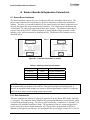
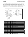
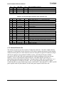
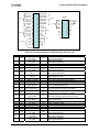
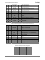
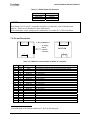
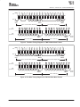
1
Imote2 Hardware Reference Manual Revision A, September 2007 PN: 7430-0409-01 © 2007 Crossbow Technology, Inc. All rights reserved. Information in this document is subject to change without notice. Crossbow, IRIS, MICA, TrueMesh and XMesh are trademarks of Crossbow Technology, Inc. Other product and trade names are trademarks or registered trademarks of their respective holders. Imote2 Hardware Reference Manual Table of Contents 1 Introduction.............................................................................................................................3 2 Imote2 Radio Processor Board (IPR2400) ...........................................................................4 2.1 Features.......................................................................................................................... 5 2.2 Mechanical Dimensions................................................................................................. 5 3 Processor..................................................................................................................................6 4 Radios and Antenna ...............................................................................................................7 5 4.1 Radio.............................................................................................................................. 7 4.2 Antenna.......................................................................................................................... 8 Power .......................................................................................................................................9 5.1 6 Sensor Boards & Expansion Connectors............................................................................11 6.1 7 8 Sensor Board Interfaces ............................................................................................... 11 ITS400 Basic Sensor Board..................................................................................................17 7.1 Sensor Suite ................................................................................................................. 17 7.2 Boost Switcher and Linear Regulator .......................................................................... 19 7.3 Communication and Addressing.................................................................................. 19 7.4 Pin-out Description ...................................................................................................... 20 7.5 Hardware Errata (Board Rev 2.0) ................................................................................ 21 IIB2400 Interface Board ......................................................................................................22 8.1 9 Power Supply Options ................................................................................................... 9 Connector Description ................................................................................................. 23 Appendix A. Warranty and Support Information ............................................................24 9.1 Customer Service......................................................................................................... 24 9.2 Contact Directory......................................................................................................... 24 9.3 Return Procedure ......................................................................................................... 24 9.4 Warranty ...................................................................................................................... 25 Doc. # 7430-0409-01 Rev. A Page 1 Imote2 Hardware Reference Manual About This Document The following annotations have been used to provide additional information. ; NOTE Note provides additional information about the topic. EXAMPLE Examples are given throughout the manual to help the reader understand the terminology. IMPORTANT This symbol defines items that have significant meaning to the user WARNING The user should pay particular attention to this symbol. It means there is a chance that physical harm could happen to either the person or the equipment. The following paragraph heading formatting is used in this manual: 1 Heading 1 1.1 Heading 2 1.1.1 Heading 3 This document also uses different body text fonts (listed in Table 0-1) to help you distinguish between names of files, commands to be typed, and output coming from the computer. Table 0-1. Font types used in this document. Font Type Usage Courier New Normal Sample code and screen output Courier New Bold Commands to be typed by the user Times New Roman Italic TinyOS files names, directory names Franklin Medium Condensed Page 2 Text labels in GUIs Doc. # 7430-0409-01 Rev. A Imote2 Hardware Reference Manual 1 Introduction This User’s Manual describes the hardware features of the Imote2 Processor Radio (IPR2400) board and basic sensor board (ITS400). Table 1-1 below lists the models covered in this Manual. Table 1-1. Imote2 Models covered in the Reference Manual Model Number IPR2400 ITS400 Description Imote2 processor radio board Imote2 basic sensor board This Manual is not a software guide to programming the Imote2, nor is it a guide to pre-built software packages that run on top of the Motes. The following resources are available regarding software: Imote2.Builder SDK Manual by Crossbow Technology, Inc. Imote2 Yahoo Users group at http://tech.groups.yahoo.com/group/intel-mote2-community/ Intel Imote2 resources page at http://www.intel.com/research/sensornets/ Doc. # 7430-0409-01 Rev. A Page 3 Imote2 Hardware Reference Manual 2 Imote2 Radio Processor Board (IPR2400) The Crossbow Imote2 is an advanced sensor network node platform designed for demanding wireless sensor network applications requiring high CPU/DSP and wireless link performance and reliability. The platform is built around Intel’s XScale® processor, PXA271. It integrates an 802.15.4 radio (TI CC2420) with an on-board antenna. It exposes a “basic sensor board” interface, consisting of two connectors on one side of the board, and an “advanced sensor board” interface, consisting of two high density connectors on the other side of the board. The Imote2 is a modular stackable platform and can be stacked with sensor boards to customize the system to a specific application, along with a “battery board” to supply power to the system. USB Connector Reset Button Figure 2-1. Photos of the Imote2 Board Antenna GPIOs 802.15.4 radio 2x SPI 32MB FLASH 3x UART SMA I2C SDIO XScale CPU core 32MB SDRAM I/O USB host USB client AC’97 256kB SRAM XScale DSP Camera I2S Power management Supply RTC Battery charger Figure 2-2. Imote2 Block diagram Page 4 Doc. # 7430-0409-01 Rev. A Imote2 Hardware Reference Manual 2.1 Features • • • • • • • • • PXA271 XScale® processor @ [13–416] MHz Wireless MMX coprocessor 256kB SRAM, 32MB FLASH, 32MB SDRAM Integrated 802.15.4 radio, support for external radios through SDIO and UART Integrated 2.4GHz antenna Multicolor status indicator LED Basic and advanced expansion connectors supporting : 3xUART, I2C, 2xSPI, SDIO, I2S, AC97, USB host, Camera I/F, GPIO Mini-USB port for direct PC connection Size: 48 mm x 36 mm. PCB Thickness 1.75 mm Table 2-1. Imote2 Operating Specifications 2.2 Parameter Operating Value Supply Voltage (Vbat) 5.5 V Charger Input Voltage (Vchg) 10 V Input Voltage (Vin) VCC io ± 0.3 V Storage Temperature -40 to +1250 C Operating Temperature 0 to +850 C Current in deep sleep mode 387 µA Current in active mode (13 MHz, radio off) 31 mA Current in active mode (13 MHz, radio Tx/Rx) 44 mA Current in active mode (104 MHz, radio Tx/Rx) 66 mA Mechanical Dimensions Figure 2-3. Mechanical Outline Drawing of OEM Edition Module Doc. # 7430-0409-01 Rev. A Page 5 Imote2 Hardware Reference Manual 3 Processor The Imote2 contains the PXA271 processor. This processor can operate in a low voltage (0.85V) and a low frequency (13 MHz) mode, hence enabling low power operation. The frequency can be scaled to 104 MHz at the lowest voltage level, and can be increased up to 416MHz with Dynamic Voltage Scaling. The processor has many low power modes, including sleep and deep sleep modes. It also integrates 256 KB of SRAM divided into 4 equal banks of 64 KB. The PXA271 is a multi-chip module that includes three chips in a single package, the processor, 32 MB SDRAM and 32 MB of flash. The processor integrates many I/O options making it extremely flexible in supporting different sensors, A/Ds, radio options, etc. These I/O options include I2C, 3 Synchronous Serial Ports one of which dedicated to the radio, 3 high speed UARTs, GPIOs, SDIO, USB client and host, AC97 and I2S audio codec interfaces, fast infrared port, PWM, Camera Interface and a high speed bus (Mobile Scaleable Link). The processor also adds many timers and a real time clock. The PXA271 also includes a wireless MMX coprocessor to accelerate multimedia operations. It adds 30 new media processor instructions, support for alignment and video operations and compatibility with Intel MMX and SSE integer instructions. Page 6 Doc. # 7430-0409-01 Rev. A Imote2 Hardware Reference Manual 4 Radios and Antenna 4.1 Radio The Imote2 integrates an 802.15.4 radio transceiver from ChipCon (CC2420). 802.15.4 is an IEEE standard describing the physical & MAC layers of a low power low range radio, aimed at control and monitoring applications. The CC2420 supports a 250 kb/s data rate with 16 channels in the 2.4 GHz band. Other external radio modules such as 802.11 and Bluetooth can be enabled through the supported interfaces (SDIO, UART, SPI, etc). 4.1.1 Radio RF Channel Selection The Imote2’s CC2420 radio can be tuned within the IEEE 802.15.4 channels that are numbered from 11 (2.405 GHz) to 26 (2.480 GHz) each separated by 5 MHz. 4.1.2 Radio Transmission Power RF transmission power is programmable from 0 dBm (1 mW) to –25dBm. Lower transmission power can be advantageous by reducing interference and dropping radio power consumption from 17.5 mA at full power to 8.5 mA at lowest power. Table 4-1. Chipcon® CC2420 Output Power Settings and Typical Current Consumption RF Power (dBm) Power Register (code) 0 -1 -3 -5 -7 -10 -15 -25 31 27 23 19 15 11 7 3 Current Consumption (mA) 17.4 16.5 15.2 13.9 12.5 11.2 9.9 8.5 The RF received signal strength indication (RSSI) is read directly from the CC2420 Radio and sent with every radio packet received. Typical RSSI values for a given RF input level are shown in Figure 4-1 below. Doc. # 7430-0409-01 Rev. A Page 7 Imote2 Hardware Reference Manual Figure 4-1. Typical RSSI value versus input RF level in dBm 4.2 Antenna The Imote2 platform integrates a 2.4 GHz surface mount antenna which provides a nominal range of about 30 meters. If a longer range is desired, an SMA connector can be soldered directly to the board to connect to an external antenna. There are literally hundreds of antenna options offered by different vendors and some references are provided below: • Linx Technologies: http://www.linxtechnologies.com/ • Nearson: http://www.nearson.com/ Page 8 Doc. # 7430-0409-01 Rev. A Imote2 Hardware Reference Manual 5 Power 5.1 Power Supply Options To supply the processor with all the required voltage domains, the Imote2 includes a Power Management IC. This PMIC supplies 9 voltage domains to the processor in addition to the Dynamic Voltage Scaling capability. It also includes a battery charging option and battery voltage monitoring. Two of the PMIC voltage regulators (1.8 V & 3.0 V) are used to supply the sensor boards with the desired regulated supplies at a maximum current of 200 mA. The processor communicates with the PMIC over a dedicated I2C bus (PWRI2C). The Imote2 platform was designed to support primary and rechargeable battery options as described below, in addition to being powered via USB. The following figure shows how the different battery boards and on board connectors can be used to power the mote. 5.1.1 Primary Battery The Imote2 platform can be powered using primary batteries with a voltage range of 3.2 - 4.5 V (e.g. 3 AAA alkaline batteries). A battery board with a basic or advanced set of connectors can be connected to the Vbat pins of the connector. As shown in the figure below, a diode and fuse should be connected between the battery and mote board to protect the battery and the PMIC. 5.1.2 Rechargeable Battery A rechargeable battery can be used to supply power to the Imote2 platform by connecting it directly to the Vbat pin on the connector. In this case, the PMIC battery charger can be used to recharge the batteries. The battery board should drive the nCHARGE_EN pin low to connect the USB input to the PMIC charger pin, hence allowing to recharge the battery using USB. The PMIC supports single cell Li-Ion at 4.1 and 4.2 V, in addition to a Li-Polymer pack. See the figure below for more details. 5.1.3 Mini-USB connector input The mote can be powered directly from USB, by routing the USB power to the Vbat input of the PMIC. This is the default state when either a battery is not connected, or when a battery board drives the nCHARGE_EN input high (as the case with all primary battery boards). If a battery board pulls nCHARGE_EN low, the USB input gets routed to the Vchg pin of the PMIC, which would be the case for rechargeable batteries as mentioned above. 5.1.4 On-board pads The On board pads can be used to connect a primary battery directly to the mote. A diode is included in this path to protect the primary battery. In addition, these pads can be used to connect any power source supplying a voltage range of 3.2 – 4.5V (after the diode drop). This connector is similar to the USB connector functionality, as it could be used to supply power to the mote or to recharge a battery based on the state of the nCHARGE_EN pin. The PMIC is also used to enable the alarm functionality that is exposed on the basic and advanced sensor connectors. When power is supplied to the mote, the PMIC will start, however it will not start the mote until the power button is pushed (similar to a cell phone usage model). Doc. # 7430-0409-01 Rev. A Page 9 Imote2 Hardware Reference Manual If it is desired to have a power board automatically turn on the mote, the power board can short the alarm pin on the connector to the VRTC pin. This will cause the mote to start automatically every time power is applied to the mote. However, if a more intelligent sensor board is desired to start the mote in response to a specific sensor event, the alarm pin can be controlled by the sensor board to start/wakeup the mote selectively. Diode forward voltage drop 0.5V -> 1.1V Ihold = 0.5 A Itrip = 1A Vchg = 4.6V – 10V Vbat = 3.2V – 4.5V Figure 5-1. Power supply options for Imote2 Page 10 Doc. # 7430-0409-01 Rev. A Imote2 Hardware Reference Manual 6 Sensor Boards & Expansion Connectors 6.1 Sensor Board Interfaces The Imote2 platform exposes two sets of connectors, the basic set and the advanced set. The pins on each connector set are split into two physical connectors to enhance the mechanical stability. The basic set is meant to enable low cost sensor boards (low density connectors were chosen) and support the most common sensor interfaces. This connector set is defined as the “architectural” set, and can be supported in future mote designs. The advanced connector set exposes some of the PXA271 advanced features (Camera Interface, High speed bus, Audio interfaces, etc), and is assumed to be platform specific. The details of the connector sets are described below. Top J7 16 1 31 17 Hirose DF9-31P-1V Bottom J4 20 1 40 21 Hirose DF15B-40DS-0.65V Hirose DF15-20DS-0.65V 10 1 20 11 J3 Hirose DF9-21P-1V 11 1 21 12 J5 Figure 6-1. Connector information for Imote2 Table 6-1. Matching connector information Description Manufacturer Part# 40 pin (J4) Hirose DF15B(3.2)-40DP-0.65V 20 pin (J3) Hirose DF15B(3.2)-20DP-0.65V 31 pin (J1) Hirose DF9-31S-1V 21 pin (J5) Hirose DF9-21S-1V ; NOTE: The Hirose DF15 connector type comes in wide variety of stacking heights. Using the recommended part numbers will result in a 5mm stacking height on the bottom side. If desired, an expansion board designer can choose a different part number of the DF15 connector used in order to meet custom stacking height requirements. 6.1.1 Basic Connector Set The basic connector set consists of 2 physical connectors from the Hirose DF9 family which has a 1 mm pitch. The connector choice simplifies the routing and soldering of sensor boards, which is useful in the prototyping stage. The pins are split between the 2 connectors (31 pin and 21 pin connectors) for mechanical stability reasons. The asymmetry of the two connectors provides a useful visual clue of sensor board orientation. All I/O pins can be programmed as GPIOs in addition to their special port function. As mentioned in the power supply section, the 1.8 and 3.0 Doc. # 7430-0409-01 Rev. A Page 11 Imote2 Hardware Reference Manual V pins are supplied by the PMIC and can be used to power the sensor boards. The alarm pin is an input pin and can be used by the sensor boards to wake up the processor out of deep sleep mode if needed. The reset pin is an input pin to force a hardware reset of the processor. The standard UART will be used as the debug console and is exposed on the 21 pin connector. The 31 pin connector exposes 2 high speed UART ports, 2 SSP ports, an SDIO port, an I2C port and multiple GPIOs. There are 11 reserved pins to allow for future expansion and inter-board communication. 31 pin UART 2 FFRxD 1 FFTxD 2 FFCTS UART 1 FFRTS 4 BTRxD 5 BTTxD 6 7 8 BTCTS BTRTS GND SSPCLK2 SPI 2 3 SSPFRM2 SSPTxD2 SSPRxD2 GPIO 9 10 11 12 13 14 Reserved Reserved 15 21 pin 17 SCL 18 SDA 19 SSPCLK 20 SSPFRM 21 SSPTxD 22 SSPRxD GPIO 23 24 25 GND 26 MMCMD 27 28 29 I2C SPI 1 Future expansion MMCLK MMD0 MMD1 B2B comm MMD3 31 GPIO 1 VBAT 12 2 GND Reserved PMIC_TBAT 13 3 14 USB5V H_5V 5 Reserved 6 7 8 Reserved Reserved Reserved Reserved Reserved 4 9 10 11 15 16 1.8 V 3.0 V Reserved Alarm Reset 17 GND 18 VRTC nCHARGE_EN 19 20 21 STD_RxD STD_TxD STDUart SDIO Hirose DF9 MMD2 30 VBAT 16 Hirose DF9 Table 6-2. Pin-out description for basic large connector (J7) Pin# Type Name GPIO# 1 2 3 4 5 6 7 8 9 10 11 12 13 14 15 16 17 18 19 20 21 22 23 24 25 I/O I/O I/O I/O I/O I/O I/O I/O FF_RXD FF_TXD FF_CTS FF_RTS BT_RXD BT_TXD BT_CTS BT_RTS GND SSP2_SCLK SSP2_SFRM SSP2_TXD SSP2_RXD GPIO94 Reserved Reserved I2C_SCL I2C_SDA SSP1_SCLK SSP1_SFRM SSP1_TXD SSP1_RXD GPIO10 GND MM_CLK 96 99 100 98 42 43 44 45 Page 12 I/O I/O I/O I/O I/O R R I/O I/O I/O I/O I/O I/O I/O I/O 36 37 38 11 94 117 118 23 24 25 26 10 32 Description UART 1 receive data UART 1 send data UART 1 clear to send UART 1 request to send UART 2 receive data UART 2 send data UART 2 clear to send UART 2 request to send Ground Synchronous Serial Port 2 clock Synchronous Serial Port 2 frame Synchronous Serial Port 2 transmit data Synchronous Serial Port 2 receive data General purpose I/O Do not connect Do not connect I2C serial clock I2C serial data/address bus Synchronous Serial Port 1 clock Synchronous Serial Port 1 frame Synchronous Serial Port 1 transmit data Synchronous Serial Port 1 receive data General purpose I/O Ground MMC and SD/SDIO bus clock Doc. # 7430-0409-01 Rev. A Imote2 Hardware Reference Manual 26 27 28 29 30 31 I/O I/O I/O I/O I/O I/O MM_CMD MM_DAT0 MM_DAT1 MM_DAT2 MM_DAT3 GPIO93 112 92 109 110 111 93 MMC and SD/SDIO command MMC and SD/SDIO read / write data 0 MMC and SD/SDIO read / write data 1 MMC chip select 0 or SD/SDIO read / write data 2 MMC chip select 1 or SD/SDIO read / write data 3 General purpose I/O Table 6-3. Pin-out description for basic small connector (J5) Pin# 1 2 3 4 5 6 7 8 9 10 11 12 13 14 15 16 17 18 19 20 21 Type I R R R R R R R I O I I/O I/O Name VBAT VBAT GND PMIC_TBAT USBH_5V Reserved Reserved Reserved N/C N/C N/C VCC_1P8 VCC_3V Reserved ALARM NRESET GND VCC_RTC nCHARGE_EN STD_RXD STD_TXD GPIO# 46 47 Description Power Supply Rail (3.2 – 4.7 V minus Diode Drop) Power Supply Rail (3.2 – 4.7 V minus Diode Drop) Ground Battery temperature input 5.0 V supply rail to power sensor board (USBH) Do not connect Do not connect Do not connect Available for communication between expansion boards Available for communication between expansion boards Available for communication between expansion boards 1.8 V supply rail to power sensor boards 3.0 V supply rail to power sensor boards Do not connect Alarm input to PMIC (see power subsystem) Processor reset Ground Power supply for the RTC voltage domain of the PXA Battery select, 0 : rechargeable battery, 1 : primary battery UART 3 receive data UART 3 send data 6.1.2 Advanced Connector Set The advanced connector set also consists of 2 physical connectors. We chose a higher density connector (0.65mm pitch) for the advanced set to be able to support the large pin count required without increasing the size of the connector too much. The pins are split on 2 connectors (40 pin and 20 pin connectors) for mechanical stability reasons. Note that all I/O pins (with the exception of JTAG and USB) can be programmed as GPIOs in addition to their special port function. JTAG is exposed on the 20 pin connector. The MSL interface provides two independent high speed unidirectional links. The data-channel width can be scaled from 1 to 4 bits, providing up to 192 Mbps at 48 MHz. The CIF port supports the Intel Quick Capture Camera Interface, to easily attach image sensors to the Imote2. Note that the I2C, UART and SPI ports exposed on the 40 pin connector, are the same ports exposed on the basic side. Doc. # 7430-0409-01 Rev. A Page 13 Imote2 Hardware Reference Manual 40 pin MSL & CF BB_IB_DATA0 BB_IB_DATA1 1 21 2 22 BB_OB_DATA1 BB_IB_DATA2 3 23 BB_OB_DATA2 BB_IB_DATA3 BB_IB_CLK BB_IB_STB 4 24 25 BB_OB_DATA3 6 7 8 26 BB_OB_STB 27 9 29 30 BB_OB_WAIT GND CIF_DD9 BB_IB_WAIT USB Host I2S or AC97 FF UART GND USBH_N 5 USBH_P 10 28 BB_OB_DATA0 20 pin MSL & CF BB_OB_CLK JTAG nTRST TCK 1 11 2 12 TMS 3 13 TDO 4 14 TDI 5 15 GND 6 7 8 16 17 Reset Alarm 18 5V 9 19 3.0V 10 20 1.8V PMIC_TBAT Reserved CIF_DD8 GND I2S_BITCLK 11 12 31 32 CIF_DD7 I2S_DATAIN I2S_DATAOUT I2S_SYNC I2S_SYSCLK 13 33 GND VBAT VBAT 14 34 GPIO VBAT 15 35 SSPRxD GND 16 36 FFRTS FFCTS 17 37 SSPTxD SSPFRM CF CIF_DD6 SPI 1 STD_TxD STD_RxD STD Uart nCHARGE_EN VCC_RTC Hirose DF15 SSPCLK 18 38 FFTXD 19 39 SDA FFRXD 20 40 SCL I2C Hirose DF15 Table 6-4. Pin-out description for advanced large connector (J4) Pin# Type 1 I/O 2 I/O 3 4 I/O I/O 5 I/O 6 I/O 7 I/O 8 9 10 I/O I/O 11 I/O 12 I/O 13 I/O 14 I/O 15 I/O 16 17 18 19 20 I/O I/O I/O I/O 21 I/O 22 I/O 23 I/O Page 14 Name BB_IB_DATA0 CIF_DD5 BB_IB_DATA1 CIF_DD1 BB_IB_DATA2 BB_IB_DATA3 BB_IB_CLK CIF_DD4 BB_IB_STB CIF_FV BB_IB_WAIT CIF_LV GND USBH_N_CONN USBH_P_CONN I2S_BITCLK AC97_BITCLK I2S_DATA_IN AC97_SDATA_IN_0 I2S_DATA_OUT AC97_SDATA_OUT I2S_SYNC AC97_SYNC I2S_SYSCLK AC97_RESET_n GND FF_RTS FF_CTS FF_TXD FF_RXD BB_OB_DATA0 CIF_DD0 BB_OB_DATA1 CIF_DD5 BB_OB_DATA2 CIF_DD3 GPIO# 82 55 56 57 83 84 85 28 29 30 31 113 98 100 99 96 81 48 50 Description MSL inbound data bit 0 Quick capture data line 5 MSL inbound data bit 1 Quick capture data line 1 MSL inbound data bit 2 MSL inbound data bit 3 MSL inbound clock strobe Quick capture data line 4 MSL inbound signal qualifier Quick capture frame start MSL wait indicator for inbound link Quick capture line start Ground Data negative differential signal (USB D-) Data positive differential signal (USB D+) I2S bit clock, supplies the serial audio bit rate AC97 12.288-MHz bit-rate clock I2S Serial audio input data from CODEC AC97 Serial audio input data from CODEC I2S Serial audio output data to CODEC AC97 Serial audio output data to CODEC I2S SYNC, BITCLCK divided by 64 AC97 48-KHz frame indicator and synchronizer I2S system clock = BITCLK x 4 AC97 CODEC reset Ground UART 1 request to send UART 1 clear to send UART 1 send data UART 1 receive data MSL outbound data bit 0 Quick capture data line 0 MSL outbound data bit 1 Quick capture data line 5 MSL outbound data bit 2 Quick capture data line 3 Doc. # 7430-0409-01 Rev. A Imote2 Hardware Reference Manual 24 I/O 25 I/O 26 I/O 27 I/O 28 29 30 31 32 33 34 35 36 37 38 39 40 I/O I/O I/O I/O I/O I/O I/O I/O I/O I/O I/O BB_OB_DATA3 CIF_DD2 BB_OB_CLK CIF_DD4 BB_OB_STB CIF_MCLK BB_OB_WAIT CIF_PCLK GND CIF_DD9 CIF_DD8 CIF_DD7 CIF_DD6 GND GPIO10 SSP1_RXD SSP1_TXD SSP1_SFRM SSP1_SCLK I2C_SDA I2C_SCL 51 52 53 54 106 107 12 17 10 26 25 24 23 118 117 MSL outbound data bit 3 Quick capture data line 2 MSL outbound clock strobe Quick capture data line 4 MSL outbound signal qualifier Quick capture programmable output clock MSL wait indicator for outbound link Quick capture pixel clock Ground Quick capture data line 9 Quick capture data line 8 Quick capture data line 7 Quick capture data line 6 Ground General purpose I/O Synchronous Serial Port 1 receive data Synchronous Serial Port 1 transmit data Synchronous Serial Port 1 frame Synchronous Serial Port 1 clock I2C serial data I2C serial clock Table 6-5. Pin-out description for advanced small connector (J3) Pin# Type Name 1 2 3 4 5 6 7 8 9 10 11 12 I I I O I I I O JTAG_NTRST JTAG_TCK JTAG_TMS JTAG_TDO JTAG_TDI PMIC_TBAT GND VBAT VBAT VBAT STD_RXD STD_TXD 13 I nCHARGE_EN 14 15 16 17 18 19 20 O I GPIO# VCC_BAT_RTC GND NRESET ALARM VCC_5V VCC_3V VCC_1P8 Description JTAG port : Test Reset JTAG port : Test clock JTAG port : Test mode select JTAG port : Test data out JTAG port : Test data in Battery temperature input Ground Power Supply Rail (3.2 – 4.7 V minus Diode Drop) Power Supply Rail (3.2 – 4.7 V minus Diode Drop) Power Supply Rail (3.2 – 4.7 V minus Diode Drop) UART 3 receive data UART 3 send data Battery select, 0 : rechargeable battery, 1 : primary battery Power supply for the RTC voltage domain of the CPU Ground Processor reset Alarm input to PMIC (see power subsystem) 5.0 V supply rail to power sensor board (USBH) 3.0 V supply rail to power sensor boards 1.8 V supply rail to power sensor boards Table 6-6. Imote2 Internal I/O configuration Doc. # 7430-0409-01 Rev. A Component Pin name GPIO# LED Red 103 LED Green 104 LED Blue 105 CC2420 FIFO 114 CC2420 VREG_EN 115 CC2420 CCA 116 Page 15 Imote2 Hardware Reference Manual CC2420 FIFOP 0 CC2420 RESETN 22 CC2420 SFD 16 Table 6-7. Imote2 Test Points Test Point Name Page 16 Signal TP3 PWR pad for direct battery connection TP4 GND pad for direct battery connection TP5 STD_TXD TP6 STD_RXD TP7 PWR_SCL TP8 PWR_SDA TP9 13 MHz to PMIC TP14 PWR_EN TP15 SYS_EN TP16 NVDD_FAULT TP17 NBATT_FAULT Doc. # 7430-0409-01 Rev. A Imote2 Hardware Reference Manual 7 ITS400 Basic Sensor Board The basic sensor board is designed to connect to the basic connectors on the Imote2. It contains a 3d Accelerometer, advanced temp/humidity sensor, light sensor and 4 channel A/D. It is a pass through board to allow stacking with another sensor/communication board. Figure 7-1. Photo of the ITS400 Sensor Board SPI GPIO External connector 4 Humidity Temperature 3D Acceleration Power regulator 0-3V ADC Temperature Light I2C Figure 7-2. ITS400 Block diagram Table 7-1. ITS400 Operating Specifications Parameter Operating temperature range Storage temperature range Humidity (non condensing) Operating Value 0 to +70 ºC -40 to +150 ºC 80 % 7.1 Sensor Suite The ITS400 sensor board is multi-sensor board that combines a popular set of sensors for wireless sensor network applications, including: Doc. # 7430-0409-01 Rev. A Page 17 Imote2 Hardware Reference Manual • • • • • ST Micro LIS3L02DQ 3d 12 bit ±2g accelerometer High Accuracy, ±0.3°C Sensirion SHT15 temperature/humidity sensor TAOS TSL2651Light Sensor Maxim MAX1363 4 Channel General Purpose A/D for quick prototyping TI Tmp175 Digital Temperature Sensor with two-wire interface 7.1.1 3D Accelerometer This board includes an ST Micro LIS3L02DQ 3d accelerometer. This sensor has a range of +/2g with 12 bit resolution. It offers two possible interfaces, SPI or I2C, either of which is selectable using 0-ohm resistors including on the board. To communicate with the sensor using the I2C interface, populate R17 and remove R21. To communicate with the sensor using SPI, populate R21 and remove R17. By default, the sensor is connected to SSP1 on the Intel Mote 2. In the event that another stacked board conflicts with the basic sensor board use of SSP1, the sensor may be disconnected from the port by removing R23, R24, R25 and R26, and connected to SSP2 instead by populating R29, R30, R31, R32 with zero ohm resistors. The sensor’s data ready (RDY_INT) interrupt is connected to GPIO96 through an OR gate as shown in the schematic below. If another board conflicts with the use of GPIO 96, the BT_RXD pin can be used instead by loading R34. For more info on this sensor, the datasheet can be found at http://www.stmicro.fr/stonline/products/literature/ds/10175.pdf. 7.1.2 Temperature and Humidity Sensor The boards include a Sensirion SHT15 sensor which can be used for applications requiring high accuracy temp reading (+/- 0.3 degC) and humidity. This sensor interfaces to the Intel Mote 2 through two GPIO pins. The data pin of the SHT11 is connected to GPIO 100, whereas the clock pin is connected to GPIO 98. Another set of connections is available by loading R36 and R37 if no conflict exists with another stacked board. For more information on the SHT11 sensor, please reference its datasheet located at: http://www.sensirion.com/images/getFile?id=25 Page 18 Doc. # 7430-0409-01 Rev. A Imote2 Hardware Reference Manual 7.1.3 Light Sensor The board includes a TAOS TSL2651 light sensor. This sensor interfaces to the Intel Mote 2 through the I2C bus. The interrupt pin (LIGHT_INT) is connected to GPIO99 through a NAND gate as shown in the schematic above. If another board conflicts with the use of GPIO 99, the BT_TXD pin can be used instead by loading R35. The address select line is driven by R4 and R6 and is set to 1 by default (R4 in, R6 out). To set it to 0, populate R6 and remove R4. To float it, remove both R4 and R6. Refer to data sheet for address mapping. The data sheet can be found at http://www.taosinc.com/product_detail.asp?cateid=4&proid=60 7.1.4 General purpose A/D The board includes a Maxim MAX1363, 4 channel, 12 bit resolution general purpose ADC for quick prototyping. Each channel supports 0-3 V input signals. The ADC interfaces to the Intel Mote 2 through the I2C bus. The analog pins are brought out to a Molex PN-39357-0003 connector (J5) and the pin assignment is shown below. Pin A0 which controls the I2C address of the ADC is driven to 0 by default (R7 out, R9 in). If the I2C address needs to be changed, A0 can be driven to 1 (as specified in the data sheet) by removing R9 and populating R7. The interrupt line (ANALOG_INT) is connected to GPIO99 through a NAND gate as shown in schematic above. If another board conflicts with the use of GPIO 99, the BT_TXD pin can be used instead by loading R35. The datasheet can be found at http://pdfserv.maximic.com/en/ds/MAX1363-MAX1364.pdf. 7.1.5 Digital Temperature Sensor with two wire interface The board includes a TI TMP175, a digital temperature sensor with a two wire output serial interface. The device is capable of a ± 1.5°C accurate over the range of -25°C to +85°C. The sensor allows up to 27 I2C devices on the bus. TMP175 address can be configured via resistors R13,R14,R15,R16,R27,R28. See schematic and TMP175 datasheet for more details. The interrupt line(TEMP_ALERT) is connected to GPIO96(FF_TXD) as shown in the schematic above. The datasheet for the device can be found at http://focus.ti.com/lit/ds/symlink/tmp175.pdf 7.2 Boost Switcher and Linear Regulator The board includes a switching voltage regulator (U11-LTC3426), followed by linear regulator (U12-LTC1962). The input to the boost regulator is provided from the battery. In order to provide a cleaner power supply the output of the switcher is regulated further with a linear regulator. Regulated voltage output is provided externally through the connector J5 pin 5. It could be used for prototyping purposes in the case where a user of the board requires a voltage that is higher than anything provided by the board. All boards are shipped with the switcher/regulator disabled. See schematic and datasheet details on how to enable the switcher and set the voltages on both the switcher and the regulator. 7.3 Communication and Addressing The Light Sensor (U2), Simple Temp Sensor (U7) and general purpose A/D (U1) can only be accessed via the I2C bus. Resistor settings control device addressing. Doc. # 7430-0409-01 Rev. A Page 19 Imote2 Hardware Reference Manual Table 7-2. ITS400 Default I2C addresses Sensor Address TS2561(U2) TMP175(U7) MAX1363(U1) 1001001 1001010 0110100 ; NOTE: Temp Sensor (U6) is not I2C compatible and utilizes a proprietary serial communication protocol. Please see its datasheet for more information. 3D Accelerometer can be configured to communicate over either I2C or SPI serial buses. 7.4 Pin-out Description 16……………….1 31………...…17 J4 1……………….16 17………...…31 « “B” Connectors » J5 Analog Sensor Interface Connector J2 BOTTOM J1 J3 11….….1 21….12 1….….11 12….21 Table 7-3. ITS400 Pin-out description for Small “A” connector 1 Pin # Type Name A11 A21 A3 A41 A5 A6 A7 A8 A9 A10 A11 A121 A131 A141 A151 A161 A17 A181 A191 A201 A211 PWR PWR VBAT VBAT GND PMIC_TBAT Reserved Reserved Reserved Reserved Reserved Reserved Reserved 1.8V 3.0V Reserved Alarm Reset GND VRTC nCHARGE_EN STD_RXD STD_TXD PWR R R R R R R R PWR PWR R Description Not used by the sensor board, serves as input to the switcher Not used by the sensor board, serves as input to the switcher Ground Not used by the sensor board Do not connect Do not connect Do not connect Do not connect Do not connect Do not connect Do not connect Not used by the sensor board Sensor Board Power Supply Do not connect Not used by the sensor board Not used by the sensor board Ground Not used by the sensor board Not used by the sensor board Not used by the sensor board Not used by the sensor board Passed through to the bottom connectors J3 & J4 on the same pins. Page 20 Doc. # 7430-0409-01 Rev. A Imote2 Hardware Reference Manual Table 7-4. ITS400 Pin-out description Large “B” connector Pin # Type Name B1 O FF_RXD B2 O FF_TXD B3 B4 B51 B61 B71 B81 B9 B101 B111 B121 B131 B141 B15 B16 B171 B181 B191 B201 B211 I/O I R R I I/O I/O I I FF_CTS FF_RTS BT_RXD BT_TXD BT_CTS BT_RTS GND SSP2_SCLK SSP2_SFRM SSP2_TXD SSP2_RXD GPIO_94 RFU8 RFU9 I2C_SCL/SCL_SPC I2C_SDA/SDL_SDI_SDO SSP1_SCLK/SCL_SPC SSP1_SFRM/SPI_CS SSP1_TXD/SDA_SDI_SDO B221 O SSP1_RXD/SDO 1 Description Logical OR of RDY_INT and TEMP_ALERT(Note1.1) Logical NAND of LIGHT_INT and ANALOG_INT(Note1.2) Serial Data for SHT15 Serial Clock for SHT15 An alternative connection to B1 An alternative connection to B2 An alternative connection to B3 An alternative connection to B4 Ground An alternative connection to B19 An alternative connection to B20 An alternative connection to B21 An alternative connection to B22 Not used by the sensor board Do not connect Do not connect I2C Clock/SPI Serial Port Clock I2C Data/SPI Serial Data Input SPI serial clock SPI chip select SPI serial data input for accelerometer SPI serial data output for accelerometer B23 GPIO10 B24 B251 GND MM_CLK Not used by the sensor board B261 MM_CMD Not used by the sensor board B271 MM_DATA0 Not used by the sensor board B281 MM_DATA1 Not used by the sensor board B291 MM_DATA2 Not used by the sensor board 1 B30 MM_DATA3 Not used by the sensor board B31 GPIO_93 Not used by the sensor board Not used by the sensor board Ground Table 7-5. ITS400 Pin-out description J5-Analog Sensor Interface Connector Pin # Type Name Description 1 Analog Input AIN0 Input to an ADC 2 Analog Input AIN1 Input to an ADC 3 Analog Input AIN2 Input to an ADC 4 Analog Input AIN3 Input to an ADC 5 PWR 3V 6 7 8 GND I/O I/O GND I2C SDA I2C SCL Switcher/Regulator output supplied from the Sensor Board Ground I2C Data I2C Clock 7.5 Hardware Errata (Board Rev 2.0) U7(TMP175) TEMP_ALERT signal requires a 10Kohm pull up to 3V. It’s missing in the current revision. U2(TSL2561) LIGHT_INT signal requires a 10Kohm pull up to 3V. It’s missing in the current revision. Doc. # 7430-0409-01 Rev. A Page 21 Imote2 Hardware Reference Manual 8 IIB2400 Interface Board The IIB2400 interface board is used for code loading and debugging through JTAG. It connects to the Imote2 through the advanced connectors, and is a pass through board to enable debugging with other power/battery boards attached to the Imote2. Figure 8-1. Photo of the IIB2400 Interface Board Config Switch1 Config Switch2 Program Switch JTAG Interface Dual Port FTDI Chip Switching Fabric Xilinx XC2C64 CPLD SPI I2C FFUART STUART Imote2 Advanced Connector Figure 8-2. ITS400 Block diagram It contains a dual port FTDI chip, mapping the USB input to 2 serial ports. The first serial port connects to the STDUART on the Imote2 platform and is meant to be used for the console. The second serial port can be configured to connect to FFUART regular, FFUART crossover, I2C or Page 22 Doc. # 7430-0409-01 Rev. A Imote2 Hardware Reference Manual SSP1 ports. This mapping is controlled by the SW5 switch on the board and is labeled accordingly. The power supply can be controlled by the SW6 switch to select on of the following options: • Option 1 : USB power drives VBAT to power the mote (marked as “PWR”) • Option 2 : VBAT is not driven (marked as “No PWR”) The debug board is designed to work with both the Intel JTAG dongle and the Macgraigor Raven dongle. It provides the ability to program the mote as well as the on-board CPLD through JTAG. The desired JTAG chain is selected via the SW3 switch. 8.1 Connector Description J3 J4 1...............20 21..............40 20...............1 40..............21 1.......10 11.....20 10.......1 20.....11 J1 J2 TOP Bottom Table 8-1. Connector information Description Manufacturer Part # 40 pin Advanced (J3) Hirose DF15B(1.8)-40DP-0.65V(50) 20 pin Advanced (J1) Hirose DF15B(1.8)-20DP-0.65V(50) 40 pin Advanced (J4) Hirose DF15B(1.8)-40DS-0.65V(50) 20 pin Advanced (J2) Hirose DF15B(1.8)-20DS-0.65V(50) Doc. # 7430-0409-01 Rev. A Page 23 Imote2 Hardware Reference Manual 9 Appendix A. Warranty and Support Information 9.1 Customer Service As a Crossbow Technology customer you have access to product support services, which include: • Single-point return service • Web-based support service • Same day troubleshooting assistance • Worldwide Crossbow representation • Onsite and factory training available • Preventative maintenance and repair programs • Installation assistance available 9.2 Contact Directory United States: Phone: 1-408-965-3300 (8 AM to 5 PM PST) Fax: 1-408-324-4840 (24 hours) Email: [email protected] Non-U.S.: refer to website www.xbow.com 9.3 Return Procedure 9.3.1 Authorization Before returning any equipment, please contact Crossbow to obtain a Returned Material Authorization number (RMA). Be ready to provide the following information when requesting a RMA: • Name • Address • Telephone, Fax, Email • Equipment Model Number • Equipment Serial Number • Installation Date • Failure Date • Fault Description Page 24 Doc. # 7430-0409-01 Rev. A Imote2 Hardware Reference Manual 9.3.2 Identification and Protection If the equipment is to be shipped to Crossbow for service or repair, please attach a tag TO THE EQUIPMENT, as well as the shipping container(s), identifying the owner. Also indicate the service or repair required, the problems encountered and other information considered valuable to the service facility such as the list of information provided to request the RMA number. Place the equipment in the original shipping container(s), making sure there is adequate packing around all sides of the equipment. If the original shipping containers were discarded, use heavy boxes with adequate padding and protection. 9.3.3 Sealing the Container Seal the shipping container(s) with heavy tape or metal bands strong enough to handle the weight of the equipment and the container. 9.3.4 Marking Please write the words, “FRAGILE, DELICATE INSTRUMENT” in several places on the outside of the shipping container(s). In all correspondence, please refer to the equipment by the model number, the serial number, and the RMA number. 9.3.5 Return Shipping Address Use the following address for all returned products: Crossbow Technology, Inc. 4145 N. First Street San Jose, CA 95134 Attn: RMA Number (XXXXXX) 9.4 Warranty The Crossbow product warranty is one year from date of shipment. Doc. # 7430-0409-01 Rev. A Page 25 Crossbow Technology, Inc. 4145 N. First Street San Jose, CA 95134 Phone: 408.965.3300 Fax: 408.324.4840 Email: [email protected] TMP175 TMP75 SBOS288J − JANUARY 2004 − REVISED DECEMBER 2007 Digital Temperature Sensor with Two-Wire Interface FEATURES D 27 ADDRESSES (TMP175) 8 ADDRESSES (TMP75) DIGITAL OUTPUT: Two-Wire Serial Interface RESOLUTION: 9- to 12-Bits, User-Selectable D D D ACCURACY: D ±1.5°C (max) from −25°C to +85°C ±2.0°C (max) from −40°C to +125°C LOW QUIESCENT CURRENT: 50µA, 0.1µA Standby WIDE SUPPLY RANGE: 2.7V to 5.5V D D SMALL SO-8 AND MSOP-8 PACKAGES APPLICATIONS D POWER-SUPPLY TEMPERATURE D MONITORING COMPUTER PERIPHERAL THERMAL PROTECTION NOTEBOOK COMPUTERS CELL PHONES BATTERY MANAGEMENT OFFICE MACHINES THERMOSTAT CONTROLS DESCRIPTION The TMP175 and TMP75 are two-wire, serial output temperature sensors available in SO-8 and MSOP-8 packages. Requiring no external components, the TMP175 and TMP75 are capable of reading temperatures with a resolution of 0.0625°C. The TMP175 and TMP75 feature a Two-Wire interface that is SMBus-compatible, with the TMP175 allowing up to 27 devices on one bus and the TMP75 allowing up to eight devices on one bus. The TMP175 and TMP75 both feature an SMBus Alert function. The TMP175 and TMP75 are ideal for extended temperature measurement in a variety of communication, computer, consumer, environmental, industrial, and instrumentation applications. The TMP175 and TMP75 are specified for operation over a temperature range of −40°C to +125°C. Temperature D D D D D D ENVIRONMENTAL MONITORING AND HVAC D ELECTROMECHANICAL DEVICE SDA SCL ALERT 1 Diode Temp. Sensor 2 3 4 8 7 ∆Σ A/D Converter TEMPERATURE GND Control Logic OSC V+ A0 Serial Interface 6 Config. and Temp. Register 5 A1 A2 TMP175, TMP75 Please be aware that an important notice concerning availability, standard warranty, and use in critical applications of Texas Instruments semiconductor products and disclaimers thereto appears at the end of this data sheet. All trademarks are the property of their respective owners. Copyright 2004−2007, Texas Instruments Incorporated ! ! www.ti.com "#$% "$% www.ti.com SBOS288J − JANUARY 2004 − REVISED DECEMBER 2007 This integrated circuit can be damaged by ESD. Texas Instruments recommends that all integrated circuits be handled with appropriate precautions. Failure to observe proper handling and installation procedures can cause damage. ABSOLUTE MAXIMUM RATINGS(1) Power Supply, V+ . . . . . . . . . . . . . . . . . . . . . . . . . . . . . . . . . . . . 7.0V Input Voltage(2) . . . . . . . . . . . . . . . . . . . . . . . . . . . . . . −0.5V to 7.0V Input Current . . . . . . . . . . . . . . . . . . . . . . . . . . . . . . . . . . . . . . . 10mA Operating Temperature Range . . . . . . . . . . . . . . . −55°C to +127°C Storage Temperature Range . . . . . . . . . . . . . . . . . −60°C to +130°C Junction Temperature (TJ max) . . . . . . . . . . . . . . . . . . . . . . +150°C ESD Rating: Human Body Model (HBM) . . . . . . . . . . . . . . . . . . . . . . . 4000V Charged Device Model (CDM) . . . . . . . . . . . . . . . . . . . . 1000V Machine Model (MM) . . . . . . . . . . . . . . . . . . . . . . . . . . . . . . 300V (1) Stresses above these ratings may cause permanent damage. Exposure to absolute maximum conditions for extended periods may degrade device reliability. These are stress ratings only, and functional operation of the device at these or any other conditions beyond those specified is not supported. (2) Input voltage rating applies to all TMP175 and TMP75 input ESD damage can range from subtle performance degradation to complete device failure. Precision integrated circuits may be more susceptible to damage because very small parametric changes could cause the device not to meet its published specifications. voltages. ORDERING INFORMATION(1) PRODUCT PACKAGE-LEAD PACKAGE DESIGNATOR PACKAGE MARKING TMP175 SO-8 D TMP175 TMP175 MSOP-8 DGK DABQ TMP75 TMP75 SO-8 D TMP75 MSOP-8 DGK T127 (1) For the most current package and ordering information, see the Package Option Addendum at the end of this document, or see the TI website at www.ti.com. PIN ASSIGNMENTS Top View TMP175 ALERT 3 GND 4 SO−8 7 6 5 A0 A1 A2 SDA 1 SCL 2 ALERT 3 GND 4 8 7 6 5 MSOP−8 V+ A0 A1 A2 SDA 1 SCL 2 ALERT 3 GND 4 TMP75 8 V+ SDA 1 7 A0 SCL 2 6 A1 ALERT 3 5 A2 GND 4 SO−8 NOTE: Pin 1 is determined by orienting the package marking as indicated in the diagram. 2 T127 2 V+ TMP75 SCL 8 DABQ 1 TMP175 SDA TMP75 TMP175 MSOP−8 8 V+ 7 A0 6 A1 5 A2 "#$% "$% www.ti.com SBOS288J − JANUARY 2004 − REVISED DECEMBER 2007 ELECTRICAL CHARACTERISTICS At TA = −40°C to +125°C, and V+ = 2.7V to 5.5V, unless otherwise noted. TMP175 PARAMETER CONDITION MIN TYP TMP75 MAX MIN +125 −40 TYP MAX UNITS TEMPERATURE INPUT +125 °C −25°C to +85°C ±0.5 ±1.5 ±0.5 ±2.0 °C −40°C to +125°C ±1.0 ±2.0 ±1.0 ±3.0 °C 0.2 ±0.5 0.2 ±0.5 °C/V Range −40 Accuracy (Temperature Error) vs Supply Resolution(1) Selectable +0.0625 +0.0625 °C 3 3 pF DIGITAL INPUT/OUTPUT Input Capacitance Input Logic Levels: VIH VIL 0.7(V+) 6.0 0.7(V+) 6.0 −0.5 0.3(V+) −0.5 0.3(V+) V 1 µA 0V ≤ VIN ≤ 6V Leakage Input Current, IIN Input Voltage Hysteresis 1 SCL and SDA Pins 500 500 V mV Output Logic Levels: VOL SDA VOL ALERT IOL = 3mA IOL = 4mA Resolution Conversion Time 0 0.15 0.4 0 0.15 0.4 V 0 0.15 0.4 0 0.15 0.4 V Selectable 9 to 12 9-Bit 27.5 37.5 27.5 37.5 ms 10-Bit 55 75 55 75 ms 11-Bit 110 150 110 150 ms 12-Bit 220 300 220 300 ms 54 74 25 54 74 ms 5.5 2.7 Timeout Time 25 9 to 12 Bits POWER SUPPLY Operating Range Quiescent Current Shutdown Current 2.7 IQ Serial Bus Inactive 50 85 50 5.5 V 85 µA µA Serial Bus Active, SCL Freq = 400kHz 100 100 Serial Bus Active, SCL Freq = 3.4MHz 410 410 Serial Bus Inactive 0.1 Serial Bus Active, SCL Freq = 400kHz 60 60 µA Serial Bus Active, SCL Freq = 3.4MHz 380 380 µA ISD 3 0.1 µA 3 µA TEMPERATURE RANGE Specified Range −40 +125 −40 +125 °C Operating Range −55 +127 −55 +127 °C Thermal Resistance qJA MSOP-8 250 250 °C/W SO-8 150 150 °C/W (1) Specified for 12-bit resolution. 3 "#$% "$% www.ti.com SBOS288J − JANUARY 2004 − REVISED DECEMBER 2007 TYPICAL CHARACTERISTICS At TA = +25°C and V+ = 5.0V, unless otherwise noted. SHUTDOWN CURRENT vs TEMPERATURE QUIESCENT CURRENT vs TEMPERATURE 1.0 85 0.9 75 0.8 0.7 0.6 V+ = 5V ISD (µA) IQ (µA) 65 55 0.5 0.4 0.3 45 0.2 V+ = 2.7V 0.1 35 0.0 Serial Bus Inactive −0.1 25 −55 −35 −15 5 25 45 65 85 105 −55 125 130 −35 −15 5 25 45 65 85 105 125 130 Temperature (_ C) Temperature (_ C) CONVERSION TIME vs TEMPERATURE TEMPERATURE ACCURACY vs TEMPERATURE 300 2.0 250 200 Temperature Error (_ C) Conversion Time (ms) 1.5 V+ = 5V V+ = 2.7V 150 1.0 0.5 0.0 −0.5 −1.0 −1.5 12−bit resolution. −2.0 −55 100 −55 −35 −15 5 25 45 65 85 105 125 130 3 typical units 12−bit resolution. −35 −15 5 Temperature (_ C) QUIESCENT CURRENT WITH BUS ACTIVITY vs TEMPERATURE 500 Hs MODE FAST MODE 450 400 I Q (µA) 350 300 250 200 125_ C 150 25_ C 100 50 −55_C 0 1k 10k 100k Frequency (Hz) 4 25 45 65 Temperature (_ C) 1M 10M 85 105 125 130 "#$% "$% www.ti.com SBOS288J − JANUARY 2004 − REVISED DECEMBER 2007 APPLICATIONS INFORMATION Pointer Register The TMP175 and TMP75 are digital temperature sensors that are optimal for thermal management and thermal protection applications. The TMP175 and TMP75 are Two-Wire and SMBus interface-compatible, and are specified over a temperature range of −40°C to +125°C. Temperature Register The TMP175 and TMP75 require no external components for operation except for pull-up resistors on SCL, SDA, and ALERT, although a 0.1µF bypass capacitor is recommended, as shown in Figure 1. SCL Configuration Register I/O Control Interface TLOW Register SDA V+ THIGH Register 0.1µF 8 To Two−Wire Controller SCL SDA 7 2 1 TMP175 TMP75 6 5 3 4 A0 Figure 2. Internal Register Structure of the TMP175 and TMP75 A1 A2 ALERT (Output) P7 P6 P5 P4 P3 P2 0 0 0 0 0 0 P1 P0 0 0 Temperature Register (READ Only) 0 1 Configuration Register (READ/WRITE) 1 0 1 1 TLOW Register (READ/WRITE) THIGH Register (READ/WRITE) Figure 1. Typical Connections of the TMP175 and TMP75 The sensing device of the TMP175 and TMP75 is the chip itself. Thermal paths run through the package leads as well as the plastic package. The lower thermal resistance of metal causes the leads to provide the primary thermal path. To maintain accuracy in applications requiring air or surface temperature measurement, care should be taken to isolate the package and leads from ambient air temperature. A thermally-conductive adhesive will assist in achieving accurate surface temperature measurement. POINTER REGISTER Figure 2 shows the internal register structure of the TMP175 and TMP75. The 8-bit Pointer Register of the devices is used to address a given data register. The Pointer Register uses the two LSBs to identify which of the data registers should respond to a read or write command. Table 1 identifies the bits of the Pointer Register byte. Table 2 describes the pointer address of the registers available in the TMP175 and TMP75. Power-up reset value of P1/P0 is 00. P0 Table 1. Pointer Register Byte NOTE: SCL, SDA, and ALERT pins require pull−up resistors. GND P1 Register Bits REGISTER Table 2. Pointer Addresses of the TMP175 and TMP75 TEMPERATURE REGISTER The Temperature Register of the TMP175 or TMP75 is a 12-bit, read-only register that stores the output of the most recent conversion. Two bytes must be read to obtain data, and are described in Table 3 and Table 4. Note that byte 1 is the most significant byte, followed by byte 2, the least significant byte. The first 12 bits are used to indicate temperature, with all remaining bits equal to zero. The least significant byte does not have to be read if that information is not needed. Data format for temperature is summarized in Table 5. Following power-up or reset, the Temperature Register will read 0°C until the first conversion is complete. D7 D6 D5 D4 D3 D2 D1 D0 T11 T10 T9 T8 T7 T6 T5 T4 Table 3. Byte 1 of Temperature Register D7 D6 D5 D4 D3 D2 D1 D0 T3 T2 T1 T0 0 0 0 0 Table 4. Byte 2 of Temperature Register 5 "#$% "$% www.ti.com SBOS288J − JANUARY 2004 − REVISED DECEMBER 2007 TEMPERATURE (°C) DIGITAL OUTPUT (BINARY) HEX 128 0111 1111 1111 7FF 127.9375 0111 1111 1111 7FF 100 0110 0100 0000 640 80 0101 0000 0000 500 75 0100 1011 0000 4B0 50 0011 0010 0000 320 25 0001 1001 0000 190 0.25 0000 0000 0100 004 0 0000 0000 0000 000 −0.25 1111 1111 1100 FFC −25 1110 0111 0000 E70 −55 1100 1001 0000 C90 POLARITY (POL) The Polarity Bit of the TMP175 and TMP75 allows the user to adjust the polarity of the ALERT pin output. If POL = 0, the ALERT pin will be active LOW, as shown in Figure 3. For POL = 1, the ALERT pin will be active HIGH, and the state of the ALERT pin is inverted. THIGH Measured Temperature TLOW TMP75/TMP175 ALERT PIN (Comparator Mode) POL = 0 Table 5. Temperature Data Format The user can obtain 9, 10, 11, or 12 bits of resolution by addressing the Configuration Register and setting the resolution bits accordingly. For 9-, 10-, or 11-bit resolution, the most significant bits in the Temperature Register are used with the unused LSBs set to zero. TMP75/TMP175 ALERT PIN (Interrupt Mode) POL = 0 TMP75/TMP175 ALERT PIN (Comparator Mode) POL = 1 TMP75/TMP175 ALERT PIN (Interrupt Mode) POL = 1 CONFIGURATION REGISTER The Configuration Register is an 8-bit read/write register used to store bits that control the operational modes of the temperature sensor. Read/write operations are performed MSB first. The format of the Configuration Register for the TMP175 and TMP75 is shown in Table 6, followed by a breakdown of the register bits. The power-up/reset value of the Configuration Register is all bits equal to 0. BYTE D7 D6 D5 D4 D3 D2 D1 D0 1 OS R1 R0 F1 F0 POL TM SD Table 6. Configuration Register Format SHUTDOWN MODE (SD) The Shutdown Mode of the TMP175 and TMP75 allows the user to save maximum power by shutting down all device circuitry other than the serial interface, which reduces current consumption to typically less than 0.1µA. Shutdown Mode is enabled when the SD bit is 1; the device will shut down once the current conversion is completed. When SD is equal to 0, the device will maintain a continuous conversion state. THERMOSTAT MODE (TM) The Thermostat Mode bit of the TMP175 and TMP75 indicates to the device whether to operate in Comparator Mode (TM = 0) or Interrupt Mode (TM = 1). For more information on comparator and interrupt modes, see the High and Low Limit Registers section. 6 Read Read Read Time Figure 3. Output Transfer Function Diagrams FAULT QUEUE (F1/F0) A fault condition is defined as when the measured temperature exceeds the user-defined limits set in the THIGH and TLOW Registers. Additionally, the number of fault conditions required to generate an alert may be programmed using the fault queue. The fault queue is provided to prevent a false alert as a result of environmental noise. The fault queue requires consecutive fault measurements in order to trigger the alert function. Table 7 defines the number of measured faults that may be programmed to trigger an alert condition in the device. For THIGH and TLOW register format and byte order, see the section High and Low Limit Registers. F1 F0 CONSECUTIVE FAULTS 0 0 1 0 1 2 1 0 4 1 1 6 Table 7. Fault Settings of the TMP175 and TMP75 CONVERTER RESOLUTION (R1/R0) The Converter Resolution Bits control the resolution of the internal Analog-to-Digital (A/D) converter. This allows the user to maximize efficiency by programming for higher "#$% "$% www.ti.com SBOS288J − JANUARY 2004 − REVISED DECEMBER 2007 resolution or faster conversion time. Table 8 identifies the Resolution Bits and the relationship between resolution and conversion time. R1 R0 RESOLUTION CONVERSION TIME (typical) 0 0 9 Bits (0.5°C) 27.5ms 0 1 10 Bits (0.25°C) 55ms 1 0 11 Bits (0.125°C) 110ms 1 1 12 Bits (0.0625°C) 220ms Table 8. Resolution of the TMP175 and TMP75 ONE-SHOT (OS) The TMP175 and TMP75 feature a One-Shot Temperature Measurement Mode. When the device is in Shutdown Mode, writing a ‘1’ to the OS bit will start a single temperature conversion. The device will return to the shutdown state at the completion of the single conversion. This is useful to reduce power consumption in the TMP175 and TMP75 when continuous temperature monitoring is not required. When the configuration register is read, the OS will always read zero. HIGH AND LOW LIMIT REGISTERS In Comparator Mode (TM = 0), the ALERT pin of the TMP175 and TMP75 becomes active when the temperature equals or exceeds the value in THIGH and generates a consecutive number of faults according to fault bits F1 and F0. The ALERT pin will remain active until the temperature falls below the indicated TLOW value for the same number of faults. In Interrupt Mode (TM = 1), the ALERT pin becomes active when the temperature equals or exceeds THIGH for a consecutive number of fault conditions. The ALERT pin remains active until a read operation of any register occurs, or the device successfully responds to the SMBus Alert Response Address. The ALERT pin will also be cleared if the device is placed in Shutdown Mode. Once the ALERT pin is cleared, it will only become active again by the temperature falling below TLOW. When the temperature falls below TLOW, the ALERT pin will become active and remain active until cleared by a read operation of any register or a successful response to the SMBus Alert Response Address. Once the ALERT pin is cleared, the above cycle will repeat, with the ALERT pin becoming active when the temperature equals or exceeds THIGH. The ALERT pin can also be cleared by resetting the device with the General Call Reset command. This will also clear the state of the internal registers in the device returning the device to Comparator Mode (TM = 0). Both operational modes are represented in Figure 3. Table 9 and Table 10 describe the format for the THIGH and TLOW registers. Note that the most significant byte is sent first, followed by the least significant byte. Power-up reset values for THIGH and TLOW are: THIGH = 80°C and TLOW = 75°C The format of the data for THIGH and TLOW is the same as for the Temperature Register. BYTE D7 D6 D5 D4 D3 D2 D1 D0 1 H11 H10 H9 H8 H7 H6 H5 H4 BYTE D7 D6 D5 D4 D3 D2 D1 D0 2 H3 H2 H1 H0 0 0 0 0 Table 9. Bytes 1 and 2 of THIGH Register BYTE D7 D6 D5 D4 D3 D2 D1 D0 1 L11 L10 L9 L8 L7 L6 L5 L4 BYTE D7 D6 D5 D4 D3 D2 D1 D0 2 L3 L2 L1 L0 0 0 0 0 Table 10. Bytes 1 and 2 of TLOW Register All 12 bits for the Temperature, THIGH, and TLOW registers are used in the comparisons for the ALERT function for all converter resolutions. The three LSBs in THIGH and TLOW can affect the ALERT output even if the converter is configured for 9-bit resolution. SERIAL INTERFACE The TMP175 and TMP75 operate only as slave devices on the Two-Wire bus and SMBus. Connections to the bus are made via the open-drain I/O lines SDA and SCL. The SDA and SCL pins feature integrated spike suppression filters and Schmitt triggers to minimize the effects of input spikes and bus noise. The TMP175 and TMP75 both support the transmission protocol for fast (1kHz to 400kHz) and high-speed (1kHz to 3.4MHz) modes. All data bytes are transmitted MSB first. SERIAL BUS ADDRESS To communicate with the TMP175 and TMP75, the master must first address slave devices via a slave address byte. The slave address byte consists of seven address bits, and a direction bit indicating the intent of executing a read or write operation. 7 "#$% "$% www.ti.com SBOS288J − JANUARY 2004 − REVISED DECEMBER 2007 The TMP175 features three address pins to allow up to 27 devices to be addressed on a single bus interface. Table 11 describes the pin logic levels used to properly connect up to 27 devices. ‘1’ indicates the pin is connected to the supply (VCC); ‘0’ indicates the pin is connected to GND; Float indicates the pin is left unconnected. The state of pins A0, A1, and A2 is sampled on every bus communication and should be set prior to any activity on the interface. The TMP75 features three address pins allowing up to eight devices to be connected per bus. Pin logic levels are described in Table 12. The address pins of the TMP175 and TMP75 are read after reset, at start of communication, or in response to a Two-Wire address acquire request. Following reading the state of the pins the address is latched to minimize power dissipation associated with detection. A2 A1 A0 SLAVE ADDRESS 0 0 0 1001000 0 0 1 1001001 0 1 0 1001010 0 1 1 1001011 1 0 0 1001100 1 0 1 1001101 1 1 0 1001110 1 1 1 1001111 Float 0 0 1110000 Float 0 Float 1110001 Float 0 1 1110010 Float 1 0 1110011 Float 1 Float 1110100 Float 1 1 1110101 Float Float 0 1110110 Float Float 1 1110111 0 Float 0 0101000 0 Float 1 0101001 1 Float 0 0101010 1 Float 1 0101011 0 0 Float 0101100 0 1 Float 0101101 1 0 Float 0101110 1 1 Float 0101111 0 Float Float 0110101 1 Float Float 0110110 Float Float Float 0110111 Table 11. Address Pins and Slave Addresses for the TMP175 8 A2 A1 A0 SLAVE ADDRESS 0 0 0 1001000 0 0 1 1001001 0 1 0 1001010 0 1 1 1001011 1 0 0 1001100 1 0 1 1001101 1 1 0 1001110 1 1 1 1001111 Table 12. Address Pins and Slave Addresses for the TMP75 BUS OVERVIEW The device that initiates the transfer is called a master, and the devices controlled by the master are slaves. The bus must be controlled by a master device that generates the serial clock (SCL), controls the bus access, and generates the START and STOP conditions. To address a specific device, a START condition is initiated, indicated by pulling the data-line (SDA) from a HIGH to LOW logic level while SCL is HIGH. All slaves on the bus shift in the slave address byte, with the last bit indicating whether a read or write operation is intended. During the ninth clock pulse, the slave being addressed responds to the master by generating an Acknowledge and pulling SDA LOW. Data transfer is then initiated and sent over eight clock pulses followed by an Acknowledge Bit. During data transfer SDA must remain stable while SCL is HIGH, as any change in SDA while SCL is HIGH will be interpreted as a control signal. Once all data has been transferred, the master generates a STOP condition indicated by pulling SDA from LOW to HIGH, while SCL is HIGH. WRITING/READING TO THE TMP175 AND TMP75 Accessing a particular register on the TMP175 and TMP75 is accomplished by writing the appropriate value to the Pointer Register. The value for the Pointer Register is the first byte transferred after the slave address byte with the R/W bit LOW. Every write operation to the TMP175 and TMP75 requires a value for the Pointer Register. (Refer to Figure 5.) "#$% "$% www.ti.com SBOS288J − JANUARY 2004 − REVISED DECEMBER 2007 When reading from the TMP175 and TMP75, the last value stored in the Pointer Register by a write operation is used to determine which register is read by a read operation. To change the register pointer for a read operation, a new value must be written to the Pointer Register. This is accomplished by issuing a slave address byte with the R/W bit LOW, followed by the Pointer Register Byte. No additional data is required. The master can then generate a START condition and send the slave address byte with the R/W bit HIGH to initiate the read command. See Figure 7 for details of this sequence. If repeated reads from the same register are desired, it is not necessary to continually send the Pointer Register bytes, as the TMP175 and TMP75 will remember the Pointer Register value until it is changed by the next write operation. Note that register bytes are sent most-significant byte first, followed by the least significant byte. SLAVE MODE OPERATIONS The TMP175 and TMP75 can operate as slave receivers or slave transmitters. Slave Receiver Mode: The first byte transmitted by the master is the slave address, with the R/W bit LOW. The TMP175 or TMP75 then acknowledges reception of a valid address. The next byte transmitted by the master is the Pointer Register. The TMP175 or TMP75 then acknowledges reception of the Pointer Register byte. The next byte or bytes are written to the register addressed by the Pointer Register. The TMP175 and TMP75 will acknowledge reception of each data byte. The master may terminate data transfer by generating a START or STOP condition. Slave Transmitter Mode: The first byte is transmitted by the master and is the slave address, with the R/W bit HIGH. The slave acknowledges reception of a valid slave address. The next byte is transmitted by the slave and is the most significant byte of the register indicated by the Pointer Register. The master acknowledges reception of the data byte. The next byte transmitted by the slave is the least significant byte. The master acknowledges reception of the data byte. The master may terminate data transfer by generating a Not-Acknowledge on reception of any data byte, or generating a START or STOP condition. SMBus ALERT FUNCTION The TMP175 and TMP75 support the SMBus Alert function. When the TMP75 and TMP175 are operating in Interrupt Mode (TM = 1), the ALERT pin of the TMP75 or TMP175 may be connected as an SMBus Alert signal. When a master senses that an ALERT condition is present on the ALERT line, the master sends an SMBus Alert command (00011001) on the bus. If the ALERT pin of the TMP75 or TMP175 is active, the devices will acknowledge the SMBus Alert command and respond by returning its slave address on the SDA line. The eighth bit (LSB) of the slave address byte will indicate if the temperature exceeding THIGH or falling below TLOW caused the ALERT condition. This bit will be HIGH if the temperature is greater than or equal to THIGH. This bit will be LOW if the temperature is less than TLOW. Refer to Figure 8 for details of this sequence. If multiple devices on the bus respond to the SMBus Alert command, arbitration during the slave address portion of the SMBus Alert command will determine which device will clear its ALERT status. If the TMP75 or TMP175 wins the arbitration, its ALERT pin will become inactive at the completion of the SMBus Alert command. If the TMP75 or TMP175 loses the arbitration, its ALERT pin will remain active. GENERAL CALL The TMP175 and TMP75 respond to a Two-Wire General Call address (0000000) if the eighth bit is 0. The device will acknowledge the General Call address and respond to commands in the second byte. If the second byte is 00000100, the TMP175 and TMP75 will latch the status of their address pins, but will not reset. If the second byte is 00000110, the TMP175 and TMP75 will latch the status of their address pins and reset their internal registers to their power-up values. HIGH-SPEED MODE In order for the Two-Wire bus to operate at frequencies above 400kHz, the master device must issue an Hs-mode master code (00001XXX) as the first byte after a START condition to switch the bus to high-speed operation. The TMP175 and TMP75 will not acknowledge this byte, but will switch their input filters on SDA and SCL and their output filters on SDA to operate in Hs-mode, allowing transfers at up to 3.4MHz. After the Hs-mode master code has been issued, the master will transmit a Two-Wire slave address to initiate a data transfer operation. The bus will continue to operate in Hs-mode until a STOP condition occurs on the bus. Upon receiving the STOP condition, the TMP175 and TMP75 will switch the input and output filter back to fast-mode operation. TIMEOUT FUNCTION The TMP175 and TMP75 will reset the serial interface if either SCL or SDA are held LOW for 54ms (typ) between a START and STOP condition. The TMP175 and TMP75 will release the bus if it is pulled LOW and will wait for a START condition. To avoid activating the timeout function, it is necessary to maintain a communication speed of at least 1kHz for SCL operating frequency. 9 "#$% "$% www.ti.com SBOS288J − JANUARY 2004 − REVISED DECEMBER 2007 TIMING DIAGRAMS Data Transfer: The number of data bytes transferred between a START and a STOP condition is not limited and is determined by the master device. The receiver acknowledges the transfer of data. The TMP175 and TMP75 are Two-Wire and SMBus compatible. Figure 4 to Figure 8 describe the various operations on the TMP175 and TMP75. Bus definitions are given below. Parameters for Figure 4 are defined in Table 13. Acknowledge: Each receiving device, when addressed, is obliged to generate an Acknowledge bit. A device that acknowledges must pull down the SDA line during the Acknowledge clock pulse in such a way that the SDA line is stable LOW during the HIGH period of the Acknowledge clock pulse. Setup and hold times must be taken into account. On a master receive, the termination of the data transfer can be signaled by the master generating a Not-Acknowledge on the last byte that has been transmitted by the slave. Bus Idle: Both SDA and SCL lines remain HIGH. Start Data Transfer: A change in the state of the SDA line, from HIGH to LOW, while the SCL line is HIGH, defines a START condition. Each data transfer is initiated with a START condition. Stop Data Transfer: A change in the state of the SDA line from LOW to HIGH while the SCL line is HIGH defines a STOP condition. Each data transfer is terminated with a repeated START or STOP condition. FAST MODE PARAMETER SCL Operating Frequency Bus Free Time Between STOP and START Condition Hold time after repeated START condition. After this period, the first clock is generated. Repeated START Condition Setup Time STOP Condition Setup Time Data Hold Time Data Setup Time SCL Clock HIGH Period MIN MAX f(SCL) t(BUF) 0.001 0.4 0.001 3.4 600 160 ns t(HDSTA) 100 100 ns t(SUSTA) t(SUSTO) t(HDDAT) 100 100 ns 100 100 ns 0 0 ns t(HIGH) tF Clock/Data Fall Time UNITS MAX t(SUDAT) t(LOW) SCL Clock LOW Period HIGH-SPEED MODE MIN Clock/Data Rise Time for SCLK ≤ 100kHz MHz 100 10 ns 1300 160 ns 600 60 tR tR ns 300 160 ns 300 1000 160 ns ns Table 13. Timing Diagram Definitions for the TMP175 and TMP75 TWO-WIRE TIMING DIAGRAMS t(LOW) tF tR t(HDSTA) SCL t(HDSTA) t(HIGH) t(HDDAT) t(SUSTO) t(SUSTA) t(SUDAT) SDA t(BU F ) P S S Figure 4. Two-Wire Timing Diagram 10 P "#$% "$% www.ti.com SBOS288J − JANUARY 2004 − REVISED DECEMBER 2007 1 9 9 1 … SCL SDA 1 0 0 1 A2 A1 A0 R/W Start By Master 0 0 0 0 0 0 P1 … P0 ACK By TMP75 ACK By TMP75 Frame 2 Pointer Register Byte Frame 1 Two−Wire Slave Address Byte 1 9 1 9 SCL (Continued) SDA (Continued) D7 D6 D5 D4 D3 D2 D1 D0 D7 D6 D5 D4 D3 D2 D1 D0 ACK By TMP75 ACK By TMP75 Stop By Master Frame 4 Data Byte 2 Frame 3 Data Byte 1 Figure 5. Two-Wire Timing Diagram for TMP75 Write Word Format 1 9 1 9 … SCL SDA A6 A5 A4 A3 A2 A1 A0 R/W Start By Master 0 0 0 0 0 0 P1 … P0 ACK By TMP175 ACK By TMP175 Frame 1 Two−Wire Slave Address Byte Frame 2 Pointer Register Byte 1 9 1 9 SCL (Continued) SDA (Continued) D7 D6 D5 D4 D3 D2 D1 D0 D7 D6 D5 D4 D3 D2 D1 ACK By TMP175 Frame 3 Data Byte 1 D0 ACK By TMP175 Stop By Master Frame 4 Data Byte 2 Figure 6. Two-Wire Timing Diagram for TMP175 Write Word Format 11 "#$% "$% www.ti.com SBOS288J − JANUARY 2004 − REVISED DECEMBER 2007 1 9 1 9 … SCL 1 SDA 0 0 1 0 0 0 Start By Master R/W 0 0 0 0 0 0 P1 ACK By TMP175 or TMP75 … P0 ACK By TMP175 or TMP75 Frame 1 Two−Wire Slave Address Byte Frame 2 Pointer Register Byte 1 9 1 9 … SCL (Continued) SDA (Continued) 1 0 0 0 1 0 0 Start By Master D7 R/W D6 D5 D4 D3 ACK By TMP175 or TMP75 D1 … D0 From TMP175 or TMP75 Frame 3 Two−Wire Slave Address Byte 1 D2 ACK By Master Frame 4 Data Byte 1 Read Register 9 SCL (Continued) SDA (Continued) D7 D6 D5 D4 D3 D2 D1 D0 From TMP175 or TMP75 ACK By Master Stop By Master Frame 5 Data Byte 2 Read Register NOTE: Address Pins A0, A1, A2 = 0 Figure 7. Two-Wire Timing Diagram for Read Word Format ALERT 1 9 1 9 SCL SDA Start By Master 0 0 0 1 1 0 0 R/W 1 ACK By TMP175 or TMP75 Frame 1 SMBus ALERT Response Address Byte 0 0 1 0 0 0 S ta tu s From NACK By TMP175 or TMP75 Master Frame 2 Slave Address Byte NOTE: Address Pins A0, A1, A2 = 0 Figure 8. Timing Diagram for SMBus ALERT 12 Stop By Master PACKAGE OPTION ADDENDUM www.ti.com 26-Aug-2008 PACKAGING INFORMATION Orderable Device Status (1) Package Type Package Drawing Pins Package Eco Plan (2) Qty TMP175AID ACTIVE SOIC D 8 75 Green (RoHS & no Sb/Br) CU NIPDAU Level-2-250C-1 YEAR TMP175AIDG4 ACTIVE SOIC D 8 75 Green (RoHS & no Sb/Br) CU NIPDAU Level-2-250C-1 YEAR TMP175AIDGKR ACTIVE MSOP DGK 8 2500 Green (RoHS & no Sb/Br) CU NIPDAU Level-2-260C-1 YEAR TMP175AIDGKRG4 ACTIVE MSOP DGK 8 2500 Green (RoHS & no Sb/Br) CU NIPDAU Level-2-260C-1 YEAR TMP175AIDGKT ACTIVE MSOP DGK 8 250 Green (RoHS & no Sb/Br) CU NIPDAU Level-2-260C-1 YEAR TMP175AIDGKTG4 ACTIVE MSOP DGK 8 250 Green (RoHS & no Sb/Br) CU NIPDAU Level-2-260C-1 YEAR TMP175AIDR ACTIVE SOIC D 8 2500 Green (RoHS & no Sb/Br) CU NIPDAU Level-2-260C-1 YEAR TMP175AIDRG4 ACTIVE SOIC D 8 2500 Green (RoHS & no Sb/Br) CU NIPDAU Level-2-260C-1 YEAR TMP75AID ACTIVE SOIC D 8 75 Green (RoHS & no Sb/Br) CU NIPDAU Level-1-260C-UNLIM TMP75AIDG4 ACTIVE SOIC D 8 75 Green (RoHS & no Sb/Br) CU NIPDAU Level-1-260C-UNLIM TMP75AIDGKR ACTIVE MSOP DGK 8 2500 Green (RoHS & no Sb/Br) CU NIPDAU Level-2-260C-1 YEAR TMP75AIDGKRG4 ACTIVE MSOP DGK 8 2500 Green (RoHS & no Sb/Br) CU NIPDAU Level-2-260C-1 YEAR TMP75AIDGKT ACTIVE MSOP DGK 8 250 Green (RoHS & no Sb/Br) CU NIPDAU Level-2-260C-1 YEAR TMP75AIDGKTG4 ACTIVE MSOP DGK 8 250 Green (RoHS & no Sb/Br) CU NIPDAU Level-2-260C-1 YEAR TMP75AIDR ACTIVE SOIC D 8 2500 Green (RoHS & no Sb/Br) CU NIPDAU Level-1-260C-UNLIM TMP75AIDRG4 ACTIVE SOIC D 8 2500 Green (RoHS & no Sb/Br) CU NIPDAU Level-1-260C-UNLIM Lead/Ball Finish MSL Peak Temp (3) (1) The marketing status values are defined as follows: ACTIVE: Product device recommended for new designs. LIFEBUY: TI has announced that the device will be discontinued, and a lifetime-buy period is in effect. NRND: Not recommended for new designs. Device is in production to support existing customers, but TI does not recommend using this part in a new design. PREVIEW: Device has been announced but is not in production. Samples may or may not be available. OBSOLETE: TI has discontinued the production of the device. (2) Eco Plan - The planned eco-friendly classification: Pb-Free (RoHS), Pb-Free (RoHS Exempt), or Green (RoHS & no Sb/Br) - please check http://www.ti.com/productcontent for the latest availability information and additional product content details. TBD: The Pb-Free/Green conversion plan has not been defined. Pb-Free (RoHS): TI's terms "Lead-Free" or "Pb-Free" mean semiconductor products that are compatible with the current RoHS requirements for all 6 substances, including the requirement that lead not exceed 0.1% by weight in homogeneous materials. Where designed to be soldered at high temperatures, TI Pb-Free products are suitable for use in specified lead-free processes. Pb-Free (RoHS Exempt): This component has a RoHS exemption for either 1) lead-based flip-chip solder bumps used between the die and package, or 2) lead-based die adhesive used between the die and leadframe. The component is otherwise considered Pb-Free (RoHS compatible) as defined above. Green (RoHS & no Sb/Br): TI defines "Green" to mean Pb-Free (RoHS compatible), and free of Bromine (Br) and Antimony (Sb) based flame retardants (Br or Sb do not exceed 0.1% by weight in homogeneous material) Addendum-Page 1 PACKAGE OPTION ADDENDUM www.ti.com 26-Aug-2008 (3) MSL, Peak Temp. -- The Moisture Sensitivity Level rating according to the JEDEC industry standard classifications, and peak solder temperature. Important Information and Disclaimer:The information provided on this page represents TI's knowledge and belief as of the date that it is provided. TI bases its knowledge and belief on information provided by third parties, and makes no representation or warranty as to the accuracy of such information. Efforts are underway to better integrate information from third parties. TI has taken and continues to take reasonable steps to provide representative and accurate information but may not have conducted destructive testing or chemical analysis on incoming materials and chemicals. TI and TI suppliers consider certain information to be proprietary, and thus CAS numbers and other limited information may not be available for release. In no event shall TI's liability arising out of such information exceed the total purchase price of the TI part(s) at issue in this document sold by TI to Customer on an annual basis. Addendum-Page 2 PACKAGE MATERIALS INFORMATION www.ti.com 28-Aug-2008 TAPE AND REEL INFORMATION *All dimensions are nominal Device Package Package Pins Type Drawing TMP175AIDGKR MSOP DGK 8 TMP175AIDGKT MSOP DGK TMP175AIDR SOIC D TMP75AIDGKR MSOP TMP75AIDGKT TMP75AIDR SPQ Reel Reel Diameter Width (mm) W1 (mm) A0 (mm) B0 (mm) K0 (mm) P1 (mm) W Pin1 (mm) Quadrant 2500 330.0 12.4 5.3 3.3 1.3 8.0 12.0 Q1 8 250 330.0 12.4 5.3 3.3 1.3 8.0 12.0 Q1 8 2500 330.0 12.4 6.4 5.2 2.1 8.0 12.0 Q1 DGK 8 2500 330.0 12.4 5.3 3.3 1.3 8.0 12.0 Q1 MSOP DGK 8 250 330.0 12.4 5.3 3.3 1.3 8.0 12.0 Q1 SOIC D 8 2500 330.0 12.4 6.4 5.2 2.1 8.0 12.0 Q1 Pack Materials-Page 1 PACKAGE MATERIALS INFORMATION www.ti.com 28-Aug-2008 *All dimensions are nominal Device Package Type Package Drawing Pins SPQ Length (mm) Width (mm) Height (mm) TMP175AIDGKR MSOP DGK 8 2500 370.0 355.0 55.0 TMP175AIDGKT MSOP DGK 8 250 370.0 355.0 55.0 TMP175AIDR SOIC D 8 2500 346.0 346.0 29.0 TMP75AIDGKR MSOP DGK 8 2500 370.0 355.0 55.0 TMP75AIDGKT MSOP DGK 8 250 370.0 355.0 55.0 TMP75AIDR SOIC D 8 2500 346.0 346.0 29.0 Pack Materials-Page 2 IMPORTANT NOTICE Texas Instruments Incorporated and its subsidiaries (TI) reserve the right to make corrections, modifications, enhancements, improvements, and other changes to its products and services at any time and to discontinue any product or service without notice. Customers should obtain the latest relevant information before placing orders and should verify that such information is current and complete. All products are sold subject to TI’s terms and conditions of sale supplied at the time of order acknowledgment. TI warrants performance of its hardware products to the specifications applicable at the time of sale in accordance with TI’s standard warranty. Testing and other quality control techniques are used to the extent TI deems necessary to support this warranty. Except where mandated by government requirements, testing of all parameters of each product is not necessarily performed. TI assumes no liability for applications assistance or customer product design. Customers are responsible for their products and applications using TI components. To minimize the risks associated with customer products and applications, customers should provide adequate design and operating safeguards. TI does not warrant or represent that any license, either express or implied, is granted under any TI patent right, copyright, mask work right, or other TI intellectual property right relating to any combination, machine, or process in which TI products or services are used. Information published by TI regarding third-party products or services does not constitute a license from TI to use such products or services or a warranty or endorsement thereof. Use of such information may require a license from a third party under the patents or other intellectual property of the third party, or a license from TI under the patents or other intellectual property of TI. Reproduction of TI information in TI data books or data sheets is permissible only if reproduction is without alteration and is accompanied by all associated warranties, conditions, limitations, and notices. Reproduction of this information with alteration is an unfair and deceptive business practice. TI is not responsible or liable for such altered documentation. Information of third parties may be subject to additional restrictions. Resale of TI products or services with statements different from or beyond the parameters stated by TI for that product or service voids all express and any implied warranties for the associated TI product or service and is an unfair and deceptive business practice. TI is not responsible or liable for any such statements. TI products are not authorized for use in safety-critical applications (such as life support) where a failure of the TI product would reasonably be expected to cause severe personal injury or death, unless officers of the parties have executed an agreement specifically governing such use. Buyers represent that they have all necessary expertise in the safety and regulatory ramifications of their applications, and acknowledge and agree that they are solely responsible for all legal, regulatory and safety-related requirements concerning their products and any use of TI products in such safety-critical applications, notwithstanding any applications-related information or support that may be provided by TI. Further, Buyers must fully indemnify TI and its representatives against any damages arising out of the use of TI products in such safety-critical applications. TI products are neither designed nor intended for use in military/aerospace applications or environments unless the TI products are specifically designated by TI as military-grade or "enhanced plastic." Only products designated by TI as military-grade meet military specifications. Buyers acknowledge and agree that any such use of TI products which TI has not designated as military-grade is solely at the Buyer's risk, and that they are solely responsible for compliance with all legal and regulatory requirements in connection with such use. TI products are neither designed nor intended for use in automotive applications or environments unless the specific TI products are designated by TI as compliant with ISO/TS 16949 requirements. Buyers acknowledge and agree that, if they use any non-designated products in automotive applications, TI will not be responsible for any failure to meet such requirements. Following are URLs where you can obtain information on other Texas Instruments products and application solutions: Products Amplifiers Data Converters DSP Clocks and Timers Interface Logic Power Mgmt Microcontrollers RFID RF/IF and ZigBee® Solutions amplifier.ti.com dataconverter.ti.com dsp.ti.com www.ti.com/clocks interface.ti.com logic.ti.com power.ti.com microcontroller.ti.com www.ti-rfid.com www.ti.com/lprf Applications Audio Automotive Broadband Digital Control Medical Military Optical Networking Security Telephony Video & Imaging Wireless www.ti.com/audio www.ti.com/automotive www.ti.com/broadband www.ti.com/digitalcontrol www.ti.com/medical www.ti.com/military www.ti.com/opticalnetwork www.ti.com/security www.ti.com/telephony www.ti.com/video www.ti.com/wireless Mailing Address: Texas Instruments, Post Office Box 655303, Dallas, Texas 75265 Copyright © 2008, Texas Instruments Incorporated