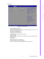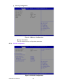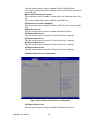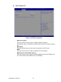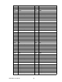
1
User Manual SOM-6896 Copyright The documentation and the software included with this product are copyrighted 2015 by Advantech Co., Ltd. All rights are reserved. Advantech Co., Ltd. reserves the right to make improvements in the products described in this manual at any time without notice. No part of this manual may be reproduced, copied, translated or transmitted in any form or by any means without the prior written permission of Advantech Co., Ltd. Information provided in this manual is intended to be accurate and reliable. However, Advantech Co., Ltd. assumes no responsibility for its use, nor for any infringements of the rights of third parties, which may result from its use. Acknowledgements Intel is a trademark of Intel Corporation. Microsoft Windows and MS-DOS are registered trademarks of Microsoft Corp. All other product names or trademarks are properties of their respective owners. Product Warranty (2 years) Advantech warrants to you, the original purchaser, that each of its products will be free from defects in materials and workmanship for two years from the date of purchase. This warranty does not apply to any products which have been repaired or altered by persons other than repair personnel authorized by Advantech, or which have been subject to misuse, abuse, accident or improper installation. Advantech assumes no liability under the terms of this warranty as a consequence of such events. Because of Advantech’s high quality-control standards and rigorous testing, most of our customers never need to use our repair service. If an Advantech product is defective, it will be repaired or replaced at no charge during the warranty period. For outof-warranty repairs, you will be billed according to the cost of replacement materials, service time and freight. Please consult your dealer for more details. If you think you have a defective product, follow these steps: 1. Collect all the information about the problem encountered. (For example, CPU speed, Advantech products used, other hardware and software used, etc.) Note anything abnormal and list any onscreen messages you get when the problem occurs. 2. Call your dealer and describe the problem. Please have your manual, product, and any helpful information readily available. 3. If your product is diagnosed as defective, obtain an RMA (return merchandize authorization) number from your dealer. This allows us to process your return more quickly. 4. Carefully pack the defective product, a fully-completed Repair and Replacement Order Card and a photocopy proof of purchase date (such as your sales receipt) in a shippable container. A product returned without proof of the purchase date is not eligible for warranty service. 5. Write the RMA number visibly on the outside of the package and ship it prepaid to your dealer. SOM-6896 User Manual Part No. 2006689600 Edition 1 Printed in Taiwan May 2015 ii Declaration of Conformity CE This product has passed the CE test for environmental specifications. Test conditions for passing included the equipment being operated within an industrial enclosure. In order to protect the product from being damaged by ESD (Electrostatic Discharge) and EMI leakage, we strongly recommend the use of CE-compliant industrial enclosure products. FCC Class B Note: This equipment has been tested and found to comply with the limits for a Class B digital device, pursuant to part 15 of the FCC Rules. These limits are designed to provide reasonable protection against harmful interference in a residential installation. This equipment generates, uses and can radiate radio frequency energy and, if not installed and used in accordance with the instructions, may cause harmful interference to radio communications. However, there is no guarantee that interference will not occur in a particular installation. If this equipment does cause harmful interference to radio or television reception, which can be determined by turning the equipment off and on, the user is encouraged to try to correct the interference by one or more of the following measures: Reorient or relocate the receiving antenna. Increase the separation between the equipment and receiver. Connect the equipment into an outlet on a circuit different from that to which the receiver is connected. Consult the dealer or an experienced radio/TV technician for help. FM This equipment has passed the FM certification. According to the National Fire Protection Association, work sites are classified into different classes, divisions and groups, based on hazard considerations. This equipment is compliant with the specifications of Class I, Division 2, Groups A, B, C and D indoor hazards. Technical Support and Assistance 1. 2. Visit the Advantech website at http://support.advantech.com where you can find the latest information about the product. Contact your distributor, sales representative, or Advantech's customer service center for technical support if you need additional assistance. Please have the following information ready before you call: – Product name and serial number – Description of your peripheral attachments – Description of your software (operating system, version, application software, etc.) – A complete description of the problem – The exact wording of any error messages iii SOM-6896 User Manual Warnings, Cautions and Notes Warning! Warnings indicate conditions, which if not observed, can cause personal injury! Caution! Cautions are included to help you avoid damaging hardware or losing data. e.g. There is a danger of a new battery exploding if it is incorrectly installed. Do not attempt to recharge, force open, or heat the battery. Replace the battery only with the same or equivalent type recommended by the manufacturer. Discard used batteries according to the manufacturer's instructions. Note! Notes provide optional additional information. Document Feedback To assist us in making improvements to this manual, we would welcome comments and constructive criticism. Please send all such - in writing to: [email protected] Packing List Before setting up the system, check that the items listed below are included and in good condition. If any item does not accord with the table, please contact your dealer immediately. SOM-6896 CPU module 1 x Heatspreader (1960069307N001) SOM-6896 User Manual iv Safety Instructions 1. 2. 3. Read these safety instructions carefully. Keep this User Manual for later reference. Disconnect this equipment from any AC outlet before cleaning. Use a damp cloth. Do not use liquid or spray detergents for cleaning. 4. For plug-in equipment, the power outlet socket must be located near the equipment and must be easily accessible. 5. Keep this equipment away from humidity. 6. Put this equipment on a reliable surface during installation. Dropping it or letting it fall may cause damage. 7. The openings on the enclosure are for air convection. Protect the equipment from overheating. DO NOT COVER THE OPENINGS. 8. Make sure the voltage of the power source is correct before connecting the equipment to the power outlet. 9. Position the power cord so that people cannot step on it. Do not place anything over the power cord. 10. All cautions and warnings on the equipment should be noted. 11. If the equipment is not used for a long time, disconnect it from the power source to avoid damage by transient overvoltage. 12. Never pour any liquid into an opening. This may cause fire or electrical shock. 13. Never open the equipment. For safety reasons, the equipment should be opened only by qualified service personnel. 14. If one of the following situations arises, get the equipment checked by service personnel: The power cord or plug is damaged. Liquid has penetrated into the equipment. The equipment has been exposed to moisture. The equipment does not work well, or you cannot get it to work according to the user's manual. The equipment has been dropped and damaged. The equipment has obvious signs of breakage. 15. DO NOT LEAVE THIS EQUIPMENT IN AN ENVIRONMENT WHERE THE STORAGE TEMPERATURE MAY GO BELOW -20° C (-4° F) OR ABOVE 60° C (140° F). THIS COULD DAMAGE THE EQUIPMENT. THE EQUIPMENT SHOULD BE IN A CONTROLLED ENVIRONMENT. 16. CAUTION: DANGER OF EXPLOSION IF BATTERY IS INCORRECTLY REPLACED. REPLACE ONLY WITH THE SAME OR EQUIVALENT TYPE RECOMMENDED BY THE MANUFACTURER, DISCARD USED BATTERIES ACCORDING TO THE MANUFACTURER'S INSTRUCTIONS. The sound pressure level at the operator's position according to IEC 704-1:1982 is no more than 70 dB (A). DISCLAIMER: This set of instructions is given according to IEC 704-1. Advantech disclaims all responsibility for the accuracy of any statements contained herein. v SOM-6896 User Manual Safety Precaution - Static Electricity Follow these simple precautions to protect yourself from harm and the products from damage. To avoid electrical shock, always disconnect the power from your PC chassis before you work on it. Don't touch any components on the CPU card or other cards while the PC is on. Disconnect power before making any configuration changes. The sudden rush of power as you connect a jumper or install a card may damage sensitive electronic components. SOM-6896 User Manual vi Contents Chapter Chapter 1 General Information ............................1 1.1 1.2 1.3 Introduction ............................................................................................... 2 Specifications ............................................................................................ 2 1.2.1 Board Information ......................................................................... 2 1.2.2 System Information ....................................................................... 2 1.2.3 Display .......................................................................................... 2 1.2.4 Expansion Interface ...................................................................... 3 1.2.5 I/O ................................................................................................. 3 1.2.6 iManager 2.0 ................................................................................. 3 1.2.7 Mechanical and Environmental Specification ............................... 3 Functional Block Diagram ......................................................................... 4 2 Mechanical Information ......................5 2.1 Board Information...................................................................................... 6 Figure 2.1 Board Chips Identify - Front........................................ 6 Figure 2.2 Board Chips Identify - Back ........................................ 6 Mechanical Drawing.................................................................................. 7 Figure 2.3 Board Mechanical Drawing - Front ............................. 7 Figure 2.4 Board Mechanical Drawing - Back ............................. 7 Assembly Drawing .................................................................................... 8 Figure 2.5 Assembly Drawing (For Reference Only) ................... 8 Figure 2.6 Heatspreader Pre-Assembly (For Reference Only).... 8 Assembly Drawing .................................................................................... 9 Figure 2.7 Main Chip Height and Tolerance (GT2)...................... 9 Figure 2.8 Main Chip Height and Tolerance (GT3)...................... 9 2.2 2.3 2.4 Chapter 3 AMI BIOS ............................................11 3.1 Introduction ............................................................................................. 12 Figure 3.1 BIOS Setup Utility Main Screen................................ 12 Entering Setup ........................................................................................ 13 3.2.1 Main Setup.................................................................................. 13 Figure 3.2 Main setup screen .................................................... 13 3.2.2 Advanced BIOS Features Setup................................................. 14 Figure 3.3 Advanced BIOS Features Setup Screen .................. 14 Figure 3.4 CPU Configuration.................................................... 15 Figure 3.5 Trusted Computing ................................................... 16 Figure 3.6 ACPI Settings ........................................................... 17 Figure 3.7 PCH-FW Configuration............................................. 18 Figure 3.8 Firmware Update Configuration................................ 19 Figure 3.9 W83627DHG Super IO Configuration ...................... 19 Figure 3.10Serial Port 0 Configuration ....................................... 20 Figure 3.11Serial Port 1 Configuration ....................................... 21 Figure 3.12Parallel Port Configuration........................................ 22 Figure 3.13iManager Configuration ............................................ 23 Figure 3.14Serial Port 2 Configuration ....................................... 24 Figure 3.15Serial Port 3 Configuration ....................................... 25 Figure 3.16Hardware Monitor ..................................................... 26 Figure 3.17Serial Port Console Redirection ............................... 27 Figure 3.18SATA Configuration.................................................. 28 Figure 3.19Network Stack Configuration .................................... 29 Figure 3.20CSM Configuration ................................................... 29 3.2 vii SOM-6896 User Manual 3.2.3 3.2.4 3.2.5 3.2.6 Chapter Figure 3.21USB Configuration.................................................... 30 Chipset........................................................................................ 32 Figure 3.22Chipset Setup........................................................... 32 Figure 3.23System Agent (SA) Configuration ............................ 33 Figure 3.24Graphics Configuration............................................. 34 Figure 3.25 LCD Control............................................................. 35 Figure 3.26Memory Configuration .............................................. 36 Figure 3.27PCH-IO Configuration .............................................. 36 Figure 3.28PCI Express Configuration ....................................... 37 Figure 3.29PCI Express Root Port 0 Configuration.................... 38 Figure 3.30PCI Express Root Port 1 Configuration.................... 39 Figure 3.31PCI Express Root Port 2 Configuration.................... 40 Figure 3.32PCI Express Root Port 3 Configuration.................... 41 Figure 3.33USB Configuration.................................................... 42 Figure 3.34PCH Azalia Configuration......................................... 43 Security Setting........................................................................... 44 Figure 3.35Security Setup .......................................................... 44 Boot Settings .............................................................................. 45 Figure 3.36Boot Setting.............................................................. 45 Save & Exit ................................................................................. 46 Figure 3.37Save & Exit............................................................... 46 4 S/W Introduction & Installation........ 49 4.1 4.2 4.3 S/W Introduction ..................................................................................... 50 Driver Installation .................................................................................... 50 4.2.1 Windows Driver Setup ................................................................ 50 4.2.2 Other OS..................................................................................... 50 Advantech iManager ............................................................................... 51 Appendix A Pin Assignment................................. 53 A.1 SOM-6896 Type 6 Pin Assignment......................................................... 54 Appendix B Watchdog Timer................................ 59 B.1 Programming the Watchdog Timer ......................................................... 60 Appendix C Programming GPIO........................... 61 C.1 GPIO Register......................................................................................... 62 Appendix D System Assignments........................ 63 D.1 System I/O Ports..................................................................................... 64 Table D.1: System I/O ports....................................................... 64 DMA Channel Assignments .................................................................... 65 Table D.2: DMA Channel Assignments ..................................... 65 Interrupt Assignments ............................................................................. 66 Table D.3: Interrupt Assignments .............................................. 66 1st MB Memory Map............................................................................... 67 Table D.4: 1st MB Memory Map ................................................ 67 D.2 D.3 D.4 SOM-6896 User Manual viii Chapter 1 1 General Information This chapter gives background information on the SOM-6896 CPU Computer on Module. Sections include: Introduction Specification Functional Block Diagram 1.1 Introduction SOM-6896 is a new COM Express (PICMG COM.0) R2.1 Compact Module in a Type 6 pin-out module board. SOM-6896 is equipped with the latest 5th generation Intel® Core™ Processor on a compact size 95x95mm COM Express module, resulting in low power consumption and excellent CPU and graphics performance. SOM-6896 is built for use in demanding applications such as medical equipment, automation, and gaming industries. Compared with its predecessor, SOM-6896 is designed with the latest 5th generation Intel® Core™ Processor and supports DirectX 11.1, OpenGL 4.2 and OpenCL 2.0, and AVC/VC1/MPEG2 codec support. SOM-6896 supports 3 simultaneous displays (VGA, LVDS, HDMI/DisplayPort/DVI), and HDMI supports up to 4K (4096x2304) @ 24Hz resolutions. SOM-6896 provides flexible IO interface options with up to 3 PCIe x1 to fulfill various function extension requirements. In addition, SOM-6896 improves thermal performance with an added mounting hole designed around the CPU with a stronger board structure that avoids board bending - designed to improve thermal effect, it offers excellent connection between the module board and thermal solution. 1.2 Specifications 1.2.1 Board Information Pin Definition: PICMG COM.0 R2.1 Type 6 pin-out definition Form Factor: PICMG COM.0 R2.1 Compact Module 95 x 95 mm 1.2.2 System Information CPU: 5th Gen Intel® Core™ / Celeron® Processors CPU+PCH Base Freq. Max Turbo Frequency Core Cache (MB) TDP(W) Intel® i7-5650U 2.2 GHz 3.1 GHz 2 4 15 Intel® i5-5350U 1.8 GHz 2.9 GHz 2 3 15 Intel® i3-5010U 2.1 GHz NA 2 3 15 Celeron® 3765U 1.9 GHz NA 2 2 15 Memory: 2 SODIMM Socket for DDR3L-1600, up to 16 GB BIOS: AMI UEFI BIOS 128 Mb Power management: Supports power saving modes including Normal / Standby / Suspend modes. ACPI 2.0 compliant 1.2.3 Display Graphic Core: Intel® HD Graphic supports DX11.1, OpenGL 4.0/4.2, OCL1.2, HW Decode/Encode for H.264/AVC, VC-1, SVC, MPEG2, Decode for VP8 CPU Graphics Core Base Freq. Max Freq. Intel® i7-5650U Intel® HD graphics 6000 300 MHz 1 GHz Intel® i5-5350U Intel® HD graphics 6000 300 MHz 1 GHz Intel® i3-5010U Intel® HD Graphics 5500 300 MHz 900 MHz Celeron® 3765U Intel® HD Graphics 300 MHz 850 MHz VGA: Resolution up to 1920 x 1200 SOM-6896 User Manual 2 1.2.4 Expansion Interface PCI Express x1: Supports 4 PCIe x1 compliant ports by default. x4 x2 x1 Default 0 0 4 Option 1 1 0 3 Audio Interface: Intel HD Audio interface LPC Bus: Yes (24 MHz) SMBus: Yes I2C Bus: up to 1 MB/s SPI: Supports SPI BIOS only 1.2.5 I/O Ethernet: Intel i218LM Gigabit LAN supports 10/100/1000 Mbps Speed SATA: Supports 4 ports, Gen3 (6Gb/s) and Gen2 (3Gb/s), RAID 0, 1, 5, 10 COM Port: 2 Ports (2-Wire) Express Card: Yes USB Interface: Supports 2 ports USB3.0, 8 ports USB 2.0 Panel Control: Supports panel backlight on/off control, brightness control Thermal Protection: Supports thermal shutdown or CPU throttling Watchdog Timer: 65536 level timer interval, from 0 ~ 65535 sec Smart Fan: 2 Ports; 1 Port on COM Module. Support 12V Fan, 1 Port on Carrier Board GPIO: 8-bit GPIO Power Supply Voltage: ATX (Vin 4.75-20V, Vsb 4.75-5.25V) TPM: TPM 1.2 (Optional) 1.2.6 iManager 2.0 Refer to section 4.3. 1.2.7 Mechanical and Environmental Specification Dimensions: 95 x 95 mm (3.74" x 3.74") Power Type and Supply Voltage: – ATX (Vin 4.75 - 20 V, Vsb 4.75 - 5.25 V) Power Requirement: – CPU SKU: Intel i7-5650U, Intel i5-5350U, Intel i3-5010U, 3765U (Celeron) – OS: Windows 7 3 SOM-6896 User Manual General Information LVDS: Single and dual channel 18/24-bit resolutions up to 1920 x 1200 DDI (HDMI/DVI/DisplayPort): – DDI 1: supports HDMI (1.4a specification compliant with 3D) resolutions up to 4096 x 2304, DisplayPort resolutions up to 3840 x 2160 DVI resolutions up to 1920 x 1200 (DDI 2: Optional) Dual Display: – LVDS (eDP) + HDMI (DDI1) – LVDS (eDP) + VGA (DDI2 DP) – LVDS (eDP)+ DP (DDI1) – HDMI (DDI1) + VGA (DDI2 DP) Triple Display: LVDS (eDP) + VGA (DDI2 DP) + HDMI (DDI1) Chapter 1 – Test software: Burn In Test V7.0Pro (1014) (CPU, RAM, 2D&3D Graphics and Disk with 100%), TAT version 5.0.1010 (CPU100% and Graphic 100%) – Idle: 5.267W (i3) – Max: 15.775W (i3) Temperature Specification: – Operating: 0 ~ 60° C (32 ~ 140° F) – Storage: -40 ~ 85° C (-40 ~ 185° F) Humidity Specification: – Operating: 40° C @ 95% relative humidity, non-condensing – Storage: 60° C @ 95% relative humidity, non-condensing 1.3 Functional Block Diagram VR12.6 Dual Channel DDR3L eDP 204pin SO-DIMM x 2 1333/1600MHz up to 16GB DDI Port 2 DP (Optional 1 PCIex4) Chrontel CH7511 Dual LVDS Channel Chrontel CH7517 Analog VGA 8 USB2.0 Connector Row C,D HD Audio 2 USB3.0 4 PCIex1 DDI Port 1 HDMI / DisplayPort / DVI 1 PCIex1 DDI Port 2 HDMI / DisplayPort / DVI Giga LAN Intel® I218LM Option with Analog VGA LPC BUS (24MHz) TPM1.2 WDT / GPIO / I2C iManager RS1/ RS2/ FAN SMBus - Optional function SOM-6896 User Manual SPI Bus SPI BIOS 4 Connector Row A,B 4 SATA3 5th Gen Intel® Core™ / Celeron® Processors U-Series (SoC) Chapter 2 2 Mechanical Information This chapter gives mechanical information on the SOM-6896 CPU Computer on Module. Sections include: Board Information Mechanical Drawing Assembly Drawing 2.1 Board Information The figures below indicate the main chips on SOM-6896 Computer-on-Module. Please aware of these positions while designing your own carrier board to avoid mechanical issues, as well as designing thermal solution contact points for best thermal dissipation performance. DDR3L SODIMMs Intel 5th Gen. SoC On-Module Smart FAN connector BIOS Socket Figure 2.1 Board Chips Identify - Front COM Express Connector Figure 2.2 Board Chips Identify - Back SOM-6896 User Manual 6 56.4 For more details about 2D/3D models, please look on the Advantech COM support service website http://com.advantech.com. 0 6.93 57.4 Mechanical Information 18.8 ø6 4.00 11.5 Figure 2.3 Board Mechanical Drawing - Front R2 ø6 91.00 91.00 83.5 18.00 6.00 0 91.00 95.00 78.5 15.00 20.8 0 4.00 Figure 2.4 Board Mechanical Drawing - Back 7 Chapter 2 2.2 Mechanical Drawing SOM-6896 User Manual 2.3 Assembly Drawing These figures demonstrate the assembly order from thermal module, COM module to carrier board. Figure 2.5 Assembly Drawing (For Reference Only) There are 4 reserved screw holes for SOM-6896 to be pre-assembled with heat spreader. Figure 2.6 Heatspreader Pre-Assembly (For Reference Only) SOM-6896 User Manual 8 Please consider the CPU and chip height tolerance when designing your thermal solution. Figure 2.7 Main Chip Height and Tolerance (GT2) *F5=NOM: 1.195 TOL:±0.089 (POST SMT STACKUP HEIGHT BASED ON LIMITED DATA FROM INTEL REFERENCE BOARD DESIGN) Figure 2.8 Main Chip Height and Tolerance (GT3) 9 SOM-6896 User Manual Mechanical Information *F5=NOM: 1.195 TOL:±0.089 (POST SMT STACKUP HEIGHT BASED ON LIMITED DATA FROM INTEL REFERENCE BOARD DESIGN) Chapter 2 2.4 Assembly Drawing SOM-6896 User Manual 10 Chapter 3 AMI BIOS Sections include: Introduction Entering Setup 3 3.1 Introduction AMI BIOS has been integrated into many motherboards for over a decade. With the AMI BIOS Setup program, users can modify BIOS settings and control various system features. This chapter describes the basic navigation of the BIOS Setup Utility. Figure 3.1 BIOS Setup Utility Main Screen AMI's BIOS ROM has a built-in Setup program that allows users to modify the basic system configuration. This information is stored in flash ROM so it retains the Setup information when the power is turned off. SOM-6896 User Manual 12 Turn on the computer and then press <ESC> or <DEL> to enter Setup menu. 3.2.1 Main Setup When users first enter the BIOS Setup Utility, users will enter the Main setup screen. Users can always return to the Main setup screen by selecting the Main tab. There are two Main Setup options. They are described in this section. The Main BIOS Setup screen is shown below. Chapter 3 3.2 Entering Setup AMI BIOS Figure 3.2 Main setup screen The Main BIOS setup screen has two main frames. The left frame displays all the options that can be configured. Grayed-out options cannot be configured; options in blue can. The right frame displays the key legend. Above the key legend is an area reserved for a text message. When an option is selected in the left frame, it is highlighted in white. Often a text message will accompany it. System time / System date Use this option to change the system time and date. Highlight System Time or System Date using the <Arrow> keys. Enter new values through the keyboard. Press the <Tab> key or the <Arrow> keys to move between fields. The date must be entered in MM/DD/YY format. The time must be entered in HH:MM:SS format. 13 SOM-6896 User Manual 3.2.2 Advanced BIOS Features Setup Select the Advanced tab from the SOM-6896 setup screen to enter the Advanced BIOS Setup screen. Users can select any item in the left frame of the screen, such as CPU Configuration, to go to the sub menu for that item. Users can display an Advanced BIOS Setup option by highlighting it using the <Arrow> keys. All Advanced BIOS Setup options are described in this section. The Advanced BIOS Setup screens are shown below. The sub menus are described on the following pages. Figure 3.3 Advanced BIOS Features Setup Screen SOM-6896 User Manual 14 Chapter 3 3.2.2.1 CPU Configuration AMI BIOS Figure 3.4 CPU Configuration Hyper-threading This item allows users to enable for Windows XP and Linux (OS optimized for Hyper-Threading Technology) and Disable for other OS (OS not optimized for Hyper-Threading Technology) When Disable only one thread per enabled core is enabled. Active Processor Cores Number of cores to enable in each processor package. Limit CPUID Maximum This item disable for Windows XP. Execute Disable Bit XD can prevent certain classes of malicious buffer overflow attacks when combined with a supporting OS (Windows Server 2003 SP1, Windows XP SP2, SuSE Linux 9.2, RedHat Enterprise 3 update 3.) Intel Virtualization Technology When enabled, a VMM can utilize the additional hardware capabilities provided by Vanderpool Technology. Hardware Prefetcher Enable the Mid Level Cache (L2) streamer prefetcher. Adjacent Cache Line Prefetch Enable the Mid Level Cache (L2) prefetching of adjacent cache lines. CPU AES Enable/Disable CPU Advanced Encryption Standard instructions. Boot performance mode Select the performance state that the BIOS will set before OS handoff. EIST 15 SOM-6896 User Manual Enable/Disable Intel SpeedStep. CPU C States Enable of disable CPU C states. ACPI CTDP BIOS Enable/Disable ACPI CTDP BIOS Support. Configurable TDP Allow reconfiguration of TDP levels base on current power and thermal delivery capabilities of the system. Config TDP LOCK Lock the Config TDP Control register. 3.2.2.2 Trusted Computing Figure 3.5 Trusted Computing Security Device Support Enables or Disables BIOS support for security device. O.S. will not show security Device. TCG EFI protocol and INT1A interface will not be available. SOM-6896 User Manual 16 Chapter 3 3.2.2.3 ACPI Settings AMI BIOS Figure 3.6 ACPI Settings Enable ACPI Auto Configuration Enables or Disables BIOS ACPI Auto Configuration. Enable Hibernation Enables or Disables System ability to Hibernate (OS/S4 Sleep State). This option may be not effective with some OS. ACPI Sleep State Select the highest ACPI sleep state the system will enter when the SUSPEND button is pressed. Lock Legacy Resources Enables or Disables Lock of Legacy Resources S3 Video Repost Enable or Disable S3 Video Repost ACPI Low Power S0 Idle Enable or Disable ACPI Low Power S0 Idle Support. 17 SOM-6896 User Manual 3.2.2.4 PCH-FW Configuration Figure 3.7 PCH-FW Configuration ME Unconfig on RTC Clear State Enable/Disable ME firmware un-configuration on RTC clear State. fTPM Switch Selection Selects the desired fTPM solution to be used. TPM Device Selection Selects TPM device: PTT or dTPM. PTT-Enable PTT in SkuMgr dTPM 1.2 - Disables PTT in SkuMgr Warning! PTT/dTPM will be disabled and all data saved on it will be lost. Firmware Update Configuration Configure Management Engine Technology Parameters. SOM-6896 User Manual 18 Chapter 3 3.2.2.5 Firmware Update Configuration AMI BIOS Figure 3.8 Firmware Update Configuration ME FW Image Re-Flash Enable/Disable Me FW Image Re-Flash function. 3.2.2.6 W83627DHG Super IO Configuration Figure 3.9 W83627DHG Super IO Configuration 19 SOM-6896 User Manual Serial Port 0 Configuration Set Parameters of Serial Port 0 (COMA) Serial Port 1 Configuration Set Parameters of Serial Port 1 (COMB) Parallel Port Configuration Set Parameters of Parallel Port (LPT/LPTE) Serial Port 0 Configuration Figure 3.10 Serial Port 0 Configuration – Serial Port Enable or Disable Serial Port (COM) – Change Settings Select an optimal setting for Super IO device. SOM-6896 User Manual 20 Serial Port 1 Configuration Chapter 3 AMI BIOS Figure 3.11 Serial Port 1 Configuration – Serial Port Enable or Disable Serial Port (COM) – Change Settings Select an optimal setting for Super IO device. 21 SOM-6896 User Manual Parallel Port Configuration Figure 3.12 Parallel Port Configuration – Parallel Port Enable or Disable Parallel Port (LPT/LPTE) – Change Settings Select an optimal setting for Super IO device. – Device Mode Change the Printer Port mode. SOM-6896 User Manual 22 Chapter 3 3.2.2.7 iManager Configuration AMI BIOS Figure 3.13 iManager Configuration CPU Shutdown Temperature Enable/Disable CPU Shutdown Temperature. iManager Smart Fan - COM Module Control iManager Smart FAN function iManager Smart Fan - Carrier Board Control iManager Smart FAN Carrier Board function. Backlight Enable Polarity Switch Backlight Enable Polarity for Native or Invert Power Saving Mode Select Ite8528 Power Saving Mode Serial Port 2 Configuration Set Parameters of Serial Port 2 (COMA) Serial Port 3 Configuration Set Parameters of Serial Port 3 (COMB) Hardware Monitor Monitor hardware status 23 SOM-6896 User Manual Serial Port 2 Configuration Figure 3.14 Serial Port 2 Configuration – Serial Port Enable or Disable Serial Port (COM) – Change Settings Select an optimal setting for Super IO device. SOM-6896 User Manual 24 Serial Port 3 Configuration Chapter 3 AMI BIOS Figure 3.15 Serial Port 3 Configuration – Serial Port Enable or Disable Serial Port (COM) – Change Settings Select an optimal setting for Super IO device. 25 SOM-6896 User Manual Hardware Monitor Figure 3.16 Hardware Monitor – Hardware Monitor Information This item shows Hardware information parameters. SOM-6896 User Manual 26 Chapter 3 3.2.2.8 Serial Port Console Redirection AMI BIOS Figure 3.17 Serial Port Console Redirection COM0 Console Redirection Console Redirection Enable or Disable Serial Port for Out-of-Band Management / Windows Emergency Management Service (EMS) Console Redirection Console Redirection Enable or Disable 27 SOM-6896 User Manual 3.2.2.9 SATA Configuration Figure 3.18 SATA Configuration SATA Controller(s) Enable or disable SATA Device SATA Mode Selection Determines how SATA controller(s) operate Aggressive LPM Support Enable PCH to aggressively enter link power state. SATA Controller Speed Indicates the maximum speed the SATA controller can support. Port 0 Enable or Disable SATA port Hot Plug Designates this port as Hot Pluggable Port 1 Enable or Disable SATA port Hot Plug Designates this port as Hot Pluggable Port 2 Enable or Disable SATA port Hot Plug Designates this port as Hot Pluggable Port 3 Enable or Disable SATA port Hot Plug Designates this port as Hot Pluggable SOM-6896 User Manual 28 Chapter 3 3.2.2.10 Network Stack Configuration AMI BIOS Figure 3.19 Network Stack Configuration Network Stack Enable/Disable UEFI Network Stack 3.2.2.11 CSM Configuration Figure 3.20 CSM Configuration 29 SOM-6896 User Manual CSM Support Enable/Disable CSM Support GateA20 Active UPON Request- GA20 can be disabled using BIOS services. Always - do not allow disabling GA20; this option is useful when any RT code is executed above 1MB. Option ROM Messages Set display mode for Option ROM Boot option filter This option controls Legacy/UEFI ROMs priority. Network Controls the execution of UEFI and Legacy PXE OpROM Storage Controls the execution of UEFI and Legacy Storage OpROM Video Controls the execution of UEFI and Legacy Video OpROM Other PCI devices Determines OpROM execution policy for devices other than Network, Storage, or Video. 3.2.2.12 USB Configuration Figure 3.21 USB Configuration Legacy USB Support Enables Legacy USB support. Auto option disables legacy support if no USB devices are connected. Disable option will keep USB devices available only for EFI applications. XHCI Hand-off SOM-6896 User Manual 30 31 SOM-6896 User Manual AMI BIOS Chapter 3 This is a workaround for OS without XHCI ownership change should be claimed by XHCI driver. EHCI Hand-off This is a workaround for OS without EHCI hand-off support. The EHCI ownership change should be claimed by EHCI driver. USB Mass Storage Driver Support Enable/Disable USB Mass Storage Driver Support. USB transfer time-out The time-out value for Control, Bulk, and Interrupt transfers. Device reset time-out USB mass storage device Start Unit command time-out. Device power-up delay Maximum time the device will take before it properly reports itself to the Host Controller. 'Auto' uses default value: for a Root port the delay is taken from Hub descriptor. 3.2.3 Chipset Select the Chipset tab from the SOM-6896 setup screen to enter the Chipset BIOS Setup screen. You can display a Chipset BIOS Setup option by highlighting it using the <Arrow> keys. All Plug and Play BIOS Setup options are described in this section. The Plug and Play BIOS Setup screen is shown below. Figure 3.22 Chipset Setup System Agent (SA) Configuration This item allows users to change System Agent (SA) Parameters. PCH-IO Configuration This item allows users to change PCH Parameters. SOM-6896 User Manual 32 Chapter 3 3.2.3.1 System Agent (SA) Configuration AMI BIOS Figure 3.23 System Agent (SA) Configuration VT-d Check to enable VT-d function on MCH. CHAP Device (B0:D7:F0) Enable or disable SA Chap Device Thermal Device (B0:D4:F0) Enable or disable SA Thermal Device CPU SA Audio Device (B0:D3:F0) Enable or disable CPU SA Audio Device Graphics Configuration Config Graphics Settings Memory Configuration Memory Configuration Parameters 33 SOM-6896 User Manual Graphics Configuration Figure 3.24 Graphics Configuration – Graphics Turbo IMON Current Graphics turbo IMON current values supported (14-31) – Primary Display Selects which IGFX/PEG/PCI Graphics Device should be Primary Display or select SG for Switchable Gfx. – Internal Graphics Keeps IGD enabled based on the setup options. – GTT Size Selects the GTT Size – Aperture Size Selects the Aperture Size. Note: Above 4GB MMIO BIOS assignment is automatically enabled when selecting 2048 aperture. To use this feature, please disable CSM support – DVMT Pre-Allocated Selects DVMT 5.0 Pre-Allocated (Fixed) Graphics Memory size used by the Internal Graphics Device. – DVMT Total Gfx Mem Selects DVMT5.0 Total Graphic Memory size used by the Internal Graphics Device. – Gfx Low Power Mode This option is applicable for SFF only. – LCD Control This item allows customer to do LCD control. SOM-6896 User Manual 34 Chapter 3 LCD Control AMI BIOS Figure 3.25 LCD Control Primary IGFX Boot Display Selects the Video Device which will be activated during POST. This has no effect if external graphics present. DDI1(EFP) for HDMI/DP/DVI. LVDS (LFP) by Chrontel CH7511. VGA (EFP2) DP to VGA by Chrontel CH7517. LCD Panel Type Selects LCD panel used by Internal Graphics Device by selecting the appropriate setup item. Active LFP Selects the Active LFP Configuration. No LVDS: VBIOS does not enable LVDS. eDP Port-A: LFP Driver by Int-DisplayPort encoder from Port-A 35 SOM-6896 User Manual Memory Configuration Figure 3.26 Memory Configuration – Memory Information This item shows memory configuration parameters. 3.2.3.2 PCH-IO Configuration Figure 3.27 PCH-IO Configuration SOM-6896 User Manual 36 PCI Express Configuration Figure 3.28 PCI Express Configuration – PCI Express Clock Gating This item allows users to enable or disable PCI Express Clock Gating for each root port. – DMI Link ASPM Control 37 SOM-6896 User Manual AMI BIOS PCI Express Configuration This item allows users to change PCI Express Configuration settings. USB Configuration This item allows users to change USB Configuration settings. PCH Azalia Configuration This item allows users to change PCH Azalia Configuration settings. PCH LAN Controller Enable or disable onboard NIC. LAN PHY Drives GPI027 Enable/Disables LAN Phy driving GPI027 else platform drivers GPI027. Wake on LAN Enable or disable integrated LAN to wake the system. (The Wake on LAN cannot be disabled if ME is on at Sx state.) SLP_LAN# Low on DC Power Enable or disable SLP_LAN# Low on DC Power. SLP_S4 Assertion Width Select a minimum assertion width of the SLP_S4# signal. Restore AC Power Loss Select AC power state when power is re-applied after a power failure. Chapter 3 – – – – – – – This item allows users to enable or disable DMI Link ASPM Control. The Control of Active State Power Management on both NB side and SB side of the DMI Link. DMI Link Extended Synch Control This item allows users to enable or disable DMI Link Extended Synch Control. The Control of Extended Synch on SB side of the DMI Link. PCIE Root Port Function Swapping This item allows users to enable or disable PCIE Root Port Function Swapping. Subtractive Decode This item allows users to enable or disable Subtractive Decode. PCI Express Root Port 0 This item allows users to change PCI Express Root Port 0 settings. PCI Express Root Port 1 This item allows users to change PCI Express Root Port 1 settings. PCI Express Root Port 2 This item allows users to change PCI Express Root Port 2 settings. PCI Express Root Port 4 This item allows users to change PCI Express Root Port 4 settings. – PCI Express Root Port 0 Configuration Figure 3.29 PCI Express Root Port 0 Configuration PCI Express Root Port 0 This item allows users to enable or disable PCI Express Root Port. SOM-6896 User Manual 38 AMI BIOS – PCI Express Root Port 1 Configuration Figure 3.30 PCI Express Root Port 1 Configuration PCI Express Root Port 1 This item allows users to enable or disable PCI Express Root Port. ASPM This item allows users to select PCI Express Active State Power Management settings. PCIe Speed This item allows users to select PCIe Speed. Detect Non-Compliance Device Detect Non-Compliance Device PCI Express Device. If enable, it will take more time at POST time. 39 Chapter 3 ASPM This item allows users to select PCI Express Active State Power Management settings. PCIe Speed This item allows users to select PCIe Speed. Detect Non-Compliance Device Detect Non-Compliance Device PCI Express Device. If enable, it will take more time at POST time. SOM-6896 User Manual – PCI Express Root Port 2 Configuration Figure 3.31 PCI Express Root Port 2 Configuration PCI Express Root Port 2 This item allows users to enable or disable PCI Express Root Port. ASPM This item allows users to select PCI Express Active State Power Management settings. PCIe Speed This item allows users to select PCIe Speed. Detect Non-Compliance Device Detect Non-Compliance Device PCI Express Device. If enable, it will take more time at POST time. SOM-6896 User Manual 40 Chapter 3 – PCI Express Root Port 3 Configuration AMI BIOS Figure 3.32 PCI Express Root Port 3 Configuration PCI Express Root Port 3 This item allows users to enable or disable PCI Express Root Port. ASPM This item allows users to select PCI Express Active State Power Management settings. PCIe Speed This item allows users to select PCIe Speed. Detect Non-Compliance Device Detect Non-Compliance Device PCI Express Device. If enable, it will take more time at POST time. 41 SOM-6896 User Manual USB Configuration Figure 3.33 USB Configuration – USB Precondition This item allows users to enable or disable USB Precondition. Precondition work on USB host controller and root ports for faster enumeration. – XHCI Mode This item allows users to select mode of operation of XHCI mode. – BTCG This item allows users to enable or disable trunk clock gating. – USB Ports Per-Port Disable Control This item allows users to enable or disable USB Ports Per-Port Disable Control. Control each of the USB ports (0~13) disabling SOM-6896 User Manual 42 PCH Azalia Configuration Chapter 3 AMI BIOS Figure 3.34 PCH Azalia Configuration – Azalia Control Detection of the Azalia device. Disable- Azalia will be unconditionally disabled Enable- Azalia will be unconditionally Enabled Auto- Azalia will be enabled if present, disabled otherwise. – Azalia Docking Support Enable or disable Azalia Docking Support of Audio Controller – Azalia PME Enable or disable Power Management capability of Audio Controller. 43 SOM-6896 User Manual 3.2.4 Security Setting Figure 3.35 Security Setup Select Security Setup from the SOM-6896 Setup main BIOS setup menu. All Security Setup options, such as password protection is described in this section. To access the sub menu for the following items, select the item and press <Enter>: Change Administrator / User Password: Select this option and press <ENTER> to access the sub menu, and then type in the password. SOM-6896 User Manual 44 Chapter 3 3.2.5 Boot Settings AMI BIOS Figure 3.36 Boot Setting Setup Prompt Timeout This item allows users to select the number of seconds to wait for setup activation key. Bootup NumLock State Select the keyboard NumLock state. Quiet Boot This item allows users to enable or disable Quiet Boot option. Fast Boot This item allows users to enable or disable boot with initialization of a minimal set of devices required to launch active boot option. It has no effect for BBS boot options. 45 SOM-6896 User Manual 3.2.6 Save & Exit Figure 3.37 Save & Exit 3.2.6.1 Save Changes and Exit When users have completed system configuration, select this option to save changes, exit BIOS setup menu and reboot the computer if necessary to take effect all system configuration parameters. 3.2.6.2 Discard Changes and Exit Select this option to quit Setup without making any permanent changes to the system configuration. 3.2.6.3 Save Changes and Reset When users have completed system configuration, select this option to save changes, exit BIOS setup menu and reboot the computer to take effect all system configuration parameters. 3.2.6.4 Discard Changes and Reset Select this option to quit Setup without making any permanent changes to the system configuration and reboot the computer. 3.2.6.5 Save Changes When users have completed system configuration, select this option to save changes without exit BIOS setup menu. 3.2.6.6 Discard Changes Select this option to discard any current changes and load previous system configuration. SOM-6896 User Manual 46 3.2.6.9 Restore User Defaults The users can select this option to restore user defaults. 3.2.6.10 Launch EFI Shell from file system device This item attempts to Launch EFI Shell application (Shell.efi) from one of the available file system devices. 47 SOM-6896 User Manual AMI BIOS 3.2.6.8 Save User Defaults When users have completed system configuration, select this option to save changes as user defaults without exit BIOS setup menu. Chapter 3 3.2.6.7 Restore Defaults The SOM-6896 automatically configures all setup items to optimal settings when users select this option. Optimal Defaults are designed for maximum system performance, but may not work best for all computer applications. In particular, do not use the Optimal Defaults if the user's computer is experiencing system configuration problems. SOM-6896 User Manual 48 Chapter 4 4 S/W Introduction & Installation Sections include: S/W Introduction Driver Installation Advantech iManager 4.1 S/W Introduction The mission of Advantech Embedded Software Services is to "Enhance quality of life with Advantech platforms and Microsoft Windows embedded technology." We enable Windows Embedded software products on Advantech platforms to more effectively support the embedded computing community. Customers are freed from the hassle of dealing with multiple vendors (Hardware suppliers, System integrators, Embedded OS distributor) for projects. Our goal is to make Windows Embedded Software solutions easily and widely available to the embedded computing community. 4.2 Driver Installation The Intel Chipset Software Installation (CSI) utility installs the Windows INF files that outline to the operating system how the chipset components will be configured. 4.2.1 Windows Driver Setup To install the drivers on a windows-based OS, please connect to the internet and go to http://support.advantech.com.tw to download the drivers that you want to install and follow Driver Setup instructions to complete the installation. 4.2.2 Other OS To install the drivers for Linux or other OS, please connect to the internet and go to http://support.advantech.com.tw to download the setup file. SOM-6896 User Manual 50 51 SOM-6896 User Manual S/W Introduction & Installation Advantech's platforms come equipped with iManager, a micro controller that provides embedded features for system integrators. Embedded features have been moved from the OS/BIOS level to the board level, to increase reliability and simplify integration. iManager runs whether the operating system is running or not; it can count the boot times and running hours of the device, monitor device health, and provide an advanced watchdog to handle errors as they happen. iManager also comes with a secure & encrypted EEPROM for storing important security keys or other customer information. All the embedded functions are configured through the API and provide corresponding utilities to demonstrate. These APIs comply with PICMG EAPI (Embedded Application Programmable Interface) specifications and makes these embedded features easier to integrate, speed development schedules, and provide customer's with software continuity while upgrading hardware. More details of how to use the APIs and utilities, please refer to the Advantech iManager 2.0 Software API User Manual. Chapter 4 4.3 Advantech iManager SOM-6896 User Manual 52 Appendix A A Pin Assignment This appendix gives you the information about the hardware pin assignment of the SOM-6896 CPU System on Module. Sections include: SOM-6896 Type 6 Pin Assignment A.1 SOM-6896 Type 6 Pin Assignment This section gives SOM-6896 pin assignment on COM Express connector which compliant with COMR.0 R2.1 Type 6 pin-out definitions. More details about how to use these pins and get design reference, please contact to Advantech for design guide, checklist, reference schematic, and other hardware/software supports. SOM-6896 Row A,B A1 GND (FIXED) B1 GND (FIXED) A2 GBE0_MDI3- B2 GBE0_ACT# A3 GBE0_MDI3+ B3 LPC_FRAME# A4 GBE0_LINK100# B4 LPC_AD0 A5 GBE0_LINK1000# B5 LPC_AD1 A6 GBE0_MDI2- B6 LPC_AD2 A7 GBE0_MDI2+ B7 LPC_AD3 A8 GBE0_LINK# B8 N/A A9 GBE0_MDI1- B9 N/A A10 GBE0_MDI1+ B10 LPC_CLK A11 GND (FIXED) B11 GND (FIXED) A12 GBE0_MDI0- B12 PWRBTN# A13 GBE0_MDI0+ B13 SMB_CK A14 N/A B14 SMB_DAT A15 SUS_S3# B15 SMB_ALERT# A16 SATA0_TX+ B16 SATA1_TX+ A17 SATA0_TX- B17 SATA1_TX- A18 SUS_S4# B18 SUS_STAT# A19 SATA0_RX+ B19 SATA1_RX+ A20 SATA0_RX- B20 SATA1_RX- A21 GND (FIXED) B21 GND (FIXED) A22 SATA2_TX+ B22 SATA3_TX+ A23 SATA2_TX- B23 SATA3_TX- A24 SUS_S5# B24 PWR_OK A25 SATA2_RX+ B25 SATA3_RX+ A26 SATA2_RX- B26 SATA3_RX- A27 BATLOW# B27 WDT A28 (S)ATA_ACT# B28 AC/HDA_SDIN2 A29 AC/HDA_SYNC B29 AC/HDA_SDIN1 A30 AC/HDA_RST# B30 AC/HDA_SDIN0 A31 GND (FIXED) B31 GND (FIXED) A32 AC/HDA_BITCLK B32 SPKR A33 AC/HDA_SDOUT B33 I2C_CK A34 BIOS_DIS0# B34 I2C_DAT A35 THRMTRIP# B35 THRM# A36 USB6- B36 USB7- A37 USB6+ B37 USB7+ A38 USB_6_7_OC# B38 USB_4_5_OC# A39 USB4- B39 USB5- A40 USB4+ B40 USB5+ A41 GND (FIXED) B41 GND (FIXED) SOM-6896 User Manual 54 USB2- B42 USB3- A43 USB2+ B43 USB3+ A44 USB_2_3_OC# B44 USB_0_1_OC# A45 USB0- B45 USB1- A46 USB0+ B46 USB1+ A47 VCC_RTC B47 EXCD1_PERST# A48 EXCD0_PERST# B48 EXCD1_CPPE# A49 EXCD0_CPPE# B49 SYS_RESET# A50 LPC_SERIRQ B50 CB_RESET# A51 GND (FIXED) B51 GND (FIXED) A52 PCIE_TX5+ B52 PCIE_RX5+ A53 PCIE_TX5- B53 PCIE_RX5- A54 GPI0 B54 GPO1 A55 PCIE_TX4+ B55 PCIE_RX4+ A56 PCIE_TX4- B56 PCIE_RX4- A57 GND B57 GPO2 A58 PCIE_TX3+ (if C25 stuffed) B58 PCIE_RX3+ (if R545 stuffed) A59 PCIE_TX3- (if C24 stuffed) B59 PCIE_RX3- (if R546 stuffed) A60 GND (FIXED) B60 GND (FIXED) A61 PCIE_TX2+ B61 PCIE_RX2+ A62 PCIE_TX2- B62 PCIE_RX2- A63 GPI1 B63 GPO3 A64 PCIE_TX1+ B64 PCIE_RX1+ A65 PCIE_TX1- B65 PCIE_RX1- A66 GND B66 WAKE0# A67 GPI2 B67 WAKE1# A68 PCIE_TX0+ B68 PCIE_RX0+ A69 PCIE_TX0- B69 PCIE_RX0- A70 GND (FIXED) B70 GND (FIXED) A71 LVDS_A0+ B71 LVDS_B0+ A72 LVDS_A0- B72 LVDS_B0- A73 LVDS_A1+ B73 LVDS_B1+ A74 LVDS_A1- B74 LVDS_B1- A75 LVDS_A2+ B75 LVDS_B2+ A76 LVDS_A2- B76 LVDS_B2- A77 LVDS_VDD_EN B77 LVDS_B3+ A78 LVDS_A3+ B78 LVDS_B3- A79 LVDS_A3- B79 LVDS_BKLT_EN A80 GND (FIXED) B80 GND (FIXED) A81 LVDS_A_CK+ B81 LVDS_B_CK+ A82 LVDS_A_CK- B82 LVDS_B_CK- A83 LVDS_I2C_CK B83 LVDS_BKLT_CTRL A84 LVDS_I2C_DAT B84 VCC_5V_SBY A85 GPI3 B85 VCC_5V_SBY A86 RSVD(KBD_RST# if R472 stuffed) B86 VCC_5V_SBY A87 N/A B87 VCC_5V_SBY A88 PCIE_CLK_REF+ B88 BIOS_DIS1# A89 PCIE_CLK_REF- B89 VGA_RED 55 SOM-6896 User Manual Appendix A Pin Assignment A42 A90 GND (FIXED) B90 GND (FIXED) A91 SPI_POWER B91 VGA_GRN A92 SPI_MISO B92 VGA_BLU A93 GPO0 B93 VGA_HSYNC A94 SPI_CLK B94 VGA_VSYNC A95 SPI_MOSI B95 VGA_I2C_CK A96 N/A B96 VGA_I2C_DAT A97 TYPE10# B97 SPI_CS# A98 SER0_TX B98 RSVD A99 SER0_RX B99 RSVD A100 GND (FIXED) B100 GND (FIXED) A101 SER1_TX B101 FAN_PWMOUT A102 SER1_RX B102 FAN_TACHIN A103 LID# B103 SLEEP# A104 VCC_12V B104 VCC_12V A105 VCC_12V B105 VCC_12V A106 VCC_12V B106 VCC_12V A107 VCC_12V B107 VCC_12V A108 VCC_12V B108 VCC_12V A109 VCC_12V B109 VCC_12V A110 GND (FIXED) B110 GND (FIXED) SOM-6896 Row C,D C1 GND (FIXED) D1 GND (FIXED) C2 GND D2 GND C3 USB_SSRX0- D3 USB_SSTX0- C4 USB_SSRX0+ D4 USB_SSTX0+ C5 GND D5 GND C6 USB_SSRX1- D6 USB_SSTX1- C7 USB_SSRX1+ D7 USB_SSTX1+ C8 GND D8 GND C9 N/A D9 N/A C10 N/A D10 N/A C11 GND (FIXED) D11 GND (FIXED) C12 N/A D12 N/A C13 N/A D13 N/A C14 GND D14 GND C15 N/A D15 DDI1_CTRLCLK_AUX+ C16 N/A D16 DDI1_CTRLDATA_AUX- C17 RSVD D17 RSVD C18 RSVD D18 RSVD C19 N/A D19 N/A C20 N/A D20 N/A C21 GND (FIXED) D21 GND (FIXED) C22 N/A D22 N/A C23 N/A D23 N/A C24 DDI1_HPD D24 RSVD C25 N/A D25 RSVD SOM-6896 User Manual 56 N/A D26 DDI1_PAIR0+ C27 RSVD D27 DDI1_PAIR0- C28 RSVD D28 RSVD C29 N/A D29 DDI1_PAIR1+ C30 N/A D30 DDI1_PAIR1- C31 GND (FIXED) D31 GND (FIXED) C32 DDI2_CTRLCLK_AUX+ (if R108 stuffed) D32 DDI1_PAIR2+ C33 DDI2_CTRLDATA_AUX(if R109 stuffed) D33 DDI1_PAIR2- C34 DDI2_DDC_AUX_SEL (if R108/R109 stuffed) D34 DDI1_DDC_AUX_SEL C35 RSVD D35 RSVD C36 N/A D36 DDI1_PAIR3+ C37 N/A D37 DDI1_PAIR3- C38 N/A D38 RSVD C39 N/A D39 DDI2_PAIR0+ (if R6 stuffed) C40 N/A D40 DDI2_PAIR0- (if R5 stuffed) C41 GND (FIXED) D41 GND (FIXED) C42 N/A D42 DDI2_PAIR1+ (if R8 stuffed) C43 N/A D43 DDI2_PAIR1- (if R7 stuffed) C44 N/A D44 DDI2_HPD (if R544 stuffed) C45 RSVD D45 RSVD C46 N/A D46 DDI2_PAIR2+ (if R5/R6/R7/R8 stuffed) C47 N/A D47 DDI2_PAIR2(if R5/R6/R7/R8 stuffed) C48 RSVD D48 RSVD C49 N/A D49 DDI2_PAIR3+ (if R5/R6/R7/R8 stuffed) C50 N/A D50 DDI2_PAIR3(if R5/R6/R7/R8 stuffed) C51 GND (FIXED) D51 GND (FIXED) C52 PCIE_RX16+ (if R140 stuffed) D52 PCIE_TX16+ (if C13 stuffed) C53 PCIE_RX16(if R139 stuffed) D53 PCIE_TX16- (if C12 stuffed) C54 TYPE0# D54 N/A C55 PCIE_RX17+ (if R140/R139 stuffed) D55 PCIE_TX17+ (if C13/C12 stuffed) C56 PCIE_RX17- (if R140/R139 stuffed) D56 PCIE_TX17- (if C13/C12 stuffed) C57 TYPE1# D57 TYPE2# C58 PCIE_RX18+ (if R140/R139 stuffed) D58 PCIE_TX18+ (if C13/C12 stuffed) C59 PCIE_RX18(if R140/R139 stuffed) D59 PCIE_TX18(if C13/C12 stuffed) C60 GND (FIXED) D60 GND (FIXED) C61 PCIE_RX19+ (if R140/R139 stuffed) D61 PCIE_TX19+ (if C13/C12 stuffed) C62 PCIE_RX19(if R140/R139 stuffed) D62 PCIE_TX19(if C13/C12 stuffed) C63 RSVD D63 RSVD 57 SOM-6896 User Manual Appendix A Pin Assignment C26 C64 RSVD D64 RSVD C65 N/A D65 N/A C66 N/A D66 N/A C67 RSVD D67 GND C68 N/A D68 N/A C69 N/A D69 N/A C70 GND (FIXED) D70 GND (FIXED) C71 N/A D71 N/A C72 N/A D72 N/A C73 GND D73 GND C74 N/A D74 N/A C75 N/A D75 N/A C76 GND D76 GND C77 RSVD D77 RSVD C78 N/A D78 N/A C79 N/A D79 N/A C80 GND (FIXED) D80 GND (FIXED) C81 N/A D81 N/A C82 N/A D82 N/A C83 RSVD D83 RSVD C84 GND D84 GND C85 N/A D85 N/A C86 N/A D86 N/A C87 GND D87 GND C88 N/A D88 N/A C89 N/A D89 N/A C90 GND (FIXED) D90 GND (FIXED) C91 N/A D91 N/A C92 N/A D92 N/A C93 GND D93 GND C94 N/A D94 N/A C95 N/A D95 N/A C96 GND D96 GND C97 RSVD D97 N/A C98 N/A D98 N/A C99 N/A D99 N/A C100 GND (FIXED) D100 GND (FIXED) C101 N/A D101 N/A C102 N/A D102 N/A C103 GND D103 GND C104 VCC_12V D104 VCC_12V C105 VCC_12V D105 VCC_12V C106 VCC_12V D106 VCC_12V C107 VCC_12V D107 VCC_12V C108 VCC_12V D108 VCC_12V C109 VCC_12V D109 VCC_12V C110 GND (FIXED) D110 GND (FIXED) SOM-6896 User Manual 58 Appendix B B Watchdog Timer This appendix gives you the information about the watchdog timer programming on the SOM-6896 CPU System on Module. Sections include: Watchdog Timer Programming B.1 Programming the Watchdog Timer Trigger Event Note IRQ IRQ5, 7, 14 (BIOS setting default disable)** NMI N/A SCI Power button event Power Off Support H/W Restart Support WDT Pin Activate Support ** WDT new driver support automatically select available IRQ number from BIOS, and then set to EC. Only Win XP, Win7 and Win8 support it. In other OS, it will still use IRQ number from BIOS setting as usual. For details, please refer to iManager & Software API User Manual: SOM-6896 User Manual 60 Appendix C C Programming GPIO This Appendix gives the illustration of the General Purpose Input and Output pin setting. Sections include: System I/O Ports C.1 GPIO Register GPIO Byte Mapping H/W Pin Name BIT0 GPO0 BIT1 GPO1 BIT2 GPO2 BIT3 GPO3 BIT4 GPI0 BIT5 GPI1 BIT6 GPI2 BIT7 GPI3 For details, please refer to iManager & Software API User Manual. SOM-6896 User Manual 62 Appendix D D System Assignments This appendix gives you the information about the system resource allocation on the SOM-6896 CPU System on Module. Sections include: System I/O ports DMA Channel Assignments Interrupt Assignments Memory Map Note! All System Assignments are based on HD Graphics. D.1 System I/O Ports Table D.1: System I/O ports Addr.Range(Hex) Device 0000-001F Direct memory access controller 0000-001F PCI bus 0020-0021 Programmable interrupt controller 0024-0025 Programmable interrupt controller 0028-0029 Programmable interrupt controller 002C-002D Programmable interrupt controller 002E-002F Motherboard resources 0030-0031 Programmable interrupt controller 0034-0035 Programmable interrupt controller 0038-0039 Programmable interrupt controller 003C-003D Programmable interrupt controller 0040-0043 System timer 004E-004F Motherboard resources 0050-0053 System timer 0060-0060 Standard PS/2 Keyboard 0061-0061 Motherboard resources 0062-0062 Microsoft ACPI-Compliant Embedded Controller 0063-0063 Motherboard resources 0064-0064 Standard PS/2 Keyboard 0065-0065 Motherboard resources 0066-0066 Microsoft ACPI-Compliant Embedded Controller 0067-0067 Motherboard resources 0070-0077 System CMOS/real time clock 0070-0077 Motherboard resources 0080-0080 Motherboard resources 0081-0091 Direct memory access controller 0092-0092 Motherboard resources 0093-009F Direct memory access controller 00A0-00A1 Programmable interrupt controller 00A4-00A5 Programmable interrupt controller 00A8-00A9 Programmable interrupt controller 00AC-00AD Programmable interrupt controller 00B0-00B1 Programmable interrupt controller 00B2-00B3 Motherboard resources 00B4-00B5 Programmable interrupt controller 00B8-00B9 Programmable interrupt controller 00BC-00BD Programmable interrupt controller SOM-6896 User Manual 64 00C0-00DF Direct memory access controller 029C-029D Motherboard resources 02E8-02EF Communications Port (COM4) 02F8-02FF Communications Port (COM2) 0378-037F Printer Port (LPT1) 03B0-03BB Intel(R) HD Graphics 6000 03C0-03DF Intel(R) HD Graphics 6000 03E8-03EF Communications Port (COM3) 03F8-03FF Communications Port (COM1) 04D0-04D1 Programmable interrupt controller 0680-069F Motherboard resources 0778-077F Printer Port (LPT1) 0A00-0A0F Motherboard resources 0A10-0A1F Motherboard resources 0D00-FFFF PCI bus 164E-164F Motherboard resources 1800-18FE Motherboard resources 1854-1857 Motherboard resources F000-F03F Intel(R) HD Graphics 6000 F040-F05F Mobile 5th Generation Intel(R) Core(TM) SMBus Controller - 9CA2 F060-F07F Mobile 5th Generation Intel(R) Core(TM) SATA Controller [AHCI Mode] - 9C83 F0A0-F0A3 Mobile 5th Generation Intel(R) Core(TM) SATA Controller [AHCI Mode] - 9C83 F0B0-F0B7 Mobile 5th Generation Intel(R) Core(TM) SATA Controller [AHCI Mode] - 9C83 F0C0-F0C3 Mobile 5th Generation Intel(R) Core(TM) SATA Controller [AHCI Mode] - 9C83 F0D0-F0D7 Mobile 5th Generation Intel(R) Core(TM) SATA Controller [AHCI Mode] - 9C83 FFFF-FFFF Motherboard resources FFFF-FFFF Motherboard resources FFFF-FFFF Motherboard resources D.2 DMA Channel Assignments Table D.2: DMA Channel Assignments Channel Function 3 Printer Port (LPT1) 4 Direct memory access controller 65 SOM-6896 User Manual Appendix D System Assignments Table D.1: System I/O ports D.3 Interrupt Assignments Table D.3: Interrupt Assignments Interrupt# Interrupt Source IRQ 0 System timer IRQ 1 Standard PS/2 Keyboard IRQ 3 Communications Port (COM2) IRQ 4 Communications Port (COM1) IRQ 6 Communications Port (COM4) IRQ 8 System CMOS/real time clock IRQ 10 Mobile 5th Generation Intel(R) Core(TM) SMBus Controller - 9CA2 IRQ 11 Communications Port (COM3) IRQ 12 Microsoft PS/2 Mouse IRQ 19 Mobile 5th Generation Intel(R) Core(TM) SATA Controller [AHCI Mode] - 9C83 IRQ 22 High Definition Audio Controller IRQ 23 Mobile 5th Generation Intel(R) Core(TM) USB EHCI Controller 9CA6 IRQ 81 ~ IRQ 190 Microsoft ACPI-Compliant System IRQ 4294967292 Intel(R) Ethernet Connection I218-LM IRQ 4294967293 Intel(R) Management Engine Interface IRQ 4294967294 Intel(R) HD Graphics 6000 SOM-6896 User Manual 66 Table D.4: 1st MB Memory Map Addr. Range (Hex) Device 0xA0000-0xBFFFF PCI bus 0xA0000-0xBFFFF Intel(R) HD Graphics 6000 0xE0000000-0xFEAFFFFF PCI bus 0xE0000000-0xFEAFFFFF Intel(R) HD Graphics 6000 0xF6000000-0xF6FFFFFF Intel(R) HD Graphics 6000 0xF7000000-0xF701FFFF Intel(R) Ethernet Connection I218-LM 0xF7020000-0xF7023FFF High Definition Audio Controller 0xF7028000-0xF70280FF Mobile 5th Generation Intel(R) Core(TM) SMBus Controller - 9CA2 0xF7029000-0xF70297FF Mobile 5th Generation Intel(R) Core(TM) SATA Controller [AHCI Mode] - 9C83 0xF702A000-0xF702A3FF Mobile 5th Generation Intel(R) Core(TM) USB EHCI Controller - 9CA6 0xF702B000-0xF702BFFF Intel(R) Ethernet Connection I218-LM 0xF702E000-0xF702E01F Intel(R) Management Engine Interface 0xF7FE0000-0xF7FEFFFF Motherboard resources 0xF7FF0000-0xF7FFFFFF Motherboard resources 0xF8000000-0xFBFFFFFF Motherboard resources 0xFED00000-0xFED003FF High precision event timer 0xFED10000-0xFED17FFF Motherboard resources 0xFED18000-0xFED18FFF Motherboard resources 0xFED19000-0xFED19FFF Motherboard resources 0xFED1C000-0xFED1FFFF Motherboard resources 0xFED20000-0xFED3FFFF Motherboard resources 0xFED45000-0xFED8FFFF Motherboard resources 0xFED90000-0xFED93FFF Motherboard resources 0xFEE00000-0xFEEFFFFF Motherboard resources 0xFF000000-0xFFFFFFFF Intel(R) 82802 Firmware Hub Device 0xFF000000-0xFFFFFFFF Motherboard resources 67 SOM-6896 User Manual Appendix D System Assignments D.4 1st MB Memory Map www.advantech.com Please verify specifications before quoting. This guide is intended for reference purposes only. All product specifications are subject to change without notice. No part of this publication may be reproduced in any form or by any means, electronic, photocopying, recording or otherwise, without prior written permission of the publisher. All brand and product names are trademarks or registered trademarks of their respective companies. © Advantech Co., Ltd. 2015