1
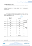
LN2410SBC User’s Manual LN2410SBC Contents 1. 2. 3. 4. 5. INTRODUCTION ........................................................................................................... 2 1.1. Overview...................................................................................................... 2 1.2. LN2410SBC Specification ........................................................................... 2 1.3. Function Block Diagram .............................................................................. 4 Board Configuration...................................................................................................... 5 2.1. Main Power Selection.................................................................................. 5 2.2. Sound Selection ........................................................................................... 6 2.3. SDRAM Chip Select(CS) Selection.............................................................. 7 2.4. Boot ROM Selection .................................................................................... 7 Memory Map ................................................................................................................. 8 3.1. Nor Flash Booting Mode ............................................................................. 8 3.2. NAND Flash Booting Mode ......................................................................... 8 Example Code Tutorials ............................................................................................. 10 4.1. Overview.................................................................................................... 10 4.2. IO_Port....................................................................................................... 10 4.3. UART_Port ................................................................................................ 10 4.4. TIMER........................................................................................................ 11 4.5. WDT (Watch Dog Timer) .......................................................................... 11 4.6. RTC (Real Time Clock) ............................................................................. 12 4.7. ADC (Analog to Digital Converter) ........................................................... 13 Reference.................................................................................................................... 14 5.1. Documentations ......................................................................................... 14 5.2. Books ......................................................................................................... 14 1 www.clabsys.com LN2410SBC 1. INTRODUCTION 1.1. Overview The LN2410SBC is a high performance single board computer based on ARM920T (MMU included). Its ultra low power consumption, various built-in IO ports and support for Linux/WinCE/RTOS make it suitable for many industry applications. ◆ 266MHz clock speed ◆ STN/TFT display support ◆ Compact Flash/MMC/NAND Flash mass storage support ◆ Ethernet and sound support These features provide an ideal development platform for PDA, DVR, image processing and network terminal. 1.2. LN2410SBC Specification ◆ Size : 110×78 mm (2.5 inch) ◆ CPU : S3C2410X (ARM920T) - 266MHz ◆ Memory : - NOR Type Flash : 16Mbit Flash (16bit Bus Interface) - NAND Type Flash : 256Mbit Flash (8bit Bus Interface), NAND Flash Boot - SDRAM : 512Mbit SDRAM (32bit Bus Interface) : 256Mbit×2 ◆ MMC/SD Interface ◆ Compact Flash Interface (Storage type) ◆ 10Mbps LAN : CS8900A ◆ Sound output: Built-in Speaker, Audio Codec. ◆ Infrared sensor (Remote Receiver) ◆ USB Host 1ch ◆ USB Device 1ch ◆ Serial 3ch ◆ JTAG Port 1ch ◆ HDD/CD-Rom Interface www.clabsys.com 2 LN2410SBC ◆ RTC Backup Battery ◆ Status LED 4EA (I/O 2, LAN 2) * STN/TFT LCD support with optional LCD pack * LVDS TFT LCD (10.4 inch) support with optional LVDS pack 3 www.clabsys.com LN2410SBC 1.3. Function Block Diagram S3C2410X ARM 920T JTAG LCD Controller LCD DMA UART0 USB Host Controller UART1 ExtMaster UART2 NAND Controller BUS Controller Arbitor/Decode A H B Interrupt Controller SDRAM (512Mbit) Power Management NOR FLASH (16Mbit) Memory Controller NAND FALSH (256Mbit) B U S Bridge & DMA (4ch) USB Host MMC/SD I/F UART 0,1, 2 IIC USB Device CF I/F USB Device Remote Controller SDI/MMC SPEAKER Watchdog Timer RTC Power BUS Controller Arbitor/Decode Status LED SPI 0, 1 IIS A P B B U S GPIO RTC ADC Timer/PWM 0~3, 4(Internal) Fig. 1-1 www.clabsys.com LAN 4 HDD/CD-ROM I/F Extension Header LN2410SBC 2. Board Configuration Fig. 2-1 2.1. Main Power Selection The main power of LN2410SBC can be provided selectively. Jumper J2 State Description (1-2) USB (2-3) DC supplied from USB host supplied from external power connector J1 or J3 Table 2-1 Main Power selection * Shaded is Default Setting Value If pins (1-2 ) of J2 are connected, power will be supplied from PC USB host port. Due to its limitation to 500mA, an external power supply should be used for optional LCD pack. 5 www.clabsys.com LN2410SBC If pins (2-3) of J2 are connected, power will be supplied from external power supply through J1 or J3 connector. - Through J1 connector: As show in Fig. 2-2, 5 volt should be provided through the hall of which diameter is 2.1mm. A SMPS supplying 5V/1A DC can be used. Fig. 2-2 - Through J3 connector : The J3 was designed to provide power to external devices. However it can be used as an input power terminal to the board as well. Its description is shown in Fig. 2-3 and Table 2-2. Fig. 2-3 Pin Number Description 1 12V 2 GND 3 GND 4 5V Table 2-2 J3 Pin Description 2.2. Sound Selection The sound output is selected by J7. www.clabsys.com 6 LN2410SBC Pin Number (1-2) BUZZER Using TIMER (2-3) IIS SOUND Using CODEC J7 Table 2-3 Sound Selection * Shaded is Default Setting Value When IIS SOUND is selected, mono CODEC signal will be amplified by built-in audio amplifier and drive the built-in speaker. Non amplified audio signal is available through J6 for external speaker or headphone. 2.3. SDRAM Chip Select(CS) Selection By connecting 22 ohm register to R13 or R14, the SDRAM can be located either Bank 6 or Bank 7 respectively. 2.4. Boot ROM Selection The S3C2410X can boot from internal NAND flash memory as well as external boot ROM or flash memory. external flash. The LN2410SBC has 16Mbit NOR type Flash (AM29LV160D) as an And the selection between the two flash memory is made by R9 and R10 when power up. R9 R10 Description ON OFF (0 Ω) (OPEN) ON ON (0 Ω) (0 Ω) OFF ON (OPEN) (0 Ω) * 4-Step Address OFF OFF Boot from NOR Flash(U5 : AM29LV160D) (OPEN) (OPEN) Boot from NOR Flash(U5 : AM29LV160D) NAND Flash : 3-Step Address Boot from NAND Flash(U10 : K9F5608) * 3-Step Address Boot from NAND Flash(U10 : K9F5608) NAND Flash : 4-Step Address Table 2-4 Boot ROM Selection * Shaded is Default Setting Value 7 www.clabsys.com LN2410SBC 3. Memory Map 3.1. Nor Flash Booting Mode The LN2410SBC has 16Mbit NOR type Flash (AM29LV160D) memory which contains bootstrap code for ARMDown. User application can be placed from 0x0001_0000. nGCS7 Reserved nGCS6 SDRAM (U6/U9) nGCS5 Reserved nGCS4 Reserved nGCS3 Reserved nGCS2 CF/HDD nGCS1 LAN (U19) nGCS0 NOR Flash (U5) 0x4000 0000 0x3800 0000 0x3000 0000 0x2800 0000 0x2000 0000 0x1800 0000 0x1000 0000 0x0800 0000 0x0000 0000 Fig. 3-1 Memory Map (NOR Booting Mode) 3.2. NAND Flash Booting Mode In NAND boot mode, the 4KB of the Flash memory is copied to SRAM starting 0x0000_0000 before booting. Therefore, NOR flash memory can be accessed from 0x0000_0400. www.clabsys.com 8 LN2410SBC nGCS7 Reserved nGCS6 SDRAM (U6/U9) nGCS5 Reserved nGCS4 Reserved nGCS3 Reserved nGCS2 CF/HDD nGCS1 LAN (U19) nGCS0 Boot Internal SRAM 0x4000 0000 0x3800 0000 0x3000 0000 0x2800 0000 0x2000 0000 0x1800 0000 0x1000 0000 0x0800 0000 0x0000 0000 Fig. 3-2 Memory Map (NAND Booting Mode) 9 www.clabsys.com LN2410SBC 4. Example Code Tutorials 4.1. Overview Each example folder consists of project file, C or assembly file, library and binary image. They were built under CodeWarrior for ARM Embedded System (Rev 1.2) from Metrowerks. 4.2. IO_Port This example tests I/O ports using Status LED (D2, D3). D2 RA7 VCC3.3 8 7 6 5 1 2 3 4 2 330 2 1 LED0 D3 1 LED1 Fig. 4-1 I/O Port Status LED D2, D3 are connected to GPB5, GPB6 of S3C2410X respectively. After setting GPB5 and GPB6 as output port, write “1” to turn on the LED and “0” to turn off. The code provided was designed to flash the LEDs . The ports initialization is done in boot code and LED_Display() in myLIB.C is called from Main.c . 4.3. UART_Port The S3C2410X UART (Universal Asynchronous Receiver and Transmitter) provides three serial I/O ports (Uart 0/1/2). Among them RxD0, TxD0, nRTS0, nCTS0 for Uart0 are connected to the serial connector. The signals for Uart 1/2 (RxD1, TxD1, RxD2, TxD2) are available through J6 connector. Ex02)Uart shows the UART usage by displaying variables on the serial terminal. The UART related functions are defined in myLIB.c and called from Main.c. Ex03)Calc is a simple calculator which gets the input, 1+2 for example, and displays its result, 3, to serial terminal. The ARMDown built-in serial console or Hyperterminal can be used for serial terminal. www.clabsys.com 10 LN2410SBC 4.4. TIMER The S3C2410X has five 16-bit timers as shown in Fig 6-2. Fig. 4-2 16 bit Timer Block Diagram The timer input clock PCLK, which ¼ of main clock (MCLK: 266MHz) goes through 8bit prescaler and 4bit clock divider before being counted. Ex04)TIMER was designed to flash LED in every second using Timer0. It also displays timer count register (rTCNTO0) on the serial terminal. Other timers can be programmed in similar way. 4.5. WDT (Watch Dog Timer) The S3C2410X watchdog timer is used to generate the reset signal when the system malfunctions. It can be used as a normal 16bit interval timer as well. 11 www.clabsys.com LN2410SBC Fig. 4-3 Watch Dog Timer Block Diagram 4.6. RTC (Real Time Clock) The S3C2410X has a Real Time Clock and Ex06)RTC displays the clock to the serial console. The RTC registers are programmed from Rtc_Set() function in BCD format. An external 32.768 KHz crystal is used for RTC to create 1 second time tick. A backup battery on LN2410SBC supplies power when the system power is off. Figure 6-4 shows power switching between backup battery and external power supply. With external power 1.8 volt is applied to VCCRTC. VCC1.8 R5 1K 2 XTOrtc R6 1K VCC3.3 VCCRTC XTIrtc C11 4 + C9 22pF C8 22pF C10 0.22F,SupurCap DGND Fig. 4-4 www.clabsys.com Q1 2N3906 3 X1 32.768kHz 3 1 12 104 LN2410SBC 4.7. ADC (Analog to Digital Converter) The S3C2410X has 8-channel 10 bit CMOS ADC built in. The analog signals, AIN0/1/2/3/4/5/6/7 are to be provided through extension connector J6. The AIN5/7 are dedicated to touch screen interface, therefore, shouldn’t be used for other purpose. Ex07)ADC reads ADC_DATA of each channel and displays them on the serial terminal. Ex21)Touch shows how to implement touch screen using ADC 13 www.clabsys.com LN2410SBC 5. Reference 5.1. Documentations ArmDown User’s Manual Samsung S3C2410X User’s Manual Samsung S3C2410X Application Note ARM920T Technical Reference Manual ARM Developer Suite User’s Manual 5.2. Books ARM System-On-Chip Architecture (Second Edition) By S.Furber / Addison-Wesley ARM Architecture Reference Manual (Second Edition) By David Seal / Addison-Wesley ARM System Developer’s Guide (First Edition) By Andrew Sloss, Dominic Symes, Chris Wright / Morgan Kaufmann www.clabsys.com 14 LN2410SBC 15 www.clabsys.com