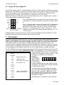
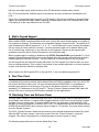
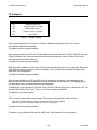
1
TS-3200 User’s Manual TS-3200 User’s Manual Technologic Systems Technologic Systems, Inc. 16525 East Laser Drive Fountain Hills, AZ 85268 480-837-5200 FAX 837-5300 [email protected] http://www.embeddedx86.com/ This revision of the manual is dated May 21, 2009 All modifications from previous versions are listed in the appendix. Copyright © 1998-2001 by Technologic Systems, Inc. All rights reserved. ii 05/21/2009 TS-3200 User’s Manual Technologic Systems Limited Warranty Technologic Systems warrants this product to be free of defects in material and workmanship for a period of one year from date of purchase. Technologic Systems will repair or replace the defective unit during this warranty period in accordance with the following instructions: • Contact Technologic Systems and obtain a Return Material Authorization (RMA) number and a copy of the RMA form. • Fill out the RMA form completely and include it and dated proof of purchase with the defective unit being returned. Clearly print the RMA number on the outside of the package. This limited warranty does not cover damages resulting from lighting or other power surges, misuse, abuse, abnormal conditions of operation, or attempts to alter or modify the function of the product. This warranty is limited to the repair or replacement of the defective unit. In no event shall Technologic Systems be liable or responsible for any loss or damages, including but not limited to any lost profits, incidental or consequential damages, loss of business, or anticipatory profits arising from the use or inability to use this product. Repairs made after the expiration of the warranty period are subject to a flat rate repair charge and the cost of return shipping. Please contact Technologic Systems to arrange for any repair service. iii 05/21/2009 TS-3200 User’s Manual Technologic Systems Table Of Contents LIMITED WARRANTY .............................................................................................................................................. III 1 INTRODUCTION ............................................................................................................................................... 5 2 PC COMPATIBILITY ......................................................................................................................................... 5 2.1 3 4 5 6 7 8 9 10 11 12 13 14 15 Operating Systems ........................................................................................................................................................5 POWER ............................................................................................................................................................. 6 MEMORY........................................................................................................................................................... 6 4.1 4.2 4.3 4.4 SDRAM ..........................................................................................................................................................................6 Flash ..............................................................................................................................................................................6 Flash Expansion ............................................................................................................................................................7 Battery-Backed SRAM ...................................................................................................................................................7 SERIAL PORTS................................................................................................................................................. 8 5.1 5.2 5.3 5.4 Serial Port Configuration Registers................................................................................................................................8 Serial Port Hardware......................................................................................................................................................8 RS-485 Support .............................................................................................................................................................8 Adding Serial Ports ........................................................................................................................................................9 DIGITAL I/O..................................................................................................................................................... 10 6.1 6.2 6.3 DIO1 Header................................................................................................................................................................10 DIO2 Header................................................................................................................................................................10 Using LCD Port as Digital I/O ......................................................................................................................................11 LCD INTERFACE ............................................................................................................................................ 11 MATRIX KEYPAD SUPPORT ......................................................................................................................... 12 REAL TIME CLOCK ........................................................................................................................................ 12 WATCHDOG TIMER AND SOFTWARE RESET ........................................................................................... 12 LED.................................................................................................................................................................. 14 JUMPERS........................................................................................................................................................ 15 PC/104 BUS EXPANSION .............................................................................................................................. 16 LOADING OR TRANSFERRING FILES.......................................................................................................... 17 14.1 Developing with Technologic Systems TS-9500..........................................................................................................17 14.2 Zmodem Downloads ....................................................................................................................................................17 14.3 Manufacturing Mode ....................................................................................................................................................17 DEBUGGING................................................................................................................................................... 18 15.1 Integrated BIOS Debugger ..........................................................................................................................................18 15.2 Using other debuggers.................................................................................................................................................19 16 VIDEO, KEYBOARD, AND CONSOLE REDIRECTION ................................................................................. 19 17 FEEDBACK AND UPDATES TO THE MANUAL ............................................................................................ 19 APPENDIX A - BOARD DIAGRAM AND DIMENSIONS.......................................................................................... 20 APPENDIX B – SYSTEM MEMORY MAP ............................................................................................................... 21 APPENDIX C – SYSTEM I/O MAP .......................................................................................................................... 22 APPENDIX D - BIOS INTERRUPT FUNCTIONS .................................................................................................... 23 Int 15h / Function B000h - Technologic Systems BIOS information......................................................................................23 Int 15h / Function B010h - LED Control ................................................................................................................................23 Int 15h / Function B040h – Matrix Keypad Support...............................................................................................................24 Int 15h / Function B042h – Alpha-Numeric LCD Support......................................................................................................24 Int 15h / Function B021h – JP5 Status..................................................................................................................................24 Int 15h / Function B020h - Jumper Pin Status.......................................................................................................................25 APPENDIX E - DIRECT CONTROL OF THE 386EX DIO PINS ............................................................................. 26 APPENDIX F - USING A 12.5 MHZ BAUD CLOCK................................................................................................. 27 APPENDIX G - FURTHER REFERENCES ............................................................................................................. 27 APPENDIX H - MANUAL REVISIONS..................................................................................................................... 28 iv 05/21/2009 TS-3200 User’s Manual Technologic Systems 1 Introduction The model TS-3200 is a compact, full-featured PC compatible Single Board Computer based on the 386EX processor. If you are coming up from the 8-bit microcontroller world, you will find that this product provides much more performance and much quicker development since you can now use standard PC development tools such as Turbo C or Quick Basic. If you have done work in the PC world in the past, you will find you can now build applications for a very small target that does not require a keyboard, video, floppy disks, or hard drives. You can typically write and debug code on a host PC using standard development tools for the PC platform, then simply copy it to and run it on the TS-3200 without modification. If additional peripherals are required, the PC/104 expansion bus allows for many standard functions available off-the-shelf. It is also very simple to create a custom PC/104 daughter board for those special features that differentiate your product. Technologic Systems can provide technical support as well as a free quotation for any custom hardware, software, or BIOS modifications you may require. This manual is fairly short. This is because for the most part, the TS-3200 is a standard 80386-based PC compatible computer, and there are hundreds of books about writing software for the PC platform. The purpose of this manual is documenting where the TS-3200 differs from a standard PC. 2 PC Compatibility PC compatibility requires much more than just a 386 processor. It requires PC compatible memory and I/O maps as well as a PC compatible BIOS. The General Software EMBEDDED BIOS offers a high degree of compatibility with past and present BIOS standards allowing it to run off-the shelf operating systems and application software. The EMBEDDED BIOS has been tested with all major versions of DOS, including MS-DOS, DR-DOS, and Embedded DOS 6-XL; all major versions of OS/2, including MS-OS/2 and IBM OS/2; MS-Windows 3.1, Windows-95, Windows NT, and NetWare 386. 2.1 Operating Systems Technologic Systems Embedded PCs are compatible with a wide variety of x86-based operating systems. A partial list OSes currently used with our boards by customers includes: • TNT Embedded Toolsuite, Phar Lap Software • UCos II • RTKernel, On Time Software • RTEMS, On-Line Applications Research Corporation • DOS with WATTCP, public domain TCP/IP source code for DOS • Linux The TS-3200 is shipped, free of charge, with Embedded DOS ROM by General Software. The TS-3200 can be shipped upon request with Linux pre-installed for a nominal fee. The Linux file system and kernel is also freely available on the web should you wish to install it yourself. The Linux OS requires a 16MB or larger Compact Flash or an M-System’s DiskOnChip. 5 05/21/2009 TS-3200 User’s Manual Technologic Systems 3 Power The TS-3200 requires regulated 5VDC at 375mA (typical). A quick release screw-down terminal block for the 5V power and power GND connections is provided for easy connection to an external power supply. When power is first supplied to the TS-3200, the board mounted LED is immediately turned on under hardware control. Once the processor begins execution, the LED is turned off. The LED then turns on then off to provide a characteristic blink during execution of POST. If the LED does not turn on at all, the most likely problem is the power supply. Check that the +5V and GND connections are not reversed. A diode protects the board against damage in such a situation, but it will not run. Please note that supply voltages over 6VDC may damage the TS-3200. Be sure to use a regulated 5VDC power supply. 4 Memory 4.1 SDRAM The TS-3200 has a total of 8 Megabytes of high-speed SDRAM providing 640 KB of base memory, 7 Megabyte of extended memory, and 128 KB of shadow RAM for the BIOS and DOS-ROM. This is identical to a standard PC memory map. The TS-3200 can be ordered with 16MB or 32MB of SDRAM, but it is not field upgradeable. If using DOS, then the 7 Megabyte of extended memory can be used as a RAM disk by adding the vdisk.sys device driver. The RAM disk is accessible as drive C: if the DiskOnChip 2000 Flash disk is not installed, drive D: if it is. The size of the disk can be reduced to provide extended memory for an application (or simply removed entirely) by editing the CONFIG.SYS file in the root directory of drive A:. Please see the BIOS/DOS User's Manual for further information on vdisk.sys. 4.2 Flash There is a total of 1 MB of Flash memory on the TS-3200. The top 128 KB of Flash are reserved for the BIOS and DOS-ROM. During POST, they are copied from Flash into DRAM at addresses E0000h through FFFFFh for improved performance (a standard technique known as BIOS Shadowing). The remainder of the Flash memory (896 KB) is used by a SSD (solid state disk) appearing as drive A. The SSD is fully supported by the BIOS as an INT 13h drive. The flash memory can be populated using a 2 MB chip instead of a 1 MB. This option provides additional storage space and is less expensive than adding an 8 MB DiskOnChip module. The physical Flash memory is accessed by the BIOS in protected mode at memory address 52M. The Flash memory is guaranteed capable of a minimum of 100,000 write/erase cycles. This means that if you completely erase and rewrite the SSD drive 10 times a day you have over 27 years before any problems would occur. Reading the SSD produces no wear at all. The flash drive is read-only when JP3 is not installed. See Section 12 for more information. 6 05/21/2009 TS-3200 User’s Manual Technologic Systems 4.3 Flash Expansion If 896 KB of Flash is insufficient for your application, an empty 32-pin socket is available for Flash expansion using an M-Systems DiskOnChip 2000 or DiskOnChip Millennium Flash Drive. This product is a wonder of miniaturization; it is a complete Flash SSD in a single 32 pin package currently available in sizes from 8 MB up to 288 MB. The DiskOnChip is available from Technologic Systems as well as other distributors. It is compatible with DOS as shipped, and drivers for other operating systems are available. A DiskOnChip of 16 MB or larger is required for the TS-3200 to run under Linux. For the TS-3200, Technologic Systems offers a complete Linux Operating System configured for a small footprint that runs under the Linux kernel. When using the DiskOnChip, it will simply appear as drive C: The DiskOnChip uses the 8 KB range of D0000h through D1FFF in memory space. If you are installing a PC/104 daughter card that uses memory mapped I/O, it must not conflict with this address range if the DiskOnChip is installed. If it is not installed, there will be no conflict 4.4 Battery-Backed SRAM The 32-pin socket can also optionally hold 32 KB of battery-backed CMOS SRAM memory. This or the DiskOnChip may be installed, but not both. Unlike Flash memory, battery backed SRAM provides non-volatile memory with unlimited write cycles and no write time degradation. The SRAM uses the 32 KB memory range of D0000h through D7FFFh. If the SRAM is installed, PC/104 daughter cards that uses memory mapped I/O must not conflict with this address range. 7 05/21/2009 TS-3200 User’s Manual Technologic Systems 5 Serial Ports The two PC compatible asynchronous serial ports provide a means to communicate with external serial devices such as printers, modems, etc. Each is independently configured as a standard PC COM port which is compatible with the National Semiconductor’s NS16C450. COM1 appears in the I/O space at 3F8h and uses IRQ4. COM2 is located at 2F8h and uses IRQ3. The COM ports use a master clock of 1.8519 MHz as compared to a standard clock of 1.8432 MHz. This results in an error for all baud rates of .0047 (less than ½%). The error is insignificant and this clock value allows standard baud rate selections -- for example a divisor of 12 yields 9600 baud. By changing an internal configuration register in the 386EX, the serial clock can be switched to 12.5 MHz (the processor clock divided by 2). This feature allows baud rates higher than 115 kbaud (up to 781 kbaud), as well as low error, non-standard lower baud rates (such as 24 kbaud). See Appendix F for further information. The COM ports may also be configured to use a DMA channel, which is handy when very high baud rates are being used. When enabled, a DMA request is issued any time a serial port’s receive buffer is full or its transmit buffer is empty. This allows higher speed operation with much lower CPU overhead. See the Intel 386EX User's Manual for further details. 5.1 Serial Port Configuration Registers Because both serial ports are 100% PC compatible, software written for the PC that accesses serial ports directly or through standard BIOS calls will work without modification on the TS-3200. The details of the COM port internal registers are available in most PC documentation books or the data sheet for the National Semiconductor NS16C450 may be consulted. 5.2 Serial Port Hardware Each serial port has 4 lines buffered: the two data lines and the CTS / RTS handshake pair. This is quite sufficient to interface with the vast majority of serial devices. The serial lines are routed to 10 pin headers labeled COM1 and COM2. A serial adapter cable can be plugged into the header to convert this into a standard DB9 male connector. The pin out for the 10 pin header and DB9 male connector are listed below. The RTS signal also drives the DTR pin on the serial ports; DTR is always the same state as RTS. In addition, RTS is also used to enable the RS-485 transmitter (see below for more details). 5V Power NC [in] CTS [out] RTS RS-485 TX- / RX- * 10 9 8 7 6 5 4 3 2 1 GND DTR (RTS) [out] TX data [out] RX data [in] RS-485 TX+ / RX+ * Figure 1 - Serial Port Header and DB9 Pinout [signal direction is in brackets] * RS-485 is optional PLEASE NOTE: The serial port headers use a non-standard numbering scheme. This was done so the header pins would have the same numbering as the corresponding DB-9 pin; i.e. pin 8 (CTS) on the header connects to pin 8 on the DB-9 5.3 RS-485 Support An option is available to add support to COM1 for half-duplex RS-485. RS-485 drivers allow communications between multiple nodes up to 4000 feet (1200 meters) via twisted pair cable. Half-duplex RS-485 requires one twisted pair plus a Ground connection. Full-duplex RS-485 is not supported on the TS-3200. Full Duplex is supported by the TS-3300 and TS-5300 products. For half-duplex operation, a single twisted pair is used for transmitting and receiving. The serial port's RTS signal controls the RS-485 transmitter/receiver. When RTS is asserted true (bit 1 of the modem control register = 1), the RS-485 transmitter is enabled and the receiver disabled. When RTS is deasserted the transmitter is tri-stated (disabled) and the receiver is enabled. Since the transmitter and receiver are never both enabled, the serial port UART does not receive the data transmitted. The 8 05/21/2009 TS-3200 User’s Manual Technologic Systems transmitter and receiver share a single pair of signals that are available on pins 1 and 6 of the COM1 10-pin header, as well as on the 3-pin terminal block connector. When COM1 is configured for RS-485 usage, the COM1 RS-232 port must not be connected. Data received on the RS-232 port will corrupt RS-485 data. RS-485 Quick start procedure: It is possible to use COM1 in RS-232 mode even when the 1. The RS-485 option must be installed RS-485 option has been ordered. To disable RS-485 (and enable RS-232) on COM1, simply remove the 8-pin RS-485 2. Attach the RS-485 cable to pins 1 and 6 of the COM1 header or the 3-pin transceiver from the 8-pin socket (near the center of the RS-485 header. board). 5.4 Adding Serial Ports If your project requires more than two serial ports, additional ports may be added via the PC/104 expansion bus. Technologic Systems currently offers a 2 serial / 1 parallel port card, the TS-SER2, and other manufacturers sell cards with up to four additional serial ports. Typically these would be configured as COM3 or COM4 or be assigned other nonstandard I/O locations. Because DOS only directly supports four serial ports, any additional ports beyond four will require software drivers. 3. Set the COM1 UART serial parameters (baud rate, data, parity, and stop bits, interrupts, etc). 4. To transmit data, assert RTS and write the data to the UART 5. To receive data, deassert RTS and read the data from the UART The PC/104 bus has IRQ3, 4, 5, 6, 7 or 9 available for additional serial ports. If IRQ3 or 4 are to be used on a PC/104 expansion card, then care must be taken since COM2 and COM1 also use these IRQs, respectively. For example, if IRQ4 is used for COM3 then either COM1 must be used in a noninterrupt fashion or only one COM port can have the interrupt enabled at a time. In any case only one COM should have the Interrupt Enable (Bit 3 of Modem Control Reg.) set at any one time if they share the same IRQ. This is a standard problem with the PC architecture. A better solution is to simply use interrupts other than 3 or 4 for additional serial ports. 9 05/21/2009 TS-3200 User’s Manual Technologic Systems 6 Digital I/O There are 37 Digital Input/Output (DIO) lines available on the TS-3200. These are available on 3 headers labeled DIO1, DIO2, and LCD. In addition to the DIO signals, each header also has 5 Volt power and Ground available. The header labeled LCD can be used as 11 DIO lines or as an alphanumeric LCD interface (See Section 7). 16 of the DIO lines are arranged as two byte-wide ports that can be programmed as either inputs or outputs in groups of 4-bits. Most of the remaining 21 DIO lines are fixed as either input or output signals. 6.1 DIO1 Header The DIO1 port provides +5V, GND, and 12 digital I/O lines that can be used to interface the TS-3200 to a wide range of devices. Some of these signals have dual functions, some are input or output only, while some are programmable (can be either inputs or outputs). For example, DIO1 pins 6, 11, 12, and 13 are by default IRQ7, IRQ3, IRQ4, and IRQ5 respectively. These lines can be changed to general-purpose inputs by changing a configuration register in the 386EX (see Appendix E ). In all cases, these signals can only be inputs. 14 13 IRQ5 / P3.3 12 11 IRQ3 / P3.1 10 9 RI2 / SRXD 8 7 RTS2 / STXD 6 5 P1.0 4 3 P3.6 2 1 5V Figure 2 – DIO1 Header Pinout IRQ1/ P3.2 IRQ4 / P3.0 DTR2 / SRXCLK DSR2 / STXCLK IRQ7 / P3.5 P1.5 GND DIO1 pins 7 through 10 are COM2 handshake lines that can be used as digital I/O with pins 8 and 9 inputs only and pins 7 and 10 as outputs only. Alternatively, pins 7 through 10 can be used as a synchronous serial port by changing 386EX configuration registers. Pin 14 is shared with Jumper 5 (JP5). Pin 14 is used as IRQ 1 when the TS-9500 daughter board is installed. If JP5 is not being used and the TS-9500 is not installed, it can be used for digital I/O. Pins 3, 4, 5, and 14 can be programmed as either inputs or outputs. All digital outputs can source or sink up to 8mA. All digital inputs have standard TTL level thresholds. If configured as inputs, they should not be driven below 0 Volts or above 3.3 Volts! All other inputs should not be driven below 0 Volts or above 5.0 Volts. For further information on configuration and use of these pins, please see Appendix E . 6.2 DIO2 Header 5 V 16 15 DIO 2_7 P1.3 14 13 DIO 2_6 The odd numbered pins 1-15 provide 8 bits of byte-wide digital I/O IRQ6 / P3.4 12 11 DIO 2_5 addressed at I/O location 7Eh. The upper 4 bits or lower 4 bits can be DCD2 10 9 DIO 2_4 independently selected as input or output. RTS1 8 7 DIO 2_3 P1.2 6 5 DIO 2_2 Bits 0 and 1 at I/O location 7Dh controls the direction, when bit 0 = ”0” LED_ON 4 3 DIO 2_1 the lower 4 bits (pins 1, 3, 5, and 7) are inputs. If bit 0 = “1”, then they GND 2 1 DIO 2_0 are outputs. These pins have 4.7k ohm resister pull-ups to 5V. Figure 3 – DIO2 Header Pinout The DIO2 Port provides +5V, GND, and 14 digital I/O lines. Bit 1 at I/O location 7Dh controls the upper 4 bits (pins 9, 11, 13, and 15) in a like manner. At reset bits 0 and 1 at I/O location 7Dh are set to zero, which initializes all of these pins as inputs. Pins 4 and 8 are always outputs and pin 12 is always an input. Pins 6 and 14 are programmed as inputs or outputs (see Appendix E ). If pins 6 or 14 are used as inputs they should not be driven below 0 Volts or above 3.3 Volts! All other inputs should not be driven below 0 volts or above 5.0 Volts. 10 05/21/2009 TS-3200 User’s Manual Technologic Systems 6.3 Using LCD Port as Digital I/O The LCD Port can be used as 11 additional digital I/O lines or it can be used to interface to a standard alphanumeric LCD display. At system reset, the port defaults to DIO mode. If using an LCD display this port can be switched to LCD mode by writing a 1 into bit 4 at I/O location 7Dh, or the BIOS c all to enable the LCD also sets bit 4 at I/O location 7Dh (See Section 7 for LCD mode). When the LCD port is in DIO mode, pins 3 and 6 are digital inputs, pin 5 is a digital output, and pins 7 – 14 are programmable as either inputs or outputs. 14 13 LCD_7 12 11 LCD_5 10 9 LCD_3 8 7 LCD_1 6 5 EN 4 3 RS 2 1 5V Figure 4 – Pinout for LCD header when used as DIO LCD_6 LCD_4 LCD_2 LCD_0 WR Bias GND Pins 3 (RS) and 6 (WR) can be read at I/O location 73h bits 7 and 6, respectively. Pin 5 (EN) is controlled by writing to I/O location 73h bit 0. Pins 7 –14 can be read or written at I/O location 72h. The direction of the byte-wide port (pins 7 – 14) at I/O location 72h is controlled by bits 2 and 3 at I/O location 7Dh. If bit 2 is a zero, then the lower 4 bits (pins 7 – 10) are inputs. If bit 2 is logic 1, then pins 7 – 10 are outputs. Bit 3 at location 7Dh controls the upper 4 bits, pins 11 – 14 in a like manner. All digital outputs on this port can source or sink 4 mA and the digital inputs have standard TTL level thresholds and must not be driven below 0 Volts or above 5.0 Volts. 7 LCD Interface A 14-pin LCD connector is provided on the TS-3200 for interfacing with standard alphanumeric LCD displays. These displays use a common controller, the Hitachi HD44780 or equivalent. While software written for the HD44780 will work with all displays using the controller, the cable needed is dependent on the display used. For most displays, a straight-through type ribbon cable can be used. The connector on the LCD display is typically mounted on the backside of the display. Warning – using an incorrect cable or mounting the LCD connector on the front-side can result in a reverse power polarity and can damage the LCD display. Please refer to your LCD data sheets for in-depth information. The TS-3200 BIOS incorporates a fairly complete set of INT10h video routines that work with the LCD. Once the LCD has been enabled (INT15h/Func B042h – see Appendix D ) , the LCD can be written to using the standard BIOS routines. This includes the Pin Function Comments majority of PC languages, such as C and C++. See 1 LCD 5V the programs included on the utility disk for 2 LCD GND examples. 3 RS Register Select (A0) 4 Bias 680 Ohm to GND 5 EN LCD Enable (Active High) 6 WR# 7 LCD_1 8 LCD_0 9 LCD_3 10 LCD_2 11 LCD_5 12 LCD_4 13 LCD_7 14 LCD_6 Write (Active Low) LCD0 – LCD7: Buffered bi-directional data bus 2 4 6 8 10 12 14 I/O addresses 1 3 5 7 9 11 13 72h and 73h are Figure 5 - LCD Header Pinout used to access the LCD. Figure 5 shows the header pin-out, while Table 2 lists the LCD signals. The section below will briefly describe the LCD interface signals. The RS signal is simply the buffered A0 address line. Thus, reads and writes to 72h cause register select to be low, and those to 73h cause it to be high. Generally the LCD uses this line to separate data bytes from command bytes. See your LCD data sheet for details. The WR# signal is an active low write enable line. Table 1 - LCD Header Signals 11 05/21/2009 TS-3200 User’s Manual Technologic Systems EN is an active high signal, raised whenever the LCD addresses are being read or written. D0 – D7 are bi-directional, buffered copies of the data bus and carry all data and commands to the LCD. Figure 5 is not the standard pin-outs given for LCD displays. But this pin-out allows a standard ribbon cable to be used when the ribbon cable is attached to the backside of the LCD. Example code for the LCD display is on the utility diskette for the TS-3200. 8 Matrix Keypad Support The DIO2 port, signals DIO2_0 through DIO2_7, may be configured to support a 4 x 4 matrix keypad. When enabled, BIOS firmware performs all the work, making the matrix keypad appear as a simple 16key keyboard to software. This allows the use of standard keyboard access routines. The default set of keys translated by the BIOS consists of 0 – 9, A – D, *, and #. Because the user is writing the software, this set of keys is usually sufficient. However, a custom translation table can be loaded, allowing the use of function keys, arrow keys, or any other key on the keyboard. Please see the sample code included on the utility disk for further information on the translation table. Matrix keypad support is enabled or disabled using INT15h, Function B040h (see Appendix D ). Once enabled, standard keyboard BIOS functions are enabled. Note that console redirection and the matrix keypad support are mutually exclusive – console redirection must be disabled to use the keypad. A matrix keypad can be used with console redirection only if the keypad is not used as stdin, but read from as a hardware device. This is useful if one wishes to use console redirection or to use a keyboard as stdin. See the utility diskette for example code. When enabled, the DIO2 signals DIO2_0 through DIO2_7 are not available as general I/O. 9 Real Time Clock The Dallas Semiconductor DS12887 is used for the PC compatible battery-backed real-time clock. It is a completely self-contained module that includes a Motorola 146818 compatible clock chip, the 32.768 kHz crystal, the lithium battery, and 114 bytes of battery-backed CMOS RAM. It is guaranteed to maintain clock operation for a minimum of 10 years in the absence of power. It is located at the standard PC I/O addresses of Hex 070 and 071. The top 32 bytes of battery-backed RAM (index 60h through 7Fh) are not used by the BIOS and are available for user applications. 10 Watchdog Timer and Software Reset The Intel 386EX contains a 32-bit watchdog timer (WDT) unit that can be used as a watchdog timer or as a software reset function. A system reset is asserted when the WDT times out preventing a system “hanging” due to a software bug. To prevent a WDT timeout, the application must periodically “feed” the WDT by writing to a specific I/O location (WDTCLR). The value loaded into the 32-bit down-counter (WDTRLDH and WDTRLDL) allows timeout values as high as 170 seconds. This value will be referred to as the “Reload Constant”. The 32-bit “Reload Constant” determines the maximum time allowed between each Watch Dog Feed. After the WDT has been started, it cannot be turned off and the “Reload Constant “ cannot be changed. This makes it impossible for a crashed program to cause a system to “hang”. The following steps outline how to start the Watch Dog Timer: 12 05/21/2009 TS-3200 User’s Manual Technologic Systems 1) Write to the upper 16 bits (WDTRLDH at 0F4C0h) of the reload value (the number of clock cycles before the watchdog timer times out) followed by a write to the lower 16 bits (WDTRLDL at 0F4C2h) of the reload value. 2) Perform a Watch Dog Feed. Write 2 sequential words: 0F01Eh followed by 0FE1h to the watchdog timer clear register (WDTCLR). The WDTCLR is located at 0F4C8h. 3) Software must periodically perform step two (the Watch Dog Feed) before the watchdog timer times out to prevent a system reset. Each increment in the value of the upper 16-bits (WDTRDH) of 32-bit Reload Register adds 2.62 mS to the Watch Dog Timeout Value. The lower 16 bits (WDTRDL) are insignificant and can be loaded with zero. This fact allows the following simple method of calculating a “Reload Constant” (assuming a 25MHz 386EX clock): For example: if a 2 second time-out is desired, then So WDTRLDH = 02FBh and WDTRLDL = 0000 When the WDT times out, it causes a complete hardware reset to the entire TS-3200 and also asserts RESETDRV on the PC/104 Bus. The following code illustrates using the WDT to implement a software reset routine. The WDT is initialized with a very low “Reload Constant”. Void main () { const int WDTCLR = 0xF4C8; const int WDTRLDH = 0xF4C0; const int WDTRLDL = 0xF4C2; int n = 0; outport(WDTRLDH, 0x0001); // Reload Constant = 2.6 mS outport(WDTRLDL, 0x0000); // outport(WDTCLR, 0xF01E); // Watch Dog Feed word 1 outport(WDTCLR, 0x0FE1); // Watch Dog Feed word 2 for (n =0; n = 1; ) { //endless loop…system will //be reset in about 2.62 milliseconds anyway 13 05/21/2009 TS-3200 User’s Manual Technologic Systems } return –1; } For more information, please see Intel’s 386EX manual, chapter 17, for more information. 11 LED The TS-3200 has a green LED available for user software. Example uses include diagnostics, status messages, and simple output. This signal is also available as a digital output on the DIO2 header. When power is first supplied to the TS-3200, the board mounted LED is immediately turned on under hardware control. Once the processor begins execution, the LED is turned off, then flashed on and off again briefly. If the LED does not turn on at all, the most likely problem is the power supply. Check that the +5V and GND connections are not reversed. A diode protects the board against damage in such a situation, but it will not run. BIOS interrupt functions are used to turn the LED on and off. Please see Appendix D for further details and the utility disk for example code. 14 05/21/2009 TS-3200 User’s Manual Technologic Systems 12 Jumpers Jumper Function JP1 JP2 JP3 JP4 JP5 Manufacturing Mode Console Enable on COM2 Write Enable Drive A: Reduce Clock to 12.5 MHz User Jumper Table 2 - Jumper Listing With a jumper installed on JP1, the unit switches to Manufacturing Mode. See 14.3 for more information on Manufacturing Mode. The default is with no jumper installed. With a jumper installed on JP2, the TS-3200 redirects all console activity to COM2. With JP2 removed, COM2 is available as a Com port and all console activity behaves as normal. Section 16 for more information about console redirection. The default is with the jumper installed. With the jumper installed on JP3 on the TS-3200, the on-board flash (drive A:) is read-write. Removing JP3 results in read-only access to the on-board flash. This is most useful to disable changes to the flash drive in the end product. The default is with the jumper installed. With a jumper installed on JP4, the 386EX clock is throttled to half speed. One advantage of this feature is that this will reduce the amount of power consumed. Another benefit is for debugging; this can help resolve timing related issues during development. The Baud Rate Clock and the PC/104 Bus clocks (SYSCLOCK and OSC) are not affected by JP4. The internal 386EX Watch Dog Timer, Timer 1, and Timer 2 clocks are affected. The default is no jumper installed. JP5 is a jumper reserved for user programs. This jumper is shared with 2 other functions. Note: If the TS-9500 daughter board is used, then JP5 must not be installed. Note: JP5 can also not be used if DIO1 Port Pin 14 is being used. The default is with no jumper installed. The status of any jumper can be read via a BIOS call. See Appendix D for more details. 15 05/21/2009 TS-3200 User’s Manual Technologic Systems 13 PC/104 Bus Expansion The PC/104 is a compact implementation of the PC/AT ISA bus ideal for embedded applications. Designers benefit from using an already-developed standard, Pin # Signal Name rather than creating their own. Further, the presence of a compact B5 -5V form-factor PC compatible standard has encouraged the B6 DRQ2 development of a broad array of off-the-shelf products, allowing a B7 -12V very quick time to market for new products. B8 ENDXFR# B9 +12V B15 DACK3# ‡ B16 DRQ3 ‡ B17 DACK1# B18 DRQ1 B26 DACK2# B27 TC Table 3 - Unsupported PC/104 Signals on the 8-bit Bus ‡ PC/104 expansion cards must not connect to these pins. Pin # C1 C2 – C8 Signal Name SBHE# LA23 – LA17 C9 MEMR# C10 MEMW# C11-18 D8 – D15 D1 MEM16# D2 IO16# D7 IRQ14 Table 5 – Supported signals on the optional 16-bit PC/104 The electrical specification for the PC/104 expansion bus is identical to the PC ISA bus. The mechanical specification allows for the very compact implementation of the ISA bus tailor made for embedded systems. The full PC/104 specification is available from the IEEE Standards Office under # IEEE P996.1 (see Appendix G for further information). Basically, this bus allows multiple daughter boards in a 3.6 inch by 3.8-inch form factor to be added in a selfstacking bus. Since the electrical specs are identical (except for drive levels) to a standard PC ISA bus, standard peripherals such as COM ports, Ethernet, video, LCD drivers, and Flash drives may be easily added using standard drivers. The TS-3200 implements an 8-bit or 16-bit version of the PC/104 bus with a few signals not supported. We have found this allows the support of the vast majority of PC/104 boards including all of the above mentioned examples. The one feature missing is DMA, which few PC/104 boards use. Pin # Signal Name A1 IRQ1† A2 - A9 D7 – D0 A10 IOCHRDY A11 EN A12 - A31 A19 – A0 A32 GND B1 GND B2 RESETDRV B3 +5V B4 IRQ9 B11 SMEMW# B12 SMEMR# B13 IOW# B14 IOR# B19 User Chip Select # B20 SYSCLK (8.33 MHz) B21 IRQ7 † B22 IRQ6 † B23 IRQ5 † B24 IRQ4 † B25 IRQ3 † B28 BALE B29 +5V B30 OSC B31 GND B32 GND Table 4 - Supported PC/104 Signals On the 8-bit Bus † These signals are also connected to the DIO ports. Pin B19 (normally not used) has been reassigned to be a User Chip Select. This active low signal decodes the I/O address range 140h through 15Fh, to allow for simple low-cost daughter board designs. The User Chip Select uses the 386EX CS0. This can be easily programmed to be at any I/O location or memory range. This pin can also be used for general purpose I/O as bit 0 of Port 2 of the 386EX. All Technologic Systems 3000 and 5000 series products will support this feature. 16 05/21/2009 TS-3200 User’s Manual Technologic Systems 14 Loading or Transferring Files Three methods are available for transferring files between a desktop PC and your TS-3200: Compact Flash (with TS-9500), Zmodem downloads, and Manufacturing Mode. Full descriptions of each are detailed below. Other programs which use serial ports to transfer should work as well (for example, FastLynx). 14.1 Developing with Technologic Systems TS-9500 The TS-9500 daughter board features a removable Compact Flash Card that behaves like a standard IDE drive. This allows two different development methods. 1. Develop on a host system. Transfer files to the TS-3200 via the compact flash card on the TS9500. Technologic Systems offers a low-cost SanDisk USB compact flash card interface for your host system. 2. Transfer your development tools (e.g. Turbo C) onto the compact flash card. Now you can compile, debug, and execute right on the TS-3200 target. The TS-9500 also provides full VGA video, keyboard, and mouse interfaces necessary to work within most environments. 14.2 Zmodem Downloads Using the Zmodem protocol to send files to and from the TS-3200 is simple and straightforward. The only requirement is a terminal emulation program that supports Zmodem, and virtually all do. If you are using Windows 95 or later for your development work, the HyperTerminal accessory works well. To download a file to the TS-3200 from your host PC, execute DL.BAT at the DOS command line on the TS-3200 (while using console-redirection from within your terminal emulator) and begin the transfer with your terminal emulator. In HyperTerminal, this is 'Send File...' from the 'Transfer' menu. To upload a file from the TS-3200 to your host PC, execute UL.BAT <FILENAME> at the DOS command line on the TS-3200 and start the transfer in your terminal emulator. Many emulators, HyperTerminal among them, will automatically begin the transfer themselves. Occasionally there may be errors in transmission due to background solid state disk operations. This is not a problem -- Zmodem uses very accurate CRC checks to detect errors and simply resends bad data. Once the file transfer is complete the file is completely error free. Please note that the utility used to perform Zmodem file transfers on the TS-3200 side is called DSZ, produced by Omen Technologies. DSZ is shareware -- it is not free. If you decide to use it, you are legally obligated to pay Omen Technologies. Currently the cost is $20. Further info is available in the DSZ zip file located on the utility disk, and contact info for Omen Technologies is in Appendix G. 14.3 Manufacturing Mode The TS-3200 has a special feature called 'Manufacturing Mode' which makes the on-board Flash SSD appear as just another drive on your desktop computer using a DOS device driver and a serial cable. First, connect a null modem cable between COM2 on the TS-3200 and COM1 or COM2 of your desktop computer. Next, the TS-3200 must be placed in Manufacturing Mode. To do so, install jumper JP1 and power cycle the unit. Manufacturing Mode will automatically start once the POST routines have been executed. At this point, the TS-3200 will simply sit and wait for serial packets to arrive from a host. Now install the Manufacturing Mode driver on your desktop computer. To do so, simply copy the MFGDRV.SYS device driver from the utility disk to anywhere on your desktop machine's hard drive. Then insert the following line in your CONFIG.SYS file and reboot: DEVICE=<PATH>\MFGDRV.SYS /UNIT=0 /BAUD=38K /PORT=COMX 17 05/21/2009 TS-3200 User’s Manual Technologic Systems Where <PATH> is the full path to the location where you copied the MFGDRV.SYS driver, and X is the port on your host PC that the null modem cable is connected to (1 or 2). The Flash SSD drive should now appear on the next free drive letter on your desktop computer (usually the D: or E: drive). Simply copy your program onto the drive, and that's it! You can create directories, edit files, and even execute programs on your desktop computer over the Manufacturing Mode link just the way you would with a regular disk drive, just a bit more slowly. When you are finished, turn off the TS-3200, remove the jumper, and turn it back on. Your program (if loaded into the autoexec) will now execute every time the TS-3200 is turned on. While Manufacturing Mode is in operation, the board LED provides feedback. While idle, the LED will cycle on and off at approximately 1/2 Hertz. While data is being transferred, it will cycle much more rapidly (anywhere from 5 to 1000 Hertz) NOTE: The Manufacturing Mode driver currently does not work correctly with Windows 95 or later. Please use the Zmodem method if you are using Windows environment. You may need to boot directly to DOS using the utility diskette supplied with your unit if you wish to use the Manufacturing Mode method. The utility diskette will boot to DOS ROM 4.04 with the maufacturing mode driver installed. The flash drive can now be accessed and restored using the floppy. 15 Debugging There are two main methods for debugging on the TS-3200: using the integrated BIOS debugger (INT3) and/or using your development tool's debugger (this usually requires the TS9500 video and keyboard). 15.1 Integrated BIOS Debugger To provide simple, direct access to the TS-3200 hardware, the system BIOS has an integrated debugger that can perform standard low-level debugger functions. The debugger allows you to perform operations such as disassemble code, display and alter the contents of memory, write to and read from I/O ports, and single-step through or breakpoint code. The debugger is not intended for use as the only debugging tool for applications, but it can be a real lifesaver when you need interactive, direct access to hardware. The BIOS debugger can be entered by any of several methods: • The debugger hooks the CPU exception vectors in case a divide by zero occurs, an invalid opcode is executed, or an INT 3 instruction is executed, for example. By placing an INT 3 instruction in your application code the debugger will automatically be invoked. To resume, type the 'G' command to "GO", or continue on with the rest of initialization. • From DOS-ROM by typing ‘INT3’ at the command prompt. If the full command.com interpreter is running, this is an internal command. If only mini-command.com is running, this will execute a small utility that simply contains an ‘INT 3’ instruction. • From the BIOS Setup main menu (started by typing ‘ctrl-C’ during the BIOS POST), the ENTER SYSTEM BIOS DEBUGGER selection will enter the debugger. After use, typing the ‘G’ (go) command will return to the SETUP screens. • As a boot action, as a last-ditch effort if the operating system cannot be booted from the appropriate drives or out of ROM. A complete discussion of debugger commands is available in the Integrated BIOS Debugger Reference Manual, included on the TS-3200 Utility Disk and also available from the Technologic Systems web site. Entering ‘?’ will list all available commands, and a ‘g’ (go) will return execution to the point where the debugger was called. 18 05/21/2009 TS-3200 User’s Manual Technologic Systems 15.2 Using other debuggers For example, the Turbo C debugger can be used on the target board using the TS-9500 video and keyboard interfaces. Any other standard PC software debugger of your choice should work just as well. 16 Video, Keyboard, and Console Redirection The TS-3200 has no video controller or keyboard interface. This was done to keep the board size small and the cost low. For applications that require it, a PC/104 video board can be added to the system easily. Technologic Systems recommends the TS-9500, a PC/104 daughter board with video, keyboard, mouse, and compact flash. This is extremely useful in speeding up the development phase and shortening the time to market. With the TS-9500 installed, developers can develop right on the target board with any compiler or debugger of their choice (such as the Turbo C compiler or debugger). Without a video board in the system, the TS-3200 can redirect all console activity to the COM2 serial port. Simply connect an ANSI terminal (or emulator) to COM2 with a null modem cable, using serial parameters of 9600 baud, 8 data bits, no parity, 1 stop bit, and make sure jumper JP2 is installed. All text information that would normally be displayed on a video screen is now displayed in your terminal window, and any serial data sent to the TS-3200 is seen as standard keyboard input by programs. Please note that the console redirection support is limited by the fact that there is no actual video or keyboard hardware on the TS-3200. Programs must use the standard BIOS routines for display and keyboard input, which are rerouted to the serial port. Any program that accesses the video or keyboard hardware directly will not work. Keyboard redirection is limited simply because most of the extended keys on the keyboard (function keys and Alt key in particular) are not sent by the terminal emulator. For these reasons, the console redirection feature is meant more for system development, testing, and field repair, rather than as the primary user interface for a finished product. If your application uses COM2, removing the jumper JP2 easily disables console redirection. If you wish to use a different serial port and / or baud rate for the console, the CONSOLE.EXE utility allows these modifications to be made. Please see the appropriate application notes for further details, available on the utility disk or from the Technologic Systems web site. If a video board is installed on the PC/104 bus, the video BIOS on the graphics card will automatically replace the standard video routines (INT10h), disabling both the LCD display and the console redirection to COM2, regardless of the state of jumper JP2. If a video board is present, all console input is disabled and the TS-3200 will only accept input from a standard PC keyboard. 17 Feedback and Updates to the Manual To help our customers make the most of our products, we are continually making additional and updated resources available on the Technologic Systems web site (www.embeddedx86.com). These include manuals, application notes, programming examples, and updated software and firmware. Check in periodically to see what's new! When we are prioritizing work on these updated resources, feedback from customers (and prospective customers) is the number one influence. If you have questions, comments, or concerns about your TS3200 Embedded PC, please let us know. Details for contacting us are listed in the front of this manual. 19 05/21/2009 TS-3200 User’s Manual Technologic Systems Appendix A - Board Diagram and Dimensions Figure 6 - Board Diagram Figure 7 - Board Dimensions (standard PC/104 8-bit module dimensions) Coming Soon Coming Soon 20 05/21/2009 TS-3200 User’s Manual Technologic Systems Appendix B – System Memory Map Resource Starting Address Hex Size Decimal Extended Memory (RAM) 1M BIOS (Shadow RAM) 100000h 1024k F0000h 960k E0000h 896k D8000h 864k D0000h 832k C8000h 800k C0000h 768k A0000h 640k 64k DOS / BIOS Extension (Shadow RAM) 64k PC/104 Bus DiskOnChip or SRAM or PC/104 Bus PC/104 Bus PC/104 Bus (Typically video BIOS) PC/104 Bus (Typically video memory) 32k 32k 32k 32k 128k Lower Memory (RAM) 640k 00000h 00000 Figure 8 – TS-3200 Memory Map (Not to scale) 21 05/21/2009 TS-3200 User’s Manual Technologic Systems Appendix C – System I/O Map The following table lists the I/O addresses used by the system. All other I/O locations from 100h through 3F7h are available on the PC/104 expansion bus. Hex Address Resource F000h - FFFFh Internal 386EX Registers 400h – EFFFh PC/104 Bus (Not recommended for use) 3F8h – 3FFh COM1 2F8h – 2FFh COM2 198h – 19Fh Used by TS-9300 and TS-9500 Daughter Boards 140h – 15Fh User Chip Select Pin B19 on PC/104 Bus 80h – FFh Internal 386EX peripherals 07Eh DIO2 byte-wide port 07Dh Control Latch for DIO2 and LCD Ports Jumper Register (Read Only) 077h Bit 1 set = JP3 installed Bit 2 set = JP4 installed Option Code (Read Only) 075h Bit 0 set = SRAM option installed Bit 1 set = RS-485 option installed Product Code (Read Only) Bits 0 – 2 074h 001 = TS-3100 010 = TS-3200 011 = TS-3300 1xx = reserved 072h – 073h LCD Port 070h – 071h RTC and CMOS memory 000h – 06Fh Internal 386EX peripherals Table 6 – TS-3200 I/O Map 22 05/21/2009 TS-3200 User’s Manual Technologic Systems Appendix D - BIOS Interrupt Functions We have extended the standard BIOS interrupts with several functions that simplify interfacing with the TS-3200 hardware. Many books are available with detailed information on using interrupts with just about any language. Example code is also available on the utility disk. Int 15h / Function B000h - Technologic Systems BIOS information This function is mostly for our own internal use, but may be useful for user programs as well. For example, your program could have debugging code that executes on your desktop machine, but does not when the program is executing on the TS-3200. ENTRY: AX = B000h EXIT: CY = 0 (carry flag) AH = 0 AL = SP_VERSION For standard versions of the BIOS, this is 0. An 'SP number' is assigned when custom modifications are made to the BIOS for a client, and it is returned in this register. Contact us for further information. BH = BIOS Version, Major Number. E.g. If the current BIOS version is 1.25, the register will contain 01h. BL = BIOS Version, Minor Number. E.g. If the current BIOS version is 1.25, the register will contain 19h (19h = 25 decimal). CH = Base Flash Memory Size / 512kB The TS-3200 is available with 1024kB of base Flash memory standard. This would be returned as 02h. CL = 15h This is the hardware model number (15h = 21 decimal). DX = 'TS' (5452h) Int 15h / Function B010h - LED Control This function is used to turn the board LED on and off. You can also invert the LED, i.e. if the LED is off, it will be turned on, and if it is on it will be turned off. ENTRY: AX = B010h BH = 00 01 81 - LED off. - LED on. - LED invert. EXIT: CY = 0 (carry flag) AH = 0 23 05/21/2009 TS-3200 User’s Manual Technologic Systems Int 15h / Function B040h – Matrix Keypad Support This function is used to enable and disable support for the matrix keypad. When enabled, the RTC periodic interrupt (IRQ8 / INT70h) is enabled at 256 Hz and hooked to the keypad scanning routine. Disabling the keypad reverses this process – IRQ8 is turned off, and INT70h is returned to the original standard BIOS function. The default translation table consists of the following: 0 - 9, A - D, *, and #. A custom translation table is 16 words long, where each word is a scan code / ASCII pair for a key. Information on scan codes can be found in books on IBM PC hardware. Example programs are included on the utility disk. See Section 8 for further details. ENTRY: AX = B040h BH = 00 - Disable matrix keypad - Enable matrix keypad - Enable matrix keypad with a custom translation table CX = Translation table segment (if BH = 11) DX = Translation table offset (if BH = 11) EXIT: CY = 0 (carry flag) AH = 00 Int 15h / Function B042h – Alpha-Numeric LCD Support This routine enables and disables the console on the LCD interface. It supports all LCD displays sized 2 x 24 or smaller using a Hitachi HD44780 controller. ENTRY: AX = B042h BH = 00 01 02 - Disable LCD - Enable LCD - Return current LCD status EXIT: CY = Set if error, else clear if success. (carry flag) AH = 00 - No Error / LCD initialized OK BH = 00 - LCD currently disabled / Not present 01 - LCD currently enabled and running. Int 15h / Function B021h – JP5 Status This function is for backward compatibility with those who used the TS-2350 board-mounted push switch. JP5 emulates the push-switch. With JP5 installed, this function will behave as if the push switch was installed. With JP5 not installed, it behaves as if the push switch is not pressed. ENTRY: AX = B021h EXIT: CY = 0 (carry flag) AH = 00 BX = 00 - JP5 not installed (Deasserted) 01 - JP5 installed (Asserted) 24 05/21/2009 TS-3200 User’s Manual Technologic Systems Int 15h / Function B020h - Jumper Pin Status This function returns the status of the option jumpers in register BX according to the list below. ENTRY: AX = B020h EXIT: CY = 0 (carry flag) AX = 0 BX = Jumper Pin Status. If Bit X = 1, the jumper is installed. BX Bit Jumper Description 0 JP1 Manufacturing Mode 1 JP2 Console Redirection 2 JP3 Write Enable Flash. 3 JP4 Reduced 386 Clock 4 JP5 User definable Table 7 - Int15h/Function B020h register BX return values 25 05/21/2009 TS-3200 User’s Manual Technologic Systems Appendix E - Direct Control of the 386EX DIO Pins The Intel386 EX processor has three 8-bit bi-directional I/O ports, all of which are functionally identical (Figure 16-1). Each port has three control registers and a status register. All three ports share pins with internal peripherals. Several of these pins are routed to the DIO ports. If your design does not require a pin’s peripheral function, you can configure that pin for use as an I/O port. For example, if you don’t need IRQ6 for PC/104, you can use the associated pin (386EX P3.4) as a DIO on JP header pin 10. Each pin can operate either in I/O mode or in peripheral mode. In I/O mode, a pin has three possible configurations: • high-impedance input • open-drain output (requires an external pull-up resistor) • complementary output In I/O mode, register bits control the direction (input or output) of each pin and the value of each output pin. In peripheral mode, the internal peripheral controls the operation (input or output) of the pin. Each port has three control registers and a status register associated with it (). The control registers (PnCFG, PnDIR, and PnLTC) can be both read and written. The status register (PnPIN) can only be read. All four registers reside in I/O address space. Register I/O Address P1CFG P3CFG 0F820h 0F824h (read/write) P1DIR P3DIR Description Port n Mode Configuration: Each bit controls the mode of the associated pin. 0 = Selects I/O mode. 1 = Selects peripheral mode. 0F864h 0F874h (read/write) Port n Direction: Each bit controls the direction of a pin that is in I/O mode. If a pin is in peripheral mode, this value is ignored. 0 = Configures a pin as a complementary output. 1 = Configures a pin as either an input or an open-drain output. P1LTC P3LTC 0F862h 0F872h (read/write) Port n Data Latch: Each bit contains data to be driven on to an output pin that is in I/O mode. Write the desired pin state value to this register. If a pin is in peripheral mode, this value is ignored. Writing a value to a PL bit causes that value to be driven onto the corresponding pin. For a complementary output, write the desired pin value to its PL bit. This value is actively driven high or low onto the pin. For an open-drain output, a zero results in an actively driven low on the pin, a one results in a high-impedance (input) state at the pin. To configure a pin as an input, write a one to the corresponding PL bit. A one results in a high-impedance state at the pin, allowing external hardware to drive it. Reading this register returns the value in the register – not the actual pin state. P1PIN P3PIN (read only) 0F860h 0F870h Port n Pin State: Each bit of this read-only register reflects the state of the associated pin. Reading this register returns the current pin state value, regardless of the pin’s mode and direction. Table 8 – 386EX I/O Port Registers 26 05/21/2009 TS-3200 User’s Manual Technologic Systems In the default configuration, P1.5, P1.0 and P3.6 are all initialized as inputs, while P3.0, P3.1, and P3.3 are initialized as "peripherals" (IRQ4, IRQ3, and IRQ5) Warning: When changing these registers, always use read/modify/write procedures so that other port pins (used by on-board peripherals) are not affected. For example, let's say you want to use 386EX Port 3.1 (DIO pin 11) as an output rather than IRQ3 (the default configuration). 1. Read P3CFG (I/O F824h), AND it with 0FDh, write it back to F824h. (changes from peripheral to I/O pin) 2. Read P3DIR (I/O F874h), AND it with 0FDh, write it back to F874h. (this made it a complementary output) 3. To set this pin to a "1", Read P3LTC (I/O F872h), OR it with 02h, write it back. Note: Because the serial ports are internal to the 386EX, COM1 and COM2 can still use IRQ4 and IRQ3 even when the associated pins P3.1 and P3.0 are configured as DIO pins DIO1.11 and DIO1.12 – the interrupts are simply no longer available on the PC/104 bus. Appendix F - Using A 12.5 MHz Baud Clock Each serial port baud rate generator clock can be independently switched between either the standard 1.85 MHz clock or a 12.5 MHz clock (the internal processor clock divided by 2). Changing the clock to 12.5 MHz allows baud rates higher than 115 kbaud (up to 781 kbaud), as well as low error, non-standard lower baud rates (such as 24 kbaud). The baud rate clock is controlled by I/O location 0F836h: Bit 0 controls COM1. Bit 1 controls COM2. Setting a bit to 0 uses the standard 1.85 MHz clock, and setting a bit to 1 uses the 12.5 MHz processor clock. NOTE: You must not modify the other bits of this register. You must use a read-modify-write procedure to change these bits. The following example in assembly illustrates this: MOV DX, 0F836 ; load the I/O address IN AL, DX ; read the configuration register OR AL, 00000001b ; switch COM1 to the 12.5 MHz clock OUT DX, AL ; write the register Appendix G - Further References Technologic Systems Web Site http://www.embeddedx86.com/ Intel 386EX User's Guide http://developer.intel.com/design/intarch/manuals/272485.htm Maxim Integrated Products http://www.maxim-ic.com/ Omen Technologies http://www.omen.com/ PC/104 Consortium Web Site http://www.pc104.org/ 27 05/21/2009 TS-3200 User’s Manual Technologic Systems Appendix H - Manual Revisions 11/01/01 11/29/01 05/21/09 New manual. Revised DIO section. Meaning of Bit 4, IO loc 7Dh changed polarity Updated mailing address 28 05/21/2009