1
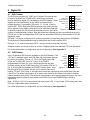
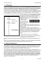
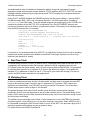
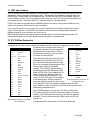
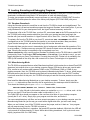
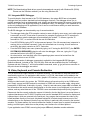
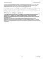
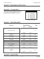
TS-2200 User’s Manual
TS-2200 User’s Manual
Technologic Systems
05
Technologic Systems, Incorporated
16525 East Laser Drive
Fountain Hills, AZ 85268
480-837-5200
FAX 837-5300
[email protected]
http://www.embeddedx86.com/
This revision of the manual is dated
May 21, 2009
All modifications from previous versions are listed in the appendix.
Copyright © 1998-1999 by Technologic Systems, Inc. All rights reserved.
ii
05/21/2009
TS-2200 User’s Manual
Technologic Systems
Limited Warranty
Technologic Systems warrants this product to be free of defects in material and workmanship for a
period of one year from date of purchase. During this warranty period Technologic Systems will repair
or replace the defective unit in accordance with the following instructions:
•
Contact Technologic Systems and obtain a Return Material Authorization (RMA) number and a
copy of the RMA form.
•
Fill out the RMA form completely and include it and dated proof of purchase with the defective unit
being returned. Clearly print the RMA number on the outside of the package.
This limited warranty does not cover damages resulting from lighting or other power surges, misuse,
abuse, abnormal conditions of operation, or attempts to alter or modify the function of the product.
This warranty is limited to the repair or replacement of the defective unit. In no event shall
Technologic Systems be liable or responsible for any loss or damages, including but not limited
to any lost profits, incidental or consequential damages, loss of business, or anticipatory profits
arising from the use or inability to use this product.
Repairs made after the expiration of the warranty period are subject to a flat rate repair charge and
the cost of return shipping. Please contact Technologic Systems to arrange for any repair service.
iii
05/21/2009
TS-2200 User’s Manual
Technologic Systems
Table Of Contents
LIMITED WARRANTY ........................................................................................................................................ III
1
INTRODUCTION......................................................................................................................................... 5
2
PC COMPATIBILITY ................................................................................................................................... 5
3
POWER ...................................................................................................................................................... 5
4
MEMORY .................................................................................................................................................... 6
4.1
4.2
4.3
4.4
5
6
7
8
9
10
11
12
13
DRAM .................................................................................................................................................................... 6
Flash...................................................................................................................................................................... 6
Flash Expansion..................................................................................................................................................... 6
Battery-Backed SRAM ............................................................................................................................................ 6
SERIAL PORTS .......................................................................................................................................... 7
5.1
5.2
5.3
5.4
5.5
Serial Port Configuration Registers ......................................................................................................................... 7
Serial Port Hardware .............................................................................................................................................. 7
RS-485 / RS-422 Support ....................................................................................................................................... 7
Automatically Enabled RS-485 ............................................................................................................................... 8
Adding Serial Ports................................................................................................................................................. 9
DIGITAL I/O .............................................................................................................................................. 10
6.1
6.2
DIO1 Header ........................................................................................................................................................ 10
DIO2 Header ........................................................................................................................................................ 10
LCD INTERFACE ...................................................................................................................................... 11
10BASE-T ETHERNET PORT................................................................................................................... 11
REAL TIME CLOCK .................................................................................................................................. 12
WATCHDOG TIMER................................................................................................................................. 12
LED AND JUMPERS ................................................................................................................................. 13
PC/104 BUS EXPANSION......................................................................................................................... 13
LOADING AND EXECUTING PROGRAMS ............................................................................................... 14
13.1 Zmodem Downloads............................................................................................................................................. 14
13.2 Manufacturing Mode ............................................................................................................................................. 14
13.3 Integrated BIOS Debugger.................................................................................................................................... 15
14 VIDEO, KEYBOARD, AND CONSOLE REDIRECTION ............................................................................. 15
15 FEEDBACK AND UPDATES TO THE MANUAL........................................................................................ 16
APPENDIX A - BOARD DIAGRAM AND DIMENSIONS..................................................................................... 17
APPENDIX B - JP JUMPER BLOCK.................................................................................................................. 17
APPENDIX C - SYSTEM MEMORY MAP .......................................................................................................... 17
APPENDIX D - SYSTEM I/O MAP ..................................................................................................................... 17
APPENDIX E - BIOS INTERRUPT FUNCTIONS ............................................................................................... 18
Int 15h / Function B000h - Technologic Systems BIOS information................................................................................ 18
Int 15h / Function B010h - LED Control ......................................................................................................................... 19
Int 15h / Function B042h – Alphanumeric LCD Support ................................................................................................. 19
APPENDIX F - USING A 12.5 MHZ BAUD CLOCK............................................................................................ 19
APPENDIX G - DIRECT CONTROL OF THE 386EX DIO PINS......................................................................... 20
APPENDIX H - FURTHER REFERENCES ........................................................................................................ 21
APPENDIX I - MANUAL REVISIONS................................................................................................................. 21
iv
05/21/2009
TS-2200 User’s Manual
Technologic Systems
1 Introduction
The model TS-2200 is a compact, full-featured PC compatible Single Board Computer based on the
386EX processor. If you are coming up from the 8-bit microcontroller world, you will find that this
product provides much more performance and much quicker development since you can now use
standard PC development tools such as Turbo C or Quick Basic. If you have done work in the PC
world in the past, you will find you can now build applications for a very small target that does not
require a keyboard, video, floppy disks, or hard drives.
You can typically write and debug code on a host PC using standard development tools for the PC
platform, then simply copy it to and run it on the TS-2200 without modification. If additional peripherals
are required, the PC/104 expansion bus allows for many standard functions available off-the-shelf. It
is also very simple to create a custom PC/104 daughter board for those special features that
differentiate your product. Technologic Systems can provide technical support as well as a free
quotation for any custom hardware, software, or BIOS modifications you may require.
This manual is fairly short. This is because for the most part, the TS-2200 is a standard 80386 based
PC compatible computer, and there are hundreds of books about writing software for the PC platform.
The purpose of this manual is documenting where the TS-2200 differs from a standard PC.
2 PC Compatibility
PC compatibility requires much more than just a 386 processor. It requires PC compatible memory
and I/O maps as well as a PC compatible BIOS. The General Software EMBEDDED BIOS offers a
high degree of compatibility with past and present BIOS standards allowing it to run off-the shelf
operating systems and application software.
The EMBEDDED BIOS has been tested with all major versions of DOS, including MS-DOS, DR-DOS,
and Embedded DOS 6-XL; all major versions of OS/2, including MS-OS/2 and IBM OS/2; MSWindows 3.1, Windows-95, Windows NT, and NetWare 386.
Technologic Systems Embedded PCs are compatible with a wide variety of x86 based
operating systems. A partial list OSes currently used with our boards by customers includes:
• GNU/Linux, kernel versions 1.0.x, 2.0.x, and 2.2.x
• TNT Embedded Toolsuite, Phar Lap Software
• RTKernel, On Time Software
• RTEMS, On-Line Applications Research Corporation
• DOS with Waterloo TCP (WATTCP), public domain TCP/IP source code for DOS
3 Power
The TS-2200 requires regulated +5VDC at 650mA (typical). A quick release screw-down terminal
block for the +5V power and power GND connections is provided for easy connection to an external
power supply.
When power is first supplied to the TS-2200, the board mounted LED (labeled D2) is immediately
turned on under hardware control. Once the processor begins execution, the LED is turned off under
software control. If the LED does not turn on at all, the most likely problem is the power supply. Check
that the +5V and GND connections are not reversed. A diode protects the board against damage in
such a situation, but it will not run.
Please note that supply voltages over +6VDC may damage the TS-2200. Be sure to use a regulated
+5VDC power supply.
5
05/21/2009
TS-2200 User’s Manual
Technologic Systems
4 Memory
4.1 DRAM
The TS-2200 has a total of 2 Megabytes of DRAM providing 640 KB of base memory, 1 Megabyte of
extended memory, and 128 KB of shadow RAM for the BIOS and DOS-ROM. This is identical to a
standard PC memory map. The Flash SSD is the exception -- see below for details.
As shipped, the 1 Megabyte of extended memory is used as a RAM disk by the vdisk.sys device
driver. The RAM disk is accessible as drive C: if the DiskOnChip Flash disk is not installed, drive D: if
it is. The size of the disk can be reduced to provide extended memory for an application (or simply
removed entirely) by editing the CONFIG.SYS file in the root directory of drive A:.
4.2 Flash
There is a total of 1 MB of Flash memory on the TS-2200. The top 128 KB of Flash are reserved for
the BIOS and DOS-ROM. During POST, they are copied from Flash into DRAM at addresses E0000h
through FFFFFh for improved performance (a standard technique known as BIOS Shadowing). The
remainder of the Flash memory (896 KB) is used by a SSD (solid state disk) appearing as drive A.
The SSD is fully supported by the BIOS as an INT 13h drive.
The physical Flash memory is accessed by the BIOS through a 64 KB memory mapped window at
addresses D0000h through DFFFFh. If you are installing a PC/104 daughter card that uses memory
mapped I/O, it must not conflict with this address range.
The Flash memory is guaranteed capable of a minimum of 100,000 write/erase cycles. This means
that if you completely erase and rewrite the SSD drive 10 times a day you have over 27 years before
any problems would occur. Reading the SSD produces no wear at all.
4.3 Flash Expansion
If 896 KB of Flash is insufficient for your application, an empty 32-pin socket is available for Flash
expansion using an M-Systems DiskOnChip 2000 or DiskOnChip Millennium Flash Drive. This product
is a wonder of miniaturization; it is a complete Flash SSD in a single 32 pin package currently
available in sizes from 4 MB up to 144 MB. The DiskOnChip is available from Technologic Systems
as well as other distributors. It is compatible with DOS as shipped, and drivers for other operating
systems are available.
When using the DiskOnChip, it will simply appear as drive C: The DiskOnChip is accessed through an
8 KB range of CE000h through CFFFFh in memory space. If you are installing a PC/104 daughter
card that uses memory mapped I/O, it must not conflict with this address range if the DiskOnChip is
installed. Additionally, the DiskOnChip firmware uses approximately 20 KB of user RAM (below 640
KB).
4.4 Battery-Backed SRAM
The 32-pin socket can also optionally hold 32 KB of battery-backed CMOS SRAM memory. This or the
DiskOnChip may be installed, but not both.
Battery backed SRAM provides non-volatile memory with unlimited write cycles and no write time
degradation, unlike Flash memory. The SRAM uses an additional 32 KB range of C8000h through
CFFFFh. If the SRAM is installed, PC/104 daughter card that uses memory mapped I/O must not
conflict with this address range.
The SRAM can be utilized as a RAM disk (drive C:) by the TSRAMDSK.SYS device driver. The device
driver can be added or removed (and the SRAM accessed directly) by editing the associated line in
the CONFIG.SYS file in the root directory of drive A:. Please see the BIOS/DOS User's Manual for
further information on TSRAMDSK.SYS.
6
05/21/2009
TS-2200 User’s Manual
Technologic Systems
I/O 75h, bit 0 can be read to determine whether the SRAM option is installed; a ‘1’ in bit 0 indicates
that it is installed, a ‘0’ that it is not.
5 Serial Ports
The two PC compatible asynchronous serial ports provide a means to communicate with external
serial devices such as printers, modems, etc. Each is independently configured as a standard PC
COM port which is compatible with the National Semiconductor NS16C450. COM1 appears in the I/O
space at 3F8h – 3FFh and uses IRQ4. COM2 is located at 2F8h – 2FFh and uses IRQ3.
The COM ports use a master clock of 1.8519 MHz as compared to a standard clock of 1.8432 MHz.
This results in an error for all baud rates of .0047 (less than ½%). The error is insignificant and this
clock value allows standard baud rate selections -- for example a divisor of 12 yields 9600 baud.
By changing an internal configuration register in the 386EX, the serial clock can be switched to 12.5
MHz (the processor clock divided by 2). This feature allows baud rates higher than 115 Kbaud (up to
781 Kbaud), as well as low error, non-standard lower baud rates (such as 24 Kbaud). See Appendix F
for further information.
The COM ports may also be configured to use a DMA channel, which is handy when very high baud
rates are being used. When enabled, a DMA request is issued any time a serial port’s receive buffer is
full or its transmit buffer is empty. This allows higher speed operation with much lower CPU overhead.
See the Intel 386EX User's Manual for further details.
5.1 Serial Port Configuration Registers
Because both serial ports are 100% PC compatible, software written for the PC that accesses serial
ports directly or through standard BIOS calls will work without modification on the TS-2200. The
details of the COM port internal registers are available in most PC documentation books or the data
sheet for the National Semiconductor NS16C450 may be consulted.
5.2 Serial Port Hardware
Each serial port has 4 lines buffered: the two data lines
and the CTS / RTS handshake pair. This is quite sufficient to interface with the vast majority of serial devices.
The serial lines are routed to 10 pin headers labeled
COM1 and COM2. A serial adapter cable can be
plugged into the header to convert this into a standard
DB9 male connector. The pin out for the 10 pin header
and DB9 male connector are listed below. The RTS
signal also drives the DTR pin on the serial ports; DTR
is always the same state as RTS. In addition, RTS is
also used to enable the RS-485 transmitter (see below
for more details).
[in]
[out]
NC
NC
CTS
RTS
NC
10
9
8
7
6
5
4
3
2
1
GND
DTR (RTS) [out]
TX data
[out]
RX data
[in]
NC
Figure 1 - Serial Port Header and DB9 Pinout [signal direction is in brackets]
PLEASE NOTE: The serial port headers
use a non-standard numbering scheme.
This was done so the header pins would
have the same numbering as the corresponding DB-9 pin; i.e. pin 8 (CTS) on the
header connects to pin 8 on the DB-9
5.3 RS-485 / RS-422 Support
An option is available to add support to COM1 for half or full-duplex RS-485. RS-485 drivers allow
communications between multiple nodes up to 4000 feet (1200 meters) via twisted pair cable. Halfduplex RS-485 requires one twisted pair plus a Ground connection, while full-duplex RS-485 (also
known as RS-422) requires two twisted pairs plus a Ground connection.
For half-duplex operation, a single twisted pair is used for transmitting and receiving. The serial port's
RTS signal controls the RS-485 transmitter/receiver (see next section for automatic operation). When
RTS is asserted true (bit 1 of the modem control register = 1), the RS-485 transmitter is enabled and
the receiver disabled. When RTS is de-asserted the transmitter is tri-stated (disabled) and the receiver
is enabled. Since the transmitter and receiver are never both enabled, the serial port UART does not
receive the data transmitted. The transmitter and receiver share a single pair of signals that are
05/21/2009
7
TS-2200 User’s Manual
Technologic Systems
available in a screw-down terminal block. See the table below for pin-outs Note: the correct jumper
must be installed. See the next table for details.
Position (with terminal strip facing you)
Left
Center
Right
Silk-screen Label
TX+
TX-
GND
RX-
RX+
Half-duplex Usage
TX+ / RX+
TX- / RX-
GND
Not Used
Not Used
Full-duplex Usage
TX+
TX-
GND
RX-
RX+
Table 1 - RS-485 Signals
For full duplex (RS-422) operation, a twisted pair is used for
receiving and another twisted pair is used for transmitting.
The RS-485 transmitter is typically enabled continuously
(RTS asserted), since the separate transmit and receive
twisted pairs remove problems with data loop-back. The
full-duplex receiver inputs are available on the terminal
block (see the table above). Note: the correct jumper must
be installed - see the table below for details.
Fail-safe bias resistors are used to bias both the TX pair
and the RX pair to the correct state when these pairs are
not being actively driven. This is an important consideration,
since in a typical RS-485 installation, the drivers are
frequently tri-stated. If fail-safe bias resistors are not
present, the 485 bus will be floating and very small amounts
of noise can cause spurious characters at the receivers. A
1.2 KOhm resistor is used to pull the TX+ signal to 5V and
another 1.2 KOhm resistor pulls the TX- signal to ground.
The RX+ and RX- signals are biased in the same manner.
Termination resistors are also required for reliable
operation particularly when running long distances.
Termination resistors should only be installed at each end
of a RS-485 transmission line pair. In a multi-drop
application where there are several drivers and/or receivers
attached, only the devices at each end of the
transmission line pair should have termination
resistors.
RS-485 Quick start procedure:
1. The RS-485 option must be
installed
2. Install JP6 or JP7 to enable Half or
Full duplex RS-485 operation
3. Attach the RS-485 cable to the 5pin terminal strip connector.
4. Set the COM1 UART serial
parameters (baud rate, data, parity,
and stop bits, interrupts, etc).
5. To transmit data, assert RTS and
write the data to the UART
6. To receive data, deassert RTS and
read the data from the UART
Jumper
JP6
JP7
neither
Table 3 - COM1 Receiver Source
I/O
Installing JP4 adds a 100 Ohm termination resistor to
the RX pair while JP5 adds a 100 Ohm termination
resistor to the TX pair.
When the RS-485 option is installed, jumpers JP6 and
JP7 select which receiver is fed to the COM1 UART.
Only one (or neither) of these jumpers should be
installed at a time!
A read at I/O location 76h bit 0 will return a "1" when
the RS-485 option is installed.
Receiver Source
Full-duplex RS-485
Half-duplex RS-485
RS-232
R/W
Address
76h
Read
76h
Write
Bit 0 Description
RS-485 option
0 = Not installed
1 = Option installed
RS-485 control
0 = use RTS enabled RS-485
1 = enable automatic RS-485
77h
Read
Returns status of TX485EN pin
Table 2 – TS-2100 Control Registers – All signals
are R/W through bit 0 of the address
5.4 Automatically Enabled RS-485
In most RS-485 applications, the transmitter is enabled while sending data and disabled (tri-stated)
when not. This allows for an inexpensive 'network' of multiple devices, all using a single twisted pair to
communicate. Enabling and disabling the RS-485 transmitters can be done in software by asserting
and deasserting RTS. This can be difficult to implement and bug prone.
8
05/21/2009
TS-2200 User’s Manual
Technologic Systems
A simpler method implemented on the TS-2200 utilizes Timer 2 in the i386EX to keep track of the bits
shifting out of the UART. It automatically turns on the transmitter, waits for the character to be sent,
then turns off the transmitter. The timer is simply initialized once based on baud rate and data format.
This totally eliminates the software overhead of controlling the RTS line manually.
To activate automatic transmitter enable, I/O location 76h bit 0 must be set to a "1", and Timer 2
initialized. When I/O location 76h bit 0 is set to "0", user software uses the RTS line to control the
RS-485 transmitter. (Set RTS, and the transmitter is enabled. Clear RTS, and it is disabled.)
To initialize Timer 2, a value of 0B2h must be written to I/O location 043h, then a 16 bit count must be
written to I/O location 042h as two consecutive bytes with least significant byte first. The count is
determined by the following equation:
Count = [16 * (Baud Divisor) * (Bits/Character)] - 2
For example, for 9600 baud, 8 data, no parity, 1 stop bit:
Baud divisor = 12
Bits/Character = 1 start bit + 8 data bits + 0 parity bits + 1 stop bit = 10
Count = [16 * 12 * 10] - 2 = 1918 decimal = 077Eh
The instructions in x86 assembly would then be:
MOV
OUT
MOV
OUT
MOV
OUT
AH, 0B2h
043h, AH
AH, 07Eh
042h, AH
AH, 07h
042h, AH
; Set timer2 mode to one-shot
; load timer2 LSB
; load timer2 MSB
Serial Format
9600, No parity, 8 Data, 1 Stop
Formula
[16 * 12 * 10] - 2 =
Result (decimal)
1918
MSB
07h
LSB
7Eh
19200, No parity, 7 Data, 1 Stop
[16 * 6 * 9] - 2 =
862
03h
5Eh
9600, Even parity, 8 Data, 2 Stop
[16 * 12 * 12] - 2 =
2302
08h
0FEh
2400, Space parity, 8 Data, 1 Stop
[16 * 48 * 11] - 2 =
8446
20h
0FEh
Table 4 - Auto Enabled RS-485 Examples
Note: These equations assume the standard 1.85 MHz clock is being used for baud rate generation. If
the 12.5 MHz clock is being used (see Appendix F) these equations must be modified. Contact
Technologic Systems for details.
5.5 Adding Serial Ports
If your project requires more than two serial ports, additional ports may be added via the PC/104
expansion bus. Technologic Systems currently offers a 2 serial / 1 parallel port card, and other
manufacturers sell cards with up to four additional serial ports. Typically these would be configured as
COM3 or COM4 or be assigned other non-standard I/O locations. Because DOS only directly supports
four serial ports, any additional ports beyond four will require software drivers.
The PC/104 bus has IRQ3, 4, 5, 6, 7 or 9 available for additional serial ports. If IRQ3 or 4 are to be
used on a PC/104 expansion card, then care must be taken since COM2 and COM1 also use these
IRQs, respectively. For example, if IRQ4 is used for COM3 then either COM1 must be used in a noninterrupt fashion or only one COM port can have the interrupt enabled at a time. In any case only one
COM should have the Interrupt Enable (Bit 3 of Modem Control Reg.) set at any one time if they share
the same IRQ. This is a standard issue with the PC architecture. A better solution is to simply use
interrupts other than 3 or 4 for additional serial ports.
9
05/21/2009
TS-2200 User’s Manual
Technologic Systems
6 Digital I/O
6.1 DIO1 Header
P3.2 14 13 IRQ5 / P3.3
The DIO1 port provides +5V, GND, and 12 digital I/O lines that may
IRQ4
/
P3.0
12 11 IRQ3 / P3.1
be used to interface the TS-2200 with a wide range of external
DTR2
/
SRXCLK
10
9 RI2 / SRXD
devices. Additional digital I/O is available on the DIO2 header. These
DSR2 / STXCLK 8
RTS2 / STXD
7
signals are connected directly to the 386EX and several have
IRQ7 / P3.5 6
P1.0
5
multiple functions. For example, DIO pins 6, 11, 12, and 13 are by
P1.5 4
3 P3.6
default IRQ7, IRQ3, IRQ4, and IRQ5 respectively. By setting configuGND 2
1 5V
ration registers in the 386EX, these pins can be individually changed
Figure 2 – DIO1 Header Pinout
to general purpose I/O (GPIO) as high-impedance inputs, open-drain
outputs, or complementary outputs. Note that these same signals are also connected directly to the
PC/104 bus; if a pin is configured as GPIO, then the associated IRQ will not be available for PC/104
expansion cards.
DIO pins 7-10 can be configured as a synchronous serial port supporting baud rates to 6.25Mbaud.
These pins are COM2 handshake lines by default that can be also used as GPIO.
DIO pins 3, 4, 5, and 14 are always GPIO – they do not have secondary functions.
All digital outputs can source or sink up to 8mA. All digital inputs have standard TTL level thresholds.
For further information on configuration and use of these pins, See Appendix G.
6.2 DIO2 Header
P1.3 14 13 IRQ6 / P3.4
Up to 13 additional DIO lines are available on the DIO2 Header. Pins
TX485EN 12 11 LinkLED#
1,3,5,and 7 are digital inputs with 10K Ohm pull-up resistors that can
DCD2 10 9 RxLED#
be read at I/O location 77h bits 1-4. Pin 4 is a Digital output that
RTS1 / P1.1 8
7 IN1@77
drives the TS-2200 LED. Pins 6,8,13,and 14 are i386EX
P1.2 6
5 IN2@77
programmable I/O lines. Pin 10 is a fixed input that can be read
LED-ON 4
3 IN3@77
(inverted polarity) at the COM2 Status Reg. (I/O location 2FEh bit 7).
GND 2
1 IN4@77
Pin 12 is the signal that enables the RS-485 Transmit driver. If the
Figure 3 – DIO2 Header Pinout
RS-485 option is not installed, this pin can be read as input at I/O
location 77h bit 0. Pins 9 and 11 are open-drain active-low outputs that drive the Ethernet Link and
LAN LEDs. The default configuration is for these to be driven by the Ethernet controller to indicate
network presence and activity. These can be reprogrammed to be general-purpose outputs. For more
information regarding these 2 lines, please consult the Cirrus Logic CS8900A Users Guide in
Appendix H.
Note – DIO2 pin 14 (P1.3) is also shared with user jumper JP3. If user jumper JP3 is being used, then
DIO2 pin 14 should be left not connected.
For further information on configuration and use of these pins, See Appendix G.
10
05/21/2009
TS-2200 User’s Manual
Technologic Systems
7 LCD Interface
A 14-pin LCD connector is provided on the TS-2200 for interfacing with standard alphanumeric LCD
displays. These displays use a common controller, the Hitachi HD44780 or equivalent. While software
written for the HD44780 will work with all displays using the controller, the cable needed is dependent
on the display used. For most displays, a straight-through type ribbon cable can be used. The
connector on the LCD display is typically mounted on the backside of the display. Warning – using an
incorrect cable or mounting the LCD connector on the front-side can result in a reverse power polarity
and can damage the LCD display. Please refer to your LCD data sheets for in-depth information.
The TS-2200 BIOS incorporates a fairly complete set of INT10h video routines that work with the LCD.
Once the LCD has been enabled (INT15h/Func B042h –
Pin
Function
Comments
see 0 below) the LCD can be written to using the
1
LCD 5V
standard BIOS routines. This includes the majority of PC
languages, such as C and C++. See the programs
2
LCD GND
included on the utility
3
Reg. Select Buffered A0
disk for examples.
2 4 6 8 10 12 14
4
Bias
470 Ohm to GND
5
LCD Enable
Active high
6
Write#
Active low
7
D1
8
D0
1 3 5 7 9 11 13
I/O addresses 72h and
Figure
4 - LCD Header Pinout
73h are used to access
the LCD. Figure 4
shows the header pin-out, while Table 5 lists the LCD
signals. The section below will briefly describe the LCD
interface signals.
9
D3
10
D2
11
D5
D0 – D7: Buffered
bi-directional data bus
12
D4
13
D7
The register select signal is simply the buffered A0
address line. Thus, reads and writes to 72h cause register
select to be low, and those to 73h cause it to be high.
Generally the LCD uses this line to separate data bytes
from command bytes. See your LCD data sheet for
details.
14
D6
The /Write signal is an active low write enable line.
Table 5 - LCD Header Signals
LCD Select is an active high signal, raised whenever the
LCD addresses are being read or written.
D0 – D7 are bi-directional, buffered copies of the data bus and carry all data and commands to the
LCD.
Table 4 is not the standard pin-outs given for LCD displays. But this pin-out allows a standard ribbon
cable to be used when the ribbon cable is attached to the backside of the LCD.
8 10Base-T Ethernet Port
The TS-2200 has full-function IEEE 802.3 Ethernet capability (10 Mbit/sec) provided by a Cirrus Logic
CS8900A Ethernet controller. The CS8900A is a single-chip, 16-bit Ethernet controller that includes
such features as full-duplex operation, power saving shutdown modes, and LED indicators for link
status and activity. The physical interface is 10Base-T (RJ45 connector).
The TS-2200 has both a LINK LED and a LAN LED that indicates the current ethernet status. The
LINK LED (labeled D4) is active when valid ethernet link pulses are detected. This LED should be ON
whenever the TS-2200 is powered on and properly connected to a 10BaseT Ethernet network. The
LAN LED (labeled D3) should pulse ON briefly when any network traffic is detected. This includes all
traffic, not just that sent to or from the TS-2200. Both of these LEDs are controlled by the CS8900A
and do not require initialization. Additionally, the LEDs can be placed under software control, allowing
the customer application use of the LEDs for feedback. Please see the CS8900A User Manual,
Appendix H, for further details.
11
05/21/2009
TS-2200 User’s Manual
Technologic Systems
A standard packet driver is installed on the board by default, along with a few sample network
applications written with the public domain Waterloo TCP/IP software (WATTCP). WATTCP is a freely
available package (including source code) that provides TCP/IP connectivity for programs written for
the DOS environment.
During POST, the BIOS initializes the CS8900A registers with the correct settings – interrupt IRQ12,
I/O address range 300h – 30Fh, and I/O mapped operation. The DOS packet driver is loaded by
AUTOEXEC.BAT once DOS starts. To run the sample programs (ping and finger) on the TS-2200, first
examine the contents of the WATTCP.CFG configuration file in the A:\ETHERNET directory and
correct any information that is not valid for your particular network. Then simply run a sample program
from the DOS command line. For example:
[A:\]ping www.embeddedx86.com
Technologic Systems Example Configuration
Pinging 'www.embeddedx86.com' [209.130.84.83]
sent PING # 1 , PING receipt # 1 : response time 0.00 seconds
Ping Statistics
Sent
: 1
Received
: 1
Success
: 100 %
Average RTT : 0.35 seconds
[A:\]
If you prefer to use a package other than WATTCP, go right ahead. Device-drivers for other operating
systems and network protocols are available from both the Technologic Systems and Cirrus Logic
web sites (see Appendix H below).
9 Real Time Clock
The Dallas Semiconductor DS12887 is used for the PC compatible battery-backed real-time clock. It is
a completely self-contained module that includes a Motorola 146818 compatible clock chip, the
32.768 kHz crystal, the lithium battery, and 114 bytes of battery-backed CMOS RAM. It is guaranteed
to maintain clock operation for a minimum of 10 years in the absence of power. It is located at the
standard PC I/O addresses of Hex 070 and 071. The top 32 bytes (index 60h through 7Fh) are not
used by the BIOS and are available for user applications.
10 Watchdog Timer
The Intel 386EX contains a 32-bit watchdog timer (WDT) unit that can be used in two different modes
to effect a watchdog supervisory function. In either mode, a system reset is asserted when the WDT
times out preventing a system “hanging” due to a software bug. To prevent a WDT timeout, the
application must periodically “feed” the WDT by writing to specific I/O locations. The 32-bit downcounter allows timeout values as high as 160 seconds.
The general-purpose timer mode is more flexible in that the timeout values can be changed
dynamically and the timer can be turned on and off under software control. The disadvantage of this
mode is that it doesn’t provide 100% protection because a bug could turn off the timer during a crash
and the system would hang.
The software secure watchdog mode utilizes a “lockout sequence” to set a WDTEN bit in the watchdog status register. Once this bit is set, only a system reset can clear this bit. When WDTEN is set, it
is not possible to change the WDT timeout value or to turn off the WDT. This provides a high level of
assurance against errant software causing a system to hang.
For details see the Intel 386EX User Manual.
12
05/21/2009
TS-2200 User’s Manual
Technologic Systems
11 LED and Jumpers
The TS-2200 has three LEDs available for user software. The user LED (labeled D2) can be used for
diagnostics, status messages, and simple output. This signal is also available as a digital output on
the DIO2 port. When power is first supplied to the TS-2200, the user LED is immediately turned on
under hardware control. Once the processor begins execution, the LED is turned off, then flashed on
and off again briefly. After boot, this LED is reserved solely for user applications.
LEDs D3 and D4 are controlled by the CS8900A Ethernet Controller, and provide feedback on the
status of the network. See Section 8 above for details.
If the user LED does not turn on at all when power is applied, the most likely problem is the power
supply. Check that the +5V and GND connections are not reversed. A diode protects the board
against damage in such a situation, but it will not run.
BIOS interrupt functions are used to interface software with the user LED and option jumper JP3.
Please see Appendix C for further details and the utility disk for example code.
12 PC/104 Bus Expansion
The PC/104 is a compact implementation of the PC/AT ISA bus ideal for embedded applications.
Designers benefit from using an already-developed standard, rather than creating their own. Further,
the presence of a compact form-factor PC
Pin #
Signal Name
Pin #
Signal Name
compatible standard has encouraged the
A1
IOCHCHK#
A2 - A9
D7 through D0
development of a broad array of off-theB5
-5V
A10
IOCHRDY
shelf products, allowing a very quick time
B6
DRQ2
A11
EN
to market for new products.
B7
-12V
A12 - A31
A19 through A0
A32
GND
B1
GND
B2
RESETDRV
B3
+5V
B4
IRQ9
B11
SMEMW#
B12
SMEMR#
B13
IOW#
B14
IOR#
B20
SYSCLK (8.33 MHz)
B21
IRQ7 †
B22
IRQ6 †
B23
IRQ5 †
B24
IRQ4 †
B25
IRQ3 †
B28
BALE
B29
+5V
B30
OSC
B31
GND
B32
GND
Table 6 - Supported PC/104 Signals
† these signals are also connected
to the DIO port.
B8
ENDXFR#
The electrical specification for the PC/104
B9
+12V
expansion bus is identical to the PC ISA
B15
DACK3# ‡
bus. The mechanical specification allows
B16
DRQ3 ‡
for the very compact implementation of the
B17
DACK1#
ISA bus tailor made for embedded
B18
DRQ1
systems. The full PC/104 specification is
B19
REFRESH#
available from the IEEE Standards Office
B26
DACK2#
under # IEEE P996.1 (see Appendix E for
B27
TC
further information). Basically, this bus
Table 7 - Unsupported PC/104
allows multiple daughter boards in a 3.6
Signals
inch by 3.8 inch form factor to be added in
‡ PC/104 expansion cards must not
a self-stacking bus. Since the electrical
connect to these pins.
specs are identical (except for drive levels)
to a standard PC ISA bus, standard peripherals such as COM
ports, Ethernet, video, LCD drivers, and Flash drives may be easily
added using standard drivers.
The TS-2200 implements a sub-set of the 8-bit version of the
PC/104 bus. We have found this allows the support of the vast
majority of PC/104 boards including all of the above mentioned
examples. The one feature missing is DMA, which few PC/104
boards use.
See Appendix A for information on PC/104 pin numbering
13
05/21/2009
TS-2200 User’s Manual
Technologic Systems
13 Loading, Executing and Debugging Programs
Two methods are available for transferring files between a desktop PC and your TS-2200: Zmodem
downloads, and Manufacturing Mode. Full descriptions of each are detailed below.
To make your program automatically execute at power up, just edit the AUTOEXEC.BAT file on the
Flash SSD drive and replace the name of the factory test program (EPC-DIAG.EXE) with yours.
13.1 Zmodem Downloads
Using the Zmodem protocol to send files to and from the TS-2200 is simple and straightforward. The
only requirement is a terminal emulation program that supports Zmodem, and virtually all do. If you are
using Windows 9X for your development work, the HyperTerminal accessory works well.
To download a file to the TS-2200 from your host PC, execute DL.BAT at the DOS command line on
the TS-2200 (while using console-redirection from within your terminal emulator) and begin the
transfer with your terminal emulator. In HyperTerminal, this is 'Send File...' from the 'Transfer' menu.
To upload a file from the TS-2200 to your host PC, execute UL.BAT <FILENAME> at the DOS
command line on the TS-2200 and start the transfer in your terminal emulator. Many emulators,
HyperTerminal among them, will automatically begin the transfer themselves.
Occasionally there may be errors in transmission due to background solid state disk operations. This
is not a problem -- Zmodem uses very accurate CRC checks to detect errors and simply resends bad
data. Once the file transfer is complete the file is completely error free.
Please note that the utility used to perform Zmodem file transfers on the TS-2200 side is called DSZ,
produced by Omen Technologies. DSZ is shareware -- it is not free. If you decide to use it, you are
legally obligated to pay Omen Technologies. Currently the cost is $20. Further info is available in the
DSZ zip file located on the utility disk, and contact info for Omen Technologies is in Appendix E.
13.2 Manufacturing Mode
The TS-2200 has a special feature called 'Manufacturing Mode' which makes the on-board Flash SSD
appear as just another drive on your desktop computer using a DOS device driver and a serial cable.
First, connect a null modem cable between COM2 on the TS-2200 and COM1 or COM2 of your
desktop computer. Next, the TS-2200 must be placed in Manufacturing Mode. To do so, install jumper
JP1 and power cycle the unit. Manufacturing Mode will automatically start once the POST routines
have been executed. At this point, the TS-2200 will simply sit and wait for serial packets to arrive from
a host.
Now install the Manufacturing Mode driver on your desktop computer. To do so, simply copy the
MFGDRV.SYS device driver from the utility disk to anywhere on your desktop machine's hard drive.
Then insert the following line in your CONFIG.SYS file and reboot:
DEVICE=<PATH>\MFGDRV.SYS /UNIT=0 /BAUD=38K /PORT=COMX
Where <PATH> is the full path to the location where you copied the MFGDRV.SYS driver, and X is the
port on your host PC that the null modem cable is connected to (1 or 2).
The Flash SSD drive should now appear on the next free drive letter on your desktop computer
(usually the D: or E: drive). Simply copy your program onto the drive, and that's it!
You can create directories, edit files, and even execute programs on your desktop computer over the
Manufacturing Mode link just the way you would with a regular disk drive, just a bit more slowly.
When you are finished, turn off the TS-2200, remove the jumper, and turn it back on. Your program
will now execute every time the TS-2200 is turned on.
While Manufacturing Mode is in operation, the board LED provides feedback. While idle, the LED will
cycle on and off at approximately 1/2 Hertz. While data is being transferred, it will cycle much more
rapidly (anywhere from 5 to 1000 Hertz)
14
05/21/2009
TS-2200 User’s Manual
Technologic Systems
NOTE: The Manufacturing Mode driver currently does not work correctly with Windows 9X (95/98).
Please use the Zmodem method if you are using Windows 9X.
13.3 Integrated BIOS Debugger
To provide simple, direct access to the TS-2100 hardware, the system BIOS has an integrated
debugger that can perform standard low-level debugger functions. The debugger allows you to
perform operations such as disassemble code, display and alter the contents of memory, write to and
read from I/O ports, and single-step through or breakpoint code. The debugger is not intended for use
as the only debugging tool for applications, but it can be a real lifesaver when you need interactive,
direct access to hardware.
The BIOS debugger can be entered by any of several methods:
•
The debugger hooks the CPU exception vectors in case a divide by zero occurs, an invalid opcode
is executed, or an INT 3 instruction is executed, for example. By placing an INT 3 instruction in
your application code the debugger will automatically be invoked. To resume, type the 'G'
command to "GO", or continue on with the rest of initialization.
•
From DOS-ROM by typing ‘INT3’ at the command prompt. If the full command.com interpreter is
running, this is an internal command. If only mini-command.com is running, this will execute a
small utility that simply contains an ‘INT 3’ instruction.
•
From the BIOS Setup main menu (started by typing ‘ctrl-C’ during the BIOS POST), the ENTER
SYSTEM BIOS DEBUGGER selection will enter the debugger. After use, typing the ‘G’ (go)
command will return to the SETUP screens.
•
As a boot action, as a last-ditch effort if the operating system cannot be booted from the
appropriate drives or out of ROM.
A complete discussion of debugger commands is available in the Integrated BIOS Debugger
Reference Manual, included on the TS-2100 Utility Disk and also available from the Technologic
Systems web site. Entering ‘?’ will list all available commands, and a ‘g’ (go) will return execution to
the point where the debugger was called.
14 Video, Keyboard, and Console Redirection
The TS-2200 has no video controller or keyboard interface. This was done to keep the board size
small and the cost low. For applications that require it, a PC/104 video board can be added to the
system easily. This could be a VGA controller, graphic LCD interface, or a custom board of your own
design.
Without a video board in the system, the TS-2200 redirects all console activity to the COM2 serial
port. Simply connect an ANSI terminal (or emulator) to COM2 with a null modem cable, using serial
parameters of 9600 baud, 8 data bits, no parity, 1 stop bit, and make sure jumper JP2 is installed. All
text information that would normally be displayed on a video screen is now displayed in your terminal
window, and any serial data sent to the TS-2200 is seen as standard keyboard input by programs.
Please note that the console redirection support is limited by the fact that there is no actual video or
keyboard hardware on the TS-2200. Programs must use the standard BIOS routines for display and
keyboard input, which are rerouted to the serial port. Any program that accesses the video or keyboard hardware directly will not work. Keyboard redirection is limited simply because most of the
extended keys on the keyboard (function keys and Alt key in particular) are not sent by the terminal
emulator. For these reasons, the console redirection feature is meant more for system development,
testing, and field repair, rather than as the primary user interface for a finished product.
If your application uses COM2, removing the jumper JP2 easily disables console redirection.
15
05/21/2009
TS-2200 User’s Manual
Technologic Systems
If you wish to use a different serial port and / or baud rate for the console, the CONSOLE.EXE utility
allows these modifications to be made. Please see the appropriate application notes for further
details, available on the utility disk or from the Technologic Systems web site.
If a video board is installed on the PC/104 bus, the video BIOS on the graphics card will automatically
replace the standard video routines (INT10h), disabling both the LCD display and the display
redirection (keyboard redirection will continue). If the console redirection jumper JP2 is also removed,
the keyboard redirection is disabled as well.
15 Feedback and Updates to the Manual
To help our customers make the most of our products, we are continually making additional and
updated resources available on the Technologic Systems web site. These include manuals,
application notes, programming examples, and updated software and firmware. Check in periodically
to see what's new!
When we are prioritizing work on these updated resources, feedback from customers (and
prospective customers) is the number one influence. If you have questions, comments, or concerns
about your TS-2200 Embedded PC, please let us know. Details for contacting us are listed in the front
of this manual.
16
05/21/2009
TS-2200 User’s Manual
Technologic Systems
Appendix A - Board Diagram and Dimensions
Currently not available
Appendix B - JP Jumper Block
Table 8 lists all option jumpers and their functions.
These jumpers are clearly labeled on the upper
edge of the board (see Appendix A above).
Jumper
Function
JP1
Manufacturing Mode
JP2
JP3
Console Redirection
User Jumper (P1.3)
JP4
TX485 Term. Res.
JP5
JP6
RX485 Term. Res.
Full Duplex RS-485
JP7
Half-Duplex RS-485
Table 8 - Jumper Listing
Appendix C - System Memory Map
Resource
Starting Address
hex
Size
decimal
Extended Memory (RAM)
1M
100000h
1024k
(Shadow RAM)
F0000h
960k
DOS / BIOS Extension
(Shadow RAM)
E0000h
896k
Solid-state disk drive window
(Flash RAM)
D0000h
832k
PC/104 or DiskOnChip
CE000h
824k
8k
PC/104 or Battery-Backed SRAM
C8000h
800k
24k
C0000h
768k
BIOS
PC/104
(typically video BIOS)
PC/104
64k
64k
64k
32k
128k
(typically video memory)
A0000h
640k
Lower Memory
640k
(RAM)
00000h
00000
Figure 5 – TS-2200 Memory Map
Appendix D - System I/O Map
17
05/21/2009
TS-2200 User’s Manual
Technologic Systems
The following table lists the I/O addresses used by the system. All other I/O locations from 100h
through 3F7h are available on the PC/104 expansion bus.
Hex Address
Resource
F000h - FFFFh
400h – EFFFh
3F8h – 3FFh
Internal 386EX Registers
PC/104 Bus
(Not recommended for use)
COM1
300h – 30Fh
2F8h – 2FFh
80h – FFh
CS8900A Ethernet controller
COM2
Internal 386EX peripherals
074h – 077h
072h – 073h
Board configuration registers
Alphanumeric LCD
070h – 071h
000h – 06Fh
RTC and CMOS memory
Internal 386EX peripherals
I/O
R/W
Address
74h
Read
75h
Read
76h
76h
Bit 0 Description
Always 1
SRAM option
Read
0 = Not installed
1 = Option installed
RS-485 option
Write
0 = Not installed
1 = Option installed
RS-485 control
0 = use RTS enabled RS-485
1 = enable automatic RS-485
77h
Read
Returns status of TX485EN pin
Table 10 – TS-2200 Control Registers – All signals
are R/W through bit 0 of the address
Table 9 – TS-2200 I/O Map
Appendix E - BIOS Interrupt Functions
We have extended the standard BIOS interrupts with several functions that simplify interfacing with
the TS-2200 hardware.
Many books are available with detailed information on using interrupts with just about any language.
Example code is also available on the utility disk.
Int 15h / Function B000h - Technologic Systems BIOS information
This function is mostly for our own internal use, but may be useful for user programs as well. For
example, your program could have debugging code that executes on your desktop machine, but does
not when the program is executing on the TS-2200.
ENTRY:
AX = B000h
EXIT:
CY = 0 (carry flag)
AH = 0
AL = SP_VERSION
For standard versions of the BIOS, this is 0. An 'SP number' is assigned when custom
modifications are made to the BIOS for a client, and it is returned in this register. Contact
us for further information.
BH = BIOS Version, Major Number.
E.g. If the current BIOS version is 1.25, the register will contain 01h.
BL = BIOS Version, Minor Number.
E.g. If the current BIOS version is 1.25, the register will contain 19h (19h = 25 decimal).
CH = Base Flash Memory Size / 512kB
The TS-2200 is available with 1024kB of base Flash memory standard, but this can be
increased to 2048 KB for custom orders. These would be returned as 02h or 04h,
respectively.
CL = 16h
This is the hardware model number (16h = 22 decimal).
DX = 'TS' (5452h)
18
05/21/2009
TS-2200 User’s Manual
Technologic Systems
Int 15h / Function B010h - LED Control
This function is used to turn the board LED on and off. You can also invert the LED, i.e. if the LED is
off, it will be turned on, and if it is on it will be turned off.
ENTRY:
AX = B010h
BH =
00
01
81
- LED off.
- LED on.
- LED invert.
EXIT:
CY = 0 (carry flag)
AH = 0
Int 15h / Function B042h – Alphanumeric LCD Support
This routine enables and disables the console on the LCD interface. It supports all LCD displays sized
2 x 40 or smaller using a Hitachi HD44780 controller.
ENTRY:
EXIT:
AX = B042h
BH = 00
01
02
- Disable LCD
- Enable LCD
- Return current LCD status
CY = Set if error, else clear if success. (carry flag)
AH = 00
- No Error / LCD initialized OK
BH = 00
- LCD currently disabled / Not present
01
- LCD currently enabled and running.
Appendix F - Using A 12.5 MHz Baud Clock
Each serial port baud rate generator clock can be independently switched between either the
standard 1.85 MHz clock or a 12.5 MHz clock (the internal processor clock divided by 2).
Changing the clock to 12.5 MHz allows baud rates higher than 115 kbaud (up to 781 kbaud), as well
as low error, non-standard lower baud rates (such as 24 kbaud).
The baud rate clock is controlled by I/O location 0F836h:
Bit 0 controls COM1.
Bit 1 controls COM2.
Setting a bit to 0 uses the standard 1.85 MHz clock, and setting a bit to 1 uses the 12.5 MHz
processor clock. NOTE: You must not modify the other bits of this register. You must use a readmodify-write procedure to change these bits. The following example in assembly illustrates this:
MOV DX, 0F836
; load the I/O address
IN
AL, DX
; read the configuration register
OR
AL, 00000001b
; switch COM1 to the 12.5 MHz clock
OUT DX, AL
; write the register
Note: If using automatic RS-485, see section 5.4 above.
19
05/21/2009
TS-2200 User’s Manual
Technologic Systems
Appendix G - Direct Control of the 386EX DIO Pins
The Intel386 EX processor has three 8-bit bi-directional I/O ports, all of which are functionally identical
(Figure 16-1). Each port has three control registers and a status register. All three ports share pins
with internal peripherals. Several of these pins are routed to the DIO ports. If your design does not
require a pin’s peripheral function, you can configure that pin for use as an I/O port. For example, if
you don’t need IRQ6 for PC/104, you can use the associated pin (386EX P3.4) as DIO2 pin 13. Each
pin can operate either in I/O mode or in peripheral mode. In I/O mode, a pin has three possible
configurations:
•
high-impedance input
•
open-drain output (requires an external pull-up resistor)
•
complementary output
In I/O mode, register bits control the direction (input or output) of each pin and the value of each
output pin. In peripheral mode, the internal peripheral controls the operation (input or output) of the
pin.
Each port has three control registers and a status register associated with it (). The control registers
(PnCFG, PnDIR, and PnLTC) can be both read and written. The status register (PnPIN) can only be
read. All four registers reside in I/O address space.
Register
I/O Address
P1CFG
P3CFG
0F820h
0F824h
(read/write)
P1DIR
P3DIR
Description
Port n Mode Configuration:
Each bit controls the mode of the associated pin.
0 = Selects I/O mode.
1 = Selects peripheral mode.
0F864h
0F874h
(read/write)
Port n Direction:
Each bit controls the direction of a pin that is in I/O mode. If a pin is in
peripheral mode, this value is ignored.
0 = Configures a pin as a complementary output.
1 = Configures a pin as either an input or an open -drain output.
P1LTC
P3LTC
0F862h
0F872h
(read/write)
Port n Data Latch:
Each bit contains data to be driven on to an output pin that is in I/O mode.
Write the desired pin state value to this register. If a pin is in peripheral
mode, this value is ignored.
Writing a value to a PL bit causes that value to be driven onto the
corresponding pin.
For a complementary output, write the desired pin value to its PL bit. This
value is actively driven high or low onto the pin.
For an open-drain output, a zero results in a actively driven low on the pin,
a one results in a high-impedance (input) state at the pin.
To configure a pin as an input, write a one to the corresponding PL bit. A
one results in a high-impedance state at the pin, allowing external hardware
to drive it.
Reading this register returns the value in the register – not the actual pin
state.
P1PIN
P3PIN
(read only)
0F860h
0F870h
Port n Pin State:
Each bit of this read-only register reflects the state of the associated pin.
Reading this register returns the current pin state value, regardless of the
pin’s mode and direction.
Table 11 – 386EX I/O Port Registers
20
05/21/2009
TS-2200 User’s Manual
Technologic Systems
In the default configuration, P1.5, P1.0 and P3.6 are all initialized as inputs, while P3.0, P3.1, and
P3.3 are initialized as "peripherals" (IRQ4, IRQ3, and IRQ5)
Warning: When changing these registers, always use read/modify/write procedures so that
other port pins (used by on-board peripherals) are not affected.
For example, let's say you want to use 386EX Port 3.1 (DIO1 pin 11) as an output rather than IRQ3
(the default configuration).
1. Read P3CFG (I/O F824h), AND it with 0FDh, write it back to F824h. (changes from peripheral
to I/O pin)
2. Read P3DIR (I/O F874h), AND it with 0FDh, write it back to F874h. (this made it a
complementary output)
3. To set this pin to a "1", Read P3LTC (I/O F872h), OR it with 02h, write it back.
Note: Because the serial ports are internal to the 386EX, COM1 and COM2 can still use IRQ4 and
IRQ3 even when the associated pins P3.1 and P3.0 are configured as DIO pins DIO1.11 and DIO1.12
– the interrupts are simply no longer available on the PC/104 bus.
Appendix H - Further References
Technologic Systems Web Site
http://www.embeddedx86.com/
Crystal CS8900A Ethernet Controller Overview
http://www.cirrus.com/en/products/pro/detail/P46.html
Dallas Semiconductor DS12887 Data Sheet
Intel 386EX User's Guide
http://developer.intel.com/design/intarch/manuals/272485.htm
Maxim Integrated Products
http://www.maxim-ic.com/
National Semiconductor NS16C450 Data Sheet
Omen Technologies
http://www.omen.com/
PC/104 Consortium Web Site
http://www.pc104.org/
Waterloo TCP/IP Software (WATTCP)
http://www.wattcp.com/
Appendix I - Manual Revisions
05/21/09
Updated mailing address
Updated ethernet controller URL
11/06/00
11/02/00
07/22/99
07/21/99
07/20/99
•
•
•
•
•
•
•
•
•
updated URL to Waterloo TCP/IP homepage
updated URL to Intel 386EX User's Guide
updated System I/O map
Added info on the integrated BIOS Debugger
Describe ethernet LEDs
Changed Appendix E to mention 2048 KB Flash
Rewrote Appendix G
Corrected minor errors
New Manual
21
05/21/2009