1
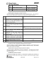
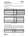
CC2431
CC2431DK
Development Kit
User Manual
Rev. 1.5
SWRU076D
Page 1 of 32
CC2431
Table of contents
1.
2.
3.
4.
5.
5.1
5.2
INTRODUCTION ......................................................................................................................4
ABOUT THIS MANUAL ..........................................................................................................4
DEFINITIONS............................................................................................................................4
CC2431DK CONTENT..............................................................................................................5
SYSTEM OVERVIEW ..............................................................................................................6
GRID..............................................................................................................................................6
NODES ...........................................................................................................................................7
5.2.1
5.2.2
5.2.3
Reference Node ..................................................................................................................................................................... 7
Blind Node............................................................................................................................................................................. 7
Dongle ................................................................................................................................................................................... 7
5.3
5.4
5.5
5.6
6.
6.1
6.2
7.
7.1
7.2
7.3
7.4
8.
8.1
8.2
9.
9.1
9.2
9.3
9.4
10.
10.1
RSSI..............................................................................................................................................7
PROGRAM FLOW ............................................................................................................................8
COMMUNICATION FLOW ...............................................................................................................8
TYPE DEFINITIONS .........................................................................................................................8
IAR EMBEDDED WORKBENCH PROJECT .....................................................................10
CONFIGURATIONS........................................................................................................................10
EMBEDDED SOFTWARE ARCHITECTURE ......................................................................................11
HARDWARE DESCRIPTION ...............................................................................................13
BATTERY BOARD ........................................................................................................................13
PROGRAMMING OF SOC_BB.......................................................................................................14
SMARTRF04EB...........................................................................................................................16
CC2430DB .................................................................................................................................16
NODES ......................................................................................................................................17
SETUP/ START-UP ........................................................................................................................17
LEDS ..........................................................................................................................................17
LOCATION ENGINE WINDOWS GUI................................................................................17
OVERVIEW ..................................................................................................................................17
INSTALLATION.............................................................................................................................18
CONNECTIONS .............................................................................................................................18
INTERACTION WITH OTHER NETWORK NODES ..............................................................................19
GRAPHICAL USER INTERFACE........................................................................................20
MENUS AND BUTTONS .................................................................................................................21
10.1.1
Settings ...................................................................................................................................................................... 21
10.2
SETTINGS PANELS ........................................................................................................................22
10.2.1
10.2.2
10.2.3
10.2.4
Setup.......................................................................................................................................................................... 22
Background ............................................................................................................................................................... 22
Reference Node Setup ............................................................................................................................................... 23
Blind Node Setup....................................................................................................................................................... 24
THE STATUS BAR ........................................................................................................................24
10.3
11.
NODES ......................................................................................................................................25
10.1 BLIND NODE THEORY OF OPERATION .............................................................................................25
11.1.1
11.1.2
11.2
11.3
12.
12.1
12.2
12.3
12.4
12.5
12.6
12.7
12.8
12.9
13.
Polled Mode .............................................................................................................................................................. 25
Auto Mode ................................................................................................................................................................. 26
REFERENCE NODE THEORY OF OPERATION .................................................................................26
LOCATION DONGLE THEORY OF OPERATION ..............................................................................26
MESSAGES ..............................................................................................................................26
XY-RSSI REQUEST (CLUSTER ID: 0X0011)................................................................................26
XY-RSSI RESPONSE (CLUSTER ID: 0X0012) ..............................................................................26
BLIND NODE FIND REQUEST (CLUSTER ID: 0X0013) ..................................................................27
BLIND NODE FIND RESPONSE (CLUSTER ID: 0X0014) ................................................................27
REFERENCE NODE CONFIGURATION (CLUSTER ID: 0X0015)......................................................27
BLIND NODE CONFIGURATION (CLUSTER ID: 0X0016)...............................................................28
REFERENCE NODE CONFIGURATION REQUEST (CLUSTER ID: 0X0017).......................................28
BLIND NODE CONFIGURATION REQUEST (CLUSTER ID: 0X0018) ...............................................28
RSSI BLAST (CLUSTER ID: 0X0019) ...........................................................................................28
CONSTANTS IN SOFTWARE...............................................................................................29
SWRU076D
Page 2 of 32
CC2431
13.1
13.2
14.
15.
TIMING CONSTANTS ....................................................................................................................29
RSSI AVERAGING CONSTANTS ....................................................................................................29
SCHEMATICS .........................................................................................................................30
DOCUMENT HISTORY .........................................................................................................32
SWRU076D
Page 3 of 32
CC2431
1.
Introduction
This CC2431DK User Manual describes how to use the software and hardware included in
the CC2431 Development Kit.
Please refer to the Quick Start Guide for a brief introduction on how to get started using the
development kit.
2.
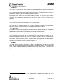
About this manual
This manual contains some of the theoretical material needed to develop a positioning system
based on CC2431 and gives a brief introduction to the software provided in the kit.
3.
Definitions
Blind Node
Reference Node
GUI
Chipcon Packet Sniffer
Z-location Engine
RSSI
TIMAC
SOC_BB
CC243xEM
CC2430-F128
A node using CC2431 and the Location Engine to calculate its
own position.
A node located on a static location.
Graphic User Interface
A PC tool to visualize traffic on radio
A PC tool used to configure and display location engine results
Received Signal Strength Indicator
Texas Instruments Media Access Control, a SW protocol that
handles IEEE 802.15.4 data handling
System on Chip Battery Board
CC2430/ CC2431 Evaluation Module, a small plug-in module
for SmartRF04DK, should be used as reference design for RF
layout.
CC2430 with 128 kB FLASH
SWRU076D
Page 4 of 32
CC2431
4.
CC2431DK content
The development kit contains the following:
2
10
2
10
12
2
1
1
1
x SmartRF04EB
x SOC_BB (Battery Board)
x Evaluation Modules CC2430EM
x Evaluation Modules CC2431EM
x 2.4GHz Antennas
x USB cables
x RS232 Serial cable
x 10-wire flat cable for using SmartRF04EB as emulator for external target systems
x Quick start guide
SmartRF04EB with CC2430EM
Battery board with CC2431EM
The SmartRF04DK Development Kit includes a sample application for location calculation
and demonstration. The sample application allows you to:
•
•
•
Evaluate the SmartRF®04 products. Apply power the boards and the plug and play kit
can be used for range testing and location engine testing
Use SmartRF® Studio to perform RF evaluation and measurements. The radio can be
easily configured to measure sensitivity, output power and other RF parameters.
Develop and test your own firmware. The CC2431DK includes a USB interface that
can be used as an emulator interface for the CC2430 or CC2431. All I/O ports are
available on pin connectors on the edge of the board to allow easy access for testing
or for external I/O.
SWRU076D
Page 5 of 32
CC2431
5.
System overview
For an introduction to the location engine please see application note AN042,
document number SWRA095. The note is available from www.ti.com.
Bl
d
in
de
no
R
ce
en
er
ef
de
no
Figure 1: Location Estimation
The location algorithm used in CC2431 Location Engine is based on RSSI (Received Signal
Strength Indicator) values. The RSSI value will decrease with increasing distance. An
important parameter related to the performance of the location estimate is the absolute
tolerance of the RSSI measurement of the RF-transceiver. This is specific to our transceiver
and is provided in the datasheet. The main feature of the CC2431 Location Engine is that the
location estimation is performed in each Blind Node, hence the algorithm is decentralized.
This reduces the amount of data transferred on the RF interface, since only the calculated
position is transmitted.
The location engine implemented in CC2431 can use up to 16 Reference Nodes for each
calculation. The data that is necessary to do a calculation are X, Y and RSSI values for each
of the Reference Nodes used in the system setup. In addition it needs two RF transmission
parameters (A and N), please refer to application note AN042 for a description of each
parameter.
5.1 Grid
To map each location to a distinct place in the natural environment, a two dimensional grid is
used. The direction will, in the following, be named X and Y. The CC2431 Location Engine
can only handle two dimensions, but it’s possible to handle a third dimension in software (i.e.
to represent levels in a building). The point named (X, Y) = (0, 0) is located in upper left
corner of the grid.
SWRU076D
Page 6 of 32
CC2431
5.2 Nodes
The CC2431 Location Engine uses the RSSI value combined with the physical location of the
Reference Nodes to calculate its own position.
Any number of Reference Nodes can be used in the system, but a node can only calculate its
position if it is within range of at least three Reference Nodes1.
Experiments have shown that one Reference Node for each 100 m2 gives good location
estimates. The nodes should be placed in a grid with one node for each 10 meters in both
directions.
5.2.1
Reference Node
A node which has static location is called a Reference Node. This node must be configured
with an X and a Y value that correspond to the physical location.
The main task for a Reference Node is to provide “reference” packets to the Blind Node.
Reference packets contain the X and Y coordinates of the Reference Node.
5.2.2
Blind Node
A Blind Node will communicate with its nearest Reference Nodes, collecting X, Y and RSSI
values for each of these nodes. Then it uses the location engine hardware to calculate its
position based on the collected parameters from several Reference Nodes.
5.2.3
Dongle
The Dongle will communicate with the entire network; it can request or configure the X,Y
values of all Reference Nodes and the A and N values of the Blind Nodes via the Z-location
Engine PC Application. The Z-location Engine can also configure any Blind Node to
automatically make a periodic position calculation and report (by default the Blind Node is
waiting for a command to perform a position calculation.)
5.3 RSSI
The RSSI value is typically in the range -40 dBm to -90 dBm, where -40 dBm is the highest
value. -40 dBm is approximately the measured signal strength on distance of one meter. Input
to the location engine hardware is the absolute value of the RSSI in dBm, so the range will
typically be from 40 to 90, where 40 is the highest signal strength.
1
Three is a lower theoretical limit, for a good estimate three Reference Nodes may be too
few.
SWRU076D
Page 7 of 32
CC2431
5.4 Program flow
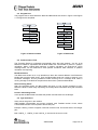
The program flow for both Reference Node and Blind Node are shown in Figure 2 and Figure
3. The figures are simplified.
Figure 2: Reference Node
Figure 3: Blind Node
5.5 Communication Flow
The Z-location Engine is configured to periodically query the entire network – the X,Y of all
Reference Nodes is requested and all Blind Nodes are commanded to perform a position
calculation. When a Blind Node performs a position calculation, the Over-the-Air (OTA)
message traffic can be observed as three phases: broadcast, data collection, & position
calculation and reporting.
Broadcast Phase
The Blind Node sends out a 1-hop broadcast to learn the network address of all Reference
Nodes that are within radio range. Then the Blind Node sends out a blast of several 1-hop
broadcast messages, and any Reference Node receiving such a message shall make a
running average of the RSSI of the packets received from a particular Blind Node.
Data Collecting Phase
After the broadcast phase, the Blind Node will send a 1-hop unicast message to every
Reference Node in radio range requesting the average RSSI calculated during the broadcast
blast.
Position Calculating Phase
In this phase the Blind Node calculates the position and transmits it to the Dongle.
5.6 Type definitions
Some values are given in the notation:
UINTTotalBits_FractionalBits, this means unsigned, total TotalBits number of bits, where
FractionalBits number of bits represent the fraction part.
Example: UINT8_2 means unsigned, 8 bits with 2 fraction bits. This leaves 6 bit to the integer
part.
Both “UINT8_1”, “UINT8_2” and “UINT16_2” are used in the source code.
SWRU076D
Page 8 of 32
CC2431
Notation
UINT8_1
UINT8_2
UINT16_2
Max
127,5
63,75
16 383,75
Accuracy
0.5 meter
0.25 meter
0.25 meter
Table 1: Notation
SWRU076D
Page 9 of 32
CC2431
6.
IAR Embedded Workbench Project
The CC2431DK development kit is delivered with the software preprogrammed into the
CC2431 on the evaluation modules. The location demo can be started right out of the box by
following the instructions in the CC2431DK Quick Start Instructions included in the kit. The
Quick start instructions can also be downloaded from the CC2431 product web site.
The source code is described in this user manual as it gives a good understanding of how the
location demo works.
6.1 Configurations
The remainder of this chapter describes how to set up a location network with 3 or more
Reference Nodes and 1 or more Blind Nodes.
Download the from the CC2431 product page on www.ti.com
• TIMAC (Requires registration)
• Location engine example source code
• Z-location Engine PC application
Install the Z-location Engine and IAR Workbench.
The Location engine example source code is provided as a sample application in the TIMAC.
To install the location sample source code in the right directory copy the zip file with the
source code to C:\Texas Instruments\TI-MAC-1.1.0. Unzip the file and preserve file paths,
this will copy the source files to C:\Texas Instruments\TI-MAC-1.1.0\Projects\mac\Location
Navigate to the IAR_Files project directory located at:
C:\Texas Instruments\TI-MAC-1.1.0\Projects\mac\Location\cc2430\IAR Project
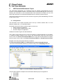
Launch the IAR Embedded Workshop by double clicking on the SampleApp.eww file:
Figure 4: Location Software Project Directory
In the location software workspace there exist three different project configurations:
• CC2430BB
• CC2430DB
• CC2430EB
SWRU076D
Page 10 of 32
CC2431
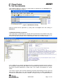
The hardware platform of choice for a build should be selected from the Workspace pulldown menu as displayed in Figure 5.
Figure 5: IAR Workbench Setup
Build the desired device application by pulling down the Project menu and clicking on
Rebuild All
6.2 Embedded Software Architecture
The location logic is implemented as a simple client layer built atop of the TIMAC. Each of the
three different devices must be built individually by removing the comment from the line with
the name of the device desired in the LocationProfile.h. Here is how to build a Dongle:
From a IEEE 802.15.4 network standpoint there is no coordinator and the protocol is setup to
be a proprietary network using the TIMAC as an abstraction layer with the use of the of the
MCPS-SAP primitive MCPS-DATA. Please refer to the TIMAC documentation for further
details.
The Chipcon CC2431 SoC includes hardware functionality implementing the PHY layer and
parts of the TIMAC layer. E.g., the FCS (IEEE 802.15.4 term for CRC) generation and
verification is implemented in CC2431 hardware. The physical layer is not implemented as a
SWRU076D
Page 11 of 32
CC2431
separate layer within the source code, but is merged with the TIMAC sub-layer for
performance and code-size purposes.
SWRU076D
Page 12 of 32
CC2431
7.
Hardware description
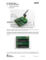
7.1 Battery Board
LED
Button S1
I/O Connector A
SoC Debug
connector
Power Switch
I/O Connector B
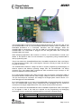
Figure 6: System on Chip Battery Board with CC2430EM
Figure 6 is showing the system on chip battery board. The main function for this board is to
power the CC2430 or CC2431EM with use of two AA batteries.
The System on Chip battery board should be powered by two AA batteries. It can in addition
be powered by a lab power connected directly to GND and VDD on the board. The user
should notice that no voltage converter is used; the lab power voltage is connected directly to
the chip.
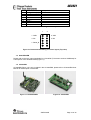
Figure 7: Bottom side of SoC Battery Board
I/O connector A and B gives access to all I/O on the SoC and to some additional pins. I/O
connector A and B have the same pin out as P10 and P11 on the SmartRF04EB. Details can
SWRU076D
Page 13 of 32
CC2431
be found in the schematic in Figure 26 and in the CC1110DK, CC2430DK, CC2510DK
Development Kit User Manual (SWRU039).
The SoC Debug connector can be used both for downloading firmware to the flash and for
debugging of the chip. For both actions use of SmartRF04EB as an In Circuit Emulator is
required.
This board exists in two different versions, PCB version 1.0 and 1.1. The only noticeable
difference between these two versions is the option for disconnection Button S1.
The most important pins on P4 are pin 3-4 for enabling the LED, and pin 5-6 to enable the
button S1. Pin 1 is P1.6 (TD) and pin 2 is P1.7 (RD) for easy access to UART. Pin 7 is VDD
and pin 8 is GND.
CC2430/
EM
connector
P4
I/O Connector
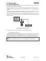
Figure 8: Battery board Signal flow
Power to the board can be switched on and off by using power switch P3.
7.2 Programming of SOC_BB
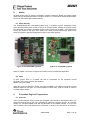
CC2431EM can be programmed / debugged when mounted on SOC_BB. Connect a 10-wire
ribbon cable between P14 on SmartRF04EB and P5 on SOC_BB as shown in Figure 9.
SOC_BB most be powered from batteries and turned on when programming is performed.
NOTE:
The voltage on SOC_BB must be above 2.7 V when debugged from SmartRF04EB.
SWRU076D
Page 14 of 32
CC2431
Figure 9: SmartRF04EB to program SOC_BB
The SmartRF04EB is used as ICE for external target hardware such as the SOC_BB. To use
the SmartRF04EB as ICE, the IAR Embedded Workbench software must be installed. The
Embedded Workbench is a C-Compiler, Simulator, and ICE debugger. When the
SmartRF04EB is connected to a PC with the USB port, the debugger will connect to the
SmartRF04EB. The CC2431EM is plugged into the SOC_BB board when running the
SmartRF04EB in this mode.
When designing applications with CC2430 or CC2431 it is recommended to include a pin
header or test points to allow in-circuit emulation or programming using SmartRF04EB or
other programming tools.
The pin-out used on the SmartRF04EB and the CC2430DB is explained in Table 2 and Figure
10. The connector includes 4 SPI control signals. These are currently not used, but they are
included for flexibility.
The SmartRF04EB includes a voltage converter to support programming and debugging of
external systems with different operating voltage than the SmartRF04EB. The debug
connector (P14, “SoC debug/ flash”) includes two VDD connections on pin 2 and pin 9. The
function is different for these connections.
Pin 2 VDD supplies voltage to the voltage converter. This pin should be connected to VDD on
the external board to assure that the correct supply voltage is used for the voltage converter.
This pin must always be connected. The voltage on the target system must be above 2.7 V
when debugged from SmartRF04EB.
Pin 9 VDD supplies VDD (3.3 V) from the SmartRF04EB. If the target application is powered
from the SmartRF04EB supply during programming and debugging this pin should be
connected. If the target voltage differs from 3.3V, this pin should not be connected.
The pin out used on the SmartRF04EB and the CC2430DB is explained in Table 2 and Figure
10. All signals in bold in the table are required for the programming and debugging
functionality. Figure 10 shows the required signal for a minimum connector layout.
Pin
1
2
Function
GND
VDD
Note
Used to set correct voltage for the
SWRU076D
Page 15 of 32
CC2431
voltage level converter
3
4
5
6
7
8
9
10
Debug Clock (DC)
Debug Data (DD)
CSn
SCLK
Reset_N
MOSI
3.3V VDD, alt. NC
MISO
Delivers VDD from SmartRF04EB
Table 2: P14 SoC debug connector pin-out
1
2
1. GND
2. VDD
3. DC
4. DD
7. Reset_N
Figure 10: Recommended debug connector layout (Top view)
7.3 SmartRF04EB
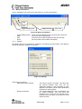
Please refer to the user manual available for CC2430DK (Ti document number SWRU039) for
a description of the SmartRF04EB (Figure 11).
7.4 CC2430DB
CC2430DB (Figure 12) is only included in the CC2430ZDK, please refer to CC2430ZDK User
Manual for a description of the board.
Figure 11: SmartRF04EB
Figure 12: CC2430DB
SWRU076D
Page 16 of 32
CC2431
8.
Nodes
All Blind Nodes must be CC2431 evaluation modules. Reference Nodes and packet sniffer
nodes may be equipped with either CC2430 or CC2431. If a CC2430 is used as a Blind Node,
an LED on the board used will start blinking.
8.1 Setup/ Start-up
The SmartRF04EB and CC2430DB boards have a 5-position joystick, designated U400,
which provides these switch inputs as shown in the table below. Moving the joystick toward
the U400 label (up position) activates the SW1 input. Switch inputs SW2 – SW4 result from
moving the joystick to the right, down (away from U400), and left respectively. SW5 occurs
when the joystick is pressed straight down when in the center position.
Upwards
Upwards
Figure 13: SmartRF04EB, joystick
Figure 14: CC2430DB, joystick
Refer to chapter 9 for how to configure the nodes from the provided PC application.
8.2 LEDs
In each project there is a header file that is customized for the hardware named
hal_board_cfg.h and it contains the following:
#define HAL_LED TRUE
When this symbol is defined to TRUE, the LED’s available on the platform will blink to signal
different states for the node. It is recommended to define HAL_LED to FALSE in order to
increase battery lifetime.
9.
Z-Location Engine PC application
9.1 Overview
The Z-Location Engine communicates with a ZigBee node through a UART/serial cable. The
node connected to the PC will in the following be called the “Location Dongle”. The location
dongle is a complete ZigBee node and will participate in the ZigBee network. It is up to the
user to decide if this node should be a coordinator, a router, or an end device. This node is
SWRU076D
Page 17 of 32
CC2431
used to issue messages into the network, and the other nodes in the network are using the
dongle for addressing packets to the PC application.
Figure 15: Overview
It’s recommended to use a SmartRF04EB for the location dongle, since this board gives easy
access to a UART connection. The dongle node can use either a CC2430 or a CC2431 RF
chip
The Z-Location Engine includes a flash download function, which makes it possible to
download an already generated hex file to a connected development board. Please note that
flash programming can only be done with use of a USB cable. How to perform flash
programming is described later in this manual.
9.2 Installation
The Z-Location Engine is distributed as an executable installation file. This file can be
downloaded from the CC2431 product page on www.ti.com. The installation file will add an
item to the start menu. The Z-Location Engine application can be started by clicking [Start] ->
[Programs] -> [Chipcon] – [Z-Location Engine].
9.3 Connections
Figure 16: Connections, USB is optional
The SmartRF04EB should be powered either from a power supply or from USB. The PC must
be connected to the SmartRF04EB using a UART cable2. All communication when the system
is operating is over the UART. If a USB cable is connected, this makes it possible to
download firmware directly from the Z-Location Engine PC application. The USB can in
addition be used for downloading and debugging the dongle node from e.g. the IAR
embedded workbench development environment.
2
A UART cable is often called RS-232 cable, serial cable, or null-modem cable. It connects to
a serial port on the PC and to the D-SUB connector (P200) on the SmartRF04EB.
SWRU076D
Page 18 of 32
CC2431
9.4 Interaction with other network nodes
The PC application will from time to time issue two different broadcast messages into the
network. This is done through the location dongle, which is a complete node that participates
in the network. All nodes associated to the network will show up as either reference nodes or
blind nodes in the Z-Location Engine PC application.
Below is a highly simplified version of the algorithm used.
Broadcast request for blind nodes
Wait for broadcast reply
Broadcast request for reference nodes
Wait for broadcast reply
Iterate the list of received blind nodes
Unicast request for calculated position
Wait for reply
Repeat from start
Some of the timer intervals in the algorithm can be changed by the user. Please notice that
the actual implementation is not sequential, even if the pseudo code looks that way.
SWRU076D
Page 19 of 32
CC2431
10. Graphical User Interface
Interaction with the Z-Location Engine is done through graphical user interface shown below.
The user interface and menus are described in the following sections.
Figure 17: Z-Location Screenshot
SWRU076D
Page 20 of 32
CC2431
10.1 Menus and buttons
The PC application has a few menus and buttons to control the application.
Stop
Start
Toggle settings panel
Slider for zoom
Zoom level
Figure 18: Menus and buttons
-
Toggle settings panel:
Start:
Stop:
Zoom:
Show / hide the settings panel in the lower part of the GUI
Connect to the location dongle
Disconnect the location dongle and clear all node lists
Set zoom level of the location area display
10.1.1 Settings
All settings that can be changed are available in the dialog box shown below. This dialog is
opened by pressing “Settings” in the menu.
Figure 19: Settings
Node discovery interval:
- Start Node request interval:
-
Remove node after:
This value is given in seconds. The value sets
the interval between each time the PC
application attempt to start broadcast of node
requests. The value 0 can be used to disable the
broadcast of node requests.
The nodes registered by the PC application will
be checked regularly. The time since last
message from a node will be checked and if
longer than the time given in this field, the node
will be removed.
SWRU076D
Page 21 of 32
CC2431
-
-
Request Conf. data Ref. Nodes:
Checkbox to control the broadcast of “Request
of configuration data from ref. nodes.” If not
checked, the message will not be sent to the ref.
nodes.
Request Conf. data Blind Nodes:
Same as above but for the Blind nodes.
Request Position data blind nodes: Checkbox to control the Request of position data
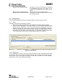
from the blind nodes.
10.2 Settings panels
The Z-Location Engine implements four settings panels in the lower part of the GUI.
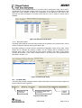
10.2.1 Setup
The setup panel serves the following purposes:
1. Select which COM port that is used. The application supports COM1 to COM20.
2. Give the user the possibility to download firmware to a connected development board
directly from the application. This can be done easily by selecting the hex file to
program, selecting the correct device from the device list and pressing “Load FW”.
Note that this flash programming utility always will retain the IEEE address stored in
the 8 last bytes in the flash of CC2430/CC2431. To generate a HEX file, please refer
to the Texas Instruments IAR user manual available from the TI web site.
Figure 20: Setup Panel
10.2.2 Background
The PC application can show a map as a background image on the area where all the nodes
are displayed. The map must be an image of file type bmp. To add a map, select the file you
want to use, type in the width and height for this map in meters, and click “Update”.
Remember to check “Show background image”.
SWRU076D
Page 22 of 32
CC2431
Figure 21: Background Panel
By checking or unchecking “Visible grid” and / or “Show background image” different views
can be selected. Figure 22 shows the effect of these check boxes. The upper left figure in the
shows both boxes unchecked, the next image shows “Visible grid” checked, the next shows
both checked and the lowermost right image shows “Visible grid” unchecked and “Show
background image” checked.
Figure 22: Different background settings
10.2.3 Reference Node Setup
This tab gives the possibility to set up or change X and Y coordinates assigned to each of the
reference nodes. To configure this, double click on a reference node in the list and right click
SWRU076D
Page 23 of 32
CC2431
while pointing to its intended location in the blue area or background map. The X and Y
coordinates of the intended location will be set in the X and Y fields of the Reference Node
Setup tab. Press “Update” to assign the coordinates of the reference node. After a few
seconds the node will appear as a yellow circle and the X and Y values in the list will be
updated.
Figure 23: Reference Node Setup
10.2.4 Blind Node Setup
The Blind node setup tab shows all blind nodes that are present in the system and it can be
used to change the settings used for each blind node.
By double clicking on a node in the list, the present configuration values can be seen. These
values can be changed. By pressing “Update” the new settings will be transferred to the
selected node. After a few seconds the node will be updated. The status of this update
process will be shown in the column named “Status” in the device list. The parameters are
described in chapter 12.6
Figure 24: Blind Node Setup
10.3 The Status Bar
The status bar provides / displays real time status information for both the location dongle and
the Z-Location Engine in general.
Number of
messages
Number of blind node
messages
Dongle
status
Figure 25: Status Bar
SWRU076D
Page 24 of 32
CC2431
Number of messages:
Shows the total number of incoming messages to the PC
application since the Z-Location Engine was started.
Number of blind node messages:
Shows the total number of incoming blind node
messages since the Z-Location Engine was started. The
Number of unsuccessful messages is the number of
messages that is reported to be false.
Dongle status: Shows the current status for the connected location dongle.
11.
Nodes
10.1 Blind Node Theory of Operation
The Blind Node is the device that contains the CC2431 location engine. The location engine
estimates its position by using the coordinates of all responding reference nodes within direct
radio range (up to 16) along with the average RSSI of messages sent to them. Reference
Nodes are neighbour devices that are within radio range of the Blind Node. The Blind Node
begins a find by broadcasting a sequence of blast message (Cluster ID: 0x0019) with radius
one. After waiting the interval specified in its configuration, the blind node then broadcasts to
the Reference Nodes a position request (Cluster ID: 0x0011), also with radius one in order to
limit the recipients (and thus responders) to the reference nodes in direct radio range.
Each Reference Node that hears the blast broadcasts will begin averaging the RSSI of the
series of messages received. Upon receiving the position request, the Reference Node will
send back to the Blind Node its position information along with the average received signal
strength over the series of blasts.
There are two main modes of operation for the Blind Node in the sample Location Profile.
11.1.1 Polled Mode
This mode requires that the Dongle make a request for the position of the blind node on
demand, and thus the Blind Node will only acquire the Reference Node data when it is
requested using the Blind Node Request command (Cluster ID: 0x0013). It will then
perform the required calculation, and then send a Blind Node Response (Cluster ID:
0x0014) back to the original requester.
When the Blind Node Request command is sent to a Blind Node, the request is processed
in the BlindNode_ProcessEvent() event handler (which handles all the system and user
events for the Blind Node location application). The application is notified of an incoming
over-the-air message from the TIMAC and it processes the incoming message. If the
incoming message has a Cluster ID that matches the Blind Node Request command, then
it will start the process of acquiring the Reference Node information by calling startBlast().
The first thing the BLINDNODE_FIND_EVT event handler does is to turn on the
RxOnWhenIdle flag in the TIMAC capabilities flag of the device. In the case where a Blind
Node is an end device, this is done in order for it to receive Reference Node information
without having to poll for the actual data packet (using a Data Request packet). This also
ensures that end devices can stay awake for the entire period of time when the acquisition
of Reference Node information is taking place.
The Blind Node will then send out a series of 1-hop broadcast messages. Once the Blind
Node finishes blasting it requests the Reference Node audience to send the average RSSI
of messages just sent and waits the configured time for reference nodes to respond.
Finally, it calls the function FinishCollection() to set the RxOnWhenIdle flag to false so
that “normal” end device operation is once again adhered to.
The function sendRsp() is then called to process the received Reference Node data and
calculate the Blind Node’s position based on that information. If the Blind Node was able to
collect data from at least config.minRefNodes number of nodes, the status
BLINDNODE_RSP_STATUS_SUCCESS will be returned as part of the message. If not,
the status BLINDNODE_RSP_STATUS_NOT_ENOUGH_REFNODES will be returned as
part of the message. The response is sent to the device that was the originator of the Blind
Node Request.
SWRU076D
Page 25 of 32
CC2431
The entire process is started again when another Blind Node Request is received.
11.1.2 Auto Mode(Default)
In Auto Mode, the process for acquiring the Reference Node data is exactly the same as
for polled mode, except this mode allows the Blind Node to start collecting Reference
Node data automatically in a periodic fashion by timer or user event (such as a button
press) without having to be manually asked by the host-system. By default, the Blind
Node Response is then sent to the Dongle (short address 0x0000). However, the user can
also configure the destination address.
The user can also set or request the configuration parameters for the Reference Nodes
and Blind Nodes by using the following Cluster IDs:Reference Node Configuration (Cluster
ID: 0x0015)Blind Node Configuration (Cluster ID: 0x0016)Reference Node Configuration
Request (Cluster ID: 0x0017)Blind Node Configuration Request (Cluster ID: 0x0018)
11.2 Reference Node Theory of Operation
When the Reference Node receives a Reference Node Request, it invokes the function sends
the Reference Node coordinate data (along with the received signal strength) directly to the
requester.
11.3 Location Dongle Theory of Operation
The location dongle is an application that uses the serial port to send and receive Location
Profile messages with the Windows GUI. This is typically the device that is attached to the
host-system (e.g. a PC running the Z-Location Engine) and is used as the sink node for
receiving Blind Node Responses and for configuring Reference Node and Blind Node setup
parameters. The connection to the PC is via a serial port, and therefore a device built as a
Dongle must have a serial port. Currently the only 2430 boards with a readily usable serial
port are the EB boards. Therefore, the Sample Application for Dongle will only build as an EB
device. Note that although the Dongle will build as an EndDevice, such a configuration is not
recommended nor tested.
When the location dongle application receives a Blind Node Response message, it will pass
the data to the host-system via the serial port.
12.
Messages
The location protocol messages are defined as follows. All multi-byte fields are transmitted
low byte first. The message is sent as TIMAC payload data with the following format:
Destination Endpoint
1 byte
Cluster Id
2 bytes
Source Endpoint
1 byte
Message Data
N bytes
The possible endpoints, as well as all other constants related to the location protocol are
defined in LocationProfile.h
12.1 XY-RSSI Request (Cluster ID: 0x0011)
Send this to trigger an XY-RSSI Response message. This message should be sent
shortly/immediately after sending a burst of RSSI Blast messages in order to retrieve the
coordinates and average RSSI radio link strength with Reference Nodes that are within 1-hop
radio range. Note that if this message is sent with a radius greater than 1, then the RSSI is
not applicable - only the XY content would be useful. This message doesn’t have a body to
the message.
12.2 XY-RSSI Response (Cluster ID: 0x0012)
This message is sent in response to the XY-RSSI request message. The RSSI average value
includes the RSSI of the RSSI Request message itself, and then the RSSI average is zeroed
SWRU076D
Page 26 of 32
CC2431
in preparation for another series of blasts. Thus, if a blast was never sent, the RSSI average
is just the RSSI value of the request message.
Byte
Index
Description
0&1
Reference Node’s X position
2&3
Reference Node’s Y position
4
Value
Bits 15-2 – whole meters
Bits 1-0 – 0.25 meters
If this field contains 0xFFFF,
the Reference Node hasn’t
been configured
Bits 15-2 – whole meters
Bits 1-0 – 0.25 meters
If this field contains 0xFFFF,
the Reference Node hasn’t
been configured
0 – 255
RSSI Average of any RSSI Blast
broadcasts and that of the request
message itself.
12.3 Blind Node Find Request (Cluster ID: 0x0013)
Send this message to a Blind Node to force it to perform a location find (if a Blind Node is
properly configured to perform finds as often as necessary for its intended use, then the XYRSSI Request should suffice). The response to this message will be sent by the Blind Node
when the location find process is complete, which could take seconds, depending on the total
network traffic. This message doesn’t have a body to the message, but just a cluster ID.
12.4 Blind Node Find Response (Cluster ID: 0x0014)
This message is sent out of the Blind Node in response to the “Blind Node Request”
message.
Byte
Index
0
Description
Value
Status
1&2
Blind Node’s calculated X position
3&4
Blind Node’s calculated Y position
5
6&7
8&9
10 & 11
12
Number of Reference Nodes used in
calculation
Closest (based on RSSI) Reference
Node’s short address
Closest Reference Node’s X position
Closest Reference Node’s Y position
0 – Success
1 – Not enough Reference
Node responding
Bits 15-2 – whole meters
Bits 1-0 – 0.25 meters
Bits 15-2 – whole meters
Bits 1-0 – 0.25 meters
0–8
0x0000 – 0xFFFA, 0xFFFE is
invalid
Bits 15-2 – whole meters
Bits 1-0 – 0.25 meters
Bits 15-2 – whole meters
Bits 1-0 – 0.25 meters
Closest Reference Node’s RSSI
12.5 Reference Node Configuration (Cluster ID: 0x0015)
Send this message to the Reference Node to set its configuration items. This message is
also sent from the Reference Node in response to the “Reference Node Configuration
Request”.
SWRU076D
Page 27 of 32
CC2431
Byte
Index
Description
Value
0&1
Reference Node’s X position
2&3
Reference Node’s Y position
Bits 15-2 – whole meters
Bits 1-0 – 0.25 meters
Bits 15-2 – whole meters
Bits 1-0 – 0.25 meters
12.6 Blind Node Configuration (Cluster ID: 0x0016)
Send this message to the Reference Node to set its configuration items. This message is
also sent from the Blind Node in response to the “Blind Node Configuration Request”.
Byte
Index
0
1
2
3&4
5&6
7&8
9
10
Description
Value
Blind Node’s A parameter. “A” is defined as the
absolute value of the average power in dBm
received at a close-in reference distance of one
meter from the transmitter, assuming an omnidirectional radiation pattern.
Blind Node’s N parameter, which is the path loss
index that describes the rate at which the signal
power decays with increasing distance from the
transmitter.
Operating Mode
Collect Time – the number of milliseconds to
wait for Reference Node Responses after
sending the request.
Cycle Time – Low byte first. The number of
milliseconds to wait before starting the
calculation cycle.
Only valid in the Auto
Operating Mode.
Report Short Address – low byte first.
Destination address for Blind Node Response
messages in AUTO mode. In POLL mode, the
response is returned to the requestor’s address.
Report Endpoint – Destination endpoint for Blind
Node Response message in AUTO mode.
Minimum Reference Nodes to use to calculate
location.
0 – Polled. Waits for Blind Node Requests to do a find
& rsp
1 – Automatically initiate a location find and response.
In 100 millisecond increments
In 100 millisecond increments
0x0000 – 0xFFFF
1 – 16
12.7 Reference Node Configuration Request (Cluster ID: 0x0017)
Send this message to a Reference Node to request its configuration. The response to this
request is the Reference Node Configuration message (Cluster ID 0x0015). This message
doesn’t have a body to the message.
12.8 Blind Node Configuration Request (Cluster ID: 0x0018)
Send this message to a Blind Node to request its configuration. The response to this request
is the Blind Node Configuration message (Cluster ID 0x0016). This message doesn’t have a
body to the message.
12.9 RSSI Blast (Cluster ID: 0x0019)
Broadcast this message with a radius of 1, several times in relatively short succession to
trigger Reference Nodes within radio range to average the RSSI (received signal strength
SWRU076D
Page 28 of 32
CC2431
indication) of the blast of broadcasts received. This message doesn’t have a body to the
message.
13.
Constants in software
This chapter describes some of the constants used in the software. These constants can be
modified to change the behavior of the location system. The constants are all defined in the
file blindnode.c.
13.1 Timing constants
All values related to timing are defined with macros.
Constant
Default
value
100
20
BN_TIME_INCR
BLINDNODE_FIND_DELAY
BLINDNODE_WAIT_TIMEOUT
2
BLINDNODE_BLAST_DELAY
20
Description
Milliseconds per time increment.
Delay between automatic location
find calculations in BN_TIME_INCR
ticks.
Delay between blasting and polling
the Reference Nodes and between
each poll in BN_TIME_INCR ticks.
Milliseconds to delay in between
each blast.
Table 3: Timing constants
Constant
BLINDNODE_MAX_REF_NODES
Default
value
20
BLINDNODE_MIN_REF_NODES
3
BLINDNODE_BLAST_COUNT
8
Description
Maximum number of Reference
Nodes to poll for the RSSI average
before selecting the best 16 and
feeding them to the location
engine.
Minimum number of Reference
Nodes to feed to the location
engine.
Number of 1-hop broadcasts to
blast.
Table 4: Other Constants
13.2 RSSI averaging constants
The RSSI value used as input to the location engine hardware should be as accurate as
possible. Averaging of the RSSI value is used to improve the accuracy. The Blind Node blasts
a number of 1-hop broadcasts to the Reference Nodes which calculate the running average
RSSI of the received blasts. The default number of blasts to send for the averaging is shown
in the table below. It is recommended to average over 2, 4, 8 or 16 packets to avoid time
demanding division in the microcontroller. The actual value to use is a trade of between
position accuracy and update frequency / power consumption.
Constant
BLINDNODE_BLAST_COUNT
Default
value
8
Description
Number of 1-hop broadcasts to blast for
the Reference Nodes to calculate the
average.
Table 5: Number of values used in averaging
SWRU076D
Page 29 of 32
CC2431
13.3 Radio channel settings and PANID
By default the location example applications are configured to used channel 16 (0x10) and
using PANID 0x11CC. The channel and PANID can be changed in msa.h
14.
Schematics
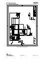
The schematic for the SOC_BB (Battery Board) is shown below.
The CC2431EM is equal to the CC2430EM except for the CC2430/CC2431 chip. The
complete reference design for the CC2430EM can be downloaded from the CC2430 product
web site.
Schematic for the SmartRF04EB is found in the CC1110DK, CC2430DK, CC2510DK
Development Kit User Manual (SWRU039).
SWRU076D
Page 30 of 32
CC2431
Figure 26: SOC_BB Schematics
SWRU076D
Page 31 of 32
CC2431
15.
Document history
Revision
1.0
1.1
1.2
Date
2006-03-10
2006-06-01
2006-08-14
1.3
1.4
1.5
2006-11-14
2007-03-13
2007_06_05
Description/Changes
Initial release.
Minor changes
Some changed in the structure of the manual. Updated to reflect
some changes in the IAR project files.
Minor changes to make the document easier to read.
Updated with new PC GUI and TIMAC
Changed constant values to correspond with MAC 1.1.0 release
SWRU076D
Page 32 of 32
IMPORTANT NOTICE
Texas Instruments Incorporated and its subsidiaries (TI) reserve the right to make corrections, modifications, enhancements,
improvements, and other changes to its products and services at any time and to discontinue any product or service without notice.
Customers should obtain the latest relevant information before placing orders and should verify that such information is current and
complete. All products are sold subject to TI’s terms and conditions of sale supplied at the time of order acknowledgment.
TI warrants performance of its hardware products to the specifications applicable at the time of sale in accordance with TI’s
standard warranty. Testing and other quality control techniques are used to the extent TI deems necessary to support this
warranty. Except where mandated by government requirements, testing of all parameters of each product is not necessarily
performed.
TI assumes no liability for applications assistance or customer product design. Customers are responsible for their products and
applications using TI components. To minimize the risks associated with customer products and applications, customers should
provide adequate design and operating safeguards.
TI does not warrant or represent that any license, either express or implied, is granted under any TI patent right, copyright, mask
work right, or other TI intellectual property right relating to any combination, machine, or process in which TI products or services
are used. Information published by TI regarding third-party products or services does not constitute a license from TI to use such
products or services or a warranty or endorsement thereof. Use of such information may require a license from a third party under
the patents or other intellectual property of the third party, or a license from TI under the patents or other intellectual property of TI.
Reproduction of TI information in TI data books or data sheets is permissible only if reproduction is without alteration and is
accompanied by all associated warranties, conditions, limitations, and notices. Reproduction of this information with alteration is an
unfair and deceptive business practice. TI is not responsible or liable for such altered documentation. Information of third parties
may be subject to additional restrictions.
Resale of TI products or services with statements different from or beyond the parameters stated by TI for that product or service
voids all express and any implied warranties for the associated TI product or service and is an unfair and deceptive business
practice. TI is not responsible or liable for any such statements.
TI products are not authorized for use in safety-critical applications (such as life support) where a failure of the TI product would
reasonably be expected to cause severe personal injury or death, unless officers of the parties have executed an agreement
specifically governing such use. Buyers represent that they have all necessary expertise in the safety and regulatory ramifications
of their applications, and acknowledge and agree that they are solely responsible for all legal, regulatory and safety-related
requirements concerning their products and any use of TI products in such safety-critical applications, notwithstanding any
applications-related information or support that may be provided by TI. Further, Buyers must fully indemnify TI and its
representatives against any damages arising out of the use of TI products in such safety-critical applications.
TI products are neither designed nor intended for use in military/aerospace applications or environments unless the TI products are
specifically designated by TI as military-grade or "enhanced plastic." Only products designated by TI as military-grade meet military
specifications. Buyers acknowledge and agree that any such use of TI products which TI has not designated as military-grade is
solely at the Buyer's risk, and that they are solely responsible for compliance with all legal and regulatory requirements in
connection with such use.
TI products are neither designed nor intended for use in automotive applications or environments unless the specific TI products
are designated by TI as compliant with ISO/TS 16949 requirements. Buyers acknowledge and agree that, if they use any
non-designated products in automotive applications, TI will not be responsible for any failure to meet such requirements.
Following are URLs where you can obtain information on other Texas Instruments products and application solutions:
Products
Applications
Amplifiers
amplifier.ti.com
Audio
www.ti.com/audio
Data Converters
dataconverter.ti.com
Automotive
www.ti.com/automotive
DSP
dsp.ti.com
Broadband
www.ti.com/broadband
Interface
interface.ti.com
Digital Control
www.ti.com/digitalcontrol
Logic
logic.ti.com
Military
www.ti.com/military
Power Mgmt
power.ti.com
Optical Networking
www.ti.com/opticalnetwork
Microcontrollers
microcontroller.ti.com
Security
www.ti.com/security
RFID
www.ti-rfid.com
Telephony
www.ti.com/telephony
Low Power
Wireless
www.ti.com/lpw
Video & Imaging
www.ti.com/video
Wireless
www.ti.com/wireless
Mailing Address: Texas Instruments, Post Office Box 655303, Dallas, Texas 75265
Copyright © 2007, Texas Instruments Incorporated