1
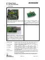
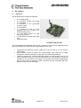
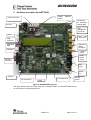
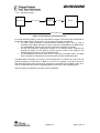
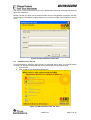
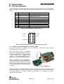
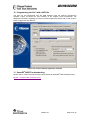
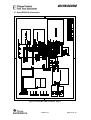
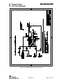
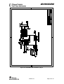
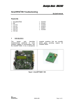
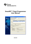
CC1110/CC2510
CC1110DK
CC2510DK
Development Kit
User Manual
Rev. 1.0
SWRU134
Page 1 of 33
CC1110/CC2510
Table of contents
1
2
3
4
4.1
5
5.1
INTRODUCTION ......................................................................................................................3
ABOUT THIS MANUAL ..........................................................................................................3
DEFINITIONS............................................................................................................................4
KIT CONTENT ..........................................................................................................................6
HARDWARE ...................................................................................................................................6
SMARTRF®04EB .......................................................................................................................7
USB MCU ....................................................................................................................................8
5.1.1
5.1.2
Bootloader............................................................................................................................................................................. 8
Programming USB controller............................................................................................................................................... 8
USB MCU SIGNAL NAMES ............................................................................................................9
5.2
6
6.1
6.2
6.3
6.4
6.5
6.6
6.7
6.8
6.9
6.10
7
7.1
7.2
7.3
HARDWARE DESCRIPTION SMARTRF®04EB................................................................10
POWERING SMARTRF®04EB.......................................................................................................11
USB INTERFACE ..........................................................................................................................12
RS-232 INTERFACE......................................................................................................................12
USER INTERFACE .........................................................................................................................12
AUDIO INTERFACE .......................................................................................................................12
SPI INTERFACE SWAP JUMPERS ON SMARTRF®04EB ..................................................................13
I/O CONNECTORS .........................................................................................................................14
EM CONNECTORS ........................................................................................................................15
SIGNAL FLOW ..............................................................................................................................15
EM LCD CONNECTION ................................................................................................................16
APPLICATION EXAMPLES AND RF TESTING...............................................................17
SETUP ..........................................................................................................................................17
EXAMPLES ...................................................................................................................................17
RF TESTING .................................................................................................................................18
7.3.1
7.3.2
Output power testing........................................................................................................................................................... 18
Sensitivity testing................................................................................................................................................................. 19
8
8.1
8.2
8.3
8.4
8.5
9
9.1
9.2
9.3
10
11
12
13
14
IAR EMBEDDED WORKBENCH.........................................................................................20
DOWNLOAD THE LATEST IAR SOFTWARE....................................................................................20
INSTALLATION OF DOWNLOADED EVALUATION VERSION FROM WEB ..........................................20
INSTALLATION FROM THE CD .....................................................................................................21
OBTAINING 60 DAYS ADDITIONAL LICENSE .................................................................................22
IAR EMBEDDED WORKBENCH – KICKSTART EDITION ................................................................22
USING SMARTRF®04EB FOR PROTOTYPING................................................................23
USING SMARTRF®04EB AS AN IN-CIRCUIT EMULATOR (ICE)....................................................23
DEBUG INTERFACE ......................................................................................................................23
SYSTEM-ON-CHIP DEBUG PLUG-IN BOARD (SOC_DEM) ...........................................................24
PROGRAMMING THE SOC WITH A HEX FILE .............................................................25
SMARTRF®04EB TROUBLESHOOTING ...........................................................................25
SMARTRF04DK SCHEMATICS...........................................................................................26
EVALUATION MODULES ....................................................................................................33
DOCUMENT HISTORY .........................................................................................................33
SWRU134
Page 2 of 33
CC1110/CC2510
1
Introduction
Thank you for purchasing a SmartRF®04DK Development Kit.
Please note that Texas Instruments uses the term SmartRF®04DK as a collective term for all
development kits on the Chipcon SmartRF®04 platform. This development platform supports
evaluation, development and prototyping using the Chipcon SmartRF®04 products from
Texas Instruments.
Make sure to subscribe to the Low-Power RF eNewsletter to receive information about
updates to documentation, new product releases and more. Sign up on the Texas
Instruments RF/IF Components web site.
2
About this manual
This manual contains both tutorial and reference information, and covers both the hardware
and software components of the development kit. This manual does not cover the CC2511
USB dongle included in the CC2510-CC2511DK.
The RF USB dongle HW and application examples are covered in a separate document.
SmartRF® Studio has its own user manual.
The Chipcon Flash Programmer has its own user manual.
Further background information can be found in the device datasheets.
SWRU134
Page 3 of 33
CC1110/CC2510
3
Definitions
SmartRF04EB
CC1110EM or CC2510EM
Evaluation Board. Main board with LCD, USB
interface, LEDs, pot-meter etc. Platform for the
Evaluation Modules (EM).
CC1110/CC2510 Evaluation Module, a
small
plug-in
module
for
CC1110DK/CC2510-CC2511DK, should be
used as reference design for antenna and
RF layout.
RF USB Dongle
Reference design for a CC2511 based USB
dongle with RF interface. Should be used as
reference design for antenna and RF layout. HW
and SW application examples for this USB
Dongle is not covered in this document. A
separate RF USB Dongle User Manual covers
this.
SmartRF®04EB
SmartRF®04DK
CC2510EM
CC1110EM
USB MCU
Factory firmware
PER
Evaluation Board. Main board with LCD, USB interface, LEDs, potmeter etc. Platform for the Evaluation Modules (EM, see below).
A collective term used for all development kits for the SmartRF®04
platform, i.e. SmartRF®04EB + EM.
CC2510 Evaluation Module, a small plug-in module for
SmartRF04DK, should be used as reference design for RF layout.
CC1110 Evaluation Module, a small plug-in module for
SmartRF04DK, should be used as reference design for RF layout.
The Silicon Labs C8051F320 MCU used to provide a USB interface
on the SmartRF04DK.
The firmware that is supplied programmed into the USB MCU from
the factory. This firmware supports SmartRF® Studio operation as well
as a stand-alone PER tester.
Packet Error Rate. Counts the number of lost and/or faulty packets
and displays the ratio: (lost/faulty packets)/number of packets sent.
SWRU134
Page 4 of 33
CC1110/CC2510
SoC
ICE
System on a Chip. A collective term used to refer to Texas
Instruments ICs with on-chip MCU and RF transceiver. Used in this
document to reference the CC1110 / CC2510.
In Circuit Emulator.
SWRU134
Page 5 of 33
CC1110/CC2510
4
Kit content
4.1
Hardware
The development kit contains the following:
•
•
•
•
•
•
•
•
2 x SmartRF®04EB
2 x evaluation module (CC1110EM
or CC2510EM)
2 x Antenna for the appropriate
frequency range
2 x USB cables
1 x 10-wire flat cable for using
SmartRF®04EB as emulator for
external target systems
2 x SOC_DEM System on Chip
debug plug-in board
1 x USB dongle (CC2510-CC2511DK
only)
Quick start guide
SmartRF®04EB with EM
The SmartRF04DK Development Kit includes a number of functions and applications that
allows quick testing of the RF interface and peripherals of the chip.
•
•
•
Evaluate the SmartRF®04 products. Right out of the box, the kit can be used for
range testing.
Use SmartRF® Studio to perform RF measurements. The radio can be easily
configured to measure sensitivity, output power and other RF parameters.
Prototype development. The SmartRF04DK includes a USB interface that can be
used as emulator interface for the CC1110/CC2510. All CC1110/2510 I/O ports are
available on pin connectors on the edge of the board to allow external applications
easy access to the CC1110/2510. These connectors are also compatible with logic
analyser probes for easy debugging.
SWRU134
Page 6 of 33
CC1110/CC2510
5
SmartRF®04EB
This chapter includes overall information that applies to SmartRF®04EB. In the following SoC
means Chipcon System on Chip, i.e. CC1110 or CC2510.
Figure 1: Main components
Figure 1 shows the main components on the SmartRF®04EB. A USB cable from a PC is
connected directly to the USB controller. When a SoC evaluation module is plugged into the
SmartRF®04EB, the only purpose of the USB controller is to “translate” USB signals to the
SoC 2-wire debug interface. This interface includes Debug Clock (DC) and Debug Data (DD).
The USB controller also controls the Reset_n line connected to the SoC.
Most of the peripherals on the SmartRF®04EB are connected to both the USB controller and
to the SoC. This means that I/O ports on both controllers can drive the same pin. When the
USB controller detects that a SoC is connected, it will therefore set all the I/O in three-state
(high impedance) mode. The connection to the USB controller may anyhow somewhat
influence these I/O lines.
SWRU134
Page 7 of 33
CC1110/CC2510
5.1
5.1.1
USB MCU
Bootloader
The USB controller is programmed with a bootloader when it is shipped from the factory. The
bootloader allows programming of new code into the USB MCU without the Silicon Labs’
serial adapter. The bootloader communicates with SmartRF® Studio or a custom program via
USB.
5.1.2
Programming USB controller
If it is required to update the firmware of the USB MCU, this can be done using the
SmartRF®04 programming software (Chipcon Flash Programmer or SmartRF® Studio). For
use of Chipcon Flash Programmer please refer to Chipcon Flash Programmer user manual
for instructions. The USB controller can only be updated via USB when no EM is connected to
the SmartRF®04EB.
To download firmware to the USB MCU without using the bootloader or to download the
bootloader in the first place, a Silicon Labs’ EC2 serial adapter (Figure 2) is required. This
adapter should be connected to P301, marked “USB MCU debug”, on the SmartRF®04EB.
Figure 2: EC2 serial adapter
SWRU134
Page 8 of 33
CC1110/CC2510
5.2
USB MCU signal names
The USB MCU is a C8051F320 from Silicon Labs. Please see the Silicon Labs web site for
detailed information about this MCU.
The following table shows the usage of I/O pins on the USB MCU.
Pin
no.
1
Pin name
(USB MCU)
P0.1
Signal name
SmartRF®04EB
P1.7/SO/GDO1/MISO
0-ohm
resistor
R117
2
10
11
12
13
14
15
P0.0
P3.0/C2D
P2.7
P2.6
P2.5
P2.4
P2.3
P1.5/SCLK
R115
P1.3/LED3
P0.4/RTS
RS232_POWER
P2.0/LED_4
RESET_N
R113
R100
16
P2.2
SOC_PRESENT
17
P2.1
P0.6/JOY
R106
18
19
20
21
22
23
24
25
26
27
P2.0
P1.7
P1.6
P1.5
P1.4
P1.3
P1.2
P1.1
P1.0
P0.7
P1.2/LED2
P1.0/LED1
P0.7/POT
P0.5/JOY_PUSH
P1.1/PWM_OUTPUT
P0.1/BUTTON_PUSH
P0.0/MIC_INPUT
P2.4/SCL
P2.3/SDA
P2.2/GDO2/DC
R111
R110
R107
R112
R105
R101
R104
R124
R123
R122
28
P0.6/CNVSTR
P2.1/GDO1/DD
R121
29
30
31
32
P0.5
P0.4
P0.3/XTAL2
P0.2/XTAL1
P0.2/UART_RD
P0.3/UART_TD
P1.4/CSn/SS
P1.6/MOSI
R102
R103
R114
R116
R120
Function
SPI MISO signal,
transceiver/transmitter SO/GDO2
SPI Serial clock
USB MCU Debug pin
LED3 (yellow), active low
Turns RS-232 level converter on/off
LED4 (Blue), active low
LCD Power on reset signal, SoC
RESET
Tells USB MCU whether a SoC is
present.
0 = transmitter/transceiver
1 = SoC
Joystick input (analogue coded
voltage)
LED2 (Red), active low
LED1, (Green), active low
Potentiometer input
Joystick pushed
PWM audio output
Button pushed
Audio input
I2S clock (for LCD)
I2S data (for LCD)
Transceiver/transmitter GDO3, SoC
debug signal
Transceiver/transmitter GDO1, SoC
debug signal
UART RD
UART TD
SPI slave select signal
SPI MOSI signal,
Transceiver/Transmitter SI
Table 1: USB MCU pin-out
As mentioned in the table, the joystick output is coded as an analogue voltage. This has been
done in order to save the number of pins required on the MCU to interface with the joystick.
The SoC software libraries contain functions to decode the ADC values and indicate in what
direction the joystick is moved. The push function of the joystick is treated as a separate
digital signal.
SWRU134
Page 9 of 33
CC1110/CC2510
6
Hardware description SmartRF®04EB
Supply
switch
Power connector
selection
Connectors
for evaluation
module (EM)
DC jack
SoC
debug/flash
connector
LCD
SMA test
connectors
USB
connector
USB MCU
reset
USB MCU
debug
connector
USB MCU
Potentio
meter
Headphone
output
RS-232
connector
Mic.
input
Button
S1
Joystick
I/O connector A
I/O connector B
LEDs
Volume
control
Figure 3: SmartRF04DK overview
The figure above shows the major parts of the SmartRF®04EB. The SmartRF®04EB serves
as main platform in the development kit.
SWRU134
Page 10 of 33
CC1110/CC2510
6.1
Powering SmartRF®04EB
If several power sources are connected to SmartRF®04EB, the board will be powered from
the supply that supplies the highest voltage.
Figure 4: Power switch setting
The Power Switch S3 must be set according to what power source is used. If 3.3V is applied
using the power terminal block, the switch should be set to the left position. In all other cases,
the switch should be set to the right position for power to be applied to the SmartRF®04EB.
This switch can be used to turn off the SmartRF®04EB by switching it to the opposite position
of that used to turn it on.
Figure 5: Power connector
The SmartRF®04EB can be powered in several different ways:
• DC jack connector with standard DC jack power connectors with a 2.5mm centre pin. The
centre pin is used for the positive voltage. A 4-10V DC power supply should be used. The
onboard voltage regulator supplies 3.3V to the board.
• Laboratory power supply. Ground should be connected to the 0V terminal on the power
connector (see Figure 5). A 4-10V supply can be connected to the “4-10V” terminal, or a
3.3V supply can be connected to the “3.3V” terminal. The on-board voltage regulators will
be bypassed when using the “3.3V” terminal. Therefore it is important that the voltage
level is within these limits:
o 2.7V-3.6V when the USB interface is not active.
o 3.0V-3.6V when the USB interface is active.
• USB power. If the SmartRF®04EB is connected to a USB socket on a PC, it will draw
power from the USB bus. The onboard voltage regulator supplies 3.3V to the board.
• Battery power. The evaluation board includes a 9V-type battery connector on the bottom
side of the PCB. A 9V battery or a battery pack that uses a 9V-type connector can be
connected to this battery connector. The onboard voltage regulator supplies 3.3V to the
board.
SWRU134
Page 11 of 33
CC1110/CC2510
Please note that while the SmartRF®04 devices have a wide supply range, the components
on the SmartRF®04EB limit the total voltage supply range to 2.7V – 3.6V (3.0V – 3.6V while
the USB is active). The SmartRF®04EB has been designed for a temperature range of –40°C
to +85°C (excluding the LCD display). The EM is designed for a temperature range of -40°C
to +85°C.
6.2
USB Interface
The USB interface is used to interface to a PC to run SmartRF® Studio and for programming
and debugging using the PC debugging tools and programmers. If SmartRF® Studio connects
to the SmartRF®04EB and detects an old version of the USB MCU firmware, the USB MCU
will be upgraded via this interface. The SmartRF®04EB can be bus-powered from the USB
interface.
6.3
RS-232 interface
The RS-232 can be used by custom applications for communication with other devices. The
RS-232 interface utilises a voltage translation device so that the RS-232 port is compatible
with bipolar RS-232 levels.
Note that this RS-232 level converter contains a charge-pump power supply that generates
electrical noise. The RS-232 voltage converter can be disabled by driving pin P2.5 on the
USB MCU low (the same pin is used to disable the headphone amplifier).
6.4
User interface
The SmartRF®04EB includes a joystick and a push button as user input devices, and four
LEDs and a 2x16 character LCD display as user output devices. The display and user
interface is by default controlled by the factory firmware in the SoC.
6.5
Audio interface
The SmartRF®04EB includes a microphone input and headphone output.
The audio output section consists of a volume control, followed by a 4th order Chebychev
filter. This filter serves to attenuate frequencies above 6 kHz, and so converts the PWM signal
to an analogue audio signal. A headphone amplifier IC (TPA4411 from Texas Instruments) is
used to drive the headphones.
Note that the headphone amplifier IC uses switch-mode power supply techniques to generate
negative voltages, and this may cause electrical noise. The headphone amplifier can be
disabled by driving pin P2.5 on the USB MCU low (the same pin is used to disable the RS232 voltage converter).
The audio input section consists of a microphone amplifier that also includes a low-pass antialiasing filter. In order to use the audio/microphone input, a resistor (preferably 0 Ohm) has to
be mounted at position R104 on the backside of the SmartRF®04EB. The R104 resistor
connects the audio/microphone input (an analogue signal) to an associated EM pin. When a
SoC EM is used together with a SmartRF®04EB, the audio/microphone input may generate
interrupts and e.g. wake the SoC up from Power Mode 2. Therefore the R104 resistor is not
mounted on SmartRF®04EB rev. 2.0.1 (and newer revisions). Note that the SmartRF®04EB
revision is stated on a stick-on label located on the backside of the board.
A standard PC-type headset with separate microphone and headphone mini-jacks can be
connected directly to the audio interface.
SWRU134
Page 12 of 33
CC1110/CC2510
6.6
SPI interface swap jumpers on SmartRF®04EB
The SPI swap jumpers at P3 shall be set according to Figure 6.
Figure 6: SPI jumper setting
SWRU134
Page 13 of 33
CC1110/CC2510
6.7
I/O connectors
The I/O connectors bring out all the signals from the EM connectors. These connectors are
compatible with Agilent logic analyser probes. The connectors allow easy access to I/O
signals and to connect prototyping boards.
Pin
1
2
3
4
5
6
7
8
9
10
11
12
13
14
15
16
17
18
19
20
Function
N/C
N/C
P0_0/MIC_IN
VDD
VDD
N/C
P0_1/BUTTON_PUSH
N/C
P0_2/UART_RD
N/C
P0_3/UART_TD
N/C
P0_4/RTS
N/C
P0_5/JOY_PUSH
N/C
P0_6/JOY
N/C
P0_7/POT
GND
Pin
1
2
3
4
5
6
7
8
9
10
11
12
13
14
15
16
17
18
19
20
Table 2: I/O connector A (P10) pin-out
Function
N/C
N/C
VDD
P2_0*/LED4
P1_0/LED1
P2_1/DD
P1_1/PWM_OUTPUT
P2_2/DC
P1_2*/LED2
P2_3*/SDA
P1_3/LED3
P2_4*/SCL
P1_4/CSn
N/C
P1_5/SCLK
RESET_N
P1_6/MOSI
Debug Data Direction(DD_DIR)
P1_7/MISO
GND
Table 3: I/O connector B (P11) pin-out,
* see chapter 6.10.
SWRU134
Page 14 of 33
CC1110/CC2510
6.8
EM connectors
The EM connectors are used for connecting the EM to the SmartRF®04EB. The connectors
P1 and P2 are used as the main interface.
The EM should be used as an RF reference design with the Chipcon SoC, decoupling, and all
required RF circuitry. It is recommended to copy this reference design when designing
applications with Chipcon RF devices in order to achieve best RF performance.
Note that while it is physically possible to plug an EM not belonging to the SmartRF®04
product range into the SmartRF®04EB, the factory firmware and SmartRF® Studio do not
support the use of older devices. The SmartRF®04EB can be used with custom firmware for
prototyping using older Chipcon RF devices.
Signal flow
Silabs USB
controller
EM Connector
6.9
0 ohm
Peripheral
I/O Connector
Figure 7: Evaluation Board Signal flow
The signal lines from the EM connectors run via 0-ohm resistors to the USB MCU and the
various peripherals on the SmartRF®04EB. This allows connecting an EM module to other
applications. The USB MCU can be disconnected from the signal pins by removing the 0-ohm
resistors. The I/O connectors are located on the “outside” of the 0-ohm resistors, so they are
still connected to the EM connectors even if the 0-ohm resistors are removed. Please refer to
Table 1 on page 9 for a list of 0-ohm resistors and corresponding signals.
The SmartRF®04EB may not work with In-Circuit Emulator (ICE), SmartRF® Studio or the SW
examples when the 0-ohm resistors are removed.
SWRU134
Page 15 of 33
CC1110/CC2510
6.10 EM LCD connection
Please note that the I/O pins P2_3 and 2_4 on the SoC are connected to a 32 kHz Xoscillator on the CC1110EM and CC2510EM boards. The LCD display is therefore internally,
on the EM, swapped from P1_2 to P2_3 and P2_0 to P2_4 as shown in Figure 8. Therefore
there is no access to LED2 (red) and LED4 (blue) from the SoC.
Figure 8: EM LCD connection
SWRU134
Page 16 of 33
CC1110/CC2510
7
Application examples and RF testing
This section identifies what example software comes with the CC1110/CC2510 development
kit and also describes how to use the kit for fundamental RF testing.
7.1
Setup
1. Plug two Evaluation Modules into the two Evaluation Boards.
2. Connect antennas to both EM boards
3. Apply power to the Development Kits. See chapter 6.1 for more information about
various ways of powering the Development Kit.
4. Turn on power by setting the power switch correctly.
For a more detailed explanation, see the “Quick Start Instructions” for the development kit.
7.2
Examples
The CC1110/CC2510 development kit is accompanied by a Packet Error Rate (PER)
software example. This together with a corresponding document can be downloaded from the
Texas Instruments web site.
The software example is provided as source code. It is written for the IAR Embedded
Workbench for 8051. It is necessary to have the Embedded Workbench installed to be able to
compile or debug the source code or build binary files for download to the CC1110 or
CC2510. Please see chapter 8 for installation and licensing details.
The Packet Error Rate (PER) is one way of describing the quality of a radio channel. A high
PER indicates many lost or damaged packets, in other words bad transmission conditions.
This example makes it possible to test the CC2510 and the CC1110 against the specifications
in the data sheet in different transmission conditions and with various radio frequencies
chosen from a menu.
When starting the example the Chipcon-logo, chip used and revision will be shown on the
LCD. The application will start when button S1 is pushed.
SWRU134
Page 17 of 33
CC1110/CC2510
7.3
RF testing
RF testing is best performed by using SmartRF® Studio together with the Development Kit.
Connect the SmartRF04DK to a PC using the USB interface. Start SmartRF® Studio and
select the SmartRF®04 tab. Select the correct Development Kit (several Development Kits
can be connected to a PC at once), it should be listed as “CC2510 – new device” or “CC1110
– new device”, and click the Start button. In the main SmartRF® Studio window settings can
be changed, tests performed and registers adjusted. RF measurement equipment may be
connected to the SMA connector on the EM.
Please see the SmartRF® Studio documentation for more information about the operation of
SmartRF® Studio.
7.3.1
Output power testing
EB+EM
RF carrier
Spectrum analyser
Figure 9: Output power measurement set up
Plug an EM into the SmartRF04DK, and connect the Development Kit to a PC using USB.
Start SmartRF® Studio. Connect the antenna port of the EM board to a spectrum analyser
using a 50-ohm RF coaxial cable. Use the simple TX function in SmartRF® Studio to set up
the RF chip to emit a carrier at the desired frequency. An accurate measure of the output
power can now be made. It is recommended to use a resolution bandwidth (RBW) of 3 MHz
to ensure that all the RF energy is included in the measurement. Using good-quality RF
cabling, the loss in the cabling should be negligible. However make sure that the spectrum
analyser is calibrated. If possible, check it against a calibrated instrument such as an RF
signal generator. Uncalibrated spectrum analysers can display errors of several dB.
SWRU134
Page 18 of 33
CC1110/CC2510
7.3.2
Sensitivity testing
BER tester
PN sequence
RF signal
generator
RF signal
EB+EM
Received data+clock
Figure 10: Sensitivity measurement set up
For proper sensitivity testing, a bit-error rate tester is needed. The exact setup will depend on
the specific make of tester you are using, but in general the setup is as follows:
• The BER tester generates a pseudo-random baseband signal. This is used to
modulate an RF signal generator (in some cases this is integrated in the BER tester).
The modulated RF signal is then fed into the antenna connector of the EM.
• The RF chip should be configured to operate in non-buffered mode, outputting the
received bit stream on the general I/O pins that are routed to the DTEST1 and
DTEST2 SMA connectors on the Evaluation Board.
• The demodulated signal and clock are then fed back to the BER tester. The BER
tester compares this signal with the original pseudo-random baseband signal.
The BER tester will display the number of errors measured in a scientific (e.g. 5E-6) format.
Usually sensitivity is measured for a BER of 1E-3, but it is possible to use other criteria as
well. Normally the RF power from the RF generator is decreased until the BER equals 1E-3.
The RF power delivered by the RF signal generator at this point is the sensitivity figure.
See also design note DN002, document number SWRA097.
SWRU134
Page 19 of 33
CC1110/CC2510
8
IAR Embedded Workbench
An evaluation version of IAR Embedded Workbench is included in the CC1110/CC2510
development kit. This chapter describes how to obtain an IAR license number, how to install
the IAR evaluation version and how to obtain a license for 60 days additional evaluation.
The 60 days additional evaluation time is provided to all TI Low Power Wireless development
kit customers.
8.1
Download the latest IAR software
The latest evaluation version of IAR Embedded Workbench for 8051 can be downloaded
from: http://supp.iar.com/Download/SW/?item=EW8051-EVAL
8.2
Installation of downloaded evaluation version from web
Run the downloaded installation program and follow the instructions. You will have to register
with IAR to get an e-mail with a link to a “Registration confirmed” web site. This is the web site
that contains your license number and license key. An example is shown in Figure 11.
Figure 11: IAR registration confirmed web site example
SWRU134
Page 20 of 33
CC1110/CC2510
The license number and license key from the “Registration confirmed” web page are required
during the installation.
Please note that you shall use the license number from the “Registration confirmed” web site
even though the installation program states that the license number can be found on the CD
cover.
Figure 12: IAR installation screen shot
8.3
Installation from the CD
It’s recommended to install the latest version as described above. But if you anyhow prefere
to install from the IAR CD delivered with the kit, please follow the procedure below.
1. Insert the CD
2. Click “Install the IAR Embedded Workbench”
Figure 13: IAR installation from CD, step 1
SWRU134
Page 21 of 33
CC1110/CC2510
3. Click “IAR online registration”
Figure 14: IAR installation from CD, step 2
4. Follow the instructions given on screen. The registration and licensing procedure is
equal to the procedure explained in chapter 8.2.
8.4
Obtaining 60 days additional license
To obtain a license for additional 60 days evaluation, please contact your local IAR sales
representative. For a list of sales offices and distributors in your country, please see this site:
http://www.iar.com/contact
8.5
IAR Embedded Workbench – KickStart edition
As an alternative to the time limited evaluation version, IAR also offers a code size limited
version that you can use as long as you want. This is called the IAR Embedded Workbench –
KickStart edition. The code size limitation for the KickStart edition for 8051 is currently 4 kB.
The kickstart edition of IAR Embedded Workbench is a code size limited but fully functional
integrated development environment, ideal for creating small applications or for getting
started fast on a new project. The kickstart eidition is completely free of charge and you may
use it for as long as you want. The only requirement is that you register to get a license key.
The kickstart edition of IAR Embedded Workbench includes project manager, editor, C/C++
compiler, assembler, linker, librarian and debugger tools. A complete set of user guides is
included in PDF format.
More information is found on this web site: http://www.iar.com/p89661/p89661_eng.php#ks.
Please choose the version for the 8051 processor family / core, not the version for the
Texas Instruments MSP430 processor family / core.
SWRU134
Page 22 of 33
CC1110/CC2510
9
Using SmartRF®04EB for prototyping
SmartRF®04EB includes a debug and programming interface. The debug interface is
controlled by 2 communication pins. On the SmartRF®04EB the interface is controlled by the
USB MCU. This allows both programming and an emulator interface using the USB port.
Table 1 on page 9 shows which pins on the MCU that are used for various peripheral
functions. P10 and P11 pin-row connectors can be used to connect the SmartRF®04EB to
another PCB or prototyping board.
9.1
Using SmartRF®04EB as an In-Circuit Emulator (ICE)
The SmartRF®04EB can be used as ICE both for devices connected to the EM socket and for
external systems with custom applications. Figure 15 shows the main components on
SmartRF®04EB when it’s used as ICE. Please notice that if the SmartRF®04EB is used to
debug an external system, the EM shall be removed, and vice versa. It is strongly
recommended to use the SOC_DEM in the EM connector slot when the SmartRF®04EB is
used to debug an external system, please see section 9.3.
Figure 15: SmartRF®04EB used as ICE
If several SmartRF®04EB boards are connected to the PC USB ports simultaneously a
selection window will display the connected SmartRF®04EBs, and the user can select which
device to load. This is valid for all Chipcon PC software.
9.2
Debug interface
When designing PCBs with Chipcon SoC’s it is recommended to include a pin header or test
points to allow in-circuit emulation or programming using SmartRF®04EB or other
programming tools.
The pin-out used on the SmartRF®04EB is explained in Table 4. The connector includes 4
SPI control signals. These are currently not used, but they are included for flexibility.
The SmartRF®04EB includes a voltage converter to support programming and debugging of
external systems with different operating voltage than the SmartRF®04EB. The debug
connector (P14, “SoC debug/ flash”) includes two VDD connections on pin 2 and pin 9. The
function is different for these connections.
Pin 2 VDD supplies voltage to the voltage converter. This pin should be connected to VDD,
on the external board to assure that the correct supply voltage is used for the voltage
converter. This pin must always be connected. The voltage on the target system must be
above 2.7 V when debugged from SmartRF®04EB.
Pin 9 VDD supplies VDD (3.3 V) from the SmartRF®04EB. If the target application is powered
from the SmartRF®04EB supply during programming and debugging this pin should be
connected. If the target voltage differs from 3.3V, this pin should not be connected.
SWRU134
Page 23 of 33
CC1110/CC2510
The pin out used on the SmartRF®04EB is explained in Table 4 and Figure 16. All signals in
bold in the table are required. Figure 16 shows the required signals for a minimum connector
layout.
Pin
1
2
Function
GND
VDD
3
4
5
6
7
8
9
10
Debug Clock (DC)
Debug Data (DD)
CSn
SCLK
Reset_N
MOSI
3.3V VDD, alt. NC
MISO
Note
Used to set correct voltage for the
voltage level converter
Delivers VDD from SmartRF®04EB
Table 4: P14 SoC debug connector pin-out
1
2
1. GND
2. VDD
3. DC
4. DD
7. Reset_N
Figure 16: Recommended debug connector layout (Top view)
9.3
System-on-Chip Debug Plug-In board (SOC_DEM)
The CC1110/2510 DK is equipped with two System on Chip Debug Plug-in boards
(SOC_DEM) as shown in Figure 17.
The SOC_DEM provides an additional
physical SoC debug/programming interface
for the SmartRF®04EB. These boards are
included because the original debug
interface on the SmartRF04®EB P14 is
known to be unreliable in certain situations.
When programming and/or debugging a
target board using the SmartRF®04EB as In
Circuit Emulator (ICE) it is recommended to
always use the SOC_DEM board in stead
of the SmartRF®04EB P14 SoC debug/flash
connector.
Figure 17: SOC_DEM board
Please note that the SmartRF®04EB P14 SoC debug/flash connector provides an SPI
interface in addition to the Chipcon debug interface. This SPI interface is NOT provided by the
SOC_DEM. However, it is neither needed for programming nor debugging of Chipcon
System-on-Chip products.
SWRU134
Page 24 of 33
CC1110/CC2510
10 Programming the SoC with a HEX file
The SoC can be programmed from the USB interface using the Chipcon programming
software. Figure 18 shows the user interface of the Chipcon Flash Programmer. For
additional information regarding the Chipcon Flash Programmer please refer to the Chipcon
Flash Programmer User Manual.
Figure 18: Chipcon Flash programmer software
11 SmartRF®04EB Troubleshooting
Please refer to Texas Instruments Design Note, DN300 for SmartRF®04EB troubleshooting:
DN300 - SmartRF04EB Troubleshooting
SWRU134
Page 25 of 33
CC1110/CC2510
12 SmartRF04DK Schematics
Figure 19: SmartRF®04EB schematic, page 1
SWRU134
Page 26 of 33
CC1110/CC2510
Figure 20: SmartRF®04EB schematic, page 2
SWRU134
Page 27 of 33
CC1110/CC2510
Figure 21: SmartRF®04EB schematic, page 3
SWRU134
Page 28 of 33
CC1110/CC2510
Figure 22: SmartRF®04EB schematic, page 4
SWRU134
Page 29 of 33
CC1110/CC2510
Figure 23: SmartRF®04EB schematic, page 5
SWRU134
Page 30 of 33
CC1110/CC2510
Figure 24: SmartRF®04EB schematic, page 6
SWRU134
Page 31 of 33
CC1110/CC2510
Figure 25: SmartRF®04EB schematic, page 7
Revision
2.0.1 (PCB 1.9)
2.0 (PCB 1.9)
1.9 (PCB 1.9)
Description/Changes
R104 not mounted by default, see section 6.5
Changes to production test, no physical changes to product.
Initial public release
Table 5: SmartRF®04EB change list
SWRU134
Page 32 of 33
CC1110/CC2510
13 Evaluation Modules
Gerber files and full documentation for the released evaluation modules can be downloaded
from the Texas Instruments web site.
Figure 26: Evaluation Module
14 Document history
Revision
Date
1.0
2007-09-14
Revision
Date
1.7
2006-10-12
1.6
1.5
1.4
1.3
1.2.1
1.2
1.1
1.0
2006-06-01
2006-02-16
2006-02-06
2006-01-25
2006-01-19
2006-01-10
2005-12-28
2005-12-16
Description/Changes
Initial release.
This user manual previously covered CC1110, CC2510 and CC243x. It has now
been separated into two documents; one for CC1110/2510 and another for CC243x.
The main technical update in this document revision concerns the debug interface,
audio interface and software examples.
Related/old document (SWRU039) history
Description/Changes
Major updates in many part of the document including
Table 1: typo, R101 changed to 117, Table 3 P2_0/DC changed to P2_2/DC,
removed all EM schematics since the most recent versions are available on web.
Minor changes
Changed layout, changed P0_4/CTS to P0_4/RTS in table “USB MCU pin-out”
Updated to include CC1110
Added temperature sensor to examples
Minor corrections
Updated schematics and minor corrections
Updated to include CC2510
Initial release
SWRU134
Page 33 of 33
IMPORTANT NOTICE
Texas Instruments Incorporated and its subsidiaries (TI) reserve the right to make corrections, modifications, enhancements,
improvements, and other changes to its products and services at any time and to discontinue any product or service without notice.
Customers should obtain the latest relevant information before placing orders and should verify that such information is current and
complete. All products are sold subject to TI’s terms and conditions of sale supplied at the time of order acknowledgment.
TI warrants performance of its hardware products to the specifications applicable at the time of sale in accordance with TI’s
standard warranty. Testing and other quality control techniques are used to the extent TI deems necessary to support this
warranty. Except where mandated by government requirements, testing of all parameters of each product is not necessarily
performed.
TI assumes no liability for applications assistance or customer product design. Customers are responsible for their products and
applications using TI components. To minimize the risks associated with customer products and applications, customers should
provide adequate design and operating safeguards.
TI does not warrant or represent that any license, either express or implied, is granted under any TI patent right, copyright, mask
work right, or other TI intellectual property right relating to any combination, machine, or process in which TI products or services
are used. Information published by TI regarding third-party products or services does not constitute a license from TI to use such
products or services or a warranty or endorsement thereof. Use of such information may require a license from a third party under
the patents or other intellectual property of the third party, or a license from TI under the patents or other intellectual property of TI.
Reproduction of TI information in TI data books or data sheets is permissible only if reproduction is without alteration and is
accompanied by all associated warranties, conditions, limitations, and notices. Reproduction of this information with alteration is an
unfair and deceptive business practice. TI is not responsible or liable for such altered documentation. Information of third parties
may be subject to additional restrictions.
Resale of TI products or services with statements different from or beyond the parameters stated by TI for that product or service
voids all express and any implied warranties for the associated TI product or service and is an unfair and deceptive business
practice. TI is not responsible or liable for any such statements.
TI products are not authorized for use in safety-critical applications (such as life support) where a failure of the TI product would
reasonably be expected to cause severe personal injury or death, unless officers of the parties have executed an agreement
specifically governing such use. Buyers represent that they have all necessary expertise in the safety and regulatory ramifications
of their applications, and acknowledge and agree that they are solely responsible for all legal, regulatory and safety-related
requirements concerning their products and any use of TI products in such safety-critical applications, notwithstanding any
applications-related information or support that may be provided by TI. Further, Buyers must fully indemnify TI and its
representatives against any damages arising out of the use of TI products in such safety-critical applications.
TI products are neither designed nor intended for use in military/aerospace applications or environments unless the TI products are
specifically designated by TI as military-grade or "enhanced plastic." Only products designated by TI as military-grade meet military
specifications. Buyers acknowledge and agree that any such use of TI products which TI has not designated as military-grade is
solely at the Buyer's risk, and that they are solely responsible for compliance with all legal and regulatory requirements in
connection with such use.
TI products are neither designed nor intended for use in automotive applications or environments unless the specific TI products
are designated by TI as compliant with ISO/TS 16949 requirements. Buyers acknowledge and agree that, if they use any
non-designated products in automotive applications, TI will not be responsible for any failure to meet such requirements.
Following are URLs where you can obtain information on other Texas Instruments products and application solutions:
Products
Applications
Amplifiers
amplifier.ti.com
Audio
www.ti.com/audio
Data Converters
dataconverter.ti.com
Automotive
www.ti.com/automotive
DSP
dsp.ti.com
Broadband
www.ti.com/broadband
Interface
interface.ti.com
Digital Control
www.ti.com/digitalcontrol
Logic
logic.ti.com
Military
www.ti.com/military
Power Mgmt
power.ti.com
Optical Networking
www.ti.com/opticalnetwork
Microcontrollers
microcontroller.ti.com
Security
www.ti.com/security
RFID
www.ti-rfid.com
Telephony
www.ti.com/telephony
Low Power
Wireless
www.ti.com/lpw
Video & Imaging
www.ti.com/video
Wireless
www.ti.com/wireless
Mailing Address: Texas Instruments, Post Office Box 655303, Dallas, Texas 75265
Copyright © 2007, Texas Instruments Incorporated