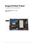
Download EVBplus2 68HC11 Development Board Getting Started Manual
Transcript
EVBplus2 68HC11 Development Board
Getting Started Manual
Version 2.45 for Ep2711E9 Rev. C board
Table of Contents
GETTING STARTED with BUFFALO Monitor …………………………………………….….………….
2
GETTING STARTED with Wytec Phantom Monitor and WBUG11 ….…………………….………….
6
Single Board Computer application ……………………………………………………….….…………..
10
ON-BOARD HARDWARE ….…………………………………………………………………………………
12
BUFFALO I/O ROUTINES …………………………………………………………………………………….
17
IMPORTANT NOTES ……….………………………………………………………………………………….
19
The Ep2711E9, a low cost and high performance development board, provides real time emulation for the
Motorola 68HC11microcontroller A and E families. It offers all useful features of the Motorola EVB board with
the BUFFALO monitor and adds numerous enhancements at an extremely low cost. It combines a complete
68HC11 development system, advanced trainer, reliable 711E9 programmer and a versatile SBC into a single
package. For engineers, it serves as a WICE in-circuit emulator development system, Motorola EVB, EVM,
EVS replacement, a convenient prototype platform, and a low cost single board computer. For students, it acts
as a user-friendly microcontroller trainer. It is as powerful as a high priced real-time in-circuit emulator, but it is
as affordable as a low cost single board computer.
Ep2711E9 includes easy-to-use and user-friendly IDE software which runs under Windows® 95, 98, 2000 and
XP. It offers fast file transfer, single-stepping, breakpoints, data watch for memory and registers, symbolic
debugging compatibility with most assemblers and compilers, and user program termination with the <Esc>
key.
Our exclusive phantom monitor™ technology preserves all interrupt vectors including RESET. The monitor
also preserve all on-chip RAM ($00-$1FF), EEPROM, and 30K external emulation RAM ($8800-$FFFF)
available for user applications - there is no pre-empted chip memory.
Because many students are taught with the Motorola BUFFALO, we installed the BUFFALO monitor in U2
(27C256 EPROM) The board can be booted from the BUFFALO monitor, so students can use the board
immediately before leaning how to use the board under Wytec’s phantom monitor.
The hardware includes a prototype area, 16 extra I/O lines in port F and G, one logic probe, on-board 16X2
LCD display with backlight, 4x4 keypad connector, 8 sensor input port, SPI port, speaker, 4-digit LED display,
potentiometer, 8 LED status indicators for port B, one 8 position DIP switch connected to port C, 3 pushbutton
switches, dual UARTs, RS485 interface, IR transceiver with on-board 38 KHz OSC, on-board 12V programming
voltage supply and 60-pin EVB/EVBU-compatible male and female connectors.
The package also includes a 7.5V 300mA wall plug-in power supply and a 6-foot DB9 cable.
The specification of the AC adapter is:
DC input:
DC output:
Current rating:
Type of plug:
110V
7.5V to 9V
300 mA to 1A
2.1mm female barrier plug, center positive
The AC adapter is only available to the countries that use 110V.
If more power is needed in a robot or other applications, the user should upgrade the AC adapter to 9V 500mA
or 9V 1A. Otherwise, the board could keep resetting itself when the VCC drops below 4.6V.
People often use different terminology. In our product menus, “Download” means to transfer a file from the PC
to the development board, while “Upload” means to transfer a file from development board to PC.
Through out the manual, left click means that you click the left button of the mouse and right click means that
you click the right button of the mouse.
Install new Ep2IDE software from CD:
If you have already installed the Ep2IDE for our WICE emulator or one of our EVBplus boards on your hard
drive, you must rename the current folder from c:\Ep2IDE to c:\Ep2IDE_old before installing new software.
The installation is automated by running the “SETUP.BAT” on the CD. It will OVERWRITE the current folder if
you don’t rename it.
After software is successfully installed, you can make a shortcut to AsmIDE.exe.
It’s very important to make a shortcut so that its target location is C:\Ep2IDE, not c:\Windows\desktop or other
locations. First, right click the Start button. Then, left click “Explorer”. Left click on C:\Ep2IDE. Right click on
1
AsmIDE.exe (an application program). Left click “Send to” and finally left click “Desktop” (do not click “COPY”
). It will create an icon named “shortcut to AsmIDE” on the desktop. You can double check the target location
by right clicking on the icon. Then, left click on “properties”. You should see that the target location is
C:\Ep2IDE. If you want to make a shortcut for AsmIDE on the Desktop, this is the correct way to do so. If you
don’t follow this method, your program may have a problem to run. Never drag the AsmIDE.exe to the desktop
folder.
The default setting of AsmIDE for the Ep2711E9 board is created in a text file named c:\Ep2IDE\AsmIDE.ini. In
the future if you get lost with all the changes, you always can copy this file into the folder c:\Ep2IDE.
GETTING STARTED with BUFFALO Monitor
The Memory Map with the BUFFALO monitor:
$0000-$00FF
$0000-$01FF
$002D-$00FF
On-chip 256 byte RAM for the 68HC11A1
On-chip 512 byte RAM for the 68HC11E1
On-chip RAM used by BUFFALO monitor
$1000-$103F
$2000-$3FFF
$4000-$5FFF
On-chip 64 control registers
External device, /CS on the pin40 of J1
8K EEPROM of U3
$6000-$61FF
not used
$6200-$63FF
$6201
$6203
$6200
$6202
65C22
PORTF
DDRF
PORTG
DDRG
$6400-$65FF
$6400
$6401
68B50
UCTRL, USTAT
UART
$6600-$67FF
$6800-$7FFF
not used
not used
$8000-$DFFF
$E000-$FFFF
RAM for user code or data
BUFFALO monitor firmware in U2
Any attempt to write to the locations ($6000-$65FF) will have unpredictable results and must be avoided in the
user program.
Because most textbooks are written for the BUFFALO monitor, the Ep2711E9 board now comes with both the
BUFFALO monitor and the Wytec Phantom Monitor installed in U2. If you have worked with the BUFFALO
monitor in the past, you can use the board right away. In fact, if you use the BUFFALO monitor with this board,
the board becomes an ordinary 68HC11 EVB board just like many other EVBs on the market today, except it
offers more on-board peripherals.
Before testing the board with the BUFFALO monitor, place a jumper on the middle position (labeled with ‘BM’
which stands for BUFFALO Monitor) of J15 and another jumper on the left position (labeled with ‘TRACE’) of
J22. To test the board, follow steps 1 through 6 below:
2
Step 1.
Plug the AC adapter into a wall outlet, and plug the DC plug at the other end into the DC jack on the lower right
corner of the Ep2711E9 board. During power up, the reset LED should blink twice and all other LEDs must be
off. If this does not occur, turn over to the Questions & Answers section of the user manual.
Step 2.
Plug the DB9 male end of the cable into the DB9 connector P2 on the upper right corner of the Ep2711E9
board,. Plug the DB9 female end of the cable into the COM1 or COM2 port of your PC. The DB9 connector P3
on the lower right side of the board is the 68HC11 SCI port that can be used by a user’s application program.
Step 3.
Press the reset button on the Ep2711E9 board and the reset LED, which is located above the switch, should
blink twice. If it does not flash, turn over to the Questions & Answers section of the user manual.
Step 4.
To invoke the AsmIDE, right click the Start button. Then left click “Explorer”. Left click on C:\Ep2IDE and
finally, double left click on AsmIDE.exe. If you have created a shortcut icon on the desktop, just double click
the icon on the desktop.
The screen is divided into two windows. The top window is for editing your source code and the bottom window
is shared by the message window and the terminal window.
Step 5:
You only need to use three commands from the AsmIDE for your 68HC11 development work. Use the File
command to edit your source code, the Build->Assemble command to assemble your source code, and the
Build->Download command to communicate with the Ep2711E9 board.
In the View->Option->Terminal Window Options menu, set the COM port as 1 or 2 to match your PC COM port.
Also, set the COM port options at 9600, N,8,1, and check the “enable the terminal window” box which will
disable Wytec hc11 tools.
In the View->Option->Assembler menu, make sure that the chip family is 68HC11 and you can also see that
the default assembler name for the hc11 is myasm11.bat, not as11.exe. This is the only change we have to
make from the original AsmIDE. If you would like to use your own assembler, you can replace the
myasm11.bat with the name of your new assembler.
If the assembler detects an error, it will show the error’s line number in the file along with an error message. Go
to the line to make a correction.
If the terminal options are set correctly, the jumper is installed on the BM position of J15, and the com port
number is correct, you should see the following sign-on message every time the reset button is pressed. If you
do not see this, the bottom window may be set for message window. Click the terminal button in the bottom
window to enable the terminal window display.
EVBplus.com: BUFFALO 3.4 - Bit User Fast Friendly Aid to Logical Operation
Press the Enter key, you will get the BUFFALO monitor prompt
>
Step 6
All sample programs are debugged and tested for your convenience. They are located in the folder
c:\Ep2IDE\Ex_BUFFL. Here are the steps to run your first sample program:
1. Click the File button to load test.asm from c:\Ep2IDE\Ex_BUFFL to view this program.
3
2. Click Build -> Assemble or click the assembler button on the toolbar to assemble your code and generate the
test.s19 file. In order to display assembler messages, the bottom window is switched to the message window.
3. Click the terminal button of the bottom window to activate the terminal window and make sure that the
BUFFALO monitor prompt ‘>’ is shown on the terminal window. If this is not the case, press the Enter key.
4. At the prompt ‘>’, type “LOAD T” <Enter>.
5. Click Build->Download and select the file c:\Ep2IDE\Ex_BUFFL\test.s19 to download it.
6. After the download is done, type G D000 to run the program.
It will run the TEST program in real time. The program will test the switches, scan the keypad, send a message
to the LCD display, adjust the LED brightness, generate music, and make LEDs PB0-PB7 act as a chaser. At
first you can press the PC0 and PC1 pushbutton switches and see a change in the PB0 and PB1 LEDs. Then,
pressing the PA0 switch will trigger the sound.
To stop the program, you have to press the reset button momentarily.
For more details on all of the sample programs, please read readme.txt in the c:\Ep2IDE\EX_BUFFL folder. All
example programs are fully debugged, so the assembler won’t generate an error report. If you have an error in
your program, you must correct it before an s19 file can be generated.
You can try to run a different example program later after you have finished reading this manual. You should
always press the reset button before downloading a new program, because a new program may not work if an
interrupt was enabled by a previous program.
Software development with the BUFFALO monitor:
We are using the AsmIDE as a terminal program in the following instructions to create your source code. If you
are using a different terminal program, the instructions may vary.
The steps to create your source code are as follows:
1 Click the File button to open an existing file or create a new file.
The memory locations from $00-$2Cfor the A family or $00-$2C and $100-$1FF for the E family are available
as user DATA RAM. The BUFFALO monitor uses the RAM locations at $2D-$FF. The 22K memory locations
from $8800 to $DFFF are available to user program CODE or DATA. In assembly language, you specify the
starting address of your CODE by an ORG statement.
You can start DATA RAM at address $00 with the statement ORG 0 followed by RAM variables, such as:
ORG
0
TEMP:
RMB
1
; reserve one byte of RAM for temp storage
XTEMP:
RMB
2
; reserve two bytes of RAM for temp storage
If your program is small, say less than 4K, you can start your program at address $D000 with the statement
ORG $D000 followed by your program, such as:
ORG
$D000
LDS
#$8FFF
; initialize stack point
It will assemble your source program and generate hex code within 4K locations from $D000 to $DFFF. If your
program is larger, you can change ORG $D000 to ORG $C000, or ORG $A000. You cannot use ORG $E000
or ORG $F000 because the BUFFALO monitor occupies the highest 8K locations ($E000-$FFFF)
After fully debugged your code, you have to relocate it to $F000-$FFFF or $E000-$FFFF and re-assemble it
again before programming it into a 68HC711E9. You don’t have to do this with the Wytec debugger, WBUG11.
Under the BUFFALO monitor, the Ep2711E9 board cannot stop your program if it’s hung in a loop. The only
way to stop it is to reset the board. The problem with resetting the board is that you will not know where the
4
68HC11 was hung. It also leaves a SWI instruction on all breakpoint addresses. You will have to re-download
your s19 file all over again.
Here is a very simple program, but it’s complete. It will flash the PB7 LED when it’s running.
For a good programming practice, you should always place the LDS instruction in the first line of your code.
PB7:
EQU
$80
; bit 7 of port B
FLS_RATE:
EQU
$8B00
; change this number will change LED flash rate
ORG
$D000
START: LDS
#$8FFF
LDX
BACK:
#$1000
BSET 4,X PB7
JSR
; turn on the PB7 LED by setting PB7=1
DELAY
BCLR 4,X PB7
JSR
DELAY
JMP
BACK
DELAY: LDY
#FLS_RATE
DLY:
DEY
BNE
; X register points to the register block
; turn off the reset LED by resetting PB7=0
DLY
RTS
END
2. Save your file frequently while editing. If you are creating a new file and giving the file a name to save, enter
the file name including the file extension, such as “test.asm”, not just “test”.
3. Click Build button-> Assemble, or click the assembler button on the toolbar to assemble your code and
generate an s19 file. If the assembler detects an error, the error message will show the line numbers in your
source code that made error. Beware that sometime (not very often, but it does happen) the freeware
assembler may indicate a wrong error line in the file and the actual line that caused error may be one line off.
WARNING: The free assembler will generate an error on the BSET, BCLR, BRSET and BSCLR instructions if
more than one commas are used in those instructions. For instance, BSET 0,X,$20 or BRSET 0,X,$20,$F000
is illegal, but BSET 0,X $20 or BESET 0,X $20 $F000 is OK. You have to use a space character to separate
fields, not a comma.
4. Go to the line and correct the errors and go back to step 3 until there are no errors.
The EVBplus2 board is an ordinary EVB board with the BUFFALO monitor, but it’s an
easy-to-use and powerful In-circuit Emulator type of development system when it’s
under the control of the Wytec Symbolic Debugger, WBUG11. If you don’t use the
WBUG11, you will not be able to exploit all of the features. Once you have used the
WBUG11, you probably would not want to use the BUFFALO again.
5
GETTING STARTED with Wytec Phantom Monitor and WBUG11
The Memory Map with the Wytec phantom monitor:
$0000-$00FF
$0000-$01FF
On-chip 256 byte RAM for the 68HC11A1
On-chip 512 byte RAM for the 68HC11E1
$0800-$0FFF
$1800-$1FFF
$1000-$103F
Wytec monitor firmware in U2
Wytec monitor firmware in U2
On-chip 64 control registers
$2000-$3FFF
$4000-$5FFF
External device, /CS on the pin40 of J1
8K EEPROM of U3
$6000-$61FF
not used
$6200-$63FF
$6201
$6203
$6200
$6202
65C22
PORTF
DDRF
PORTG
DDRG
$6400-$65FF
$6400
$6401
68B50
UCTRL, USTAT
UART
$6600-$67FF
$6800-$7FFF
not used
not used
$8000-$83FF
$8400-$FFFF
RAM used by Wytec monitor
RAM for user code or data
Any attempt to write to the locations ($6000-$83FF) will have unpredictable results and must be avoided in the
user program.
Before testing the board with the Wytec monitor, place a jumper on the top position (labeled with ‘WYTEC’
which stands for Wytec Monitor) of J15 and another jumper on the right position of J22. To test the board,
follow the steps 1 through 7 below:
Step 1.
Plug the AC adapter into a wall outlet and plug the DC plug at the other end into the DC jack on the lower right
corner of the Ep2711E9 board. During power up, the reset LED should blink 4 times and all other LEDs must
be off. If it does not flash, turn over to the Questions & Answers section of the user manual.
Step 2.
Plug the DB9 male end of the cable into the DB9 connector P2 on the upper right corner of the Ep2711E9
board. Plug the DB9 female end of the cable to the COM1 or COM2 port of your PC. The DB9 connector P3
on the lower right side of the board is the 68HC11 SCI port that can be used by a user’s application program.
6
Step 3.
Press the reset button on the Ep2711E9 board, and the reset LED, which is located above the switch, should
now blink only twice. If it does not flash, turn over to the Questions & Answers section of the user manual.
Step 4.
To invoke AsmIDE, right click the Start button. Then left click ” Explorer”. Left click on C:\Ep2IDE and double
left click on AsmIDE.exe. If you have created a shortcut icon on the desktop, just double click the icon on the
desktop.
Step 5:
The default setting of the AsmIDE for the Ep2711E9 board is created in a text file named
c:\Ep2IDE\AsmIDE.ini. In the future if you get lost with all the changes, you always can copy this file into
c:\Ep2IDE.
In the View -> Options -> Wytec hc11 tools menu, you must check the ‘Wytec Tools Enabled’ box to use the
Wytec Debugger software, WBUG11. You can change the COM port number, but you do not have to change
the baud rate, because the WBUG11 will set it at 38.4K for you. Please note that the default debugger startup
batch name is wbug11.exe, not mydebug.bat. If you left click the assembler tab under the AsmIDE options
menu, you also can see that the default assembler name for the hc11 is myasm11.bat, not as11.exe. These
are two setup changes we have to make from the original AsmIDE.
Step 6:
All sample programs are debugged and tested for your convenience and they are located in the folder
c:\Ep2IDE\Ex_WYTEC. Here are steps to run your first sample program:
1. Click the File button to load test.asm from c:\Ep2IDE\Ex_WYTEC to view the program.
2. Click Build -> Assemble or click the assembler button on the toolbar to assemble your code and generate the
test.s19 file.
3. Click Build -> Wytec hc11 tools or click the debugger button on the toolbar that will bring up a small dialog
window. You can see the file to be downloaded is c:\Ep2IDE\Ex_WYTEC\test.s19 (The current download s19
file name is always updated by the assembler).
4. Now you MUST click the “Select this file” button, which will store the file name test.s19 into a text file named
c:\Ep2IDE\Ep2IDE.txt. The debugger can automatically download the test.s19 by reading the Ep2IDE.txt when
it is invoked. This is a very important step and you must do it when you want to debug a different program.
5. Click the Debugger button and the debugger will automatically download the test program TEST.s19. The
“Programmer” button is used to program the on-chip EPROM of a 68HC711E9 and you can ignore it for the
time being.
6. At the prompt Ep6811>, enter g \start (the label is case sensitive) <Enter>.
It will run the TEST program in real time. The program will test the switches, scan the keypad, send a message
to the LCD display, emulate an IR proximity sensor, adjust the LED display brightness, generate music and
shift number 0 to F on the seven-segment display. At first, you can press the PC0 and PC1 pushbutton
switches and see the change on the PB0 and PB1 LEDs. Then, pressing the PA0 switch will generate sound.
You can press the ESC key on the PC keyboard to stop the program. If you stop the program, the speaker may
generate clicking noise because the output comparator is still interrupting the 68HC11. To stop the clicking
noise, you will need to press the reset button momentarily.
For more details on all sample programs, please read the readme.txt in the c:\Ep2IDE\Ex_WYTEC folder.
All example programs are fully debugged, so the assembler won’t generate an error. If you have an error in
your program, you must correct it before an s19 file can be generated.
7
You can try to run a different example program later after you have finished reading this manual. You should
always press the reset button before download a new program, because download may not work if interrupt
was enabled by a previous program.
Step 7:
To run another program, activate AsmIDE from the task bar at the bottom of the screen (this will minimize the
debugger window), click Build -> Wytec hc11 tools or click the debugger button on the toolbar that will bring up
the Wytec hc11 tools dialog window. Use the browser to choose the s19 file you want to download, such as
ex2.s19, then click the “Select this file” button and close the dialog window (Do not click the Debugger
button, because the debugger is already invoked). Now activate the WBUG11from the task bar and press the
F10 function key and R option, the ex2.s19 will be automatically downloaded. At the prompt Ep6811>, type “g
\start” <Enter>.
Software development with the Wytec’s Phantom Monitor:
The steps to create your source code as follows:
1 Click the File button to open an existing file or create a new file.
The memory locations from $00-$FF for the A family or $00-$1FF for the E family are available as user DATA
RAM. The Ep2711E9 board does not use the RAM locations at $2D-$FF since the BUFFALO monitor does.
The 30K memory locations from $8800 to $FFFF are available to user program CODE. In assembly language,
you specify the starting address by an ORG statement.
You can start DATA RAM at address $00 with the statement ORG 0 followed by RAM variables, such as:
ORG
0
TEMP:
RMB
1
; reserve one byte of RAM for temp storage
XTEMP:
RMB
2
; reserve two bytes of RAM for temp storage
If your program is small, say less than 4K, you can start your program at address $F000 with the statement
ORG $F000 followed by your program, such as:
ORG
$F000
LDS
#$FF
; Initialize the stack point
It will assemble your source program and generate hex code within 4K locations from $F000 to $FFFF. If your
program is larger, you can change the ORG $F000 to ORG $E000 or ORG $C000. You can use ORG $E000
or ORG $F000, because there is no BUFFALO monitor in the highest 8K locations ($E000-$FFFF)
After fully debugged your code, you do not have to relocate your code and re-assemble it. You can directly
program the s19 file into a 68HC711E9. Your code is final for stand-alone operation after finishing your
debugging session. It works just like a real time In-Circuit Emulator.
The Ep2711E9 board can stop your program if it’s hung in a loop. When you press the ESC key at the PC
keyboard, it will interrupt the Ep2711E9, but the BUFFALO monitor can’t stop the program unless you reset the
board. The problem with resetting the board is that you would not know where the 68HC11 was hung. It also
leaves SWI instructions on all breakpoint addresses resulting in having to download your s19 file all over again.
Here is a very simple program, but it’s complete.. It will flash the PB7 LED when it’s running The program
source code is similar to the tutor2.asm in the directory c:\Ep2IDE\Ex_WYTEC.
For a good programming practice, you should always place the LDS instruction in the first line of your code.
PB7:
EQU
$80
; bit 7 of port B
FLS_RATE:
EQU
$8B00
; change this number will change LED flash rate
8
ORG
START: LDS
#$FF
LDX
BACK:
$F000
; the top of A1 internal RAM
#$1000
BSET 4,X PB7
JSR
; turn on the PB7 LED by setting PB7=1
DELAY
BCLR 4,X PB7
JSR
DELAY
JMP
BACK
DELAY: LDY
#FLS_RATE
DLY:
DEY
BNE
; X register points to the register block
; turn off the reset LED by resetting PB7=0
DLY
RTS
ORG
$FFFE
FDB
START
; reset vector
END
2. Save your file frequently while editing. If you are creating a new file and giving the file a name to save, enter
the file name including the file extension, such as “test.asm”, not just “test”.
NOTE: Since the debugger is written in DOS, folder name and filename should not be longer than 8
characters.
3. Click Build -> Assemble or click the assembler button on the toolbar to assemble your code. IF your code
has no errors, it will generate an s19 file, a listing file and a symbol file. If the assembler detects an error, the
error message will show the line numbers of your source code that caused error. Beware that sometime (not
very often, but it does happen) the freeware assembler may indicate a wrong error line in the file and the actual
line that caused error may be one line off.
4. Correct the errors and go back to step 3, until there are no errors.
5. After your code is successfully assembled, you click Build -> Wytec hc11 tools-> “select this file” button to
update the file c:\Ep2IDE\Ep2IDE.txt for the debugger.
6. Close the dialog window and activate the WBUG11 from the task bar. Press the F10 function key and the
R option. The debugger will automatically download 3 files, namely YOUR_FILENAME.S19,
YOUR_FILENAME.SYM, and YOUR_FILENAME.PAR. The S19 file is the hex code. The SYM file is the
symbol file, so you can use symbols in commands instead of hex numbers. The PAR file is the parameter file
that includes the EEPROM programming enable/disable flag, INIT, TMSK2, OPTION, and BPROT register
values. The PAR file also includes breakpoint addresses and the memory display addresses.
The assembler does not make a PAR file, but the debugger does. When you first invoke the debugger, a PAR
file does not exist. When you exit the debugger, the debugger will create one by saving the current settings.
The PAR file is automatically saved after you exit the debugging session.
After that, the par file will always exist. Also, the Write command of the debugger can create a PAR file. After
invoking the Write command in the debugger, it will prompt you to enter a choice among U, S, and P options.
Choose the P option and give a full file name such as test.par. It will make a PAR file for you.
The most useful feature of the PAR file is its ability to remember the INIT register value. Suppose you relocate
the 68HC11 control registers to a different memory block by changing the value of the INIT register in the
beginning of your source program (the INIT register can only be changed in the first 64 E cycles in expanded
mode), you have to use the Init command to change the INIT register to match that value before running your
program under the WBUG11, otherwise your program will not run. When the PAR file is loaded, it will generate
a system reset and force the 68HC11 to take the new INIT register value from the PAR file. For more
information, see the Questions & Answers section of the user manual.
9
7. When the download is finished and you are prompted with Ep6811>, you can run your program by entering
“go \start” where the start is the label of the starting address in your source code or enter G F000 if you know
the starting address is $F000, but do not enter command too soon. After download, the PC will reset the board.
During the reset, there will be some communication between the PC and the board. If you enter the command
too soon, it could disrupt the communication and you will get an error message.
In the command line, ALL NUMBERS ARE HEXADECIMAL and the $ sign is not needed. Also you should
notice that the label \start has the back slash in the front. All hex numbers may be substituted by symbols
starting with the backslash ‘\’. For more information read the Command format section in the user manual.
8. During the debugging session, if you want to modify your source code, you don’t have to exit the debugger.
You can activate AsmIDE to edit your code and save your new code with the same file name. Then click Build > Assemble or click the assemble button on the toolbar to assemble the code. A new S19 file should be
generated. Because you did not change the file name, you don’t have to click the “Select this file” button
again. The only thing you have to do is to click the “WBUG11” button at the task bar at the bottom line of the
screen to activate debugger window. Then enter the F10 key and the R option to download your files and start
debugging again.
Single Board Computer application:
The Memory Map in Single Board Computer application:
$0000-$00FF
$0000-$01FF
On-chip 256 byte RAM for the 68HC11A1
On-chip 512 byte RAM for the 68HC11E1
$0800-$0FFF
$1800-$1FFF
$1000-$103F
Wytec monitor in U2, some subroutines are callable from user programs
Wytec monitor in U2, some subroutines are callable from user programs
On-chip 64 control registers
$2000-$3FFF
$4000-$5FFF
External device, /CS on the pin40 of J1
not used
$6000-$61FF
not used
$6200-$63FF
$6201
$6203
$6200
$6202
65C22
PORTF
DDRF
PORTG
DDRG
$6400-$65FF
$6400
$6401
68B50
UCTRL, USTAT
UART
$6600-$67FF
$6800-$7FFF
not used
not used
$8000-$DFFF
$E000-$FFFF
RAM for user data
User code in U3 (8K EEPROM)
10
Program 8K EEPROM in U3 and 512 bytes of on-chip EEPROM:
You can program 8K EEPROM in U3 and 512-bytes of on-chip EEPROM ($B600-B7FF) under control of the
Wytec debugger WBUG11. Use the Load command as described on page 10 of the user manual. The
instructions will be shown on the screen when Load command is entered.
If you want to use the board as a SBC, you can program your application s19 file into U3 (8K EEPROM). After
programming the chip, place a jumper on the bottom position of J15 (at the left side of the speaker). It will
completely bypass both the Wytec’s proprietary phantom monitor and the BUFFALO monitor. The address
range of U3 is changed from $4000-$5FFF to $E000-$FFFF and the address range of U4 is changed from
$8000-$FFFF to $8000-$DFFF. The program code will auto start from U3 after reset or power up.
Before programming, the jumper on J15 must be placed on the “WYTEC” position and the jumper on J9
must be placed on the “RUN” position ( not the “PRG” position).
1. Move the jumper to the right position on the J21 to enable EEPROM write.
2. Enter Load command and select the E option to download an s19 file into the U3.
3. Enter test.s19 as the file name to be downloaded.
4. When the programming cycle starts, the PB0-PB7 LEDs will act as a binary counter.
5. The programming is done when LEDs stop counting.
6. Move the jumper to the left position on J21 to write-protect U3.
7. Move the jumper on J15 to the bottom position (labeled with the ‘U3’).
8. Press the reset button, your application program should run.
Before programming you have to make sure that the jumper on J21 is on the right side to enable EEPROM
write, otherwise the programming process will not continue. After programming, place the jumper on the left
side of J21 to write-protect the EEPROM, otherwise the EEPROM could lose data quite easily after running a
bad program during a debugging session.
The procedures to program the 512-byte on-chip EEPROM ($B600-B7FF) are the same as the above steps
except for step 2. Select option B instead of option E after the Load command id entered.
About AsmIDE:
AsmIDE is written by Eric Engler and it’s simple and easy to use. It offers all the basic features that you need to
learn 68HC11 programming with this board. Sometimes a simple IDE may not be a bad idea; at least students
don’t need to spend too much time to learn how to use the IDE, so they will have more time to focus on learning
the 68HC11which may be their main objective of taking a course. If you spend a lot of time to master a bloated
IDE and you don’t use it for a while, you will probably forget how to use it anyway. So, why spend time on
something that you are going to lose? On the contrary, a simple, easy to use IDE saves you time and will be
much easier to remember how to use even after an extended period of time.
The most valuable asset of the Ep2711E9 board is the WICE debugger, WBUG11. Some boards that you can
buy today may have a bloated IDE, but you probably would get a BUFFALO type monitor for debugging.
Using your own assembler or editor for WBUG11:
If you would prefer to use your own assembler or editor instead of AsmIDE, you can use AsmIDE for launching
the WBUG11. The full path name of the file that you work on must agree with the file name shown on the
Wytec hc11 tools dialog window, otherwise the WBUG11 will not be able to locate your s19 file to be
downloaded.
Make your own monitor:
11
If you want to make your own monitor to install a high language source level debugger, you can treat your
monitor as an application and program it into U3 (8K EEPROM) according to the instructions shown on the
previous page.
Using the board as a 68HC711E9 programmer:
If you need to program a 68HC711E9, you can use this board as a 68HC711E9 programmer, but only under
control of the Wytec debugger WBUG11. You must make sure that the program is fully debugged. To activate
the programmer, click Build -> Wytec hc11 tools, or click the debugger button on the toolbar that will bring up a
small dialog window. If the current downloaded s19 file is correctly shown in the dialog window, click the
“Select this file” button and then click the “programmer” button to program the 68HC711E9. The
programming is done in bootstrap mode and the programming instructions will be displayed on the screen step
by step. The memory addresses range for the 68HC711E9 is from $D000 to $FFFF. If your S19 file contains
addresses outside of this range, an error message will be generated and the chip will not be programmed. If
your assembler or C compiler generates an s19 file with some extra RAM addresses, you must use an editor to
delete those addresses.
During the programming, the data will be automatically verified.
The 52-pin PLCC socket is not built for a high volume production programmer. It will not last much longer than
100 insertions. When the contacts of the PLCC socket are worn, you can use a fine dental tool to pry up the
contacts a little bit to extend its life considerably.
ON-BOARD HARDWARE
Port B and port C are used for address and data buses. They are not available as I/O ports during debugging
session in expanded mode, but they are emulated by PRU chip 68HC24. The PRU stands for port replacement
unit.
Port B is an output port and each port B line is monitored by a LED. Port C is a bi-directional I/O port and it is
connected to an 8-position DIPswitch. The DIPswitch is connected to GND via eight 4.7K resistors, so it’s not
dead short to GND. When port C is programmed as an output port, the DIPswitch setting is ignored.
The PA0 switch is used as a general input switch, except during power up. During power up, press and hold
the PA0 switch while pressing the RESET button will force the 68HC11 to enter test mode. In test mode, the
configure register can be modified. PA4 and PA6 headers are the outputs of Output Comparator 5 and 4. They
can be used to drive robot servos.
Port E is an 8-bit ADC or a general input port. The trimmer VR1 is connected to the PE7 input of the ADC port
via the cut-trace J10. The trace can be cut if PE7 must be used by target circuit for a different purpose.
An on-board logic probe LED is connected to pin 55 of the female socket connector P1F and can be used to
monitor high or low status at any point of the circuit as a logic probe.
U16, LTC1262 or MAX662, provides a 12 V programming voltage for the 68HC711E9.
U18, 74HC14, generates 38.4K baud for U5, 68B50, and it also provides 38KHz square wave to IR transmitter.
U9, SN75176, converts the TTL signal from the SCI to RS485 differential signals and visa versa.
Two RJ12 jacks, JK1 and JK2, can be used to daisy chain many Ep2711E9 boards together for a network
application. Connections on JK1 and JK2 are identical, so either one can be input or output.
Two I/O ports, port F and port G are added through U1, VIA 65C22. These are bi-directional ports. Port F and
port G are port A and port B of the 65C22, respectively. The address locations for all ports are as follows:
12
PORTF
DDRF
PORTG
DDRG
$6201
$6203
$6200
$6202
; 1=OUTPUT, 0=INPUT
; 1=OUTPUT, 0=INPUT
CA2 output from the 65C22 is used to control direction of RS485 communication. If CA2=0, RS485 port, U9
DS75176, is set for receiver port; If CA2=1, RS485 port, U9 DS75176, is set for transmitter port.
CA2=0
CA2=1
RS485 receiver port
RS485 transmitter port
For users’ convenience, there are two subroutines added to control CA2. User can call RS485_RECV at $0800
to reset CA2 to 0, or RS485_XMIT at $0803 to set CA2 to 1.
The following are all I/O subroutines in Wytec monitor that are callable from a user’s application program:
RS485_RECV:
RS485_XMIT:
GET_DATE:
GET_TIME:
OUTSTRG00:
LCD_INI:
LCD_LINE1:
LCD_LINE2:
SEL_INST:
SEL_DATA:
WRT_PULSE:
ORG
$0800
; EVBplus2 Rev. C board I/O routines
RMB
RMB
RMB
RMB
RMB
RMB
RMB
RMB
RMB
RMB
RMB
3
3
3
3
3
3
3
3
3
3
3
; enables RS485 receiving mode
; enables RS485 transmitting mode
; gets current date from PTC
; gets current time from PC
; outputs a string terminated by 0
; initializes the 16x2 LCD module
; displays 16 char on the first line
; displays 16 char on the second line
; selects instruction before writing the LCD module
; selects data before writing the LCD module
; generates a write pulse to the LCD module
The circuit is designed in such way that the value of all resistors and capacitors are not critical, they can be off 50% or +100%.
How to use port F:
Port F is an 8-bit bi-directional port. Its primary usage is for an LCD display module. If the port is not used as
an LCD display, it can be used as a general-purpose I/O port that can be accessed via J2 or J3.
The pinouts of the J3 is as follows:
Pin 1
Pin 2
Pin 3
Pin 4
Pin 5
Pin 6
Pin 7
Pin 8
Pin 9
Pin 10
Pin 11
Pin 12
Pin 13
Pin 14
GND
VCC (5V)
Via a 100 Ohm resistor to GND
PF0
GND
PF1
Not used
Not used
PF2
PF3
PF4
PF5
PF6
PF7
RS pin for LCD module
EN pin for LCD module
DB4 pin for LCD module
DB5 pin for LCD module
DB6 pin for LCD module
DB7 pin for LCD module
13
Pin 15 Via an 18 Ohm resistor to VCC LED backlight for LCD module
Pin 16 GND
The pinouts of the J2 is as follows
Pin 1
Pin 3
Pin 5
Pin 7
Pin 9
Pin 11
Pin 13
Pin 15
Pin 17
Pin 19
PF7
PF6
PF5
PF4
PF3
PF2
PF1
PF0
VCC
GND
Pin 2
Pin 4
Pin 6
Pin 8
Pin 10
Pin 12
Pin 14
Pin 16
Pin 18
Pin 20
PG7
PG6
PG5
PG4
PG3
PG2
PG1
PG0
VCC
GND
How to use port G:
Port G is an 8-bit bi-directional port. Its primary usage is for a 4X4 keypad interface. If the port is not used as a
keypad interface, it can be used as a general-purpose I/O port that can be accessed via J2 or J6.
The pinouts of the J6 is as follows:
Pin 1
Pin 2
Pin 3
Pin 4
Pin 5
Pin 6
Pin 7
Pin 8
PG0
PG1
PG2
PG3
PG4
PG5
PG6
PG7
connects ROW0 of the keypad
connects ROW1 of the keypad
connects ROW2 of the keypad
connects ROW3 of the keypad
connects COL0 of the keypad
connects COL1 of the keypad
connects COL2 of the keypad
connects COL3 of the keypad
Keypad interface
PG0 connects ROW0 of the keypad via pin 1 of the 8-pin keypad header
PG1 connects ROW1 of the keypad via pin 2 of the 8-pin keypad header
PG2 connects ROW2 of the keypad via pin 3 of the 8-pin keypad header
PG3 connects ROW3 of the keypad via pin 4 of the 8-pin keypad header
PG4 connects COL0 of the keypad via pin 5 of the 8-pin keypad header
PG5 connects COL1 of the keypad via pin 6 of the 8-pin keypad header
PG6 connects COL2 of the keypad via pin 7 of the 8-pin keypad header
PG7 connects COL3 of the keypad via pin 8 of the 8-pin keypad header
PG0-PG7 has a 100K pull-up resistor in each line.
The keypad scan routine sets PG3 low, PG0,PG1,PG2 high, and then test the PG4-PG7
If no key is down, PG4-PG7 remain high.
If PG7 = low, the key 15 is down.
If PG6 = low, the key 14 is down.
If PG5 = low, the key 13 is down.
If PG4 = low, the key 12 is down.
The keypad scan routine then sets PG2 low, PG0,PG1,PG3 high then test the PG4-PG7
If no key is down, PG4-PG7 remain high.
If PG7 = low, the key 11 is down.
If PG6 = low, the key 10 is down.
14
If PG5 = low, the key 9 is down.
If PG4 = low, the key 8 is down.
The keypad scan routine then sets PG1 low, PG0,PG2,PG3 high then test the PG4-PG7
If no key is down, PG4-PG7 remain high.
If PG7 = low, the key 7 is down.
If PG6 = low, the key 6 is down.
If PG5 = low, the key 5 is down.
If PG4 = low, the key 4 is down.
The keypad scan routine then sets PG0 low, PG1,PG2,PG3 high then test the PG4-PG7
If no key is down, PG4-PG7 remain high.
If PG7 = low, the key 3 is down.
If PG6 = low, the key 2 is down.
If PG5 = low, the key 1 is down.
If PG4 = low, the key 0 is down.
SPI port pinouts are as follows:
Pin 1
Pin 3
Pin 5
Pin 7
Pin 9
VCC (5V)
PF2 (LOAD)
PF3 ( STROBE)
not used
GND
Pin 2
Pin 4
Pin 6
Pin 8
Pin 10
VCC (5V)
PD2 (SPI DATA IN)
PD3 (SPI DATA OUT from 68HC11)
PD4 (CLOCK)
GND
All on-board jumpers:
J1
J2
J3
J4
J5
40 pin logic analyzer connector, Motorola 68HC11 EVM compatible
Port F and Port G, total 16 bits, the left side is port F and the right side is port G
LCD port
SPI connector
Mode selector. MODEA and MODEB jumpers are not used in debugging sessions. They can be used
for programming the 68HC711E9 OTP part in bootstrap mode.
J6
J7
J8
4 X 4 keypad interface
RS485 direction control, it’s a cut-off trace
HC11 SCI receiver source selector (numbering from top to bottom)
1= SCI PD0 receives signal from your target system via P1 or P1F
2= SCI PD0 receives signal from the P3, DB9 connector for RS232 input
3= SCI PD0 receives signal from the JK1 or JK2 (RJ12 jacks) for RS485 input
4= SCI PD0 receives signal from the on-board IR receiver
J9
RUN/PRG jumper, it is used for selecting operating mode
Jumper is on the right position for programming the 68HC711E9 chip
Jumper is on the left position for debugging your code
J10
J11
Connects VR1 trimmer pot to PE7 of ADC, It’s a cut-off trace
Analog voltage reference selector.
When jumpers are on the right position, the on-board 5V DC is the reference voltage
When jumpers are on the left position, user target provides the reference voltage
It’s connected to the on-board 5V DC reference voltage and GND via two cut-off traces.
J12
Clock selector.
When jumper is on the right position (labeled with ‘INT’), clock is provided by the on-board crystal.
When jumper is on the left position, (labeled with ‘EXT’), user target provides a HC compatible clock
source.
Clock output. It’s not installed. If it’s installed, the clock output of the 68HC11(pin 8) can be a clock
source of user target board.
Enables speaker. The speaker is driven by PA5, Output Comparator 3 through jumper J14.
J13
J14
15
J15
J16
J17
J18
J19
J20
J21
J22
It’s connected by a cut-off trace.
Monitor selector. Place a jumper on the top position for Wytec monitor, the middle position for
BUFFALO monitor and the bottom position for auto-starting program in U3.
Connects the 68HC11 SCI’s PD1 to all communication hardware (RS232, RS485 and IR transceiver)
on this development board. It’s connected by a cut-off trace.
IR transceiver control source selector.
When jumpers are placed on the upper position (labeled with ‘SCI’), HC11’s PD1drives IR transmitter
and HC11’s PD0 receives data from IR receiver. PD0 and PD1 can be general I/O lines or SCI.
.
When jumpers are placed on the lower position (labeled with ‘PA26’), HC11’s PA6 drives IR transmitter
and PA2 receives data from IR receiver.
Enables 7 segment LED display driver U11, 74HC367. If 7 segment LED display is not needed in an
application, remove this jumper to turn off display and save power.
Enables LCD backlight. If LCD display is not needed in an application, remove this jumper to turn off
backlight and save power.
12V output from U16 (5V-12V converter).
U3 EEPROM write protect, place a jumper on the left position to disable (write-protect) EEPROM
programming. Place a jumper on the right position to enable EEPROM programming.
Enables BUFFALO trace function.
When jumper is on the left position, PA3 is connected to XIRQ to enable single-stepping operation.
When jumper is on the right position, PA3 is disconnected from the XIRQ.
Sensor port: The top line is signal, the middle line is VCC and the bottom line is GND. Digital sensors can be
connected to PA0,PA1,PA2 and PA7. Analog sensor can be connected to PE0-PE3. There is a 100K pullup
resistor on each sensor input.
P3 DB9 female connector is configured as a DCE device and it can be directly connected to your PC ‘s COM
port.
Application Circuit Corner (ACC) and Solderless Breadboard:
The footprints of four popular 68HC11 applications are laid out on the upper left corner of the PC board. The
ACC consists of a DS1302 Real Time Clock with a battery backup, a DS1620 Digital Thermometer and
Thermostat, a 12V DPDT relay and a L293D Motor driver. . In the future we will offer a kit for your experiments
and each circuit in a separate kit. With these application circuits, this board can easily be transformed into a
complete platform for useful applications.
The lower left corner is a small solderless breadboard. All I/O signals are available on the 60 pin female
connector P1F. The 60 pin male header P1 can be used to connect all user I/O boards made for the original
Motorola 68HC11 EVB board. Use the breadboard for prototyping or solder components directly to the board if
you remove the breadboard. The Ep2711E9 board is not complete without a breadboard.
The schematic for the PC board is divided into sch1.jpg, sch2.jpg and sch3.jpg. The ACC schematic is in
sch_acc.jpg.
New RF transceiver and phone jacks:
The Rev C board incorporates circuit layout under the breadboard for a RF transceiver, a RJ12 jack and a RJ45
jack. In the future we will offer a kit for your RF experiment. The schematic is in RF_jack.jpg.
16
BUFFALO I/O routines.
Many 68HC11 books have example programs that access BUFFALO I/O routines. The BUFFALO I/O routines
are located at $FFA0-$FFCF. When using it with the Wytec debugger WBUG11, the BUFFALO I/O functions
are duplicated at $0FA0-$0FCF.
Following are the BUFFALO I/O routines’ function description and jumper table:
ORG
UPCASE
WCHEK
DCHEK
INIT
INPUT
OUTPUT
OUTLHLF
OUTRHLF
OUTA
OUT1BYT
OUT1BSP
OUT2BSP
OUTCRLF
OUTSTRG
OUTSTRG0
INCHAR
$0FA0
convert the character in A to uppercase
test the character in A for white space and returns with the Z bit set if A is a
white space (Space, comma, tab)
test the character in A for white space and returns with the Z bit set if A is a
carriage return or white space (Space, comma, tab)
initialize SCI, is not needed with the EP2711E9 board
reads PC keyboard input
writes the character in the A to CRT display
converts 4 most Significant Bit of A to ASCII and Writes it to CRT display
converts 4 most Significant Bit of A to ASCII and Writes it to CRT display
output ASCII character in A to CRT display
converts the binary byte that is pointed to by X register to 2 ASCII bytes and
write them to CRT display
it’s OUT1BYT followed by sending a space to CRT display
converts the binary word (2 bytes) that is pointed to by X register to 4 ASCII
bytes and write them followed a space to CRT display
write carriage return, line feed to CRT display.
it’s OUTCRLF followed by writing the ASCII string that is pointed to by
X register to CRT display and until character is $04
it’s OUTSTRG without writing leading carriage return & line feed to CRT display
waits for an ASCII character from keyboard and put it in accumulator A
Jump Table
$0FA0
$0FA3
$0FA6
$0FA9
$0FAC
$0FAF
$0FB2
$0FB5
$0FB8
$0FBB
$0FBE
$0FC1
$0FC4
$0FC7
$0FCA
$0FCD
UPCASE
WCHEK
DCHEK
INIT
INPUT
OUTPUT
OUTLHLF
OUTRHLF
OUTA
OUT1BYT
OUT1BSP
OUT2BSP
OUTCRLF
OUTSTRG
OUTSTRG0
INCHAR
17
We have added several I/O routines in the beginning of our Phantom Monitor.
Following are the Phantom Monitor’s I/O routines’ function description and jumper table starting at $0800:
ORG
$0800
RS485_RECV
RS485_XMIT
GET_DATE
sets RS485 port to receiver mode.
sets RS485 port to transmitter mode
X register points to a 10 byte RAM block before calling this subroutine, it returns date
information of host PC in the format of MM-DD-YYYY.
GET_TIME
X register points to an 11 byte RAM block before calling this subroutine, it returns time
information of host PC in the format of HH:MM:SS AM or HH:MM:SS PM.
OUTSTRG00
It’s OUTSTRG0 except the ending character is $00, instead of $04.
LCD_INI
initialize a 16x2 LCD display module
LCD_LINE1
displays 16 characters on the first line of a 16X2 LCD display module
LCD_LINE2
displays 16 characters on the second line of a 16X2 LCD display module
SEL_INST
selects instruction before writing a LCD module
SEL_DATA
selects data before writing a LCD module
WRT_PULSE
generates a write pulse for LCD module
SEVEN_SEGMENT: converts Accu A to its segment pattern, bit 7 of the Accu A = Decimal Point
of the 4 digit LED display module.
Jump Table
$0800
$0803
$0806
$0809
$080C
$080F
$0812
$0815
$0818
$081B
$081E
$0821
RS485_RECV
RS485_XMIT
GET_DATE
GET_TIME
OUTSTRG00
LCD_INI
LCD_LINE1
LCD_LINE2
SEL_INST
SEL_DATA
WRT_PULSE
SEVEN_SEGMENT
The subroutine SEVEN_SEGMENT is a conversion routine that converts a hex numbers to its seven segment
pattern. The hex number range is from $00 to $20.
At entry, A= hex #
A=$00
A=$01
A=$02
A=$03
A=$04
A=$05
A=$06
A=$07
A=$08
A=$09
A=$0A
A=$0B
A=$0C
A=$0D
A=$0E
A=$0F
At exit, A=segment pattern
A=$3F
A=$06
A=$5B
A=$4F
A=$66
A=$6D
A=$7D
A=$07
A=$7F
A=$6F
A=$77
A=$7C
A=$39
A=$5E
A=$79
A=$71
The letter or number to be formed by the segment pattern
0
1
2
3
4
5
6
7
8
9
A
B
C
D
E
F
18
A=$10
A=$11
A=$12
A=$13
A=$14
A=$15
A=$16
A=$17
A=$18
A=$19
A=$1A
A=$1B
A=$1C
A=$1D
A=$1E
A=$1F
A=$3D
A=$76
A=$74
A=$1E
A=$38
A=$54
A=$63
A=$5C
A=$73
A=$50
A=$78
A=$3E
A=$1C
A=$6E
A=$08
A=$40
G
H
h
J
L
n
o
o
P
r
t
U
u
Y
_
--
A=$20
A=$00
blank
IMPORTANT NOTES
The following are some important notes that you should know and they may save your time:
1. Things to do if the board does not work.
Many little mistakes can cause a big problem, especially for new beginners. For instance, you may debug your
code in expanded mode, but MODEB and MODEA are set for bootstrap. If the jumper on the J19 is missing,
LCD backlight won’t work and if the jumper on J18 is missing, 7-segment display won’t be lit.
Before troubleshooting the board, you must apply power to the board. Press the reset button, the LED should
blink twice. If it does not blink, the board may not have 5V DC. Use a DMM to check voltages at the VCC test
point. Sometimes it may be caused by a bad AC adapter or the AC adapter may not even plugged in.
Sometime the Config register has a wrong value, but the 68HC11 chip is still good.
To determine if the board malfunctions, you can restore the board jumper settings to the original default settings
when you receiving the board. The default settings are as follows:
J5
J8
Mode selector. No jumper installed.
HC11 SCI receiver source selector
The jumper is on the bottom position (labeled with ‘IR’)
J9
J15
RUN/PRG jumper is used for selecting operating mode.
The jumper is placed on the left position for debugging your code.
Clock selector.
The jumper is placed on the right position (labeled with ‘INT’), the clock is provided by on-board crystal.
Monitor selector. The jumper is placed on the middle position for BUFFALO monitor.
J17
IR transceiver control source selector.
J18
J19
J22
The jumpers are placed on the upper position (labeled with ‘SCI’), HC11’s PD1 drives IR transmitter
and HC11’s PD0 receives data from IR receiver.
Enables 7 segment LED display driver U11, 74HC367. The jumper is installed on this header.
Enables LCD backlight. The jumper is installed on this header.
Enables BUFFALO trace function. The jumper is placed on the left position.
J12
19
If all above settings are correct, when you press the reset button, the reset LED should blink twice. If this does
not flash, you can try to enter test mode to determine if the 68HC11 chip is bad. Sometimes the Configuration
register has a wrong value, but the 68HC11 chip is still good and will work in test mode. In test mode you can
use the F8 function key to re-program the value of the Configuration register to $0D. If you cannot enter test
mode, the 68HC11 is defective.
To enter test mode, you have to change the jumper on J15 to the top position to enable the Wytec monitor.
Then press the reset button while holding down the PA0 switch to enter test mode. The LED should flash twice.
If it does not flash, the 68HC11 is probably dead.
The crystal is not soldered to the board and it’s held by two machine pins. If you want to change the crystal,
just unplug it and replace it with a new frequency, such as 9.8304 MHz. Don’t cut the crystal’s leads too short.
If it’s shorter than ¼”, its metal case could short the two machine pins.
2. Always reset the board before downloading a new program.
If the previous application program that you ran was aborted, then you may need to reset the board before
downloading a new application program. The reset action will disable the interrupt that was enabled by the
previous application. If the interrupt was caused by a timer and is not disabled, the timer interrupt will continue
even it’s not called for in your new application program. The result will be unpredictable.
3. Disconnect LCD module from the bottom of the main PCB first.
The LCD display module has 2 supporting nylon spacers. They fit tighter with the LCD module PCB than with
the main PCB. So if you need to remove the LCD module from the board, the spacers should stay with the
LCD module. That means you should use a pair of pliers to push up the spacers from the bottom of the main
PCB to separate the spacers from the main PCB. Once the spacers are loose from the main PCB, you can
easily unplug the LCD module.
4. Keep folder name and file name not to exceed 8 characters when working under Wytec Monitor.
The Wytec debugger is a DOS application, so keep folder and file names short, otherwise file download won’t
work.
20


