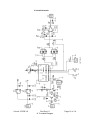
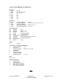
1
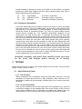
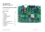
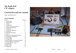
X-Lock VFO Stabiliser
User Manual
CONTENTS
1
INTRODUCTION
2
2
PREPARATION
2
3
CIRCUIT DESCRIPTION
3
4
ASSEMBLY
5
5
TESTING
7
6
CONFIGURATION AND SET UP
8
APPENDIX A
Troubleshooting
16 Chestnut Close
Culgaith
PENRITH
Cumbria
CA10 1QX
UK
1 Introduction
Thank you for purchasing the Cumbria Designs X-Lock kit. We hope that you
enjoy constructing this kit and find many uses for this feature rich design. This
manual describes the assembly and operation of the X-Lock kit, even if you are a
seasoned constructor, we respectfully ask that you read this manual and
familiarise yourself with the instructions and kit contents before commencing
construction. If assembled carefully, this unit will provide many years of reliable
service.
The Cumbria Designs Team
________________________________________________________________
2 Preparation
2.1
Tools
We recommend that the following tools
are used during assembly and testing;
25W fine tipped soldering
60/40 Rosin cored solder
5” or smaller diagonal side cutters
2.4
Small pointed nosed pliers
Solder sucker (just in case!)
Multimeter
2.2
Conventions
The following symbols are used within
the assembly instructions to draw
attention to critical steps such as
component orientation and anti-static
precautions. The associated narrative
describes the action required.
!
Critical Step
Static Sensitive
Don’t be tempted to rush the
construction, even though this is a
relatively simple kit, a wrongly placed
component can provide hours of
frustrating fault finding. Also, as this kit
uses a double sided Printed Circuit
Board (PCB) with through plating,
removal of a wrongly soldered part
can be difficult. Follow the assembly
instructions
carefully
to
avoid
mistakes.
All parts carry a coded identity to
describe their values. It is important to
be able to recognise these during
assembly. Capacitors have their value
printed numerically, e.g. 104 = 100nF,
103 = 10nF etc. Resistors have their
values represented by coloured bands
– this is a frequent source of
confusion!
To simplify component identification,
the parts list carries the identities of
each component as it appears on the
device. For resistors the colour coding
is given. This should be referred to
during assembly to ensure the right
parts are placed in their respective
positions on the PCB.
2.5
2.3
Assembly
The production of a successful
finished working kit is dependent upon
careful component handling, careful
placement and good soldering!
X-Lock 3 PCB 3.0
Component Identification
Component Leads
Many of the passive components will
require their leads to be formed to
align with the holes on the PCB. This
mainly applies to the axial parts such
as resistors and diodes. Forming
Doc Rev1.2
© Cumbria Designs
Page 2 of 14
component leads is easily done with a
pair of pointed nose pliers and using
the hole spacing on the PCB as a
measure. Alternatively, small formers
made from scrap off cuts of Vero
board etc make ideal templates that
produce consistent results. Some
parts, such as variable resistors, have
preformed leads designed for machine
assembly.
These
will
require
straightening to align with the board
layout. Again, a pair of pointed nose
pliers should be used to carefully
flatten the factory performing to
produce straight leads.
2.6
Soldering
Before applying solder check carefully
that the component you have
placed is in the right position! This
is a through plated double sided
board. Whilst some of the pads are
very small, the area presented by the
through plating is more than adequate
to allow good solder flow to form
mechanically strong good electrical
joints. These can be difficult to undo,
please double check!
•
This is the bit that can trip up even
experienced constructors. For the
solder to fuse with the surfaces to be
joined it is necessary for them to be
hot – but not so hot as to damage the
parts! It’s a simple as 1-2-3;
1. Place the tip of the iron against
the joint, hold it there briefly to
bring the metal surfaces up to
temperature.
2. Apply the solder allowing it to
flow
smoothly
onto
the
surfaces.
3. Remove the iron and inspect
the new joint.
The finished joint should have a
smooth shiny coating of solder. If the
joint is dull grey or has formed a
spherical “blob”, apply the iron to the
joint, remove the old solder with a
solder sucker and re-solder.
3 Circuit Description
3.1
The majority of problems are likely to
be caused by soldering faults. These
can sometimes be difficult to find. Here
are some basic golden rules that will
help you to avoid poor solder joints;
•
Clean Iron
Make sure your soldering iron tip is in
good condition and tinned. A small
moistened pad for cleaning tips,
regularly used to wipe off excess
solder and flux, will ensure that your
iron performs well. Remember to tin
the iron immediately after each wipe.
•
Clean Leads and Pads
All of the component leads and PCB
pads in this kit are pre-tinned and
should not need cleaning before
soldering. Please ensure that parts are
handled so as to avoid contamination
with grease or fingerprints.
X-Lock 3 PCB 3.0
Soldering
General
The X-Lock is a micro-controller based
frequency stabiliser designed as an
easily applied “add-on” to enhance the
frequency stability of existing free
running variable frequency oscillators
(VFOs). This compact module will
accept an input signal with a range of
a few tens of kHz to over 50MHz and
produce a variable correction voltage
to drive a simple drift compensation
circuit fitted to the host oscillator. To
minimise the risk of introducing digital
noise to the host oscillator, the
analogue section of the X-Lock
operates from its own regulated supply
and is optically coupled to the digital
control circuitry.
Two tactile switches allow the key
parameters to be adjusted after
installation. A tri-colour LED indicates
operational and diagnostic status.
Doc Rev1.2
© Cumbria Designs
Page 3 of 14
3.2
Theory of Operation
The Cumbria Designs X-Lock is a
derivative of the “Huff-Puff” stabiliser
system devised by the late Klaas
Spaargaren PA0KSB in the 1970’s.
The x-Lock compares the frequency of
the controlled oscillator with a crystal
reference (hence X-Lock = Xtal-lock),
to produce a correction signal which is
used adjust the frequency of the
oscillator. The action is to hold the
frequency of the controlled oscillator
frequency at 10Hz lock points.
At the heart of the X-Lock is a 16F628
processor (IC3) which performs all of
the
measurement
and
control
operations. The input signal is buffered
by Q1 and amplified by Q2 before
being presented to the input of the
processor on pin 12. The gate circuit is
internal to the processor and operates
over a 100mSec period to provide a
count resolution of 10Hz. The value of
each measurement is compared with
that of the previous and if the
difference is equal to or less than
50Hz, the 16F628 processor will
generate a correction signal. This
takes the form of variable duration
control pulses on the Up and Down
signal lines from the processor to drive
LED’s within the opto-coupler, IC4.
The opto-coupler transistors are
operated by the LEDs to charge or
discharge the voltage stored in the
loop filter R9, C11 and C15. The time
constant of the loop filter is very long
resulting in a slow rate of change of
the control voltage. To ensure that the
control voltage starts at centre rail, a
reset switch formed by FET Q3 is
enabled by the processor on power
on. This ensures that C11 and C15 are
fully discharged. Once Q3 is turned
off, the capacitors re-charge via R5 to
set a centre rail output voltage. In the
unlikely event that the loop control
voltage becomes “saturated” after a
prolonged period of operation, the
X-Lock 3 PCB 3.0
control voltage can be set to centre
again by briefly powering the X-Lock
on and off to operate the Q3 reset
switch. The host VFO will need to be
retuned following a reset.
A rail to rail operational amplifier IC5,
buffers the filter, providing a low
impedance source for the control
voltage
to
drive
the
external
compensation varactor. Whilst the
varactor circuit exhibits a very high
input impedance at DC, the low
impedance of the operational amplifier
output stage reduces the effects of
stray voltages on the control voltage
line. A simple RC filter (R10 and C16),
decouples the control signal at the
point where it leaves the X-Lock PCB.
There are two voltage regulators on
the X-Lock PCB. IC2 provides the +5V
supply for the 16F628 and the input
amplifier, IC1 provides +8V supply for
the loop filter and output amplifier. The
use of separate regulated supplies
provides good isolation between the
digital and analogue stages and offers
a wide operating range for the control
voltage reducing the possibility of loop
saturation.
A 1N4004 power diode, 100K resistor,
22pF and 68pF capacitors are
included with the X-Lock kit. These are
intended to be configured as a
varactor correction circuit shown in
fig.1. This circuit should be suitable for
most applications up to about 15MHz.
Above this frequency the value of the
coupling capacitor may need to be
reduced considerably to prevent over
correction.
An alternative to using an additional
correction circuit is to merge the
correction signal with an existing RIT
line. More information on this together
with specific examples are available
on the Cumbria Designs website;
www.cumbriadesigns.co.uk
Doc Rev1.2
© Cumbria Designs
Page 4 of 14
4 Assembly
The following assembly sequence is recommended. This allows most of the smaller
parts to be held in place with the board turned over whilst soldering the underside. All
components are mounted on the top (silk screen) side of the board.
4.1
Fixed Resistors (Broad tolerance band shown in capitals)
100R
390R
470R
1K
10K
100K
390K
2M2
4.2
!
R2, R4
R5, R10, R11, R13
R1, R6, R14
R3
R8
R9
R7
R12
Brown, Black, Black, (BROWN)
Orange, White, Black, Black, (BROWN)
Yellow, Mauve, Black, Black, (BROWN)
Brown, Black, Brown, (BROWN)
Brown , Black ,Black, Red, (BROWN)
Brown, Black, Black, Orange, (BROWN)
Orange, White, Black, Orange, (BROWN)
Red, Red, Black, Yellow, (BROWN)
IC Sockets
Ensure correct orientation! Match index cut out on socket to board printing. Tip;
solder one pin only then check positioning before continuing. Heat solder and
reposition if necessary.
a)
b)
4.3
Fit the 18 pin microcontroller socket for IC3
Fit 8 pin sockets for IC4, IC5
Crystal
Fit X1, the 20MHz crystal. This is heat sensitive and is easily damaged if
overheated. It is recommended that a gap of about 2mm is left between the
crystal and the PCB. This will provide a little extra thermal isolation during
soldering.
4.4
Ceramic Capacitors
Suggested Installation order;
22pF
10nF
100nF
4.5
!
C5, C6
C2, C8, C9, C12, C13, C15, C16
C7
22J
103
104
Transistors and Diode
Polarity conscious components. Ensure correct orientation.
The 2N5485 and 2N7000 are Static sensitive parts. Discharge yourself to
ground before handling. Avoid wearing static generating clothing (e.g. wool,
man made fibres etc) during assembly.
a)
b)
c)
Fit JFET Q1
Fit Bipolar transistor Q2
Fit FET Q3
X-Lock 3 PCB 3.0
2N5485
MPSH-10
2N7000
Doc Rev1.2
© Cumbria Designs
Page 5 of 14
d)
!
4.6
Install D1
BAV21
Regulators
Polarity conscious components. Ensure correct orientation.
!
When installing the two T092 Voltage regulators, ensure that their orientation
matches that shown on the silk screen.
a)
b)
4.7
Fit 8V regulator IC1 78L08
Fit 5V regulator IC2 78L05
Tactile Switches
Insert and solder the two 7mm tactile switches into positions SW1 and SW2.
The pin spacing ensures that the switches can only be fitted in one plane. Press
each switch into place gently, once inserted the corrugated pins will hold the
switch in place for soldering.
4.8
!
Electrolytic Capacitors
Polarised Capacitors, observe the polarity shown by the silk screen.
10uF
100uF
4.9
C1, C3, C4, C11
C10, C14
Connectors
Recommended Pin Header Connector orientation is with rear locking tab facing
into the centre of the board. A three way header is provided for the LED to
allow it to be remotely fited to a front panel if required.
a.)
b.)
Fit the 4 two pin headers PWR, RF, T/R, VAR
If you wish to extend the Tri-Colour LED, fit the three way LED
header.
4.10 Status LED
The Tri-colour LED has three leads. The centre lead is the cathode and the two
outer leads are anodes for the red and green LEDs. The shorter of the outer
leads is the red LED anode. The Tri-colour LED is connected with the short lead
(red anode) nearest the crystal X1. The LED may be mounted directly on the
PCB or connected via the supplied three way header if remote viewing is
required.
4.11 Semiconductors
Static sensitive parts. Discharge yourself to ground before handling. Avoid
wearing static generating clothing (e.g. wool, man made fibres etc) during
assembly.
Orientation is critical. Observe correct alignment of IC pins which will need to be
gently formed for correct alignment before insertion into sockets. IC pins can be
X-Lock 3 PCB 3.0
Doc Rev1.2
© Cumbria Designs
Page 6 of 14
pushed inwards by placing the device on its’ side on a firm surface, and gently
pressing the body down against the pins. When inserting parts, take care to
check orientation and pin alignment.
Fit
Fit
Fit
IC3
IC4
IC5
PIC16F628A
ACPL827 (A 827)
MC33201
Processor (18 pin DIL)
Dual opto-coupler (8 pin DIL)
Operational Amplifier (8 pin DIL)
4.12 Connector Assemblies
Connector shells and pins are supplied to allow connection of power and signal
lines to the X-Lock. The use of good quality, colour coded, heat resistant, multi
stranded wire is recommended. To avoid accidents, a colour code convention
should be chosen to represent function, e.g. Red +ve supply, Black ground,
striped colours controls etc. The connector assemblies comprise of two
components; the shell and the pins. To terminate a conductor first strip back
about 2mm of insulation and tin the exposed wire. Place the tinned end of the
wire into a pin such that the tinned wire sits inside the inner pair of tabs and the
insulation sits within the outer tabs. With small pointed nose pliers carefully
compress the outer tabs onto the insulation to hold the wire. Repeat this with
the inner tabs to grip the exposed conductor. Very carefully solder the exposed
conductor in place taking care not to allow solder to flow onto the locking tab.
Finally, insert the pin into the shell with the small locking tab orientated to the
face of the shell with the small cut outs. Push home until the locking tab snaps
into the cut out. Should you need to remove a pin, gently press the locking tab
in with a small screwdriver or the end of a pair of pointed nose pliers. The pin
will be released and can be pulled out of the shell.
Assembly complete, well done! Now carefully check your work
for dry joints and bridges before moving on to testing.
5 TESTING
Before connecting the X-Lock to your power supply for the first time, carry out these
simple checks – just to be safe!
5.1
Basic Electrical Tests
5.1.1 +12 Volt Input
With a multimeter set to resistance, place the Red meter lead onto +12v and
the Black to Ground and check for a high resistance. Note that due to C11
charging the reading will show change, providing there is not a short circuit then
all is well.
5.1.2 +5 and +8 Volt Rails
Carry out the resistance test on the output side of the regulators (IC1 and IC2)
to check the integrity of the regulated rails. Due to the circuitry of the X-Lock a
much lower resistance will be measured, the reading will depend upon the
characteristics of the multi-meter but typically should be around 250 Ohms.
X-Lock 3 PCB 3.0
Doc Rev1.2
© Cumbria Designs
Page 7 of 14
5.2
Powering Up
5.2.1 Power
With no controls set, connect a +12 volt supply to the X-Lock. Double check the
polarity, take a deep breath and switch on. The status LED will sequence
through Red, Amber and Green and then flash Red on and off indicating that
there is no signal input.
5.2.2 RF Checks
Connect a signal source of around 500mV peak to peak or greater between the
RF input pin and ground, the status LED should stop flashing Red. If it doesn’t,
check the connection to the oscillator and the signal level. At higher
frequencies, more drive may be necessary. If the signal source is stable
enough, the LED may illuminate Green indicating that the drift rate between
measurements is low.
This concludes the unit testing.
6 CONFIGURATION AND SET UP
6.1
Installation
Install the X-Lock as close as possible to the VFO that it will work with. Keep all
signal leads as short as possible to minimise any unwanted radiation or pick up.
The X-Lock requires a smoothed DC supply in the range +10V to +16V, supply
voltages greater than +16V should be avoided to prevent over heating of the
regulators.
6.2
Connection to a VFO
6.2.1 X-Lock RF Input
The RF input should be taken from the output of the buffer stage to avoid
loading the VFO. This will typically be a low to medium impedance source which
should be capable to developing 500mV peak to peak or greater across the XLock RF input without the loading presented by the X-Lock significantly
reducing the signal level.
6.2.2 Correction Circuit
The control voltage output (VAR) of the X-Lock is used to drive a varactor in the
VFO tuned circuit. A 1N4004 diode, 100K resistor, 10nF and 68pF and 22pF
capacitors are included in the kit to form the varactor circuit. Whilst the 68pF or
22pF capacitors should be satisfactory for many applications, it may be
necessary to reduce this value significantly, particularly for high VFO
frequencies or where the capacitor is connected directly across the VFO tuned
circuit. In these instances the frequency control range may be excessive,
resulting in poor lock or high levels of ripple. For best results it is recommended
that the coupling capacitor value is chosen to give around 20kHz of frequency
change for a control voltage range of 0v to +12v. (Test the varactor control
range without the X-Lock connected). Alternatively it may be possible to find a
connection point in the VFO circuit where either the 22pF or 68pF capacitor will
give a satisfactory tuning range. This might be an existing tap on the inductor
or across the lower feedback capacitor in the case of a Colpitts oscillator.
X-Lock 3 PCB 3.0
Doc Rev1.2
© Cumbria Designs
Page 8 of 14
The circuit configuration
is shown in Fig.1, all
component leads on the
VFO side of the 100K
resistor should be kept
as short as possible to
offer best mechanical
stability. Be careful to
confirm that the voltages
at
the
point
of
connection in the VFO
do not exceed 50v DC.
The AC component
should be no greater
than 5v p-p.
Coupling
Capacitor
(See Text)
Control Voltage
from X-Lock
(VAR)
10nF
Ceramic
Cathode (Control Voltage)
100K
To VFO tuned
circuit
Varactor Diode
(1N4004)
Anode (Ground)
1N4004
Fig.1 VFO Connection
6.3 Using the RIT Line for Correction
Many X-Lock users have successfully coupled the VAR correction voltage into
the transceiver RIT line. Various approaches have been used from simple
resistive summing to more complicated Op Amp summing circuits. More
information on this together with details of installations made by our customers
is available on our website.
6.4
Operation with a VFO
With the X-Lock is connected to a VFO the operating parameters may be
changed to optimise performance and suit personal preferences.
6.4.1
Initialisation
On switch on the X-Lock will run through an initialisation check (indicated by the
red/amber/green phase of the tri-colour status LED) and then commence
measurement the host VFO frequency. Once the VFO switch on drift has fallen
below 50Hz/sec, the X-Lock will apply correction control signified by the status
LED changing from red to green. When stabilisation has been achieved the LED
will remain green. Depending upon the VFO warm up characteristics, the
coupling of the correction circuit and the chosen correction rate, lock may be
intermittent during the first minute or two of operation.
6.5
Set Up Mode
The operating parameters of the X-Lock can be changed to optimise
performance or customise operation with a particular VFO. Set Up mode allows
three parameters to be changed;
a. Correction rate
b. Post Tuning Delay
c. RIT Mode
6.5.1
Changing the Correction Rate
The rate of change of the control voltage is set by the correction pulse width and
the R9, C11 and C15 time constant. The correction rate may be adjusted by
changing the basic correction pulse width, there are 8 settings ranging from
10uSec doubling on each step to a maximum of 1.28mSec. The “factory” setting
X-Lock 3 PCB 3.0
Doc Rev1.2
© Cumbria Designs
Page 9 of 14
is the maximum (1.28mSec). Whilst this will ensure quick and effective locking it
may be too “severe” for some VFOs resulting in a noticeable “warble” on
received signals. The pulse width is adjusted as follows;
a.) With the X-Lock operating and locked (LED green) press SW2. If this is the.
first change or the adjustment is at one of the end limits the LED will change
to red. If the current setting is somewhere in between, the LED will
extinguish.
b.) Press SW1 to reduce the pulse width or SW2 to increase the pulse width.
Each step change is marked by the LED flashing amber. When either end
limit is reached the LED will change to red.
c.) By allowing the X-Lock to settle between changes, the effect of the new
pulse setting may be monitored. The optimum value will provide good
stabilisation with no “warble” caused by correction signal changes. To save
the new setting press and release SW1 and SW2 simultaneously. The LED
will flash green indicating that the setting has been saved and normal
operation will resume. The new setting will be loaded each time the X-Lock
is powered on.
6.5.1 Post Tuning Delay
During VFO tuning, the X-Lock will halt correction and hold the control voltage
at the current value. The status LED will turn red indicating an unlocked state.
Once tuning is stopped, the X-Lock will wait for a period set by the Post Tuning
Delay (PTD) before re-applying lock. This allows time for slow or fine manual
tuning adjustments to be completed without the X-Lock attempting to
compensate for what it may see as drift.
6.5.1.1 Changing the Post Tuning Delay
The “factory” default PTD is set at 2 seconds, this may be changed to settings
of 1 to 15 seconds in 1 second steps. The PTD is changed as follows;
a)
With the X-Lock powered up press SW1. The status LED will extinguish
indicating that set Up Mode has been entered.
b) Change the PTD by pressing and holding SW1 to reduce the PTD or SW2
to increase the PTD. The status LED will flash amber once every second
change. Once the lower limit of 1 second or the upper limit of 15 seconds is
reached, the status LED will flash red).
c) To save the new PTD setting, simultaneously press SW1 and SW2. The
LED will flash green acknowledging the change. The new delay setting is
now active and will be applied on each subsequent power on.
6.5.2 RIT Mode
The X-Lock has two Receiver Incremental Tuning (RIT) modes; automatic and
external RIT control.
6.5.2.1 Automatic RIT An innovative feature of the X-Lock is its ability to
detect and respond to the rapid frequency changes associated with RIT
operation in a transceiver. In automatic mode the X-Lock identifies and
memorises the two frequencies use for RIT and uses them for locking the VFO
after each RIT transition. Under most circumstances automatic mode will be the
best RIT option.
X-Lock 3 PCB 3.0
Doc Rev1.2
© Cumbria Designs
Page 10 of 14
6.5.2.2 External RIT Where it is desired to link the X-Lock into the host
transceiver’s RIT control system, and external RIT control input is provided. The
signal driving this input must be conditioned as follows;
a.) Receive
b.) Transmit
+3V to +20Vmax
0V to +2V
Under no circumstances should the control voltage exceed these limits or fall
below -0.7V or damage to the processor may result.
6.5.2.3 Changing RIT Mode The “factory” setting is automatic mode, the RIT
mode is changed as flows;
a.) With the X-Lock powered off, press and hold down SW1 for Automatic RIT
mode or SW2 for External RIT mode.
b.) Power on the X-Lock. The green LED will flash to acknowledge the change.
Release the button and normal start up will resume. The new setting will be
loaded each time the X-Lock is switch on.
Appendix A
Troubleshooting
The following checks may help in identifying the cause of operational problems.
Area
Symptoms
Actions
LED
LED regularly flashes RED
Input level too low or absent, check
connection to VFO and drive level.
Input OK but VFO drifting greater than
50Hz/second. (Normal during VFO initial
warm up). Check varactor circuit installed
correctly, check control voltage present at
varactor circuit input.
Check Power Supply polarity.
Check +12V on inputs to Regulators.
Check Regulator Ground continuity
Check +8V regulator for input and output,
confirm correct orientation.
Are IC4 and IC5 inserted correctly?
Check soldering of IC4 and IC5 pins
Check correction circuit shifts VFO
frequency by applying DC voltage. Check
diode orientation and coupling into VFO.
VFO not stable enough. Check design.
Increase correction rate. Increase
correction varactor coupling into VFO.
Reduce correction rate. Decrease
correction varactor coupling into VFO.
LED permanently RED or
LED flickers RED/GREEN.
Received signals sound clean.
Power
Power applied but unit doesn’t
work. Little or no current drawn.
Poor or No
Lock
LED goes through initialisation
sequence but there is no control
voltage output.
LED shows initialisation
successful but VFO is not
stabilised.
VFO sounds clean but still drifts.
LED Flickers Red/Green.
Over
Correction
X-Lock LED shows lock and
VFO is stable but warbling
evident on received signals.
VFO “jitters” causing warbling
modulation on received signals.
LED Flickers GREEN/RED.
X-Lock 3 PCB 3.0
Varactor is over compensating pulling VFO
out of lock range. Reduce correction
varactor coupling into VFO.
Doc Rev1.2
© Cumbria Designs
Page 11 of 14
X-Lock Schematic
X-Lock 3 PCB 3.0
Doc Rev1.2
© Cumbria Designs
Page 12 of 14
X-Lock Component Overlay
The Assembled Kit
X-Lock 3 PCB 3.0
Doc Rev1.2
© Cumbria Designs
Page 13 of 14
X-LOCK PCB VERSION 3.0 PARTS LIST
Resistors
2 100R
4 390R
4 470R
3 1K
3 10K
1 100K
1 390K
1 2M2
R2, R4
R5, R10, R11, R13
R1, R6, R14
R3
R8
R9
R7
R12
Capacitors
2 22pF
7 10nF
1 100nF
4 10uF
2 100uF
Ceramic Capacitor
Ceramic Capacitor
Ceramic Capacitor
Electrolytic Capacitor
Electrolytic Capacitor
Semiconductors
Q1
2N5485
Q2
MPSH10
Q3
2N7000
IC1
78L08
IC2
78L05
IC3
PIC16F628A
IC4
ACPL827
IC5
MC33201
LED
Tri-colour LED
D1
BAV21
Crystal
X1
C5, C6
C2, C8, C9, C12, C13, C15, C16
C7
C1, C3, C4, C11
C10, C14
JFET
NPN transistor
FET
8v T092 Regulator
5v T092 Regulator
Microcontroller
Dual Optocoupler (Marked A 827)
Operational Amplifier
Diode
20MHz
Connectors, IC Sockets and Switches
1
3 Way Pin Header
JP1
1
3 way Shell
4
2 Way Pin Header
PWR, RF, T/R, VAR
4
2 Way Shells
11
Crimp Pins
1
18 Pin DIL Socket
2
8 Pin DIL Sockets
2
Tactile Switches
S1, S2
PCB
X-Lock v3.0
External VFO Parts
1
1N4004 Diode
1
100K Resistor
1
22pF Ceramic Capacitor
1
68pF Ceramic Capacitor
1
10nF Ceramic Capacitor
END
X-Lock 3 PCB 3.0
Doc Rev1.2
© Cumbria Designs
Page 14 of 14