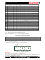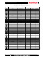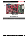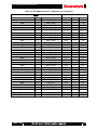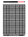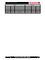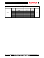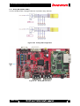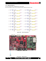
1
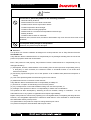
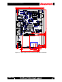
TB-7Z-ISDK Hardware User Manual TB-7Z-ISDK Hardware User Manual Rev.1.02 No reproduction or republication of part or the whole of the contents of this document is strictly prohibited. The company name and the product name described in this document is a trademark or a registered trademark of each company. Tokyo Electron Device Limited assumes no responsibility or liability for any damages, including, but not limited to, any special, incidental, or consequential damages arising out of any error in publication or the use of this document. The content of this document may be changed without prior notice. Rev.1.02 1 TB-7Z-ISDK Hardware User Manual Revision History: Version Date Rev.1.02 2015/10/15 Rev.1.02 Description Initial Release Publisher Kiguchi 2 TB-7Z-ISDK Hardware User Manual Table of Contents 1. 2. 3. 4. 5. Related Documents and Accessories ....................................................................................... 10 Overview .................................................................................................................................... 10 Feature ...................................................................................................................................... 10 3.1. Block Diagram ...........................................................................................................................11 3.2. External View of TB-7Z-ISDK ................................................................................................... 12 Board Specifications .................................................................................................................. 13 Description of Components ....................................................................................................... 15 5.1. Power supply ............................................................................................................................ 15 5.2. Power Input .............................................................................................................................. 15 5.3. Status Confirmation of the Board ............................................................................................. 16 5.4. Clock Configuration .................................................................................................................. 17 5.5. Spartan-6 (IC101) ..................................................................................................................... 17 5.5.1. 5.6. B2B Connector (CN801) .......................................................................................................... 19 5.6.1. 6. 7. Spartan-6 Bank Configuration .......................................................................................... 18 I/O Voltage Setting Jumper of USER_IOP/N (J101) ........................................................ 22 5.7. DVI TX (CN601) ....................................................................................................................... 23 5.8. CameraLink Base RX (CN701) ................................................................................................ 25 5.9. 10/100Mbps Ethernet (CN1101)............................................................................................... 28 5.10. USB 2.0 (CN804) .................................................................................................................. 30 5.11. CAN (CN902) ....................................................................................................................... 33 5.12. RS-232 (CN903) ................................................................................................................... 35 5.13. DDR2 SDRAM (IC501) ......................................................................................................... 38 5.14. QSPI Flash (IC201) .............................................................................................................. 42 5.15. DIP SW (SW1005) ................................................................................................................ 44 5.16. PUSH SW (SW0-3) .............................................................................................................. 46 5.17. Rotary SW (RSW0, RSW1) .................................................................................................. 48 5.18. LED0-15 (LED0-15) .............................................................................................................. 50 5.19. Pmod (J1003, J1004) ........................................................................................................... 52 5.20. ARM JTAG 20pin Header (JP802) ....................................................................................... 54 Generating a Spartan-6 Configuration File ............................................................................... 55 6.1. Settings when generating a configuration file (bit file) ............................................................. 55 6.2. Unused pin setting .................................................................................................................... 55 6.3. Generating a configuration file (mcs file).................................................................................. 56 6.4. Writing a Configuration File to the Flash Memory .................................................................... 62 Default Factory Settings ............................................................................................................ 67 Rev.1.02 3 TB-7Z-ISDK Hardware User Manual List of Figures Figure 3-1 TB-7Z-ISDK block diagram ...........................................................................................11 Figure 3-2 External view ............................................................................................................. 12 Figure 4-1 Board dimensions (inclusive of wastable substrate) ............................................ 14 Figure 5-1 Power sources ........................................................................................................... 15 Figure 5-2 Spartan-6 mounting diagram ................................................................................. 17 Figure 5-3 Spartan-6 Bank configuration .................................................................................. 18 Figure 5-4 TB-7Z-ISDN with TB-7Z-IAE .................................................................................... 19 Figure 5-5 I/O voltage setting pin ............................................................................................... 22 Figure 5-6 DVI TX configuration diagram .................................................................................. 23 Figure 5-7 DVI TX mounted ......................................................................................................... 23 Figure 5-8 CameraLink Base RX configuration diagram ......................................................... 25 Figure 5-9 CameraLink Base RX mounted ................................................................................ 26 Figure 5-10 10/100Mbps Ethernet mounted ................................................................................. 28 Figure 5-11 USB 2.0 configuration ............................................................................................. 30 Figure 5-12 USB 2.0 mounted ..................................................................................................... 31 Figure 5-13 CAN configuration ................................................................................................... 33 Figure 5-14 CAN mounted .......................................................................................................... 33 Figure 5-15 RS-232 configuration .............................................................................................. 35 Figure 5-16 RS-232 mounted ...................................................................................................... 36 Figure 5-17 DDR2 SDRAM configuration .................................................................................. 38 Figure 5-18 DDR2 SDRAM mounted .......................................................................................... 39 Figure 5-19 QSPI Flash configuration ....................................................................................... 42 Figure 5-20 QSPI Flash mounted .................................................................................................. 42 Figure 5-21 DIP SW configuration .............................................................................................. 44 Figure 5-22 DIP SW mounted ..................................................................................................... 44 Figure 5-23 PUSH SW configuration.......................................................................................... 46 Figure 5-24 PUSH SW mounted ................................................................................................. 46 Figure 5-25 Rotary SW configuration ........................................................................................ 48 Figure 5-26 Rotary SW mounted ................................................................................................ 48 Figure 5-27 LED configuration ................................................................................................... 50 Figure 5-28 LED mounted ........................................................................................................... 50 Figure 5-29 Pmod configuration ................................................................................................ 52 Figure 5-30 Pmod mounted ........................................................................................................ 52 Figure 5-31 ARM JTAG configuration ........................................................................................ 54 Figure 5-32 ARM JTAG mounted ................................................................................................ 54 Rev.1.02 4 TB-7Z-ISDK Hardware User Manual Figure 6-1 Process Properties window .......................................................................................... 55 Figure 6-2 Options setting when generating a bit file .................................................................... 55 Figure 6-3 Unused pin setting ....................................................................................................... 56 Figure 6-4 Generating a configuration file on ISE ......................................................................... 56 Figure 6-5 Warning message ........................................................................................................ 57 Figure 6-6 iMPACT window - 1 ...................................................................................................... 57 Figure 6-7 iMPACT window - 2 ...................................................................................................... 58 Figure 6-8 iMPACT window - 3 ...................................................................................................... 58 Figure 6-9 iMPACT window - 4 ...................................................................................................... 59 Figure 6-10 iMPACT window - 5 .................................................................................................... 59 Figure 6-11 iMPACT window - 6 .................................................................................................... 60 Figure 6-12 iMPACT window - 7 .................................................................................................... 60 Figure 6-13 iMPACT window - 8 .................................................................................................... 60 Figure 6-14 iMPACT window - 9 .................................................................................................... 61 Figure 6-15 iMPACT window - 10 .................................................................................................. 61 Figure 6-16 Onboard JTAG connector .......................................................................................... 62 Figure 6-17 Writing to a device - 1 ................................................................................................ 62 Figure 6-18 Writing to a device - 2 ................................................................................................ 63 Figure 6-19 Writing to a device - 3 ............................................................................................... 63 Figure 6-20 Writing to a device - 4 ............................................................................................... 64 Figure 6-21 Writing to a device - 5 ............................................................................................... 64 Figure 6-22 Writing to a device - 6 ............................................................................................... 65 Figure 6-23 Writing to a device - 7 ............................................................................................... 65 Figure 6-24 Writing to a device - 8 ............................................................................................... 66 Figure 6-25 Reconfiguration switch ............................................................................................... 66 Figure 6-26 Configuration status ................................................................................................... 66 Rev.1.02 5 TB-7Z-ISDK Hardware User Manual List of Tables Table 5-1 Status LED table .......................................................................................................... 16 Table 5-2 Clock input ..................................................................................................................... 17 Table 5-3 Spartan-6 Bank configuration table .......................................................................... 18 Table 5-4 B2B connector pin assignment table ........................................................................ 19 Table 5-5 I/O voltage of USER_IOP/ION ......................................................................................... 22 Table 5-6 DVI TX – Spartan-6 Pin Assignment ................................................................................ 24 Table 5-7 CameraLink PoCL setting ................................................................................................ 26 Table 5-8 CameraLink Base RX – Spartan-6 pin assignment ......................................................... 27 Table 5-9 10/100Mbps Ethernet – Spartan-6 pin assignment .......................................................... 29 Table 5-10 USB 2.0 – TB-7Z-IAE pin assignment ............................................................................ 32 Table 5-11 J802 USB bus power setting .......................................................................................... 32 Table 5-12 J803, J804, J805 USB mode setting .............................................................................. 32 Table 5-13 CAN – TB-7Z-IAE pin assignment.................................................................................. 34 Table 5-14 J903 CAN termination setting ........................................................................................ 34 Table 5-15 RS-232 – TB-7Z-IAE pin assignment ............................................................................. 36 Table 5-16 RS-232 – Spartan-6 pin assignment .............................................................................. 37 Table 5-17 J901 RXD signal connection setting .............................................................................. 37 Table 5-18 J902 TXD signal connection setting ............................................................................... 37 Table 5-19 DDR2 SDRAM pin assignment ...................................................................................... 40 Table 5-20 QSPI Flash pin assignment ............................................................................................ 43 Table 5-21 DIP SW pin assignment ................................................................................................. 45 Table 5-22 PUSH SW pin assignment ............................................................................................. 47 Table 5-23 Rotary SW pin assignment ............................................................................................. 49 Table 5-24 Rotary SW Output Signal Values ................................................................................... 49 Table 5-25 LED pin assignment ....................................................................................................... 51 Table 5-26 Pmod pin assignment ..................................................................................................... 53 Table 5-26 Pmod IO Voltage Settings .............................................................................................. 53 Table 5-28 ARM JTAG pin assignment ............................................................................................ 54 Table 7-1 Default factory settings ..................................................................................................... 67 Rev.1.02 6 TB-7Z-ISDK Hardware User Manual Introduction Thank you for purchasing the TB-7Z-ISDK board. Before using the product, be sure to carefully read this user manual and fully understand how to correctly use the product. First read through this manual and then always keep it handy. SAFETY PRECAUTIONS Be sure to observe these precautions Observe the precautions listed below to prevent injuries to you or other personnel or damage to property. Before using the product, read these safety precautions carefully to assure correct use. These precautions contain serious safety instructions that must be observed. After reading through this manual, be sure to always keep it handy. The following conventions are used to indicate the possibility of injury/damage and classify precautions if the product is handled incorrectly. Danger Indicates the high possibility of serious injury or death if the product is handled incorrectly. Indicates the possibility of serious injury or death if the product is handled Warning incorrectly. Indicates the possibility of injury or physical damage in connection with houses or Caution household goods if the product is handled incorrectly. The following graphical symbols are used to indicate and classify precautions in this manual. (Examples) Turn off the power switch. Do not disassemble the product. ! Rev.1.02 Do not attempt this. 7 TB-7Z-ISDK Hardware User Manual Warning In the event of a failure, disconnect the power supply. If the product is used as is, a fire or electric shock may occur. Disconnect the power supply immediately and contact our sales personnel for repair. If an unpleasant smell or smoking occurs, disconnect the power supply. If the product is used as is, a fire or electric shock may occur. immediately. Disconnect the power supply After verifying that no smoking is observed, contact our sales personnel for repair. Do not disassemble, repair or modify the product. Otherwise, a fire or electric shock may occur due to a short circuit or heat generation. For inspection, modification or repair, contact our sales personnel. ! Do not touch a cooling fan. As a cooling fan rotates in high speed, do not put your hand close to it. cause injury to persons. ! Otherwise, it may Never touch a rotating cooling fan. Do not place the product on unstable locations. Otherwise, it may drop or fall, resulting in injury to persons or failure. ! If the product is dropped or damaged, do not use it as is. ! Do not touch the product with a metallic object. ! Do not place the product in dusty or humid locations or where water may Otherwise, a fire or electric shock may occur. Otherwise, a fire or electric shock may occur. splash. Otherwise, a fire or electric shock may occur. ! ! Do not get the product wet or touch it with a wet hand. Otherwise, the product may break down or it may cause a fire, smoking or electric shock. Do not touch a connector on the product (gold-plated portion). Otherwise, the surface of a connector may be contaminated with sweat or skin oil, resulting in contact failure of a connector or it may cause a malfunction, fire or electric shock due to static electricity. Rev.1.02 8 TB-7Z-ISDK Hardware User Manual Caution Do not use or place the product in the following locations. ! Humid and dusty locations Airless locations such as closet or bookshelf Locations which receive oily smoke or steam Locations exposed to direct sunlight Locations close to heating equipment Closed inside of a car where the temperature becomes high Staticky locations Locations close to water or chemicals Otherwise, a fire, electric shock, accident or deformation may occur due to a short circuit or heat generation. ! Do not place heavy things on the product. Otherwise, the product may be damaged. ■ Disclaimer: This product is a function evaluation kit designed for mass production use of Tokyo Electron Device’s TB-7Z-IAE board. Tokyo Electron Device Limited assumes no responsibility for any damages resulting from the use of this product for purposes other than those stated. Even if the product is used properly, Tokyo Electron Device Limited assumes no responsibility for any damages caused by: (1) Earthquake, thunder, natural disaster or fire resulting from the use beyond our responsibility, acts by a third party or other accidents, the customer’s willful or accidental misuse or use under other abnormal conditions. (2) Secondary impact arising from use of this product or its unusable state (business interruption or others) (3) Use of this product against the instructions given in this manual. (4) Malfunctions due to connection to other devices. Tokyo Electron Device Limited assumes no responsibility or liability for: (1) Erasure or corruption of data arising from use of this product. (2) Any consequences or other abnormalities arising from use of this product, or (3) Damage of this product not due to our responsibility or failure due to modification This product has been developed by assuming its use for research, testing or evaluation. It is not authorized for use in any system or application that requires high reliability. Repair of this product is carried out by replacing it on a chargeable basis, not repairing the faulty devices. However, non-chargeable replacement is offered for initial failure if such notification is received within two weeks after delivery of the product. The specification of this product is subject to change without prior notice. The product is subject to discontinuation without prior notice. Rev.1.02 9 TB-7Z-ISDK Hardware User Manual 1. Related Documents and Accessories Related documents: All documents related to this board can be downloaded from our website. Board Fixtures: Industrial Grade SoM(System On Module) TB-7Z-IAE Board Foot Rubber foot: 9, Screw M3 L=6: 8, Spacer M3 L=10: 9 Jumper Socket : 6 Board Accessories: AC Adaptor AKIZUSHI DENSHI: LTE(GFP)451DA-1238 (equivalent): 1 Jumper Socket : 7 2. Overview The TB-7Z-ISDK board is an evaluation kit which is built on a dedicated Spartan-6 board incorporating the embedded module “TB-7Z-IAE” providing various interfaces for use of industrial network products. The TB-7Z-ISDK board is equipped with camera input and monitor output interface including serial interfaces for industrial products, which can be used for functional evaluation of a wide variety of industrial products from IO control device to inspection system. 3. Feature Evaluation kit of the embedded module “TB-7Z-IAE” for industrial network products Built on a dedicated Spartan-6 board to evaluate the functionality of the TB-7Z-IAE Serial interfaces such as RS232C and CAN which are used for industrial products With CameraLink Base RX image capture and DVI TX monitor output function, an image processing system fully utilizing the TB-7Z-IAE performance is configurable. 128MByte DDR2 SDRAM that allows storage of image frame buffers and large volumes of data Peripherals for debugging such as LED, PUSH SW, DIP SW and Rotary SW Rev.1.02 10 TB-7Z-ISDK Hardware User Manual 3.1. Block Diagram Figure 3-1 shows the TB-7Z-ISDK block diagram. TB-7Z-ISDK is a kit combining the “TB-7Z-IAE” and the dedicated Spartan-6 board. Figure 3-1 Rev.1.02 TB-7Z-ISDK block diagram 11 TB-7Z-ISDK Hardware User Manual 3.2. External View of TB-7Z-ISDK Figure 3-2 shows the external view of the TB-7Z-ISDK. Figure 3-2 Rev.1.02 External view 12 TB-7Z-ISDK Hardware User Manual 4. Board Specifications Figure 4-1 shows the specifications of the dedicated Spartan-6 board. External dimensions: 185.00mm (W), 110.00mm (H) Number of layers: 8 layers Board thickness: 1.6mm Material: FR-4 FPGA XC6SLX45-2FGG484C Memory 128MByte DDR2 SDRAM Component 64Mbit Quad SPI (QSPI) Flash CAMERA LINK 3M 12226-5150-00PL B2B Connector SAMTEC ERF8-060-05.0-L-DV-K-TR Ethernet MICREL KSZ9031MNXIA RJ-45 BEL L834-1G1T-32 USB Connector MOLEX 67803-8020 DVI TI TFP410PAP DVI Transmitter: RS-232C TI TRS3243EIDBR CAN Bus TI SN65HVD233D Pmod Connector TI TXS0108EPWR Clock 74.25MHz, 25MHz OSC Rev.1.02 13 TB-7Z-ISDK Hardware User Manual Figure 4-1 Rev.1.02 Board dimensions (inclusive of wastable substrate) 14 TB-7Z-ISDK Hardware User Manual 5. Description of Components 5.1. Power supply Figure 5-1 shows the power sources. CN1 12V TPS54527 5V TPS54327 1.2V Spartan-6 (VCCINT) TPS54227 1.8V Spartan-6 (VCCO), DDR2 TPS54227 3.3V Spartan-6 (VCCO), QSPI, DVI, RS232C, CAN, PMOD, TB-7Z-IAE (VCCO) TPS54227 2.5V Spartan-6 (VCCO), CameraLink, TB-7Z-IAE (VCCO) 12V CameraLink Figure 5-1 5.2. TB-7Z-IAE, DVI, USB, PMOD Power sources Power Input Connect the attached AC adaptor (12V) to CN1. When the switch (SW1) is set to ON, power is turned. Rev.1.02 15 TB-7Z-ISDK Hardware User Manual 5.3. Status Confirmation of the Board The power status of the board can be checked by visually observing the associated LED indicator. The board also provides a status LED indicator which shows the completion of Spartan-6 configuration after power is up. Table 5-1 Status LED table Onboard silk Description LED1 Yellow. 12V power OK LED201 Yellow. Completion of Zynq PL configuration Rev.1.02 16 TB-7Z-ISDK Hardware User Manual 5.4. Clock Configuration The board has the following clock sources. They are connected to the Spartan-6. Table 5-2 Clock input Connection Signal Name IF Spartan-6 PIN Remarks IC202 (74.25MHz) CLK_74_25M LVCMOS33 AA12 DVI clock IC204 (25MHz) CLK_25_000M LVCMOS33 Y13 Ethernet clock Spartan-6 (IC101) The TB-7Z-ISDK board is equipped with Spartan-6 XC6SLX45 for multiple uses of TB-7Z-IAE’s IOs. Figure Rev.1.02 5-2 Spartan-6 mounting diagram 17 TB-7Z-ISDK Hardware User Manual 5.5.1. Spartan-6 Bank Configuration Each IO Bank of Spartan-6 is connected to various interfaces and memory devices other than TB-7Z-IAE. Figure 5-5 and Table 5-3 show the Spartan-6 Banks and the devices to which they are connected. Figure 5-3 Spartan-6 Bank configuration Bank Connect to Level 0 CameraLink, D-SUB9(UART) 2.5V 1 TB-7Z-IAE:USER_IOP/N, PMOD, RSW 2.5V or 3.3V 2 DVI, QSPI Flash, Ethernet, TB-7Z-IAE:USER_GIO 3.3V 3 DDR2 SDRAM, LED, PSW, 1.8V Table 5-3 Rev.1.02 Spartan-6 Bank configuration table 18 TB-7Z-ISDK Hardware User Manual 5.6. B2B Connector (CN801) The TB-7Z-ISDN board provides one TB-7Z-IAE dedicated connector (B2B connector). At the time of shipment, the board comes with TB-7Z-IAE. Hot swapping is not allowed. TB-7Z-IAE’s Zynq PS MIO, Zynq PL IO, USB 2.0, ADC input, 5V power input and GND are included. Figure 5-4 TB-7Z-ISDN with TB-7Z-IAE Table 5-4 shows the pin assignment table associated with TB-7Z-IAE. In the table below, “Dir” means signal directions based on the Spartan-6 mounted board. Table 5-4 B2B connector pin assignment table Connect to Spartan-6 Description Signal Name DIR Pin LOC Bank Level - 1 DGND - - - - Ground 2 DGND - - - - Ground 3 USER_IOP00 I/O C19 1 *1 Spartan-6 Configurable IO (DIFF P) 4 USER_IOP01 I/O G16 1 *1 Spartan-6 Configurable IO (DIFF P) 5 USER_ION00 I/O B20 1 *1 Spartan-6 Configurable IO (DIFF N) 6 USER_ION01 I/O G17 1 *1 Spartan-6 Configurable IO (DIFF N) 7 DGND - - - - Ground 8 DGND - - - - Ground 9 USER_IOP02 I/O F16 1 *1 Spartan-6 Configurable IO (DIFF P) 10 USER_IOP03 I/O B21 1 *1 Spartan-6 Configurable IO (DIFF P) 11 USER_ION02 I/O F17 1 *1 Spartan-6 Configurable IO (DIFF N) 12 USER_ION03 I/O B22 1 *1 Spartan-6 Configurable IO (DIFF N) 13 DGND - - - Ground No. Rev.1.02 - 19 TB-7Z-ISDK Hardware User Manual Connect to Spartan-6 14 DGND - - 15 USER_IOP04 I/O A20 16 USER_IOP05 I/O 17 USER_ION04 18 - Ground 1 *1 Spartan-6 Configurable IO (DIFF P) K16 1 *1 Spartan-6 Configurable IO (DIFF P) I/O A21 1 *1 Spartan-6 Configurable IO (DIFF N) USER_ION05 I/O J16 1 *1 Spartan-6 Configurable IO (DIFF N) 19 DGND - - - - Ground 20 DGND - - - - Ground 21 USER_IOP06 I/O H16 1 *1 Spartan-6 Configurable IO (DIFF P) 22 USER_IOP07 I/O D19 1 *1 Spartan-6 Configurable IO (DIFF P) 23 USER_ION06 I/O H17 1 *1 Spartan-6 Configurable IO (DIFF N) 24 USER_ION07 I/O D20 1 *1 Spartan-6 Configurable IO (DIFF N) 25 DGND - - - - Ground 26 DGND - - - - Ground 27 USER_IOP08 I/O F18 1 *1 Spartan-6 Configurable IO (DIFF P) 28 USER_IOP09 I/O D21 1 *1 Spartan-6 Configurable IO (DIFF P) 29 USER_ION08 I/O F19 1 *1 Spartan-6 Configurable IO (DIFF N) 30 USER_ION09 I/O D22 1 *1 Spartan-6 Configurable IO (DIFF N) 31 DGND - - - - Ground 32 DGND - - - - Ground 33 USER_IOP10 I/O C20 1 *1 Spartan-6 Configurable IO (DIFF P) 34 USER_IOP11 I/O G19 1 *1 Spartan-6 Configurable IO (DIFF P) 35 USER_ION10 I/O C22 1 *1 Spartan-6 Configurable IO (DIFF N) 36 USER_ION11 I/O F20 1 *1 Spartan-6 Configurable IO (DIFF N) 37 DGND - - - - Ground 38 DGND - - - - Ground 39 USER_IOP12 I/O H19 1 *1 Spartan-6 Configurable IO (DIFF P) 40 USER_IOP13 I/O E20 1 *1 Spartan-6 Configurable IO (DIFF P) 41 USER_ION12 I/O H18 1 *1 Spartan-6 Configurable IO (DIFF N) 42 USER_ION13 I/O E22 1 *1 Spartan-6 Configurable IO (DIFF N) 43 DGND - - - - Ground 44 DGND - - - - Ground 45 USER_IOP14 I/O J17 1 *1 Spartan-6 Configurable IO (DIFF P) 46 USER_IOP15 I/O F21 1 *1 Spartan-6 Configurable IO (DIFF P) 47 USER_ION14 I/O K17 1 *1 Spartan-6 Configurable IO (DIFF N) 48 USER_ION15 I/O F22 1 *1 Spartan-6 Configurable IO (DIFF N) 49 DGND - - - - Ground 50 DGND - - - - Ground 51 USER_IOP16 I/O H20 1 *1 Spartan-6 Configurable IO (DIFF P) 52 USER_IOP17 I/O G20 1 *1 Spartan-6 Configurable IO (DIFF P) 53 USER_ION16 I/O J19 1 *1 Spartan-6 Configurable IO (DIFF N) 54 USER_ION17 I/O G22 1 *1 Spartan-6 Configurable IO (DIFF N) 55 DGND - - - - Ground 56 DGND - - - - Ground Rev.1.02 - Description 20 TB-7Z-ISDK Hardware User Manual Connect to Spartan-6 Description 57 USER_IOP18 I/O K20 1 *1 Spartan-6 Configurable IO (DIFF P) GCLK 58 USER_IOP19 I/O H21 1 *1 Spartan-6 Configurable IO (DIFF P) GCLK 59 USER_ION18 I/O K19 1 *1 Spartan-6 Configurable IO (DIFF N) GCLK 60 USER_ION19 I/O H22 1 *1 Spartan-6 Configurable IO (DIFF N) GCLK 61 DGND - - - - Ground 62 DGND - - - - Ground 63 USER_IOP20 I/O M20 1 *1 Spartan-6 Configurable IO (DIFF P) GCLK 64 USER_IOP21 I/O J20 1 *1 Spartan-6 Configurable IO (DIFF P) GCLK 65 USER_ION20 I/O L19 1 *1 Spartan-6 Configurable IO (DIFF N) GCLK 66 USER_ION21 I/O J22 1 *1 Spartan-6 Configurable IO (DIFF N) GCLK 67 DGND - - - - Ground 68 DGND - - - - Ground 69 USER_IOP22 I/O K21 1 *1 Spartan-6 Configurable IO (DIFF P) 70 USER_IOP23 I/O L20 1 *1 Spartan-6 Configurable IO (DIFF P) 71 USER_ION22 I/O K22 1 *1 Spartan-6 Configurable IO (DIFF N) 72 USER_ION23 I/O L22 1 *1 Spartan-6 Configurable IO (DIFF N) 73 DGND - - - - Ground 74 DGND - - - - Ground 75 USER_MIO22 I/O - - - Connect to JP802 (ARM JTAG) 76 USER_MIO23 I/O - - - Connect to JP802 (ARM JTAG) 77 USER_MIO24 I/O - - - Connect to JP802 (ARM JTAG) 78 USER_MIO25 I/O - - - Connect to JP802 (ARM JTAG) 79 USER_MIO26 I/O - - - Connect to JP801 (IOB PH) 80 USER_MIO27 I/O - - - Connect to JP801 (IOB PH) 81 USER_MIO46 I/O - - - Connect to IC904 (CAN) 82 USER_MIO47 I/O - - - Connect to IC904 (CAN) 83 USER_MIO48 I/O - - - Connect to J902 (UART) 84 USER_MIO49 I/O - - - Connect to J901 (UART) 85 USER_GIO0 I/O AB5 2 3.3V Zynq PL Configurable IO 86 USER_GIO1 I/O AA4 2 3.3V Zynq PL Configurable IO 87 USER_GIO2 I/O AB4 2 3.3V Zynq PL Configurable IO 88 USER_GIO3 I/O Y3 2 3.3V Zynq PL Configurable IO 89 USER_GIO4 I/O AB3 2 3.3V Zynq PL Configurable IO 90 USER_GIO5 I/O R9 2 3.3V Zynq PL Configurable IO 91 USER_GIO6 I/O R8 2 3.3V Zynq PL Configurable IO 92 USER_GIO7 I/O T7 2 3.3V Zynq PL Configurable IO 93 USER_GIO8 I/O R7 2 3.3V Zynq PL Configurable IO 94 USER_GIO9 I/O W4 2 3.3V Zynq PL Configurable IO 95 USER_GIO10 I/O Y4 2 3.3V Zynq PL Configurable IO 96 USER_GIO11 I/O U6 2 3.3V Zynq PL Configurable IO 97 DGND - - - - Ground 98 DGND - - - - Ground 99 PS_POR_B_MR O - - - Connect to SW801 (PSW) Rev.1.02 21 TB-7Z-ISDK Hardware User Manual Connect to Spartan-6 Description 100 USB_CPEN I - - - Connect to IC801 (USB) 101 PS_SRST O - - - Connect to JP802 (ARM JTAG) 102 USB_VBUS Power - - - Connect to CN804 (USB) 103 GND - - - - Ground 104 USB_ID O - - - Connect to CN804 (USB) 105 VP_0 O - - 106 GND - - - 107 VN_0 O - - 108 USB_DP IO - - - Connect to CN804 (USB) 109 GND - - - - Ground 110 USB_DM IO - - - Connect to CN804 (USB) 111 BATT Power - - - Connect to BATT801 112 GND - - - - Ground 113 +3.3VD Power - - - - 114 +5VD Power - - - Board Supply 115 +5VD Power - - - Board Supply 116 +5VD Power - - - Board Supply 117 +5VD Power - - - Board Supply 118 +5VD Power - - - Board Supply 119 +5VD Power - - - Board Supply 120 +5VD Power - - - Board Supply 5.6.1. Connect to JP801 (IOB PH) - Ground Connect to JP801 (IOB PH) I/O Voltage Setting Jumper of USER_IOP/N (J101) As for USER_IOP/N00 through 23, I/O voltage can be set to 3.3V or 2.5V. Table 5-5 I/O voltage of USER_IOP/ION VCCO J101 3.3V 1-2 2.5V 2-3 Figure 11-7 shows the jumper pins. The position of a triangular silk marking on the board indicates PIN1. Figure 5-5 I/O voltage setting pin IMPORTANT: JP101 setting must match the setting on the TB-7Z-IAE side. Before performing the setting, be sure to turn off the power switch of the TB-7Z-IAE and the user board, otherwise it may cause damage to the board. Rev.1.02 22 TB-7Z-ISDK Hardware User Manual 5.7. DVI TX (CN601) The TB-7Z-ISDK board is equipped with an image output DVI-D (Single Link) connector and a transmitter (TI’s TFP410 or equivalent). The board has been designed for operation at 148.5MHz. Image output of 1920x1080x24pixel@60p has been confirmed. Figure 5-6 DVI TX configuration diagram Figure 5-7 Rev.1.02 DVI TX mounted 23 TB-7Z-ISDK Hardware User Manual Table 5-6 DVI TX – Spartan-6 Pin Assignment Connect to Spartan-6 No. Name Signal Name Pin No. Bank Level 1 DATA0 DVI_B0 R16 2 3.3V 2 DATA1 DVI_B1 R15 2 3.3V 3 DATA2 DVI_B2 V17 2 3.3V 4 DATA3 DVI_B3 W17 2 3.3V 5 DATA4 DVI_B4 V15 2 3.3V 6 DATA5 DVI_B5 AA18 2 3.3V 7 DATA6 DVI_B6 AB18 2 3.3V 8 DATA7 DVI_B7 Y17 2 3.3V 9 DATA8 DVI_G0 AB17 2 3.3V 10 DATA9 DVI_G1 AA14 2 3.3V 11 DATA10 DVI_G2 AB14 2 3.3V 12 DATA11 DVI_G3 Y16 2 3.3V 13 DATA12 DVI_G4 W15 2 3.3V 14 DATA13 DVI_G5 V13 2 3.3V 15 DATA14 DVI_G6 W13 2 3.3V 16 DATA15 DVI_G7 AA16 2 3.3V 17 DATA16 DVI_R0 AB16 2 3.3V 18 DATA17 DVI_R1 W14 2 3.3V 19 DATA18 DVI_R2 Y14 2 3.3V 20 DATA19 DVI_R3 Y15 2 3.3V 21 DATA20 DVI_R4 AB15 2 3.3V 22 DATA21 DVI_R5 T12 2 3.3V 23 DATA22 DVI_R6 U12 2 3.3V 24 DATA23 DVI_R7 T14 2 3.3V 25 DKEN DVI_DKEN U17 2 3.3V 26 DE DVI_DE U16 2 3.3V 27 HSYNC DVI_HSYNC V19 2 3.3V 28 VSYNC DVI_VSYNC V18 2 3.3V 29 CTL3/A3/DK3 DVI_CTL1 T18 2 3.3V 30 CTL2/A2/DK2 DVI_CTL2 T17 2 3.3V 31 CTL1/A1/DK1 DVI_CTL3 Y19 2 3.3V 32 /PD DVI_PWRDN AB19 2 3.3V 33 MSEN/PO1 DVI_MSEN W18 2 3.3V 34 ISEL/RST DVI_ISEL Y18 2 3.3V 35 DSEL/SDA SDA T16 2 3.3V 36 BSEL/SCL SCL T15 2 3.3V Rev.1.02 24 TB-7Z-ISDK Hardware User Manual 5.8. CameraLink Base RX (CN701) The TB-7Z-ISDK is equipped with an image data input interface for CameraLink Base camera. The board can provide an internal 12V power supply voltage generation circuit by setting J701. So, the Power over Camera Link (PoCL) camera can also be supported. Important: Be sure to match the PoCL enable/disable setting (J701) of the TB-7Z-ISDK with that of a camera before connecting them. A Fuse (F701) is inserted but at worst, connected devices or the TB-7Z-ISDK board may be damaged. Figure 5-8 Rev.1.02 CameraLink Base RX configuration diagram 25 TB-7Z-ISDK Hardware User Manual Figure 5-9 CameraLink Base RX mounted Table 5-7 CameraLink PoCL setting Rev.1.02 CL Power J701 +12VD 1-2 OFF Open 26 TB-7Z-ISDK Hardware User Manual Table 5-8 CameraLink Base RX – Spartan-6 pin assignment Connect to Spartan-6 Name DIR Signal Name Pin LOC Bank Level CC4- I/O CC4N A7 0 2.5V CC3+ I/O CC3P B6 0 2.5V CC2- I/O CC2N C6 0 2.5V CC1+ I/O CC1P C5 0 2.5V SerTFG+ I/O CMR_SERTFGP B10 0 2.5V SerTC- I/O CMR_SERTCN C10 0 2.5V X3+ I/O CMR_X3P D7 0 2.5V Xclk+ I/O CMR_XCLKP B10 2 3.3V X2+ I/O CMR_X2P C9 0 2.5V X1+ I/O CMR_X1P D9 0 2.5V X0+ I/O CMR_X0P B8 0 2.5V CC4+ I/O CC4P C7 0 2.5V CC3- I/O CC3N A6 0 2.5V CC2+ I/O CC2P D6 0 2.5V CC1- I/O CC1N A5 0 2.5V SerTFG- I/O CMR_SERTFGN A10 0 2.5V SerTC+ I/O CMR_SERTCP D10 0 2.5V X3- I/O CMR_X3N D8 0 2.5V Xclk- I/O CMR_XCLKN A10 2 3.3V X2- I/O CMR_X2N A9 0 2.5V X1- I/O CMR_X1N C8 0 2.5V X0- I/O CMR_X0N A8 0 2.5V Rev.1.02 27 TB-7Z-ISDK Hardware User Manual 5.9. 10/100Mbps Ethernet (CN1101) The TB-7Z-ISDK board provides one each 10/100Mbps Ethernet PHY and RJ45 connector. They are connected to Spartan-6 and can be used as an additional TB-7Z-IAE communication port or an external communication interface for Spartan-6 itself. Figure 5-10 10/100Mbps Ethernet mounted Rev.1.02 28 TB-7Z-ISDK Hardware User Manual Table 5-9 10/100Mbps Ethernet – Spartan-6 pin assignment 接続先 Spartan-6 Name DIR Signal Name Pin LOC Bank Level LED2/PHYAD1 I GBE0_LED2 R11 2 3.3V TXD0 O GBE0_TXD[0] T11 2 3.3V TXD1 O GBE0_TXD[1] AA10 2 3.3V TXD2 O GBE0_TXD[2] AB10 2 3.3V TXD3 O GBE0_TXD[3] V11 2 3.3V TXD4 O GBE0_TXD[4] W11 2 3.3V TXD5 O GBE0_TXD[5] Y9 2 3.3V TXD6 O GBE0_TXD[6] AB9 2 3.3V TXD7 O GBE0_TXD[7] W10 2 3.3V TX_ER O GBE0_TXER Y10 2 3.3V GTX_CLK O GBE0_GTX_CLK AA8 2 3.3V TX_EN O GBE0_TXEN AB8 2 3.3V RXD7 I GBE0_RXD[7] W8 2 3.3V RXD6 I GBE0_RXD[6] V7 2 3.3V RXD5 I GBE0_RXD[5] W9 2 3.3V RXD4 I GBE0_RXD[4] Y8 2 3.3V RXD3 I GBE0_RXD[3] Y7 2 3.3V RXD2 I GBE0_RXD[2] AB7 2 3.3V RXD1 I GBE0_RXD[1] AA6 2 3.3V RXD0 I GBE0_RXD[0] AB6 2 3.3V RX_DV/CLK125_EN I GBE0_RXDV U9 2 3.3V RXER I GBE0_RXER V9 2 3.3V RESET_N O GBE0_PHYRST T8 2 3.3V CRS I GBE0_CRS U8 2 3.3V MDC O GBE_MDC T10 2 3.3V MDIO I/O GBE_MDIO U10 2 3.3V COL I GBE0_COL W6 2 3.3V INT_N/PME_N2 I GBE0_INTB Y6 2 3.3V XI O CLK_25M_GBE0 Y5 2 3.3V RX_CLK/PHYAD2 I GBE0_RXCLK W12 2 3.3V TX_CLK I GBE0_TXCLK Y12 2 3.3V Rev.1.02 29 TB-7Z-ISDK Hardware User Manual 5.10. USB 2.0 (CN804) The TB-7Z-ISDK board provides a USB 2.0 interface for connection to an external device. Since the connector (CN804) uses USB 2.0 Type-AB, it is needed to prepare an appropriate cable separately. The TB-7Z-ISDK board connects TB-7Z-IAE signals to the connector. Host/Device mode selection can be done on the board. Figure 5-11 Rev.1.02 USB 2.0 configuration 30 TB-7Z-ISDK Hardware User Manual Figure 5-12 Rev.1.02 USB 2.0 mounted 31 TB-7Z-ISDK Hardware User Manual Table 5-10 USB 2.0 – TB-7Z-IAE pin assignment TB-7Z-IAE Connect to Name Signal Name Pin No. Level VBUS USB_VBUS 102 5V DM USB_DM 110 DP USB_DP 108 ID USB_ID 104 EN USB_CPEN 100 3.3V Table 5-11 J802 USB bus power setting J802 Bus-Power short Enable open Disable Table 5-12 J803, J804, J805 USB mode setting Mode J803 J804 J805 HOST short short open OTG open short open DEVICE open open short Rev.1.02 32 TB-7Z-ISDK Hardware User Manual 5.11. CAN (CN902) The TB-7Z-ISDK board is equipped with a CAN interface for communication with an external device. An onboard D-SUB9 connector is used for this connection. The TB-7Z-ISDK board connects TB-7Z-IAE signals to the connector via the onboard CAN Transceiver. Figure 5-13 CAN configuration Figure 5-14 Rev.1.02 CAN mounted 33 TB-7Z-ISDK Hardware User Manual Table 5-13 CAN – TB-7Z-IAE pin assignment Connect to TB-7Z-IAE Name Signal Name B2B Pin No. D USER_MIO47 82 R USER_MIO46 81 LBK USER_GIO11 96 Level 3.3V Table 5-14 J903 CAN termination setting J903 CAN Termination 1-2 Enable open Disable Rev.1.02 34 TB-7Z-ISDK Hardware User Manual 5.12. RS-232 (CN903) The TB-7Z-ISDK board is equipped with an RS-232 interface for communication with an external device. Since the interface is configured as DTE, use a cross cable when connected to a PC or others (DTE). The connection destination device, Spartan-6 or TB-7Z-IAE, to which the RS-232 TXD/RXD signal is connected, can be selected using J901 and J902. As for Spartan-6, a control signal such as (RTS) is also connected. ROUT5 ROUT4 ROUT3 ROUT2 Rev.1.02 DIN3 DIN2 R9 R8 AA4 Y3 AB4 AB3 Figure 5-15 RS-232 configuration 35 TB-7Z-ISDK Hardware User Manual Figure 5-16 RS-232 mounted Table 5-15 RS-232 – TB-7Z-IAE pin assignment Connect to TB-7Z-IAE Name Signal Name B2B Pin No. DIN1 USER_MIO48 83 ROUT1 USER_MIO49 84 Rev.1.02 Level 3.3V 36 TB-7Z-ISDK Hardware User Manual Table 5-16 RS-232 – Spartan-6 pin assignment Connect to Spartan-6 Name DIR Signal Name Pin LOC Bank DIN1 O FPGA_UART_TX A11 0 ROUT1 I FPGA_UART_RX C11 0 DIN2 O TTL0RTS C13 0 DIN3 O TTL0DTR A13 0 ROUT2 I TTL0DSR D11 0 ROUT3 I TTL0DCD C12 0 ROUT4 I TTL0CTS B12 0 ROUT5 I TTL0RI A12 0 Level 2.5V Table 5-17 J901 RXD signal connection setting J901 Connect to 1-2 TB-7Z-IAE 2-3 Spartan-6 Table 5-18 J902 TXD signal connection setting J902 Connect to 1-2 TB-7Z-IAE 2-3 Spartan-6 Rev.1.02 37 TB-7Z-ISDK Hardware User Manual 5.13. DDR2 SDRAM (IC501) The TB-7Z-ISDK board is equipped with DDR2 SDRAM (Micron’s MT47H64M16HR-3:H or equivalent). It can be used for storage of user data including image frame buffer. Specification 1Gbit (8M x 16 x 8bank) Address configuration Bank=3bit Address=13bit (Row address=13bit / Column address=10bit) Data bus configuration Byte access with data strobe signal (DQS), data mask for each byte Data mask signal (DM) is controlled on a byte-by-byte basis. IC101 IC501 A0-13 BA0-2 ODT /CAS /RAS /WE CK /CLK /UDQS UDQS /LDQS LDQS UDM LDM DQ /CS DGND DDR2 SDRAM Spartan-6 Figure 5-17 Rev.1.02 DDR2 SDRAM configuration 38 TB-7Z-ISDK Hardware User Manual Figure 5-18 Rev.1.02 DDR2 SDRAM mounted 39 TB-7Z-ISDK Hardware User Manual Table 5-19 DDR2 SDRAM pin assignment DDR2 Spartan-6 Name DIR Signal Name Pin LOC Bank Level A0 O RAM_0_A0 H2 3 1.8V A1 O RAM_0_A1 H1 3 1.8V A2 O RAM_0_A2 H5 3 1.8V A3 O RAM_0_A3 K6 3 1.8V A4 O RAM_0_A4 F3 3 1.8V A5 O RAM_0_A5 K3 3 1.8V A6 O RAM_0_A6 J4 3 1.8V A7 O RAM_0_A7 H6 3 1.8V A8 O RAM_0_A8 E3 3 1.8V A9 O RAM_0_A9 E1 3 1.8V A10 O RAM_0_A10 G4 3 1.8V A11 O RAM_0_A11 C1 3 1.8V A12 O RAM_0_A12 D1 3 1.8V A13 O RAM_0_A13 G6 3 1.8V BA0 O RAM_0_BA0 G3 3 1.8V BA1 O RAM_0_BA1 G1 3 1.8V BA2 O RAM_0_BA2 F1 3 1.8V CK O RAM_0_CK+ H4 3 1.8V /CK O RAM_0_CK- H3 3 1.8V /RAS O RAM_0_RAS K5 3 1.8V /CAS O RAM_0_CAS K4 3 1.8V CKE O RAM_0_CKE D2 3 1.8V /WE O RAM_0_WE F2 3 1.8V ODT O RAM_0_ODT J6 3 1.8V DQ0 I/O RAM_0_DQ0 N3 3 1.8V DQ1 I/O RAM_0_DQ1 N1 3 1.8V DQ2 I/O RAM_0_DQ2 M2 3 1.8V DQ3 I/O RAM_0_DQ3 M1 3 1.8V DQ4 I/O RAM_0_DQ4 J3 3 1.8V DQ5 I/O RAM_0_DQ5 J1 3 1.8V DQ6 I/O RAM_0_DQ6 K2 3 1.8V DQ7 I/O RAM_0_DQ7 K1 3 1.8V DQ8 I/O RAM_0_DQ8 P2 3 1.8V DQ9 I/O RAM_0_DQ9 P1 3 1.8V DQ10 I/O RAM_0_DQ10 R3 3 1.8V DQ11 I/O RAM_0_DQ11 R1 3 1.8V DQ12 I/O RAM_0_DQ12 U3 3 1.8V DQ13 I/O RAM_0_DQ13 U1 3 1.8V DQ14 I/O RAM_0_DQ14 V2 3 1.8V DQ15 I/O RAM_0_DQ15 V1 3 1.8V Rev.1.02 40 TB-7Z-ISDK Hardware User Manual DDR2 Spartan-6 LDQS I/O RAM_0_DQS0+ L3 3 1.8V /LDQS I/O RAM_0_DQS0- L1 3 1.8V UDQS I/O RAM_0_DQS1+ T2 3 1.8V /UDQS I/O RAM_0_DQS1- T1 3 1.8V LDM O RAM_0_DM0 L4 3 1.8V UDM O RAM_0_DM1 M3 3 1.8V Rev.1.02 41 TB-7Z-ISDK Hardware User Manual 5.14. QSPI Flash (IC201) The TB-7Z-ISDK board is equipped with 64Mbit QSPI Flash (Spansion’s S25FL064P equivalent) which is connected to Spartan-6 for its configuration. For information about configuration, refer to Section 6 “Creating a Configuration File”. Figure 5-19 QSPI Flash configuration Figure 5-20 QSPI Flash mounted Rev.1.02 42 TB-7Z-ISDK Hardware User Manual Table 5-20 QSPI Flash pin assignment Connect to Spartan-6 Name DIR Signal Name Pin No. Bank CS# O QSPI_CS T5 2 SO/IO1 I/O QSPI_IO1 AA20 2 WP#/IO2 I/O QSPI_IO2 U14 2 SI/IO0 I/O QSPI_IO0 AB20 2 SCK O QSPI_CLK Y21 2 HOLD#/IO3 O QSPI_IO3 U13 2 Rev.1.02 Level 3.3V 43 TB-7Z-ISDK Hardware User Manual 5.15. DIP SW (SW1005) The TB-7Z-ISDK board is equipped with an 8-pin DIP SW. When the switch is turned on, the corresponding FPGA pin is driven “high”. to Spartan-6 Figure 5-21 DIP SW configuration Figure 5-22 Rev.1.02 DIP SW mounted 44 TB-7Z-ISDK Hardware User Manual Table 5-21 DIP SW pin assignment Connect to Name SW1005 Rev.1.02 Spartan-6 DIR Signal Name Pin LOC Bank I DSW0 B1 3 I DSW1 G7 3 I DSW2 F7 3 I DSW3 D3 3 I DSW4 C4 3 I DSW5 E5 3 I DSW6 E6 3 I DSW7 A2 3 Level 1.8V 45 TB-7Z-ISDK Hardware User Manual 5.16. PUSH SW (SW0-3) The TB-7Z-ISDK is equipped with four PushSWs. When the switch is depressed, the corresponding FPGA input pin is driven “low”. Figure 5-23 PUSH SW configuration Figure 5-24 Rev.1.02 PUSH SW mounted 46 TB-7Z-ISDK Hardware User Manual Table 5-22 PUSH SW pin assignment Connect to Spartan-6 Name DIR Signal Name Pin LOC Bank SW1001 I PSW0 M6 3 SW1002 I PSW1 L6 3 SW1003 I PSW2 P3 3 SW1004 I PSW3 N4 3 Rev.1.02 Level 1.8V 47 TB-7Z-ISDK Hardware User Manual 5.17. Rotary SW (RSW0, RSW1) The TB-7Z-ISDK board is equipped with two 16-position rotary switches. Figure 5-25 Rotary SW configuration Figure 5-26 Rev.1.02 Rotary SW mounted 48 TB-7Z-ISDK Hardware User Manual Table 5-23 Rotary SW pin assignment Connect to Name SW1006 SW1007 Spartan-6 DIR Signal Name Pin No. Bank I RSW1_0 L15 1 I RSW2_0 P19 1 I RSW4_0 P20 1 I RSW8_0 W20 1 I RSW1_1 W22 1 I RSW2_1 L17 1 I RSW4_1 K18 1 I RSW8_1 U19 1 Level 2.5V or 3.3V Table 5-24 Rotary SW Output Signal Values SW Value Signal Value SW Value Signal Value 0 RSW[8,4,2,1]_x = 4’b0000 8 RSW[8,4,2,1]_x = 4’b1000 1 RSW[8,4,2,1]_x = 4’b0001 9 RSW[8,4,2,1]_x = 4’b1001 2 RSW[8,4,2,1]_x = 4’b0010 A RSW[8,4,2,1]_x = 4’b1010 3 RSW[8,4,2,1]_x = 4’b0011 B RSW[8,4,2,1]_x = 4’b1011 4 RSW[8,4,2,1]_x = 4’b0100 C RSW[8,4,2,1]_x = 4’b1100 5 RSW[8,4,2,1]_x = 4’b0101 D RSW[8,4,2,1]_x = 4’b1101 6 RSW[8,4,2,1]_x = 4’b0110 E RSW[8,4,2,1]_x = 4’b1110 7 RSW[8,4,2,1]_x = 4’b0111 F RSW[8,4,2,1]_x = 4’b1111 Rev.1.02 49 TB-7Z-ISDK Hardware User Manual 5.18. LED0-15 (LED0-15) The TB-7Z-ISDK board is equipped with 16 user LEDs. Each LED will light up when the corresponding FPGA output pin is driven “High”. Figure 5-27 Figure 5-28 Rev.1.02 LED configuration LED mounted 50 TB-7Z-ISDK Hardware User Manual Table 5-25 LED pin assignment Connect to Spartan-6 Name DIR Signal Name Pin No. Bank LED1001 O LED0 W3 3 LED1002 O LED1 W1 3 LED1003 O LED2 P8 3 LED1004 O LED3 P7 3 LED1005 O LED4 P6 3 LED1006 O LED5 P5 3 LED1007 O LED6 T4 3 LED1008 O LED7 T3 3 LED1009 O LED8 U4 3 LED1010 O LED9 V3 3 LED1011 O LED10 N6 3 LED1012 O LED11 N7 3 LED1013 O LED12 M7 3 LED1014 O LED13 M8 3 LED1015 O LED14 R4 3 LED1016 O LED15 P4 3 Rev.1.02 Level 1.8V 51 TB-7Z-ISDK Hardware User Manual 5.19. Pmod (J1003, J1004) The TB-7Z-ISDK board is equipped with two Pmod connectors. It provides a way of expanding various functions by connecting Digilent-provided Pmod modules. DIGILENT Home Page Peripheral Modules http://www.digilentinc.com/index.cfm Figure 5-29 Figure 5-30 Rev.1.02 Pmod configuration Pmod mounted 52 TB-7Z-ISDK Hardware User Manual Table 5-26 Pmod pin assignment Connect to Name J1003 J1004 OE Spartan-6 DIR Signal Name Pin No. Bank Level I/O PMOD_0_JA0 M21 1 I/O PMOD_0_JA1 M22 1 I/O PMOD_0_JA2 N20 1 I/O PMOD_0_JA3 N22 1 I/O PMOD_0_JA4 P21 1 I/O PMOD_0_JA5 P22 1 I/O PMOD_0_JA6 R20 1 I/O PMOD_0_JA7 R22 1 2.5V I/O PMOD_1_JA0 T22 1 or I/O PMOD_1_JA1 U20 1 3.3V I/O PMOD_1_JA2 U22 1 I/O PMOD_1_JA3 V21 1 I/O PMOD_1_JA4 V22 1 I/O PMOD_1_JA5 M19 1 I/O PMOD_1_JA6 N19 1 I/O PMOD_1_JA7 M16 1 O PMOD_OE T21 1 Table 5-27 Pmod IO Voltage Settings J1001, J1002 Pmod Level 1-2 5.0V 2-3 3.3V IMPORTANT: 5.0V setting is a Pmod standard spec violation. Don't connect a Pmod module at the 5.0V setting. Rev.1.02 53 TB-7Z-ISDK Hardware User Manual 5.20. ARM JTAG 20pin Header (JP802) The TB-7Z-ISDK board is equipped with one JTAG connector for ARM debugging. The connector is directly connected to TB-7Z-IAE. It allows for connection of a third party debugger to the Zynq AP SoC APU. Figure 5-31 ARM JTAG configuration Figure 5-32 ARM JTAG mounted Table 5-28 ARM JTAG pin assignment Connect to TB-7Z-IAE Name Signal Name Pin No. TDI USER_MIO22 75 TCK USER_MIO25 78 TMS USER_MIO24 77 TDO USER_MIO23 76 Rev.1.02 Level 3.3V 54 TB-7Z-ISDK Hardware User Manual 6. Generating a Spartan-6 Configuration File 6.1. Settings when generating a configuration file (bit file) The tool version used in the following description is “ISE14.7”. Right clock Generate Programming File in the Processes window and select Process properties. A Process Properties window will show up. Figure 6-1 Process Properties window The TB-7X-ISDK is equipped with QSPI Flash Memory for configuration. So, set the bus width to ”4” in the Configuration Options setting when generating a bit file. Note: Make sure that Property display level is set to Advanced. Figure 6-2 6.2. Options setting when generating a bit file Unused pin setting In the Configuration Options setting, set the unused pin setting to Float as shown in Figure 6-4. Rev.1.02 55 TB-7Z-ISDK Hardware User Manual Figure 6-3 Unused pin setting 6.3. Generating a configuration file (mcs file) The following procedure describes how to generate a configuration file. Generate a configuration file for writing data to the Flash memory. 1. Double click Generate Target PROM/ACE File. Figure 6-4 Generating a configuration file on ISE 2. When the following Warning shows up, click OK. Rev.1.02 56 TB-7Z-ISDK Hardware User Manual Figure 6-5 Warning message 3. When iMPACT is started up, double click Create PROM File. Figure 6-6 Rev.1.02 iMPACT window - 1 57 TB-7Z-ISDK Hardware User Manual 4. Select SPI Flash-Configure Single FPGA and click the rightwards arrow. Figure 6-7 iMPACT window - 2 5. Select 64M in the Storage Device (bits) field and click Add Storage Device. Figure 6-8 iMPACT window - 3 6. After clicking the rightwards arrow, fill in the Output File Name and Output File Location fields (directories) and then click OK. Rev.1.02 58 TB-7Z-ISDK Hardware User Manual Figure 6-9 iMPACT window - 4 Figure 6-10 iMPACT window - 5 7. Click OK. Rev.1.02 59 TB-7Z-ISDK Hardware User Manual 8. Choose a bit file for creating a configuration file. Figure 6-11 iMPACT window - 6 Figure 6-12 iMPACT window - 7 Figure 6-13 iMPACT window - 8 9. Click No. 10. Click OK. Rev.1.02 60 TB-7Z-ISDK Hardware User Manual 11. Double click Generate File. Figure 6-14 iMPACT window - 9 12. When the configuration file is created successfully, a Generate Succeeded message will be displayed. Figure 6-15 Rev.1.02 iMPACT window - 10 61 TB-7Z-ISDK Hardware User Manual 6.4. Writing a Configuration File to the Flash Memory Connect a Platform USB cable to the JTAG connector (CN401) as shown in Figure 6-17. onboard power supply. Turn on the Then run iMPACT and write a target configuration file to the Flash in accordance with the following procedure. Figure 6-16 1. Onboard JTAG connector Double click DoBoundary Scan. Then click Initialize Chain (indicated by an arrow). Figure 6-17 Rev.1.02 Writing to a device - 1 62 TB-7Z-ISDK Hardware User Manual 2. When a window to set bit and jed file options appears, cancel it. Select FPGA and then right click and select Add SPI/BPI Flash…. Figure 6-18 Writing to a device - 2 3. Choose a target configuration file (xxx.mcs) which is written to the Flash memory. Figure 6-19 Rev.1.02 Writing to a device - 3 63 TB-7Z-ISDK Hardware User Manual 4. Select the onboard Flash memory S25FL064P, set Data Width to 4, and click OK. Figure 6-20 Writing to a device - 4 5. Double click Program in the iMPACT Processes window. Figure 6-21 Rev.1.02 Writing to a device - 5 64 TB-7Z-ISDK Hardware User Manual 6. Click OK. Figure 6-22 Writing to a device - 6 7. The write operation will start. Figure 6-23 Rev.1.02 Writing to a device - 7 65 TB-7Z-ISDK Hardware User Manual 8. When the write operation is successfully completed, a Program Succeeded message will show up. Figure 6-24 Writing to a device - 8 9. The data written to the Flash memory is sent to the FPGA using QSPI for configuration. The configuration can be started by turning the onboard power supply on or by pressing the Reconfiguration Switch (SW201) as shown in Figure 6-26. Figure 6-25 Reconfiguration switch 10. The status of the FPGA configuration can be monitored by observing the LED201 shown in Figure 6-27. LED201 (yellow): Configuration completed successfully Figure 6-26 Configuration status Rev.1.02 66 TB-7Z-ISDK Hardware User Manual 7. Default Factory Settings Table 7-1 shows the TB-7Z-ISDK default factory settings. Observe the switches shown in Figure 7-1. Table 7-1 Default factory settings No. Jumper No. Default Setting Note 1 J101 2-3 2.5V 2 J701 1-2 12V 3 J802 open 4 J803 open 5 J804 open 6 J805 short 7 J806 open NC 8 J901 1-2 UART RXD = TB-7Z-IAE 9 J902 1-2 UART TXD = TB-7Z-IAE 10 J903 short CAN Termination Enable 11 J1001 2-3 Pmod 3.3V 12 J1002 2-3 Pmod 3.3V USB Device Mode No. DIP SW Default Setting Note 1 SW1005 all OFF DIP SW 2 SW1006 0 Rotary SW 3 SW1007 0 Rotary SW Rev.1.02 67 TB-7Z-ISDK Hardware User Manual inrevium http://solutions.inrevium.com/ HEAD Quarter: Yokohama East Square, 1-4 Kinko-cho, Kanagawa-ku, Yokohama City, Kanagawa, Japan 221-0056 TEL: +81-45-443-4016 FAX: +81-45-443-4058 Contact: http://solutions.inrevium.com/contact/index.html Rev.1.02 68