1
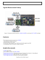
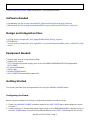
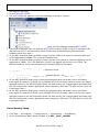
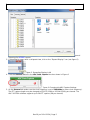
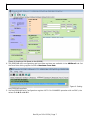
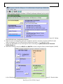
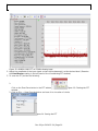
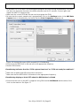
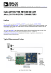
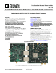
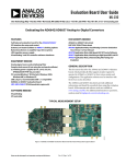
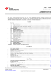
One Technology Way · P.O. Box 9106 · Norwood, MA 02062-9106 · Tel: 781.329.4700 · Fax: 781.461.3113 · www.analog.com
EVALUATING THE AD9680
ANALOG-TO-DIGITAL CONVERTER
Preface
This user guide describes the AD9680 evaluation board AD9680-1000EBZ which provides all of the
support circuitry required to operate the ADC in its various modes and configurations. The application
software used to interface with the devices is also described.
The AD9680 data sheet provides additional information and should be consulted when using the
evaluation board. All documents and software tools are available at www.analog.com/hsadcevalboard.
For additional information or questions, send an email to [email protected].
AD9680-1000EBZ
Figure 1. AD9680-1000EBZ Evaluation Board
Rev 18 Jun 2014 12:34 | Page 1
Typical Measurement Setup
Figure 2. Evaluation Board Connection—AD9680-1000EBZ (on Left) and ADS7-V1EBZ (on Right)
Features
●
●
●
●
●
Full featured evaluation board for the AD9680
SPI interface for setup and control
Wide band Balun driven input
No external supply needed. Uses 12V-1A and 3.3V-3A supplies from FMC
VisualAnalog® and SPI controller software interfaces
Helpful Documents
●
●
●
●
●
AD9680 Data Sheet
ADS7-V1EBZ evaluation kit (ADS7-V1EBZ)
AN-905 Application Note, VisualAnalog Converter Evaluation Tool Version 1.0 User Manual
AN-878 Application Note, High Speed ADC SPI Control Software
ADI SPI Application Note ADI Serial Control Interface Standard
Rev 18 Jun 2014 12:34 | Page 2
●
AN-835 Application Note, Understanding ADC Testing and Evaluation
Software Needed
●
●
VisualAnalog ftp://ftp.analog.com/pub/HSSP_SW/VisualAnalog/VisualAnalog_Setup.exe
SPIController ftp://ftp.analog.com/pub/adispi/A2DComponents/Install/SPIController_Setup.exe
Design and Integration Files
●
●
ftp://ftp.analog.com/pub/HSC_ADC_Apps/AD9680CE04B_Design_Support/
FPGA BIN file
ftp://ftp.analog.com/pub/HSC_ADC_Apps/ADs7-V1_packet/Firmware/ad9680_ads7v1_09242013_0949
am.bin
Equipment Needed
●
●
●
●
●
●
●
Analog signal source and antialiasing filter
Sample clock source
12V, 6.5A switching power supply (such as the SL POWER CENB1080A1251F01 supplied with
ADS7-V1EBZ)
PC running Windows®
USB 2.0 port
AD9680-1000EBZ board
ADS7-V1EBZ FPGA-based data capture kit
Getting Started
This section provides quick start procedures for using the AD9680-1000EBZ board.
Configuring the Board
Before using the software for testing, configure the evaluation board as follows:
1. Connect the AD9680-1000EBZ evaluation board to the ADS7-V1EBZ data capture board, as shown
in Figure 2.
2. Connect one 12V, 6.5A switching power supply (such as the CENB1080A1251F01 supplied) to P4 on
the ADS7-V1EBZ board. Connect the Standard-B USB port of the ADS7-V1EBZ board to the PC with
Rev 18 Jun 2014 12:34 | Page 3
the supplied USB cable.
3. Turn on the ADS7-V1EBZ.
4. The ADS7-V1EBZ will appear in the Device Manager as shown in Figure 3.
Figure 3. Device Manager showing ADS7-V1EBZ
5. If the Device Manager does not show the ADS7-V1EBZ listed as shown in Figure 2, unplug all USB
devices from the PC, uninstall and re-install SPIController and VisualAnalog and restart the
hardware setup from step 1.
6. On the ADC evaluation board, provide a clean, low jitter 1GHz clock source to connector J801 and
set the amplitude to 14dBm. This is the ADC Sample Clock.
7. On the ADC evaluation board, provide a clean, low jitter clock source to connector J804 and set the
amplitude to 10dBm. This is the Reference Clock for the gigabit transceivers in the FPGA. The
REFCLK frequency can be calculated using the following empirical formulae:
bps/lane, where
(Default Nprime = 16)
8. On the ADC evaluation board, use a clean signal generator with low phase noise to provide an
input signal for channel A to P200. Use a shielded, RG-58, 50 Ω coaxial cable to connect the signal
generator output to the ADC Evaluation Board. For best results, use a narrow-band, band-pass filter
with 50 Ω terminations and an appropriate center frequency. (ADI uses TTE, Allen Avionics, and K &
L band-pass filters.)
9. On the ADC evaluation board, use a clean signal generator with low phase noise to provide an
input signal for channel B to P202. Use a shielded, RG-58, 50 Ω coaxial cable to connect the signal
generator output to the ADC Evaluation Board. For best results, use a narrow-band, band-pass filter
with 50 Ω terminations and an appropriate center frequency. (ADI uses TTE, Allen Avionics, and K &
L band-pass filters.)
Visual Analog Setup
1. Click Start
All Programs
Analog Devices
VisualAnalog
VisualAnalog
2. On the VisualAnalog “New Canvas” window, click ADC Dual AD9680
Rev 18 Jun 2014 12:34 | Page 4
Figure 4.
Selecting the AD9680 canvas
3. If VisualAnalog opens with a collapsed view, click on the “Expand Display” icon (see figure 5)
Figure 5. Expanding Display in VA
4. Click the Settings button in the ADC Data Capture block as shown in Figure 6
Figure 6. Changing the ADC Capture Settings
5. On the General tab make sure the clock frequency is set to 1000MHz (or other clock frequency).
The FFT capture length may be changed to 131072 (128k) or 262144 (256k) per channel. The
ADs7-V1 FPGA software supports up to 2M FFT capture (1M per channel)
Rev 18 Jun 2014 12:34 | Page 5
Figure 7. Setting the clock frequency and Capture length
6. Click on the Capture Board tab and browse to the ad9680_ads7v1_09242013_0949am.bin file.
Click the Program button. The FPGA_DONE LED should illuminate on the ADS7-V1 board
indicating that the FPGA has been correctly programmed. The bin file is available at the ftp site
ftp://ftp.analog.com/pub/HSC_ADC_Apps/ADs7-V1_packet/Firmware/ad9680_ads7v1_09242013_094
9am.bin
7. On the Device tab. Make sure that Enable Alternate REFCLK option is unchecked.
8. Click OK
SPIController Setup
1. Click Start
All Programs
Analog Devices
SPIController
SPIController
2. Select the AD9680_14Bit_1.25GSspiR03.cfg if prompted.
3. In the Global tab, under the Generic Read/Write section, write 0x81 to register 0x000. This
issues a Soft reset for the DUT.
Rev 18 Jun 2014 12:34 | Page 6
Figure 8. Sending a Soft Reset to the AD9680
4. The JESD204B quick configuration and Lane Rate registers are available in the ADCBase3 tab. Set
the Lane Rate setting register 0x56E to Maximum Lane Rate
Figure 9. Setting
the JESD204B Lane Rate
5. Set the JESD204B Quick Configuration register 0x570. For 1000MSPS operation with no DDCs, the
values for L.M.F are 4.2.1
Rev 18 Jun 2014 12:34 | Page 7
Figure 10. Setting
the JESD204B Quick Configuration Register
6. After the quick configuration setting is completed, the PLL Lock Detect register 0x56F will read
0x80 to denote a lock. The SPIController interface will show a “1” to denote a lock.
7. Toggle the JESD204B link by checking and then unchecking the JESD204B Serial Transmit
Power Down box
8. Individual Channel control for ADC A and ADC B are done using the Device Index Register (0x008)
in the Global tab.
Figure 11. Device Index
Rev 18 Jun 2014 12:34 | Page 8
for ADC Channel A and Channel B
9. Under ADC A and ADC B tabs the options for Channel A and B are listed. Default settings have
been programmed to ensure optimal performance for the input bandwidth and sample rate. Only
the following options need to be operated with:
1. Chip Configuration Register (2): This option allows the channel to be powered on
2. Buffer Current Setting (18): This option allows the buffer current to change to enable better
harmonic performance at different frequencies. At high analog input frequencies, the buffer
current may need to be increased to optimize harmonic distortion performance (HD2, HD3).
Keep in mind that at high frequencies, the performance is also jitter limited. So increasing the
buffer currents may lead to diminishing returns with higher power consumption. Refer to the
datasheet to understand the relationship between IAVDD3 and Buffer Current Setting.
3. Analog Input Differential Termination (16): This sets the input termination. Recommended
settings are 500, 200, 100, 50 ohms. At lower termination settings, the harmonic distortion
performance may show improvement, but the analog input signal amplitude will be reduced.
4. Input Full Scale Range (25): At high input frequencies, in order to preserve the linearity of the
input buffer, it may be beneficial to reduce the input full-scale range in order to get more
harmonic distortion performance. This in turn may negatively affect the SNR of the ADC.
Obtaining an FFT
1. Click the Run button in VisualAnalog , you should see the captured data similar to the plot shown in
Figure 12.
Rev 18 Jun 2014 12:34 | Page 9
Figure 12. AD9680-1000 FFT at 170MHz Analog Input
2. Adjust the amplitude of the input signal so that the fundamental is at the desired level. (Examine
the Fund Power reading in the left panel of the VisualAnalog FFT window.)
3. To save the FFT plot do the following
1.
Click on the Float Form button in the FFT window
Figure 13. Floating the FFT
window
2. Click on File
Save Form As button and save it to a location of choice
Figure 14. Saving the FFT
Rev 18 Jun 2014 12:34 | Page 10
Troubleshooting Tips
FFT plot appears abnormal
●
●
●
If you see a normal noise floor when you disconnect the signal generator from the analog input, be
sure you are not overdriving the ADC. Reduce input level if necessary.
In VisualAnalog, Click on the Settings button in the Input Formatter block. Check that Number
Format is set to the correct encoding (twos compliment by default). Repeat for the other channel.
Issue a Data Path Soft Reset through SPIController Global tab as shown in Figure 15
Figure 15. Issuing a data path soft reset
through SPIController
The FFT plot appears normal, but performance is poor.
●
●
●
●
Make sure you are using the appropriate band-pass filter on the analog input.
Make sure the signal generators for the clock and the analog input are clean (low phase noise).
If you are using non-coherent sampling, change the analog input frequency slightly, or use coherent
frequencies.
Make sure the SPI config file matches the product being evaluated.
The FFT window remains blank after the Run button is clicked
●
●
Make sure the evaluation board is securely connected to the ADS7-V1.
Make sure the FPGA has been programmed by verifying that the Config DONE LED is illuminated
Rev 18 Jun 2014 12:34 | Page 11
●
●
●
●
on the ADS7-V1. If this LED is not illuminated reprogram the FPGA through VisualAnalog. If the LED
still does not illuminate disconnect the USB and power cord for 15 seconds. Connect again and
repeat the ADS7-V1 setup process.
Make sure the correct FPGA bin file was used to program the FPGA.
Be sure that the correct sample rate is programmed. Click on the Settings button in the ADC Data
Capture block in VisualAnalog, and verify that the Clock Frequency is properly set.
Figure 16. Setting the correct clock frequeency in VisualAnalog
Ensure that the REFCLOCK is ON and set to the appropriate frequency.
Restart SPIController.
VisualAnalog indicates that the “FIFO capture timed out” or “FIFO not ready for read back”
●
●
Make sure all power and USB connections are secure.
Make sure that the REFCLOCK is ON and set to the appropriate frequency.
VisualAnalog displays a blank FFT when the RUN button is clicked
●
Ensure that the clock to the ADC is supplied. Using SPIController ADCBase0 tab the status of the
clock can be read out. See figure 17.
Rev 18 Jun 2014 12:34 | Page 12
●
Figure 17. Clock
Detection Status Register
Ensure that the ADC's PLL is locked by checking the status of the PLL lock detect register 0x56F.
This can be done using SPIController.
© Analog Devices, Inc. All rights reserved. Trademarks and
registered trademarks are the property of their respective owners.
Rev 18 Jun 2014 12:34 | Page 13
www.analog.com