1
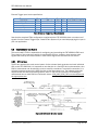
FSF-AD8200A
8-Channel, 185MSPS JESD204B ADC FMC
User Manual
January, 2014
Version 1.0
Fidus Systems Inc.
35 Fitzgerald Road, Suite 400
Ottawa, ON K2H 1E6
CANADA
Tel: (613) 828-0063
Fax: (613) 828-3113
Fidus Systems Inc. is at the forefront of technology innovation and for this reason, reserves the right to alter, without notice, the specification, design or
conditions of supply of any product or service. Information provided by Fidus Systems is believed to be accurate and reliable. However, no responsibility is
assumed by Fidus Systems Inc. for its use, nor any infringements of patents or other rights of third parties, which may result from its use. No license is granted
by implication or otherwise under any patent or patent rights of Fidus Systems Inc.
© 2014 Fidus Systems Inc. All Rights Reserved. Fidus’ name, Fidus logo, and “FMCs by Fidus” brand, are trademarks of Fidus Systems Inc. Other registered
and unregistered trademarks are the property of their respective owners. Information is subject to change without notice.
FSF-AD8200A User Manual
Revision History
Revision
0.1
0.2
0.3
Author
JLM
JLM
EJD
Release Date
06-18-2013
12-12-2013
12.19.2013
1.0
ST
01-03-2014
Fidus Systems Inc. – FMCs by Fidus
Description of Change
Draft
Updates
Updated section 4, to add info on Command Interface, Scripts,
and refer to the Getting Started Guide, and Command
Interface Guide.
Update. Release.
Page i of ii
FSF-AD8200A User Manual
Table of Contents
1. SAFETY INFORMATION AND PRODUCT AND COMPLIANCE LIMITATIONS ...................................................... 1 2. GENERAL OVERVIEW ...................................................................................................................................... 2 3. GLOSSARY....................................................................................................................................................... 4 4. REFERENCE DOCUMENTS .............................................................................................................................. 4 5. DETAILED SPECIFICATIONS ............................................................................................................................ 5 5.1 PERFORMANCE ............................................................................................................................................. 5 5.1.1 Input Frequency Response.................................................................................................................. 5 5.1.2 SNR, SFDR, and THD Plots .................................................................................................................. 7 5.1.3 Adjacent Channel Coupling ................................................................................................................. 8 5.1.4 Intermodulation ................................................................................................................................. 11 6. INTERFACES .................................................................................................................................................. 13 6.1 FMC INTERFACE: PIN SUPPORT AND OTHER REQUIREMENTS.............................................................................. 13 6.1.1 FSF-AD8200A HPC FMC pin assignment and definition ................................................................. 14 6.1.2 FMC Voltage and Current requirements ........................................................................................... 16 6.1.3 Multi-Gigabit Serial Communications Lines ..................................................................................... 16 6.2 ADC ANALOG INPUTS ................................................................................................................................... 17 6.3 EXTERNAL CLOCK INPUT ............................................................................................................................... 17 6.4 EXTERNAL TRIGGER INPUT ............................................................................................................................ 18 6.5 COMMUNICATION AND CONTROL .................................................................................................................... 19 6.5.1 SPI Interface ....................................................................................................................................... 19 6.5.1.1 6.5.1.2 6.5.2 7. Clock Generator ........................................................................................................................................20 Analog to Digital Converters .....................................................................................................................20 EEPROM ............................................................................................................................................. 21 ENVIRONMENTAL AND MECHANICAL ........................................................................................................... 22 7.1 ENVIRONMENT ............................................................................................................................................ 22 7.2 THERMAL CONSIDERATIONS .......................................................................................................................... 22 7.3 MECHANICAL .............................................................................................................................................. 23 7.3.1 Front Bezel (Faceplate) ..................................................................................................................... 23 7.3.2 Heat Sink ............................................................................................................................................ 24 8. DEMONSTRATION ......................................................................................................................................... 25 8.1 8.2 8.3 9. HARDWARE INSTALLATION............................................................................................................................. 25 SOFTWARE INSTALLATION ............................................................................................................................. 25 PERFORMING AN 8-CHANNEL CAPTURE .......................................................................................................... 27 ORDERING INFORMATION ............................................................................................................................ 28 10. WARRANTY ............................................................................................................................................... 28 11. APPENDIX A: ‘INIT’ SCRIPT CONTENTS ................................................................................................... 29 Fidus Systems Inc. – FMCs by Fidus
Page ii of ii
FSF-AD8200A User Manual
1. SAFETY INFORMATION AND PRODUCT AND COMPLIANCE LIMITATIONS
1. This product is designed for use and operation by an experienced electrical engineer or
someone with similar experience, knowledge, and capabilities.
2. This product is not an apparatus in accordance with the definition in EMC directive
(2004/108/EC), it is intended to be incorporated into an apparatus that is compliant to EMC
directive.
3.
To comply with the LVD directive (2006/95/EC), all the power sources for this card (12V,
3.3V, etc.) have to comply with LPS requirements as defined in IEC 60950-1.
4. This equipment must be disposed of and treated properly in compliance with WEEE directive
2012/19/EU, any product marked with this image
should not be disposed of in normal
household waste as products with electrical or electronic components can be recycled and
could also be harmful to the environment if sent to landfill.
5. This product is intended for incorporation into an apparatus that will carry the FCC 15
declaration.
Warning
Any unauthorized modification to this equipment may cause violation of the FCC or EMC rules
resulting in the revocation of the authorization to operate the equipment
Notes
This equipment must be disposed of and treated properly in compliance with WEEE directive
2012/19/EU
This equipment in ESD sensitive and must be handled using industry accepted methods to help
avoid damage from discharge events. This includes the wearing of grounding straps prior to and
while handling the circuit board.
Sensitive electronic device
Fidus Systems Inc. – FMCs by Fidus
Page 1 of 36
FSF-AD8200A User Manual
2. GENERAL OVERVIEW
The Fidus Systems FSF-AD8200A provides 8 channels of high performance analog capture in a VITA
57.1–2010 compatible, conduction cooled, single width FMC form factor.
Performance specifics include:
• Contains four IDT ADC1443D200 dual analog-to-digital converters
• JESD204B interface for low pin count, low noise, and deterministic latency
• Up to 185 MSPS conversion rate on each channel (default 180MSPS)
• 14-bit conversion on each channel
• Capable of sampling jitter below 100fsec RMS1
• Extremely low channel-to-channel crosstalk
• Input -3 dB bandwidth of >500MHz
The product has planned hardware compatibility with the following Xilinx® evaluation boards:
• Virtex VC707
• Virtex VC7092
• Kintex KC705 (capable of 4 lanes due to the MGT assignment)2
• Virtex ML605 (capable of 2 JESD204B cores of 4 lanes each)2
The VC707 package includes all necessary FPGA code/files to:
• Form a single link, 8-lane JESD204B connection
• Either load a default setting to all configuration registers or experiment with custom settings
• Capture ADC samples from each converter into FPGA block memory resources
• Access the captured ADC samples through ILA (formerly known as ChipScope®), where they
may then be exported for post processing
• Access all FSF-AD8200A registers through a command-line UART/terminal session
Figure 1 presents a detailed block diagram of the FSF-AD8200A functionality.
Integrated phase noise in a 12kHz–20MHz offset from a 180MHz clock frequency.
Although the existing hardware is theoretically compatible with these development boards, at the time of
writing, Fidus has only verified operation with the VC707 development kit.
1
2
Fidus Systems Inc. – FMCs by Fidus
Page 2 of 36
FSF-AD8200A User Manual
TERMINATION
NXP
74LVC1G125
SSMC
4K
TERMINATION
ADC1_LVDS_FRAME[PN] (1.8V)
SSMC
RF INPUT 1
BALUN
BALUN
ADC1A_CML[PN]
50
ADC1
TERMINATION
ADC1B_CML[PN]
SSMC
RF INPUT 2
BALUN
BALUN
BALUN
50
NXP
ADC1443D
TERMINATION
ADC2_LVDS_FRAME[PN] (1.8V)
SSMC
RF INPUT 3
VREF_A_M2C
(NOT CONNECTED)
BALUN
BALUN
50
+12V_FMC
+3V3_FMC
VADJ
ADC3_LVDS_FRAME[PN] (1.8V)
SSMC
RF INPUT 5
BALUN
([email protected] max)
NXP
ADC1443D
TERMINATION
BALUN
VIO_B_M2C
ADC2B_CML[PN]
SSMC
RF INPUT 4
BALUN
(NOT CONNECTED)
ADC2
TERMINATION
BALUN
VREF_B_M2C
ADC2A_CML[PN]
50
ADC3A_CML[PN]
50
ADC3
TERMINATION
FMC
CONNECTOR
ADC3B_CML[PN]
SSMC
RF INPUT 6
I2C
INTERMEDIATE
POWER
INDICATOR
EEPROM
(2K)
NXP
PCF85102C
EN_PWR
50
TERMINATION
BALUN
50
ADC_SCRAMBLER (1.8V)
50
CLKIN0
SYSREF
[LVDS]
SAMPLING
CLOCKS
[LVPECL]
CLK SPI BUS (3.3V)
SWITCHER_SYNQ[1:2] (VADJ)
LEVEL
TRANSLATE
CLKGEN_MAN_SYNC (3.3V)
CPOUT1
CLK SPI (VADJ)
CLKGEN_RESETn (VADJ)
CLKGEN_RESETn (3.3V)
OSCIN
LOW JITTER CLOCK
GENERATOR
CLKGEN_MAN_SYNC (VADJ)
74AVC1T45 / 74AVC8T245
OUT[6:4]
[LVDS]
OUT7
[LVDS]
+3V3_VCXO
TI
LP38798
SAMTEC
ASP-134488-01
M2C_FPGA_LVDS[2:1]_CLK[PN]
CTS / Valpey
R3306
120 MHz
+3V3_CLOCKING
TI
LP38798
LDO
50
LOOP
FILTER
LDO
ADC SPI (VADJ)
SWITCHER_SYNQ[1:2] (3.3V)
TERMINATION
VCXO
+4V
TI
TPS84250
ADC_SCRAMBLER_(VADJ)
ADC SPI BUS (1.8V)
NXP
ADC1443D
SSMC
CLK INPUT 1
[FRONT]
SWITCHER
SWITCHER_SYNQ1
ADC4B_CML[PN]
SSMC
RF INPUT 8
BALUN
+12V_FMC
ADC4A_CML[PN]
ADC4
TERMINATION
BALUN
POWER SYSTEM
ADC4_LVDS_FRAME[PN] (1.8V)
SSMC
RF INPUT 7
BALUN
PWR_GOOD
NXP
ADC1443D
GBTCLK[1:0]
BALUN
CLK1
BALUN
CLK0
TRIGGER INPUT
[LVTTL, 5V TOL]
SWITCHER
LDO
LDO
LDO
LDO
+2.5V
SWITCHER_SYNQ2
ADC4_LC_+1V8
ADC3_+1V8
ADC2_+1V8
ADC1_+1V8
M2C_FPGA_LVDS3_CLK[PN]
TI
TPS84250
M2C_FPGA_LVDS_SYSREF[PN]
TI
LMK04828
TI
TPS74801
PROJECT NAME
35 Fitzgerald Road
Ottawa, ON K2H 1E6
FSF-AD8200A
DRAWN
LOCK
TESTPOINT
ST / LM
DATE
6-15-13
TITLE
IDT / TI JESD204B
OCTAL ADC FMC, ROHS
CHECK
<CH INIT> <CH D>
DESIGN
SIZE
LQ / ST
6-15-13
<>
CODE IDENT.
N/A
DWG NO.
REV.
FMC_ADC_BD
2.0
ADDITIONAL INFO.
SCALE
RELEASE DATE
N/A
Figure 1: Detailed Block Diagram of the FSF-AD8200A
Fidus Systems Inc. – FMCs by Fidus
Page 3 of 36
11-15-2013
SHEET
1 OF 1
FSF-AD8200A User Manual
3. GLOSSARY
ADC
BW
C2M
CML
FMC
HPC
IMD
M2C
MGT
OFDM
SFDR
SNR
Analog-to-Digital Converter
Bandwidth
Carrier to Mezzanine (i.e. a signal output from carrier, input to FMC)
Current Mode Logic
FPGA Mezzanine Card
High Pin Count
Intermodulation
Mezzanine to Carrier (i.e. a signal output from the FMC, input to the carrier)
Multi-Gigabit Transceiver
Orthogonal Frequency Division Multiplexing
Spurious Free Dynamic Range
Signal to Noise Ratio
Xilinx®, Virtex®, and Vivado® are registered trademarks of Xilinx.
ChipScope™ is a trademark of Xilinx.
4. REFERENCE DOCUMENTS
ReferenceDocument
ANSI/VITA 57.1 FPGA
Mezzanine Card (FMC)
Standard – 2010. ISBN 1885731-49-3
IDT ADC1443D,
datasheet
TI LMK04828B,
datasheet
TI SN74AVC8T245
TI SN74AVC1T245
NXP PCF85102
CTS/VF R3306,
datasheet
FSF‐AD8200A
Function
Hyperlink
http://www.vita.com
ADC
Clock
Generator
Level shifter
Level shifter
EEPROM
120MHz VCXO
http://www.idt.com/document/dst/adc1443d-ser-datasheet
http://www.ti.com/lit/gpn/lmk04828
http://www.ti.com/lit/ds/symlink/sn74avc8t245.pdf
http://www.ti.com/lit/ds/symlink/sn74avc1t45.pdf
http://www.nxp.com/documents/data_sheet/PCF85102C_2.pdf
http://www.ctsvalpey.com/Collateral/Documents/EnglishUS/Products/FrequencyControl/Oscillators/VCXO/R3306.pdf
Table 1: Reference Documents
Fidus Systems Inc. – FMCs by Fidus
Page 4 of 36
FSF-AD8200A User Manual
5. DETAILED SPECIFICATIONS
5.1
Performance
The following sections present typical performance results, under the documented test conditions.
Test Conditions:
Ambient temperature: 25 ± 5°C
Description: Controlled laboratory environment
Test Platform: Xilinx VC707 development kit
Sample Rate: (178 + 4/7) MSPS
Parameter
Usable analog input BW
Min
Typ
1 to 700
Max
Unit
MHz
Fin = 4.989MHz
Conditions/Comments
S11 better than -7dB
@ -1.5dBFS
Nyquist Zone 1
SNR
SFDR
THD
Coupling (adjacent)
69
83.2
-79
-88.2
dBc
dBc
dBc
dB
Coupling (2nd adjacent)
-100.3
dB
SNR
SFDR
THD
Coupling (adjacent)
61.7
70.2
-74.8
-77.5
dBc
dBc
dBc
dB
Coupling (2nd adjacent)
-100.4
dB
Fin = 183.561MHz
averaged based on both
adjacent results
averaged based on both 2nd
adjacent results
@ -1.9dBFS
Nyquist Zone 3
averaged based on both
adjacent results
averaged based on both 2nd
adjacent results
Table 2: Typical Performance at 4.989 and 183.561MHz
Notes:
a) These results were captured without the heat sink and with additional applied air flow. The
heat sink was added for customer ease of adoption, and is not expected to affect the results
presented within this section.
5.1.1
Input Frequency Response
The ADC1443D converter claims a typical analog input bandwidth of 1GHz. On the FSF-AD8200A
both the low end and high end frequency response is limited by front-end components/filters. The
following plots describe the typical frequency performance of the inputs when swept.
Fidus Systems Inc. – FMCs by Fidus
Page 5 of 36
FSF-AD8200A User Manual
Figure 2: Overlay of typical Return Loss (S11) for all 8 Analog Input Channels (note log scale on x-axis)
The following plot describes the amplitude response and similarity of two analog inputs (Channel C
and Channel D)
Input C & D Amplitude Response (dB) vs Frequency (MHz)
0
0
100
200
300
400
500
600
700
800
900
1000
‐1
‐2
‐3
‐4
‐5
‐6
C
D
Figure 3: Typical Amplitude Response vs Frequency
Fidus Systems Inc. – FMCs by Fidus
Page 6 of 36
FSF-AD8200A User Manual
5.1.2
SNR, SFDR, and THD Plots
The following plots provide the basis for the numbers in the typical performance table above.
Figure 4: typical spectrum, Fin=4.989 MHz, Amp.=FS – 1.5dB (Nyquist Zone 1)
Figure 5: typical spectrum, Fin=183.561 MHz, Amp.=FS – 1.9dB (Nyquist Zone 3)
Fidus Systems Inc. – FMCs by Fidus
Page 7 of 36
FSF-AD8200A User Manual
5.1.3
Adjacent Channel Coupling
To limit coupling, the FSF-AD8200A has strategic ground plane design as well as individual front-end
shields. The following information describes the typical measured coupling between channels. When
referred to, adjacent and second adjacent are defined as:
Figure 6: Coupling terminology explanation
Input C coupling to B & D (dB) vs Frequency (MHz)
‐50
‐55
0
100
200
300
400
500
600
700
800
900
1000
‐60
‐65
‐70
‐75
‐80
‐85
‐90
‐95
B
D
Figure 7: Typical Channel – Channel Crosstalk (input C to adjacent channels)
Fidus Systems Inc. – FMCs by Fidus
Page 8 of 36
FSF-AD8200A User Manual
Input C coupling to A, E, F, G, H (dB) vs Frequency (MHz)
‐70
‐75
0
100
200
300
400
500
600
700
800
900
1000
‐80
‐85
‐90
‐95
‐100
‐105
‐110
A
E
F
G
H
Figure 8: Typical Channel – Channel Crosstalk (input C to non–adjacent channels)
Input D coupling to C & E (dB) vs Frequency (MHz)
‐50
‐55
0
100
200
300
400
500
600
700
800
900
1000
‐60
‐65
‐70
‐75
‐80
‐85
‐90
‐95
C
E
Figure 9: Typical Channel – Channel Crosstalk (input D to adjacent channels)
Fidus Systems Inc. – FMCs by Fidus
Page 9 of 36
FSF-AD8200A User Manual
Input D coupling to A, B, F, G, H (dB) vs Frequency (MHz)
‐70
‐75
0
100
200
300
400
500
600
700
800
900
1000
‐80
‐85
‐90
‐95
‐100
‐105
‐110
A
B
F
G
H
Figure 10: Typical Channel – Channel Crosstalk (input D to non–adjacent channels)
Fidus Systems Inc. – FMCs by Fidus
Page 10 of 36
FSF-AD8200A User Manual
5.1.4
Intermodulation
Figure 11: Two-tone IM3, F1=188.574MHz, F2=193.560MHz, amp=FS-7dB
Figure 12: Two-tone IM3, F1=188.574MHz, F2=193.560MHz, amp=FS-18dB
Fidus Systems Inc. – FMCs by Fidus
Page 11 of 36
FSF-AD8200A User Manual
Figure 13: Multi-tone, centered @ 160MHz, amp= -13.8dBFS RMS (Nyquist Zone 2)
Figure 14: OFDM, center=165MHz, BW=10MHz, amp= -14.4dBFS RMS (Nyquist Zone 2)
Fidus Systems Inc. – FMCs by Fidus
Page 12 of 36
FSF-AD8200A User Manual
6. INTERFACES
The FSF-AD8200A is comprised of both external and internal interfaces. The following interfaces are
discussed in this section.
•
•
•
•
•
6.1
FMC interface and pin-out
ADC analog inputs
External clock and trigger inputs
SPI interface to the clock generator
SPI interface to the ADC devices
FMC Interface: Pin support and other requirements
The FSF-AD8200A requires that the FMC carrier card contain a suitable HPC FMC connector. As the
FMC standard allows designers a certain amount of flexibility in pin selection and voltage support,
just because a carrier card as an HPC connector, it does not mean that it will be compatible with
every FMC with an HPC connector. Compatibility must be carefully assessed on a case-by-case basis.
The following sub-sections describe the support that the FSF-AD8200A requires from the carrier
card.
Fidus Systems Inc. – FMCs by Fidus
Page 13 of 36
FSF-AD8200A User Manual
6.1.1
FSF-AD8200A HPC FMC pin assignment and definition
FMC HPC Connector Details: Unshaded Cells are “No Connect” (NC) and list the VITA pin name.
Shaded Cells list the VITA pin name followed by FSF-AD8200A connection details.
K
J
1
VREF_B_M2C
GND
2
GND
CLK3_BIDIR_P
3
GND
CLK3_BIDIR_N
4
CLK2_BIDIR_P
GND
5
CLK2_BIDIR_N
GND
6
GND
HA03_P
7
HA02_P
HA03_N
8
HA02_N
GND
H
VREF_A_M2C
PRSNT_M2C_L: PRSNT_M2C_L (GND)
GND
CLK0_M2C_P: M2C_FPGA_LVDS3_CLKp
CLK0_M2C_N: M2C_FPGA_LVDS3_CLKn
GND
LA02_P: C2M_VADJ_ADC4‐
1_SCRAMBLER
LA02_N: M2C_VADJ_EXT_TRIGGER
G
F
E
D
C
B
GND
CLK1_M2C_P: M2C_FPGA_LVDS_SYSREFP
CLK1_M2C_N: M2C_FPGA_LVDS_SYSREFN
PG_M2C
GND
PG_C2M
GND
GND
HA01_P_CC
GND
DP0_C2M_P
GND
GND
HA01_N_CC
DP0_C2M_N
GND
GND
HA00_P_CC
GND
GND
DP9_M2C_P
GND
GND
LA00_P_CC: ADC2_LVDS_FRAMEP
LA00_N_CC: ADC2_LVDS_FRAMEN
HA00_N_CC
GND
GND
GBTCLK0_M2C_P: M2C_FPGA_LVDS1_CLKp
GBTCLK0_M2C_N: M2C_FPGA_LVDS1_CLKn
GND
DP1_M2C_P: ADC3B_CML_P
DP1_M2C_N: ADC3B_CML_N
GND
DP9_M2C_N
GND
HA05_P
GND
DP0_M2C_P: ADC3A_CML_P
GND
HA04_P
HA05_N
DP0_M2C_N: ADC3A_CML_N
GND
GND
DP2_M2C_P: ADC4A_CML_P
DP2_M2C_N: ADC4A_CML_N
GND
HA04_N
GND
GND
DP8_M2C_P
GND
GND
DP3_M2C_P: ADC4B_CML_P
DP3_M2C_N: ADC4B_CML_N
GND
HA07_P
GND
LA03_P
GND
HA09_P
GND
LA01_P_CC: ADC3_LVDS_FRAMEP
LA01_N_CC: ADC3_LVDS_FRAMEN
GND
DP8_M2C_N
10
HA06_P
HA07_N
LA04_P
LA03_N
HA08_P
HA09_N
GND
LA06_P
GND
11
HA06_N
GND
LA04_N
GND
LA05_P
LA06_N
GND
HA11_P
GND
GND
HA13_P
LA05_N
GND
13
HA10_P
HA11_N
HA12_P
HA13_N
HA10_N
GND
15
GND
HA14_P
GND
LA09_P: C2M_ADC2_VADJ_CSn
LA09_N: C2M_ADC3_VADJ_CSn
GND
LA10_P: C2M_ADC4_VADJ_CSn
LA10_N: C2M_VADJ_SDIO_ADC
GND
DP7_M2C_P: ADC1A_CML_P
DP7_M2C_N: ADC1A_CML_N
14
LA07_P: C2M_VADJ_SCLK
LA07_N: C2M_VADJ_SDIO_DIR
GND
LA08_P: C2M_CLKGEN_VADJ_CSn
LA08_N: C2M_ADC1_VADJ_CSn
HA08_N
12
16
HA17_P_CC
HA14_N
GND
17
HA17_N_CC
GND
HA15_N
GND
GND
LA13_P: C2M_VADJ_SWITCHER_SYNQ1
18
GND
HA18_P
GND
LA16_P
GND
HA20_P
LA13_N: CARD_ID_4K12_PD
19
HA21_P
HA18_N
LA15_P
LA16_N
HA19_P
HA20_N
20
HA21_N
GND
LA15_N
GND
HA19_N
GND
21
GND
HA22_P
GND
LA20_P
GND
HB03_P
GND
LA17_P_CC: ADC4_LVDS_FRAMEP
LA17_N_CC: ADC4_LVDS_FRAMEN
22
HA23_P
HA22_N
LA19_P
LA20_N
HB02_P
HB03_N
GND
23
24
25
26
27
28
29
30
31
32
33
34
35
36
37
38
HA23_N
GND
HB00_P_CC
HB00_N_CC
GND
HB06_P_CC
HB06_N_CC
GND
HB10_P
HB10_N
GND
HB14_P
HB14_N
GND
HB17_P_CC
HB17_N_CC
LA19_N
GND
LA21_P
LA21_N
GND
LA24_P
LA24_N
GND
LA28_P
LA28_N
GND
LA30_P
LA30_N
GND
LA32_P
LA32_N
GND
LA22_P
LA22_N
GND
LA25_P
LA25_N
GND
LA29_P
LA29_N
GND
LA31_P
LA31_N
GND
LA33_P
LA33_N
GND
HB02_N
GND
HB04_P
HB04_N
GND
HB08_P
HB08_N
GND
HB12_P
HB12_N
GND
HB16_P
HB16_N
GND
HB20_P
HB20_N
GND
VIO_B_M2C: GND
VADJ: FMC_VADJ
GND
GND
VADJ: FMC_VADJ
GND
GND
VADJ: FMC_VADJ
GND
HB05_P
HB05_N
GND
HB09_P
HB09_N
GND
HB13_P
HB13_N
GND
HB19_P
HB19_N
GND
HB21_P
HB21_N
GND
VADJ: FMC_VADJ
LA23_P
LA23_N
GND
LA26_P
LA26_N
GND
TCK
TDI: FMC_TDI
TDO: FMC_TDO
3P3VAUX
TMS
TRST_L
GA1: GA1_1K5_S
3P3V: 3P3V_FMC
GND
3P3V: 3P3V_FMC
39
GND
HB01_P
HB01_N
GND
HB07_P
HB07_N
GND
HB11_P
HB11_N
GND
HB15_P
HB15_N
GND
HB18_P
HB18_N
GND
VIO_B_M2C: FMC_VADJ_0K0_S
GND
LA18_P_CC: ADC1_LVDS_FRAMEP
LA18_N_CC: ADC1_LVDS_FRAMEN
GND
GND
LA27_P
LA27_N
GND
GND
SCL: FMC_SCL
SDA: FMC_SDA
GND
GND
GA0: GA0_1K5_S
12P0V: 12P0V_FMC
GND
12P0V: 12P0V_FMC
GND
GND
3P3V: 3P3V_FMC
9
40 FMC_VADJ_0K0_S
GND
LA12_P: GND
CLKGEN_VADJ_MAN_SYNC
LA11_P: C2M_VADJ_SDIO_CLKGE
N
LA12_N: nPOWER_FAULT
LA11_N: CLKGEN_VADJ_RESETn
GND
HA12_N
GND
GND
HA16_P
HA15_P
HA16_N
GND
GND
GND
LA14_P: C2M_VADJ_SWITCHER_SYNQ
LA14_N
GND
DP6_M2C_P: ADC1B_CML_P
DP6_M2C_N: ADC1B_CML_N
GND
GND
GBTCLK1_M2C_P: M2C_FPGA_LVDS2_CLK
GBTCLK1_M2C_N: M2C_FPGA_LVDS2_CLK
GND
GND
DP4_M2C_P: ADC2B_CML_P
DP4_M2C_N: ADC2B_CML_N
GND
GND
DP5_M2C_P: ADC2A_CML_P
DP5_M2C_N: ADC2A_CML_N
GND
GND
GND
DP1_C2M_P
GND
DP9_C2M_P
DP9_C2M_N
GND
GND
DP8_C2M_P
DP8_C2M_N
GND
GND
DP7_C2M_P
DP7_C2M_N
GND
GND
DP6_C2M_P
DP6_C2M_N
GND
DP1_C2M_N
GND
GND
DP2_C2M_P
DP2_C2M_N
GND
GND
DP3_C2M_P
DP3_C2M_N
GND
GND
DP4_C2M_P
DP4_C2M_N
GND
GND
DP5_C2M_P
3P3V: 3P3V_FMC
GND
DP5_C2M_N
GND
RES0
GND
Table 3: FMC Pinout
Fidus Systems Inc. – FMCs by Fidus
A
CLK_DIR: 3P3V_FMC_10K_PU
Page 14 of 36
FSF-AD8200A User Manual
The following table defines the signals, the I/O type, and their usage:
Signal(s)
Type
Dir
Description
ADC[4:1][B:A]_CML[P/N]
M2C_FPGA_LVDS_SYSREF[P/N]
ADC[4:1]_LVDS_FRAME[P/N]
M2C_FPGA_LVDS1_CLK[P/N]
CML
LVDS
LVDS
LVDS
M2C
M2C
C2M
M2C
M2C_FPGA_LVDS2_CLK[P/N]
LVDS
M2C
M2C_FPGA_LVDS3_CLK[P/N]
LVDS
M2C
JESD204B data signals, AC-coupled
JESD204B SYSREF signal, AC-coupled
JESD204B SYNC, DC-coupled
Clock intended for JESD204B core reference
clock (typically not required)
Clock intended for JESD204B core reference
clock (to be half of the sampling frequency, by
default 90MHz)
Clock intended for JESD204B core reference
clock (typically not required)
VADJ
VADJ
VADJ
VADJ
VADJ
VADJ
C2M
C2M
C2M
BIDIR
BIDIR
C2M
JESD204B Interface
SPI Bus
C2M_ADC[4:1]_VADJ_CSn
C2M_CLKGEN_VADJ_CSn
C2M_VADJ_SCLK
C2M_VADJ_SDIO_CLKGEN
C2M_VADJ_SDIO_ADC
C2M_VADJ_SDIO_DIR
I2C Bus
FMC_SCL
FMC_SDA
GA[1:0]
The FMC specified EEPROM is the only device connected
to the I2C bus
LVTTL
LVTTL
LVTTL
C2M
BIDIR
C2M
JTAG
FMC_TDI
FMC_TDO
Chip selects for ADCs
Chip select for clock generator
SPI CLOCK
LMK04828B clock generator SDIO signal
ADC[4:1] SDIO signal
SDIO VADJ buffer direction control signal
LVTTL
LVTTL
C2M
M2C
C2M_VADJ_SWITCHER_SYNQ[2:1]
VADJ
C2M
CLKGEN_VADJ_RESETn
VADJ
C2M
CLKGEN_VADJ_MAN_SYNCn
VADJ
C2M
C2M_VADJ_ADC4-1_SCRAMBLER
VADJ
C2M
M2C_VADJ_EXT_TRIGGER
VADJ
M2C
CARD_ID
LVTTL
M2C
I2C bus clock
I2C bidirectional data
Geographic addresses used for onboard
EEPROM only
JTAG unused, TCK, TMS, TRST_L all
unconnected
Direct to TDO (unused on FMC)
Direct to TDI (unused on FMC)
MISC CONTROL
Fidus Systems Inc. – FMCs by Fidus
Clock signals used to synchronize the two
onboard switchers. Default is 450kHz and
each are expected to be 180°out of phase.
0 = Reset clock generator
1 = Clock generator active
Synchronization signal to LMK04828B clock
generator (typically not required)
0 = Disable ADC scramblers
1 = Enable ADC scramblers
Trigger signal from front bezel. Either rising or
falling edge active depending on FPGA code
4.12kΩ to ground
Page 15 of 36
FSF-AD8200A User Manual
CLK_DIR
PG_C2M
LVTTL
LVTTL
M2C
C2M
PG_M2C
nPOWER_FAULT
LVTTL
VADJ
M2C
M2C
Power Rails
Min
Max
VADJ
1.5
3.6
3.135
3.135
11.4
3.465
3.465
12.6
VIO_B_M2C
VREF_A_M2C
VREF_B_M2C
3P3V_AUX
3P3V
12P0V
10kΩ to 3P3V
0 = Disable power on FMC
1 = Enable power on FMC
Unconnected
0 = Power fault on FMC
1 = Power OK on FMC
Volts. Range provided by level-shifters on input
of all single ended signals.
Connected to VADJ
Not connected
Not connected
Volts
Volts
Volts
Notes:
a) Type VADJ indicates that the input and output thresholds are governed by the level shifters which are powered by
VADJ. The level shifting system is comprised of two different level shifters from Texas Instruments: SN74AVC1T45
and SN74AVC8T245. As the thresholds depend on the value of VADJ, please refer to the respective Texas
Instruments datasheets for complete threshold information.
Table 4: FMC Signal Definition
6.1.2
FMC Voltage and Current requirements
The following table lists the voltages and associated currents used by the FSF-AD8200A, including
those required to be listed by VITA 57.1:
FMC HPC
Pins
12P0V
3P3V
VADJ
3P3VAUX
Min
11.4
3.135
1.5
3.135
Voltage (V)
Nom
12
3.3
3.3
Max
12.6
3.465
3.465
3.465
Min
Current (mA)
Nom
Max
tbd
tbd
tbd
tbd
Table 5: FSF–AD8200A Voltages and Currents
6.1.3
Multi-Gigabit Serial Communications Lines
The JESD204B defines a high-speed serial standard by which information is passed from a
transmitter to a receiver. In the case of the FSF-AD8200A, the transmitters are the onboard ADCs,
and then receiver is the FPGA.
Each ADC sends its conversion data over high-speed serial “current mode logic” lines CML_P /
CML_N. These are received by multi-gigabit transceiver (MGT) IO in the FPGA and are compatible
with JESD204B protocol requirements. The bit rate carried on each serial interface is 20-times3 the
Due to framing and other overhead, the serial line rate is greater than simply the sample rate multiplied by
the converter resolution
3
Fidus Systems Inc. – FMCs by Fidus
Page 16 of 36
FSF-AD8200A User Manual
ADC sample rate, yielding a 3.6Gbps rate on each of the 8 lanes, and providing an aggregate data
bandwidth of 28.8Gbps.
It is important to note that FMC carrier cards are not required to support all 10 of the gigabit
transceiver lanes specified in the FMC HPC specification. It is always important to validate the
number of MGTs connected to the FMC connector.
6.2
ADC Analog Inputs
The 8 analog inputs of the FSF-AD8200A (labeled “A” through “H”) are each ESD protected and AC
coupled to a 50Ω termination. The following table describes the expected operation of these inputs.
Parameter
Connector Type
Input Impedance
Input Return Loss
Absolute (do not exceed)
FS (Full-Scale) Input
Range
Min
Typ
50Ω SSMC
50
204
Max
Unit
4
2.25
Ω
dB
Vpp
Vpp
Conditions/Comments
5MHz to 140MHz
Peak power of 19dBm
By default, but each
ADC can be
programmed to lower
FS values in 1dB
steps
Table 6: Analog Input Requirements
Note that a small amount of sampling clock energy (including harmonics) leaks out from each ADC
input and appears at the corresponding SSMC connector. This is normal for un-buffered high speed
ADCs and is caused by the internal sampling switches. For the FSF-AD8200A with the ADC1443D
devices, this level is typically -47dBm +/-3 dB at the second harmonic of the sampling frequency as
measured at each of the 8 SSMC connectors.
6.3
External Clock Input
The External Clock SSMC connector input (labeled “CL”) is ESD protected and AC coupled to a 50Ω
termination before proceeding to the clock generator chip. The external clock input supports both
sine and square wave inputs as per the requirements below:
Parameter
Input Type
Absolute (do not exceed)
Sinewave
Squarewave
Slew Rate
Duty Cycle
Min
500
40
Typ
50
Max
Unit
Ω
2.4
11.5
14.5
Vpp
dBm
dBm
V/μs
%
60
Conditions/Comments
measured on 50Ω
measured on 50Ω
Table 7: External Clock Input Requirements
4
Refer to Input Return Loss plot: Figure 2
Fidus Systems Inc. – FMCs by Fidus
Page 17 of 36
FSF-AD8200A User Manual
This input can be left open and the 8-channel capture application included with the FSF-AD8200A
will operate correctly, but with a small frequency error in the ADC sampling clock (typically no more
than ±25ppm). If synchronization of the ADCs’ sampling clock frequency with an external reference
is desired, the External Clock input can be driven with a 10 MHz source. This is commonly available
at the back of many signal generators and is the reference to which output sine waves from the
signal generator are locked. Supplying this 10 MHz reference to the External Clock Input will
precisely lock the FSF-AD8200A ADC sampling clocks to the 10 MHz reference frequency. This
capability is useful when post-capture FFT analysis is to be performed on sine wave inputs applied to
the ADCs. If you would like to learn more about this capability, contact Fidus Systems for related
documentation or assistance with other synchronization options.
6.4
External Trigger Input
The External Trigger SSMC connector input (labeled “TR”) is terminated in a shunt 4.12kΩ resistor
and ESD protection device. The signal is DC-coupled to a buffer gate that sends its output through a
22Ω series termination directly to the FMC connector.
Fidus Systems Inc. – FMCs by Fidus
Page 18 of 36
FSF-AD8200A User Manual
External Trigger Input Levels specification:
Parameter
Input Type
Absolute (do not exceed)
Vih
Vil
Slew Rate
Min
Typ
LVCMOS/LVTTL
-0.5
1.2
Max
Unit
6.5
V
V
V
V/μs
0.6
50
Conditions/Comments
Table 8: External Trigger Input Requirements
Note that the standard FPGA configuration supplied with the FSF-AD8200A does not make use of
signals from the External Trigger input. Contact Fidus Systems if you need help applying this input in
your own application.
6.5
Communication and Control
The carrier card’s FPGA is responsible for configuring and controlling the FSF-AD8200A FMC card.
The majority of this supervisory activity is completed by SPI bus, however, there are also other
signals that make up this host interface. These control signals are discussed in this section.
6.5.1
SPI Interface
The SPI bus provides the main control system for the onboard clock generator and each individual
ADC on the FSF-AD8200A. It is important to note that this is a 3-wire SPI bus implementation, thus
SDIO is bidirectional and directionality must be carefully considered. To avoid bus contention, it is
critically important to control the SDIO direction at the appropriate time. The following schematic
capture shows the SDIO level-shifting system (VADJ ↔ 1.8 or 3.3V) so that the FPGA designer
understands how to avoid SDIO bus contention issues- C2M_VADJ_SDIO_DIR must be switched at
the appropriate time.
The SDIO signal to all 4
ADCs, at the VADJ voltage
SDIO directional
control signal
* TO AVOID BUS
CONTENTION AND
POSSIBLE DAMAGE
TO EITHER THE
CARRIER OR FMC,
IT IS CRITICAL
THAT THIS SIGNAL
CHANGE AT THE
APPROPRIATE
TIME
Bidirectional level
The SDIO signal to the
shifting buffers
LMK04828B clock generator,
at the VADJ voltage
The SDIO signal to all 4
ADCs, at 1.8V
The SDIO signal to the
LMK04828B clock generator,
at the 3.3V
Figure 15: SDIO buffer direction control
Fidus Systems Inc. – FMCs by Fidus
Page 19 of 36
FSF-AD8200A User Manual
6.5.1.1 Clock Generator
Figure 16 presents the SPI format details for communications with Texas Instrument’s LMK04828B
clock generator/distribution device. The CS* line is active low and corresponds to the _CSn signal on
pin G12 (LA08_P) of the FMC connector:
Figure 16: SPI Communications with the LMK04828B Clock Generator
Data applied to the SDIO pin is clocked into the device on the rising edges of SCK. A rising CS* line
completes the SPI transaction.
Note that activity on any of the SPI lines while the LMK04828B is locked may degrade the phase
noise of the output clocks. This can happen when device registers are being accessed, or to a lesser
degree, when other devices sharing the same level translator IC have SPI transactions occurring. The
design of the FSF-AD8200A isolates the FMC SPI lines from the device SPI lines in an effort to
minimize SPI noise contamination. A slew rate of 30 volts/μsec or faster is recommended for all SPI
signals.
The software code contained within the provided bitfile provides an example default configuration for
SPI communications and register configuration for the LMK04828B. Other configuration settings are
of course possible. Refer to the LMK04828B datasheet for more details on SPI communications and
appropriate register settings, or contact Fidus Systems if you would like assistance in your
application.
6.5.1.2 Analog to Digital Converters
Figure 17 presents the SPI format details for communications with each of the ADC1443D analog-todigital converter devices. The SCS_N line is active low and corresponds to the four individual _CSn
signals (one for each ADC) from the FMC connector:
Fidus Systems Inc. – FMCs by Fidus
Page 20 of 36
FSF-AD8200A User Manual
Figure 17: SPI Communications with the ADC1443D Converters
The software code contained within the provided bitfile provides an example default configuration for
SPI communications and register configuration for the ADC1443D. Other configuration settings are
of course possible. Refer to the ADC1443D datasheet for more details on SPI communications and
appropriate register settings, or contact Fidus Systems if you would like assistance in your
application.
6.5.2
EEPROM
The FSF-AD8200A contains non-volatile storage as defined by the FMC standard. The EEPROM is
solely accessed via an I2C bus and is mastered by the carrier card’s FMC. The EEPROM contains
critical information that describes the operational demands of the FMC. The end-user must ensure
that their application first reads the contents of the EEPROM to ensure that the carrier card will be
compatible prior to enabling power to the FMC connector site. If this step is ignored and compatibility
is not validated prior to powering, either the carrier card or the FMC or both, could be permanently
damaged or destroyed.
As per the VITA 57.1 standard, the EEPROM is powered by 3V3AUX, thus enabling communication
with the EEPROM independent of any other onboard voltages.
EEPROM Information
Manufacturer
Part Number
Description
Address
NXP
PCF85102C-2T/03
2kbit, I2C EEPROM
0b10100xx; where xx is specified by the
GA[0:1] signals from the carrier card
Table 9: EEPROM Information
[EEPROM CONTENTS AVAILABLE SOON]
Fidus Systems Inc. – FMCs by Fidus
Page 21 of 36
FSF-AD8200A User Manual
7. ENVIRONMENTAL AND MECHANICAL
7.1
Environment
The FSF-AD8200A is primarily designed for laboratory experimentation and development. It is
specified for operation as follows:
Parameter
Ambient Operating
Temperature5
Min
0
FSF-AD8200A individual
component ratings
-40
Typ
Max
45
Unit
°C
+85
°C
ESD
Not evaluated
Shock/Vibration
Salt Spray
Chemical
RoHS Compliant
Not designed for or evaluated
Not designed for or evaluated
Not designed for or evaluated
YES
Conditions/Comments
This is the guaranteed operating
range, and that which the FSFAD8200A is verified to
This is the basic temperature rating
of the components used in the
design as per the component’s
datasheet
A level of ESD protection is present
on each front-panel connector
User responsibility
User responsibility
User responsibility
Table 10: Environmental Operating Conditions
7.2
Thermal Considerations
The FSF-AD8200A is designed as a conduction cooled, single width, FMC. That being said, it is
impossible to predict every conduction cooled situation. It is also very possible that conduction
cooling will not be supported by the selected carrier card. Ultimately, it is the user’s responsibility to
ensure that their cooling solution ensures that they are not exceeding the temperature requirements
of the FSF-AD8200A components (this would void the warranty).
To mitigate thermal concerns, each FSF-AD8200A comes with a heat sink (shown installed below).
This heat sink was designed to maintain appropriate thermal margins in a natural convection
environment with ambient temperatures reaching a maximum of 45°C. Thermal margins can be
maintained at higher ambient temperatures if the user employs forced air flow appropriately.
Operation over the industrial temperature range of -40 to +85°C is possible but not warranted (all
components are rated for this range, but thermal margins will depend on conduction and airflow).
5
Fidus Systems Inc. – FMCs by Fidus
Page 22 of 36
FSF-AD8200A User Manual
Figure 18: FSF-AD8200A with heat sink installed
There may be scenarios where the end user must remove the heat sink (e.g. carrier card
interference). In this situation the user must provide forced air, and is solely responsible for ensuring
that the board maintains adequate thermal margins.
In summary, the FSF-AD8200A with its heat sink installed does not require conduction cooling and
can operate reliably in a natural convection environment up to 45°C. Removing the heat sink is not
recommended, but if required ensure and monitor that sufficient air flow is applied for the given,
ambient temperature conditions.
Parameter
Onboard Power Dissipation
Min
Typ
TBD
Max
Unit
W
Conditions/Comments
All converters active
and sampling at
180MSPS
Table 11: Power Dissipation
7.3
7.3.1
Mechanical
Front Bezel (Faceplate)
The following diagram illustrates the FSF-AD8200A’s front bezel construction. The front bezel is
attached to the FMC by two M2.5 machine screws.
Figure 19: FSF-AD8200A Front Bezel
Fidus Systems Inc. – FMCs by Fidus
Page 23 of 36
FSF-AD8200A User Manual
7.3.2
Heat Sink
The following diagram illustrates the FSF-AD8200A’s custom heat sink. Compressible thermal pads
provide the buffer and ensure a good thermal connection between the onboard components and the
heat sink.
Figure 20: FSF-AD8200A Heat Sink
The heat sink is connected to the carrier card or conduction cooling solution using ten machine
screws (8x M2, 2x M2.5). Loosely fit the heat sink on with all screws first, then proceed to tighten in
a criss cross pattern to help ensure the equal pressure. Avoid over-tightening as this may result in
damage to the heat sink, the circuit board and/or the carrier card.
Fidus Systems Inc. – FMCs by Fidus
Page 24 of 36
FSF-AD8200A User Manual
8. DEMONSTRATION
This section describes how to experiment with the FSF-AD8200A paired with a VC707, using the
Fidus provided bitfile. For detailed instructions refer to “FSF-AD8200A Quick Start Guide”.
8.1
Hardware Installation
Installation of the FSF-AD8200A mezzanine card is as simple as plugging the FMC connector onto a
carrier card with a compatible HPC FMC connector6 -- all power is supplied through the FMC
connection. It is recommended that the carrier card not be powered when the FSF-AD8200A is
installed or removed. Follow normal ESD prevention procedures, and avoid flexing both the
mezzanine and carrier boards as much as possible. For the VC-707, use the FMC connector closest
to the center of the board, labeled “FMC2 HPC”.
Once the HPC FMC connector is seated, power can be applied to the main (carrier) board. The green
power LED on the FSF-AD8200A should come on. The mezzanine card is now ready for SPI
configuration, followed by analog inputs on any or all of the SSMC input connectors. In no case
should the input level applied to any SSMC analog input channel exceed 4 volts peak-to-peak.
8.2
Software Installation
The FSF-AD8200A software distribution includes an empty Vivado® Project called
“FSF_AD8200A.zip”. Once unzipped, it creates the FSF_AD8200A directory holding an empty Vivado
project. This project contains no source files, but it does contain a “customer_release” sub-directory.
The necessary bitfiles and debug probe files, and other documentation to exercise the FSF-AD8200A
card on a Xilinx VC707 Evaluation Card are all contained in this “customer_release” directory.
Please look in “customer_release/docs” directory and observe 3 important documents there. First
there is the “Getting Started Guide” which is a step-by-step guide to installing the necessary
software, configuring it, downloading a bitfile, and obtaining waveform traces. Another important
document is the “Command Interface Guide” which explains all commands available through the
command interface running on the VC707 Evaluation Card. Finally a copy of this document is also
stored there.
Inside the empty project directory, find the customer_release directory, which contains the
documents, and datafiles sub-directories. The datafiles directory holds the FPGA “download.bit” file
which is downloaded into the FPGA on the VC707 carrier board. It configures the hardware of the
FPGA to receive data from the FSF-AD8200A card using a Xilinx JESD204B core. Note the FPGA
design includes an on-chip processor - the software for this processor is bundled into the
“download.bit” file, and the probes file (“debug_netx.ltx”) which allows data to be displayed using the
ILA. The “download.bit” file contains both the configuration for the FPGA and the software which
runs on a soft processor in the FPGA to provide a simple command interface. This command line
interface allows access to the key chips on the FSF-AD8200A and the supporting blocks in the FPGA.
The command line interface is controlled using any simple terminal program running on the host
computer connected to the carrier board. For instance if the host computer is a PC, then Tera Term
PRO can be used running in 8-N-1 mode, at 115200 baud, with Xon/Xoff flow control enabled.
6
and screwing the heat sink to the carrier card if available
Fidus Systems Inc. – FMCs by Fidus
Page 25 of 36
FSF-AD8200A User Manual
When the command interface first runs, it prints some diagnostic information including the current
FPGA hardware version and the Command Interface Software version, and then it presents the
“Command>” prompt. The “help” command can be entered to get more information. Full
information on the commands supported by this interface is available in the “FSF-AD8200A Finale
Command Interface Guide.” This can be found in the “docs” sub-directory of the customer_release
directory.
Typically the first command entered is “init” which sends a fixed sequence of commands to the FSFAD8200A intended to configure the LMK04828B clock generator, the ADC1443D converters and the
JESD204B core in the FPGA.7
Users can also create their own command sequences as text files on the host PC, and send them to
the command interface using the “send file” feature of the Tera Term PRO program. The command
interface running on the VC707 Evaluation Card will also accept typed commands one-at-a-time. It
supports writes and reads from each device. It can also check reads against expected values and
count any mismatches.
An example command line script file (“init.scr”) is supplied in the datafiles sub-directory. It does the
same job as the built-in “init” command.
Once the LMK04828B clock generator, ADC1443D ADCs and JESD204B core in the FPGA are
configured (using the init command, or a script), the system is ready to capture data simultaneously
from all 8 channels. The captured data is stored in FPGA block RAM using Xilinx ILA cores (ILA
stands for Integrated Logic Analyzer, formerly called Chipscope®). Using the Xilinx Vivado tool, the
data in the ILA cores can be extracted and displayed graphically or saved to the host PC for
subsequent numerical analysis.
A probe file (“debug_nets.ltx”) is provided in the “datafiles” sub-directory of the customer_release
directory. Vivado requires the probes file when it tries to access the ILA cores to allow it to make
sense of the data stored in the RAMs on the FPGA.
For a step-by-step description of the bitfile download procedure, including many screen captures,
please see the document “FSF-AD8200A Getting Started Guide”.
7
See Appendix A for the ‘init’ script contents
Fidus Systems Inc. – FMCs by Fidus
Page 26 of 36
FSF-AD8200A User Manual
8.3
Performing an 8-Channel Capture
The FPGA “download.bit” configuration file supplied with the FSF-AD8200A allows the VC707
Evaluation Card to use 8 large capture buffers accessible through ILA (formerly ChipScope®) to store
data incoming from the FSF-AD8200A daughter card. Each buffer can hold 65,536 samples.
Simultaneous capture on all 8 channels begins when the Vivado ILA manual trigger button (labeled
“>>”) is left-clicked and continues until the capture buffers are full. Once a capture is complete, the
raw data can be exported for external analysis by entering the following command on the TCL
command line at the bottom of the Vivado window:
write_hw_ila_data filename.zip [upload_ila hw_ila_1]
The command window will indicate where it has placed the captured data file once the file has been
completely written.
Fidus Systems Inc. – FMCs by Fidus
Page 27 of 36
FSF-AD8200A User Manual
9. ORDERING INFORMATION
Part Number
FSF-AD8200A-DS
FSF-AD8200A
Description
FSF-AD8200A demonstration unit (early release)
FSF-AD8200A production unit
10. WARRANTY
The FSF-AD8200A comes with a 6 month warranty. The warranty is governed by Fidus Systems’
“Terms of Sale”.
Fidus Systems Inc. – FMCs by Fidus
Page 28 of 36
FSF-AD8200A User Manual
11. APPENDIX A: ‘INIT’ SCRIPT CONTENTS
NOTES:
ws = write
*********************************************************************
// *********************************************************************
void init_finale_FMC_card ()
{
CommandType cmd ;
decodeCommand("ws LMK04828 0000 90 ",&cmd);executeCommand(&cmd); // set RESET and SPI_3WIRE_DIS
decodeCommand("ws LMK04828 0000 00 ",&cmd);executeCommand(&cmd); // clear RESET and SPI_3WIRE_DIS
decodeCommand("ws LMK04828 0002 00 ",&cmd);executeCommand(&cmd); // clear POWERDOWN
decodeCommand("ws LMK04828 0100 0E ",&cmd);executeCommand(&cmd); // set DCLKout0_DIV to 0x0e
decodeCommand("ws LMK04828 0101 55 ",&cmd);executeCommand(&cmd); // set DCLKout0_DDLY_CNTH to 0x5, set DCLKout0_DDLY_CNTL to
0x5
decodeCommand("ws LMK04828 0103 00 ",&cmd);executeCommand(&cmd); // clear DCLKout0_DDLY_ADLY to 0x0, clear DCLKout0_ADLY_MUX,
clear DCLKout0_MUX.
decodeCommand("ws LMK04828 0104 22 ",&cmd);executeCommand(&cmd); // set SDCLKout1_MUX, set SDCLKout1_DDLY to 0x1;
decodeCommand("ws LMK04828 0105 00 ",&cmd);executeCommand(&cmd); // clear SDCLKout1_ADLY_EN, clear SDCLKout1_ADLY to 0x0
decodeCommand("ws LMK04828 0106 F0 ",&cmd);executeCommand(&cmd); // set DCLKout0_DDLY_PD, set DCLKout0_HSg_PD, set
DCLKout0_ADLYg_PD, set DCLKout0_ADLY_PD
decodeCommand("ws LMK04828 0107 15 ",&cmd);executeCommand(&cmd); // set CLKout1_FMT to 0x1, set CLKout0_FMT to 0x5
decodeCommand("ws LMK04828 0108 0E ",&cmd);executeCommand(&cmd); // set DCLKout2_DIV to 0xe
decodeCommand("ws LMK04828 0109 55 ",&cmd);executeCommand(&cmd); // set DCLKout2_DDLY_CNTH to 0x5, set DCLKout2_DDLY_CNTL to
0x5
decodeCommand("ws LMK04828 010B 00 ",&cmd);executeCommand(&cmd); // clear DCLKout2_DDLY_ADLY to 0x0, clear DCLKout2_ADLY_MUX,
clear DCLKout2_MUX.
decodeCommand("ws LMK04828 010C 22 ",&cmd);executeCommand(&cmd); // set SDCLKout3_MUX, set SDCLKout3_DDLY to 0x1;
decodeCommand("ws LMK04828 010D 00 ",&cmd);executeCommand(&cmd); // clear SDCLKout3_ADLY_EN, clear SDCLKout3_ADLY to 0x0
decodeCommand("ws LMK04828 010E F9 ",&cmd);executeCommand(&cmd); // set DCLKout2_DDLY_PD, set DCLKout2_HSg_PD, set
DCLKout2_ADLYg_PD, set DCLKout2_ADLY_PD, set CLKout2_3_PD, set SDCLKout3_PD
decodeCommand("ws LMK04828 010F 00 ",&cmd);executeCommand(&cmd); // clear CLKout3_FMT to 0x0, clear CLKout2_FMT to 0x0
decodeCommand("ws LMK04828 0110 1C ",&cmd);executeCommand(&cmd); // set CLKout4_DIV to 0x1c
decodeCommand("ws LMK04828 0111 55 ",&cmd);executeCommand(&cmd); // set DCLKout4_DDLY_CNTH to 0x5, set DCLKout4_DDLY_CNTL to
0x5
Fidus Systems Inc. – FMCs by Fidus
Page 29 of 36
FSF-AD8200A User Manual
decodeCommand("ws LMK04828 0113 00 ",&cmd);executeCommand(&cmd); // clear DCLKout4_ADLY to 0x0, clear DCLKout4_MUX to 0x0
decodeCommand("ws LMK04828 0114 02 ",&cmd);executeCommand(&cmd); // set SDCLKout5_DDLY to 0x1
decodeCommand("ws LMK04828 0115 00 ",&cmd);executeCommand(&cmd); // clear SDCLKout5_ADLY_EN, clear SDCLKout5_ADLY to 0x0
decodeCommand("ws LMK04828 0116 F0 ",&cmd);executeCommand(&cmd); // set DCLKout4_DDLY_PD, set DCLKout4_HSg_PD, set
DCLKout4_ADLYg_PD, set DCLKout4_ADLY_PD,
decodeCommand("ws LMK04828 0117 11 ",&cmd);executeCommand(&cmd); // set CLKout5_FMT to 0x1, set CLKout4_FMT to 0x1
decodeCommand("ws LMK04828 0118 1C ",&cmd);executeCommand(&cmd); // DCLKout6_DIV to 0x1c
decodeCommand("ws LMK04828 0119 55 ",&cmd);executeCommand(&cmd); // set DCLKout6_DDLY_CNTH to 0x5, set DCLKout6_DDLY_CNTL to
0x5
decodeCommand("ws LMK04828 011B 00 ",&cmd);executeCommand(&cmd); // clear DCLKout6_ADLY to 0x0, clear DCLKout6_MUX, clear
DCLKout6_MUX to 0x0
decodeCommand("ws LMK04828 011C 22 ",&cmd);executeCommand(&cmd); // set SDCLKout7_MUX, set SDCLKout7_DDLY to 0x1
decodeCommand("ws LMK04828 011D 00 ",&cmd);executeCommand(&cmd); // clear SDCLKout7_ADLY_EN, clear SDCLKout7_ADLY to 0x0
decodeCommand("ws LMK04828 011E F0 ",&cmd);executeCommand(&cmd); // set DCLKout6_DDLY_PD, set DCLKout6_HSg_PD, set
DCLKout6_ADLYg_PD, set DCLKout6_ADLY_PD
decodeCommand("ws LMK04828 011F 11 ",&cmd);executeCommand(&cmd); // set CLKout7_FMT to 0x1, set CLKout6_FMT to 0x1
decodeCommand("ws LMK04828 0120 0E ",&cmd);executeCommand(&cmd); // set DCLKout8_DIV to 0xe
decodeCommand("ws LMK04828 0121 55 ",&cmd);executeCommand(&cmd); // set DCLKout8_DDLY_CNTH to 0x5, set DCLKout8_DDLY_CNTL to
0x5
decodeCommand("ws LMK04828 0123 00 ",&cmd);executeCommand(&cmd); // clear DCLKout8_ADLY to 0x0, clear DCLKout8_MUX, clear
DCLKout8_MUX to 0x0
decodeCommand("ws LMK04828 0124 22 ",&cmd);executeCommand(&cmd); // set SDCLKout9_MUX , set SDCLKout9_DDLY to 0x1
decodeCommand("ws LMK04828 0125 00 ",&cmd);executeCommand(&cmd); // clear SDCLKout9_ADLY_EN, clear SDCLKout9_ADLY to 0x0
decodeCommand("ws LMK04828 0126 F0 ",&cmd);executeCommand(&cmd); // set DCLKout8_DDLY_PD, set DCLKout8_HSg_PD, set
DCLKout8_ADLYg_PD, set DCLKout8_ADLY_PD
decodeCommand("ws LMK04828 0127 15 ",&cmd);executeCommand(&cmd); // set CLKout9_FMT to 0x1, set CLKout8_FMT to 0x5
decodeCommand("ws LMK04828 0128 0E ",&cmd);executeCommand(&cmd); // set DCLKout10_DIV to 0xe
decodeCommand("ws LMK04828 0129 55 ",&cmd);executeCommand(&cmd); // set DCLKout10_DDLY_CNTH to 0x5, set DCLKout10_DDLY_CNTL
to 0x5
decodeCommand("ws LMK04828 012B 00 ",&cmd);executeCommand(&cmd); // clear DCLKout10_ADLY to 0x0, clear DCLKout10_ADLY_MUX, clear
DCLKout10_MUX to 0x0
decodeCommand("ws LMK04828 012C 22 ",&cmd);executeCommand(&cmd); // set SDCLKout11_MUX, set SDCLKout11_DDLY to 0x1
decodeCommand("ws LMK04828 012D 00 ",&cmd);executeCommand(&cmd); // clear SDCKLout11_ADLY_EN, clear SDCLKout11_ADLY to 0x0
decodeCommand("ws LMK04828 012E F0 ",&cmd);executeCommand(&cmd); // set DCLKout10_DDLY_PD, set DCLKout10_HSg_PD, set
DCLKout10_ADLYg_PD, set DCLKout10_ADLY_PD
decodeCommand("ws LMK04828 012F 15 ",&cmd);executeCommand(&cmd); // set CLKout11_FMT to 0x1, set CLKout10_FMT to 0x5
decodeCommand("ws LMK04828 0130 0E ",&cmd);executeCommand(&cmd); // set DCLKout12_DIV to 0x0e
decodeCommand("ws LMK04828 0131 55 ",&cmd);executeCommand(&cmd); // set DCLKout12_DDLY_CNTH to 0x5, set DCLKout12_DDLY_CNTL
to 0x5
decodeCommand("ws LMK04828 0133 00 ",&cmd);executeCommand(&cmd); // clear DCLKout12_ADLY to 0x0, clear DCLKout12_ADLY_MUX, clear
DCLKout12_MUX to 0x0
Fidus Systems Inc. – FMCs by Fidus
Page 30 of 36
FSF-AD8200A User Manual
decodeCommand("ws LMK04828 0134 22 ",&cmd);executeCommand(&cmd); // set SDCLKout13_MUX, set SDCLKout13_DDLY to 0x1
decodeCommand("ws LMK04828 0135 00 ",&cmd);executeCommand(&cmd); // clear SDCLKout13_ADLY_EN, clear SDCLKout13_ADLY to 0x0
decodeCommand("ws LMK04828 0136 F0 ",&cmd);executeCommand(&cmd); // set DCLKout12_DDLY_PD, set DCLKout12_HSg_PD, set
DCLKout12_ADLYg_PD, set DCLKout12_ADLY_PD
decodeCommand("ws LMK04828 0137 15 ",&cmd);executeCommand(&cmd); // set CLKout13_FMT to 0x1, set CLKout12_FMT to 0x5
decodeCommand("ws LMK04828 0138 00 ",&cmd);executeCommand(&cmd); // clear VCO_MUX to 0x0, clear OSCout_MUX, clear OSCout_FMT to
0x0
decodeCommand("ws LMK04828 0139 03 ",&cmd);executeCommand(&cmd); // set SYSREF_MUX to 0x3
decodeCommand("ws LMK04828 013A 07 ",&cmd);executeCommand(&cmd); // set SYSREF_DIV[12:8] to 0x07
decodeCommand("ws LMK04828 013B E0 ",&cmd);executeCommand(&cmd); // set SYSREF_DIV[7:0] to 0xe0
decodeCommand("ws LMK04828 013C 00 ",&cmd);executeCommand(&cmd); // set SYSREF_DDLY[12:8] to 0x00
decodeCommand("ws LMK04828 013D 08 ",&cmd);executeCommand(&cmd); // set SYSREF_DDLY[7:0] to 0x08
decodeCommand("ws LMK04828 013E 03 ",&cmd);executeCommand(&cmd); // set SYSREF_PULSE_CNT to 0x3
decodeCommand("ws LMK04828 013F 00 ",&cmd);executeCommand(&cmd); // clear PLL2_NCLK_MUX, clear PLL1_NCLK_MUX,clear FB_MUX to
0x0, clear FB_MUX_EN
decodeCommand("ws LMK04828 0140 01 ",&cmd);executeCommand(&cmd); // set SYSREF_DDLY_PD
decodeCommand("ws LMK04828 0141 00 ",&cmd);executeCommand(&cmd);
decodeCommand("ws LMK04828 0142 00 ",&cmd);executeCommand(&cmd);
decodeCommand("ws LMK04828 0143 10 ",&cmd);executeCommand(&cmd); // set SYNC_EN
decodeCommand("ws LMK04828 0144 00 ",&cmd);executeCommand(&cmd);
decodeCommand("ws LMK04828 0145 7F ",&cmd);executeCommand(&cmd); // this is a fixed value... not sure why we write it.
decodeCommand("ws LMK04828 0146 0F ",&cmd);executeCommand(&cmd); // set CLKin0_EN, set CLKin2_TYPE,set CLKin1_TYPE,set
CLKin0_TYPE
decodeCommand("ws LMK04828 0147 06 ",&cmd);executeCommand(&cmd); // set CLKin1_OUT_MUX to 0x1, set CLKin0_OUT_MUX to 0x2
decodeCommand("ws LMK04828 0148 02 ",&cmd);executeCommand(&cmd); // clear CLKin_SEL0_MUX to 0x0, set CLKin_SEL0_TYPE to 0x2
decodeCommand("ws LMK04828 0149 02 ",&cmd);executeCommand(&cmd); // clear CLKin_SEL1_MUX to 0x0, set CLKin_SEL1_TYPE to 0x2
decodeCommand("ws LMK04828 014A 02 ",&cmd);executeCommand(&cmd); // clear RESET_MUX to 0x0, set RESET_TYPE to 0x2
decodeCommand("ws LMK04828 014B 16 ",&cmd);executeCommand(&cmd); // set TRACK_EN, set MAN_DAC_EN, set MAN_DAC[9:8] to 0x2
decodeCommand("ws LMK04828 014C 00 ",&cmd);executeCommand(&cmd); // set MAN_DAC[7:0] to 0x00
decodeCommand("ws LMK04828 014D 00 ",&cmd);executeCommand(&cmd); // set DAC_TRIP_LOW to 0x00
decodeCommand("ws LMK04828 014E C0 ",&cmd);executeCommand(&cmd); // set DAC_CLK_MULT to 0x3, set DAC_TRIP_HIGH to 0x00
decodeCommand("ws LMK04828 014F 7F ",&cmd);executeCommand(&cmd); // set DAC_CLK_CNTR to 0x7f
decodeCommand("ws LMK04828 0150 1B ",&cmd);executeCommand(&cmd); // set HOLDOVER_PLL1_DET, set HOLDOVER_LOS_DET, set
HOLDOVER_HITLESS_SWITCH, set HOLDOVER_EN
decodeCommand("ws LMK04828 0151 02 ",&cmd);executeCommand(&cmd); // set HOLDOVER_DLD_CNT[13:8] to 0x02
decodeCommand("ws LMK04828 0152 00 ",&cmd);executeCommand(&cmd); // set HOLDOVER_DLD_CNT[7:0] to 0x00
decodeCommand("ws LMK04828 0153 00 ",&cmd);executeCommand(&cmd); // set CLKin0_R[13:8] to 0x00
decodeCommand("ws LMK04828 0154 02 ",&cmd);executeCommand(&cmd); // set CLKin0_R[7:0] to 0x02
decodeCommand("ws LMK04828 0155 00 ",&cmd);executeCommand(&cmd); // set CLKin1_R[13:8] to 0x00
decodeCommand("ws LMK04828 0156 02 ",&cmd);executeCommand(&cmd); // set CLKin1_R[7:0] to 0x02
decodeCommand("ws LMK04828 0157 00 ",&cmd);executeCommand(&cmd); // set CLKin2_R[13:8] to 0x00
Fidus Systems Inc. – FMCs by Fidus
Page 31 of 36
FSF-AD8200A User Manual
decodeCommand("ws LMK04828 0158 96 ",&cmd);executeCommand(&cmd); // set CLKin2_R[7:0] to 0x96
decodeCommand("ws LMK04828 0159 00 ",&cmd);executeCommand(&cmd); // set PLL1_N[13:8] to 0x00
decodeCommand("ws LMK04828 015A 19 ",&cmd);executeCommand(&cmd); // set PLL1_N[7:0] to 0x19
decodeCommand("ws LMK04828 015B DF ",&cmd);executeCommand(&cmd); // set PLL1_WND_SIZE to 0x3, set PLL1_CP_POL, set PLL1_CP_GAIN
to 0xf
decodeCommand("ws LMK04828 015C 20 ",&cmd);executeCommand(&cmd); // set PLL1_DLD_CNT[13:8] to 0x20
decodeCommand("ws LMK04828 015D 00 ",&cmd);executeCommand(&cmd); // set PLL1_DLD_CNT[7:0] to 0x00
decodeCommand("ws LMK04828 015E 00 ",&cmd);executeCommand(&cmd); // set PLL1_R_DLY to 0x0, set 0x15E 0 0 PLL1_R_DLY to 0x0
decodeCommand("ws LMK04828 015F 0B ",&cmd);executeCommand(&cmd); // set PLL1_LD_MUX to 0x01, set PLL1_LD_TYPE to 0x3
decodeCommand("ws LMK04828 0160 00 ",&cmd);executeCommand(&cmd); // set PLL2_R[11:8] to 0x0
decodeCommand("ws LMK04828 0161 01 ",&cmd);executeCommand(&cmd); // set PLL2_R[7:0] to 0x00
decodeCommand("ws LMK04828 0162 44 ",&cmd);executeCommand(&cmd); // set PLL2_P to 0x2, set OSCin_FREQ 0x1, clear PLL2_XTAL_EN,
clear PLL2_REF_2X_EN
decodeCommand("ws LMK04828 0163 00 ",&cmd);executeCommand(&cmd); // clear PLL2_N_CAL[17:16] to 0x0
decodeCommand("ws LMK04828 0164 00 ",&cmd);executeCommand(&cmd); // clear PLL2_N_CAL[15:8] to 0x00
decodeCommand("ws LMK04828 0165 0C ",&cmd);executeCommand(&cmd); // set PLL2_N_CAL[7:0] to 0x0c
decodeCommand("ws LMK04828 017C 15 ",&cmd);executeCommand(&cmd); // set OPT_REG_1 to 0x15
decodeCommand("ws LMK04828 017D 33 ",&cmd);executeCommand(&cmd); // set OPT_REG_2 to 0x33
decodeCommand("ws LMK04828 0166 00 ",&cmd);executeCommand(&cmd); // clear PLL2_FCAL_DIS, clear PLL2_N[17:16] to 0x0
decodeCommand("ws LMK04828 0167 00 ",&cmd);executeCommand(&cmd); // clear PLL2_N[15:8]
decodeCommand("ws LMK04828 0168 0A ",&cmd);executeCommand(&cmd); // set PLL2_N[7:0] to 0x0a
decodeCommand("ws LMK04828 0169 59 ",&cmd);executeCommand(&cmd); // set PLL2_WND_SIZE to 0x2, set PLL2_CP_GAIN to 0x1, clear
_CP_POL, clear PLL2_CP_TRI
decodeCommand("ws LMK04828 016A 20 ",&cmd);executeCommand(&cmd); // set PLL2_DLD_CNT[15:8] to 0x20
decodeCommand("ws LMK04828 016B 00 ",&cmd);executeCommand(&cmd); // clear PLL2_DLD_CNT[7:0] to 0x00
decodeCommand("ws LMK04828 016C 00 ",&cmd);executeCommand(&cmd); // clear PLL2_LF_R4 to 0x0, clear PLL2_LF_R3 to 0x0
decodeCommand("ws LMK04828 016D 00 ",&cmd);executeCommand(&cmd); // clear PLL2_LF_C4 to 0x0, clear PLL2_LF_C3 to 0x0
decodeCommand("ws LMK04828 016E 13 ",&cmd);executeCommand(&cmd); // set PLL2_LD_MUX to 0x1, set PLL2_LD_TYPE to 0x3
decodeCommand("ws LMK04828 0173 00 ",&cmd);executeCommand(&cmd); // clear PLL2_PRE_PD, clear PLL2_PD
decodeCommand("ws LMK04828 1FFD 00 ",&cmd);executeCommand(&cmd); // clear SPI_LOCK[23:16] to 0x00
decodeCommand("ws LMK04828 1FFE 00 ",&cmd);executeCommand(&cmd); // clear SPI_LOCK[15:8] to 0x00
decodeCommand("ws LMK04828 1FFF 53 ",&cmd);executeCommand(&cmd); // set SPI_LOCK[7:0] to 0x53
decodeCommand("ws LMK04828 0144 FF ",&cmd);executeCommand(&cmd); // set SYNC_DISSYSREF, set SYNC_DIS12, set SYNC_DIS10, set
SYNC_DIS8, set SYNC_DIS6, set SYNC_DIS4, set SYNC_DIS2, set SYNC_DIS0
decodeCommand("ws AD1443D_1 0803 00 ",&cmd);executeCommand(&cmd);
decodeCommand("ws AD1443D_1 0802 08 ",&cmd);executeCommand(&cmd);
decodeCommand("ws AD1443D_1 0100 d1 ",&cmd);executeCommand(&cmd);
decodeCommand("ws AD1443D_1 0200 01 ",&cmd);executeCommand(&cmd);
decodeCommand("ws AD1443D_1 00ff 80 ",&cmd);executeCommand(&cmd);
decodeCommand("ws AD1443D_1 0102 07 ",&cmd);executeCommand(&cmd);
decodeCommand("ws AD1443D_1 0103 66 ",&cmd);executeCommand(&cmd);
Fidus Systems Inc. – FMCs by Fidus
Page 32 of 36
FSF-AD8200A User Manual
decodeCommand("ws AD1443D_1 0012 10
decodeCommand("ws AD1443D_1 0108 a3
decodeCommand("ws AD1443D_1 010a c0
decodeCommand("ws AD1443D_1 0154 01
decodeCommand("ws AD1443D_1 0155 03
decodeCommand("ws AD1443D_1 0156 d8
decodeCommand("ws AD1443D_1 0160 ff
decodeCommand("ws AD1443D_1 0161 17
decodeCommand("ws AD1443D_1 0170 10
decodeCommand("ws AD1443D_1 0171 10
decodeCommand("ws AD1443D_1 0400 30
delay_ms (400);
decodeCommand("ws AD1443D_1 0004 08
delay_ms (400);
decodeCommand("ws AD1443D_1 0004 10
delay_ms (400);
decodeCommand("ws AD1443D_1 0004 20
delay_ms (400);
decodeCommand("ws AD1443D_1 0043 C7
decodeCommand("ws AD1443D_1 081C 4A
decodeCommand("ws AD1443D_1 0822 01
decodeCommand("ws AD1443D_1 0810 C0
decodeCommand("ws AD1443D_1 0811 40
decodeCommand("ws AD1443D_1 0812 0A
decodeCommand("ws AD1443D_1 081E 08
decodeCommand("ws AD1443D_1 086B 02
decodeCommand("ws AD1443D_1 086C 02
decodeCommand("ws AD1443D_1 0872 04
decodeCommand("ws AD1443D_2 0803 00
decodeCommand("ws AD1443D_2 0802 08
decodeCommand("ws AD1443D_2 0100 d1
decodeCommand("ws AD1443D_2 0200 01
decodeCommand("ws AD1443D_2 00ff 80
decodeCommand("ws AD1443D_2 0102 07
decodeCommand("ws AD1443D_2 0103 66
decodeCommand("ws AD1443D_2 0012 10
decodeCommand("ws AD1443D_2 0108 a3
decodeCommand("ws AD1443D_2 010a c0
decodeCommand("ws AD1443D_2 0154 01
decodeCommand("ws AD1443D_2 0155 03
decodeCommand("ws AD1443D_2 0156 d8
Fidus Systems Inc. – FMCs by Fidus
",&cmd);executeCommand(&cmd);
",&cmd);executeCommand(&cmd);
",&cmd);executeCommand(&cmd);
",&cmd);executeCommand(&cmd);
",&cmd);executeCommand(&cmd);
",&cmd);executeCommand(&cmd);
",&cmd);executeCommand(&cmd);
",&cmd);executeCommand(&cmd);
",&cmd);executeCommand(&cmd);
",&cmd);executeCommand(&cmd);
",&cmd);executeCommand(&cmd);
",&cmd);executeCommand(&cmd);
",&cmd);executeCommand(&cmd);
",&cmd);executeCommand(&cmd);
",&cmd);executeCommand(&cmd);
",&cmd);executeCommand(&cmd);
",&cmd);executeCommand(&cmd);
",&cmd);executeCommand(&cmd);
",&cmd);executeCommand(&cmd);
",&cmd);executeCommand(&cmd);
",&cmd);executeCommand(&cmd);
",&cmd);executeCommand(&cmd);
",&cmd);executeCommand(&cmd);
",&cmd);executeCommand(&cmd);
",&cmd);executeCommand(&cmd);
",&cmd);executeCommand(&cmd);
",&cmd);executeCommand(&cmd);
",&cmd);executeCommand(&cmd);
",&cmd);executeCommand(&cmd);
",&cmd);executeCommand(&cmd);
",&cmd);executeCommand(&cmd);
",&cmd);executeCommand(&cmd);
",&cmd);executeCommand(&cmd);
",&cmd);executeCommand(&cmd);
",&cmd);executeCommand(&cmd);
",&cmd);executeCommand(&cmd);
",&cmd);executeCommand(&cmd);
Page 33 of 36
FSF-AD8200A User Manual
decodeCommand("ws AD1443D_2 0160 ff
decodeCommand("ws AD1443D_2 0161 17
decodeCommand("ws AD1443D_2 0170 10
decodeCommand("ws AD1443D_2 0171 10
decodeCommand("ws AD1443D_2 0400 30
delay_ms (400);
decodeCommand("ws AD1443D_2 0004 08
delay_ms (400);
decodeCommand("ws AD1443D_2 0004 10
delay_ms (400);
decodeCommand("ws AD1443D_2 0004 20
delay_ms (400);
decodeCommand("ws AD1443D_2 0043 C7
decodeCommand("ws AD1443D_2 081C 4A
decodeCommand("ws AD1443D_2 0822 01
decodeCommand("ws AD1443D_2 0810 C0
decodeCommand("ws AD1443D_2 0811 40
decodeCommand("ws AD1443D_2 0812 0A
decodeCommand("ws AD1443D_2 081E 08
decodeCommand("ws AD1443D_2 086B 02
decodeCommand("ws AD1443D_2 086C 02
decodeCommand("ws AD1443D_2 0872 04
decodeCommand("ws AD1443D_3 0803 00
decodeCommand("ws AD1443D_3 0802 08
decodeCommand("ws AD1443D_3 0100 d1
decodeCommand("ws AD1443D_3 0200 01
decodeCommand("ws AD1443D_3 00ff 80
decodeCommand("ws AD1443D_3 0102 07
decodeCommand("ws AD1443D_3 0103 66
decodeCommand("ws AD1443D_3 0012 10
decodeCommand("ws AD1443D_3 0108 a3
decodeCommand("ws AD1443D_3 010a c0
decodeCommand("ws AD1443D_3 0154 01
decodeCommand("ws AD1443D_3 0155 03
decodeCommand("ws AD1443D_3 0156 d8
decodeCommand("ws AD1443D_3 0160 ff
decodeCommand("ws AD1443D_3 0161 17
decodeCommand("ws AD1443D_3 0170 10
decodeCommand("ws AD1443D_3 0171 10
decodeCommand("ws AD1443D_3 0400 30
delay_ms (400);
Fidus Systems Inc. – FMCs by Fidus
",&cmd);executeCommand(&cmd);
",&cmd);executeCommand(&cmd);
",&cmd);executeCommand(&cmd);
",&cmd);executeCommand(&cmd);
",&cmd);executeCommand(&cmd);
",&cmd);executeCommand(&cmd);
",&cmd);executeCommand(&cmd);
",&cmd);executeCommand(&cmd);
",&cmd);executeCommand(&cmd);
",&cmd);executeCommand(&cmd);
",&cmd);executeCommand(&cmd);
",&cmd);executeCommand(&cmd);
",&cmd);executeCommand(&cmd);
",&cmd);executeCommand(&cmd);
",&cmd);executeCommand(&cmd);
",&cmd);executeCommand(&cmd);
",&cmd);executeCommand(&cmd);
",&cmd);executeCommand(&cmd);
",&cmd);executeCommand(&cmd);
",&cmd);executeCommand(&cmd);
",&cmd);executeCommand(&cmd);
",&cmd);executeCommand(&cmd);
",&cmd);executeCommand(&cmd);
",&cmd);executeCommand(&cmd);
",&cmd);executeCommand(&cmd);
",&cmd);executeCommand(&cmd);
",&cmd);executeCommand(&cmd);
",&cmd);executeCommand(&cmd);
",&cmd);executeCommand(&cmd);
",&cmd);executeCommand(&cmd);
",&cmd);executeCommand(&cmd);
",&cmd);executeCommand(&cmd);
",&cmd);executeCommand(&cmd);
",&cmd);executeCommand(&cmd);
",&cmd);executeCommand(&cmd);
",&cmd);executeCommand(&cmd);
Page 34 of 36
FSF-AD8200A User Manual
decodeCommand("ws AD1443D_3 0004 08
delay_ms (400);
decodeCommand("ws AD1443D_3 0004 10
delay_ms (400);
decodeCommand("ws AD1443D_3 0004 20
delay_ms (400);
decodeCommand("ws AD1443D_3 0043 C7
decodeCommand("ws AD1443D_3 081C 4A
decodeCommand("ws AD1443D_3 0822 01
decodeCommand("ws AD1443D_3 0810 C0
decodeCommand("ws AD1443D_3 0811 40
decodeCommand("ws AD1443D_3 0812 0A
decodeCommand("ws AD1443D_3 081E 08
decodeCommand("ws AD1443D_3 086B 02
decodeCommand("ws AD1443D_3 086C 02
decodeCommand("ws AD1443D_3 0872 04
decodeCommand("ws AD1443D_4 0803 00
decodeCommand("ws AD1443D_4 0802 08
decodeCommand("ws AD1443D_4 0100 d1
decodeCommand("ws AD1443D_4 0200 01
decodeCommand("ws AD1443D_4 00ff 80
decodeCommand("ws AD1443D_4 0102 07
decodeCommand("ws AD1443D_4 0103 66
decodeCommand("ws AD1443D_4 0012 10
decodeCommand("ws AD1443D_4 0108 a3
decodeCommand("ws AD1443D_4 010a c0
decodeCommand("ws AD1443D_4 0154 01
decodeCommand("ws AD1443D_4 0155 03
decodeCommand("ws AD1443D_4 0156 d8
decodeCommand("ws AD1443D_4 0160 ff
decodeCommand("ws AD1443D_4 0161 17
decodeCommand("ws AD1443D_4 0170 10
decodeCommand("ws AD1443D_4 0171 10
decodeCommand("ws AD1443D_4 0400 30
delay_ms (400);
decodeCommand("ws AD1443D_4 0004 08
delay_ms (400);
decodeCommand("ws AD1443D_4 0004 10
delay_ms (400);
decodeCommand("ws AD1443D_4 0004 20
delay_ms (400);
Fidus Systems Inc. – FMCs by Fidus
",&cmd);executeCommand(&cmd);
",&cmd);executeCommand(&cmd);
",&cmd);executeCommand(&cmd);
",&cmd);executeCommand(&cmd);
",&cmd);executeCommand(&cmd);
",&cmd);executeCommand(&cmd);
",&cmd);executeCommand(&cmd);
",&cmd);executeCommand(&cmd);
",&cmd);executeCommand(&cmd);
",&cmd);executeCommand(&cmd);
",&cmd);executeCommand(&cmd);
",&cmd);executeCommand(&cmd);
",&cmd);executeCommand(&cmd);
",&cmd);executeCommand(&cmd);
",&cmd);executeCommand(&cmd);
",&cmd);executeCommand(&cmd);
",&cmd);executeCommand(&cmd);
",&cmd);executeCommand(&cmd);
",&cmd);executeCommand(&cmd);
",&cmd);executeCommand(&cmd);
",&cmd);executeCommand(&cmd);
",&cmd);executeCommand(&cmd);
",&cmd);executeCommand(&cmd);
",&cmd);executeCommand(&cmd);
",&cmd);executeCommand(&cmd);
",&cmd);executeCommand(&cmd);
",&cmd);executeCommand(&cmd);
",&cmd);executeCommand(&cmd);
",&cmd);executeCommand(&cmd);
",&cmd);executeCommand(&cmd);
",&cmd);executeCommand(&cmd);
",&cmd);executeCommand(&cmd);
",&cmd);executeCommand(&cmd);
",&cmd);executeCommand(&cmd);
Page 35 of 36
FSF-AD8200A User Manual
decodeCommand("ws AD1443D_4 0043 C7 ",&cmd);executeCommand(&cmd);
decodeCommand("ws AD1443D_4 081C 4A ",&cmd);executeCommand(&cmd);
decodeCommand("ws AD1443D_4 0822 01 ",&cmd);executeCommand(&cmd);
decodeCommand("ws AD1443D_4 0810 C0 ",&cmd);executeCommand(&cmd);
decodeCommand("ws AD1443D_4 0811 40 ",&cmd);executeCommand(&cmd);
decodeCommand("ws AD1443D_4 0812 0A ",&cmd);executeCommand(&cmd);
decodeCommand("ws AD1443D_4 081E 08 ",&cmd);executeCommand(&cmd);
decodeCommand("ws AD1443D_4 086B 02 ",&cmd);executeCommand(&cmd);
decodeCommand("ws AD1443D_4 086C 02 ",&cmd);executeCommand(&cmd);
decodeCommand("ws AD1443D_4 0872 04 ",&cmd);executeCommand(&cmd);
decodeCommand("ws JESD204B 04 01 ",&cmd);executeCommand(&cmd);
decodeCommand("ws JESD204B 0C 40008 ",&cmd);executeCommand(&cmd);
decodeCommand("ws JESD204B 00 790 ",&cmd);executeCommand(&cmd);
decodeCommand("ws JESD204B 00 712 ",&cmd);executeCommand(&cmd);
xil_printf("\n\rInfo: Done Initialization");
}
Fidus Systems Inc. – FMCs by Fidus
Page 36 of 36