1
US005157701A
United States‘ Patent [19]
[11] Patent Number:
Parker
[45]
Date of Patent:
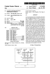
[54] HIGH SPEED COUNTER CIRCUIT
[75] Inventor:
Allen-Bradley User’s Manual “Encoder/Counter Mod
ule”, Catalogue No. l771—IJ,IK, 1981.
[73] Asslgnee: ?fsiizileywiompany’ Inc"
Primary Examiner-John S. Heyman
'
Attorney, Agent, or Firm-Quarles & Brady
[21] Appl. No.: 676,621
.
Oct. 20 9 1992
OTHER PUBLICATIONS
Gary Parker, May?eld Heights, Ohio
’
5 9 157 9 701
[57]
'
ABSTRACT
A high speed counter employs a number of functional
[22] Flled'
Mar‘ 28’ 1991
blocks, ?exibly interconnected on a bus structure, to
cogs/77A:
provide efficient and high speed implementation of
arbitrary range measuringmks A. set of independent
[52]
. . Cl. ...................................... .. 77/39, 37 {/5561
counters blocks are connected by the bus structure to
[58]
_
Field of Search ............................ .. 377/39, 54, 56
programmable comparator blocks which establish
count thresholds. The output of the comparators are
[51]
01.5 .......................................
'
[56]
_
paired by switchable AND/OR blocks to create ranges.
References C'ted
The division of functions by block and the interconnect
U.S. PATENT DOCUMENTS
3824378
ing bus structure allows the structure of each counter to
7/1974 Johnson et al. ..................... .. 377/39
4,305,123 12/1981 Scibor-Rylski
377/39
4,420,814 12/1983 Arikawa et al. ..
377/39
4,809,221
7
,_
hand‘
2/1989 Magliocco et a]. ................. .. 377/39
_
_
?
_
_
6 W |
_
_
__
_
5 Claims, 6 Drawing Sheets
..
_
_
_
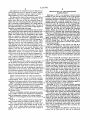
rss
| ~l> COUNTER
\>
I
‘:i)
182(0) 84
:
’
‘
REG
____:> MUX Q:|o3(u) 1
1
._
_
1
.
7
%-2;>
: _’_
88‘
In 98"’) ‘00M
l
l FD COUNTER
MUX
3
I j
|
I _ _
> ->
)
L
‘
l
REG :>
3
3
\ samq
.2
)
7
j
- -
‘
°
LHOM) I
I08(b)
> -.-_
= 2.,
I
|
L < H'load)
RE;
104(c)
‘m5
“LL? MEX Q: 103(d) + 4 :>
82(d) 84(dl/ _,
OR/AND 7;“ )
=___\_
I04(b)
i
' l
>
98(c) I0O(c)
|
72/1
mmj
3
L82“) 84k,
as’ l “9 couirrsR
'03“)
'
"39(0)
REG
r \
_'
|
L I04(o)
< “T
loztbh
.
\—82(b) saw)
__
> --.>
x’ ?'>
1 98(0) 100(0)
(
(c)
|
l
__
- —
8i i MD coug-l-Eq ) 211mg MLZJX CD3“), I, 2 :>
|
__
—
>
80
be effectively Programmed ‘0 ?t ‘he applicatim‘ 3‘
|64(b)
I am
> _,
: ___
OR,,TD_L
_
|
I
Lnow) I
|
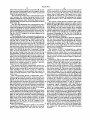
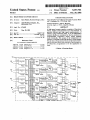
US. Patent
Oct. 20, 1992
_
I
__
.
_
MODE
com
‘62
Q
I
I
‘
'36
42
v
LJ
BUS
INTERFACE
~76
\
I
I
I
Bl
I
I
I
___£54
it?
AN
SYNC
I
Sheet 1 of 6
Z9
5,157,701
US. Patent
Oct. 20, 1992
Sheet 2 of6
I
COIURTP S
CINRPUTS
MICRO
PROCESSOR
COUNTER
SYSTEM
34
54
BACKPLANE
2I
5,157,701
US. Patent
Oct. 20, 1992
Sheet 4 of 6
5,157,701
(aI-(d)
_
_
_
RE
I
I
I
93
I
J@ ra? :
I
CLEAR
|
REG
24 BIT
99
21’:
I-->
I
I (UNDERW C we“
I
I
..
3
I I
/86
as
u I: LOAD
92:
I
.
I
:>
|
I
I
lam)
I
@I
88x
J
I
_
l 84(d)
@
i) REG ——___—L>
I
'
|
(
78 i
I
_I____
I
80 I
Q)‘
\‘
_ .1
‘
(OVERF
>
_£82__
@D]
I
I
II
I
1
<
I
I
\F' I
I
I
I
’
I
I
/._ I
I
\r' I
|
L
__
.~
_
_
_
I
_ __ __
I
w
US. Patent
Oct. 20, 1992
Sheet 5 of 6
I
64(0)
1
5,157,701
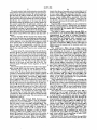
I
I<
I
I
MODULUS 30o
>I
I
I
0
I00
200
COUNT-+
299
J‘:
A,
FFFFFFIG
FIG. 6
I
l
K
I
MODULUS 300
>:
. I
I
|
I
64(o)\
o
50
A‘
tr
7 250 299
JI
FFFFFFIS
COUNT-P
FIG. 7
I
I
K
I
MODULUS 300
)1
|
I
64(0“ |
I
64w)1 0I
‘
I00
-
I25
I75
COUNT—*'
FIG. 8
I
zaieg“
J‘
FFFFFF'G
US. Patent
Oct. 20, 1992
Sheet 6 of 6
5,157,701
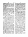
{I20
FIG. 9
/
4
\
|22\
W
x
lololo] I
OUTPUT 0 M88 (ON)
OUTPUT 0 L58 (ON)
OUTPUT 0 M58 (OFF)
\ OUTPUT 0 L58 (OFF)
X
Jlll
OUTPUT 64(0)
.
5,157,701
1
HIGH SPEED COUNTER CIRCUIT
BACKGROUND OF THE INVENTION
1. Field of the Invention
The ?eld of the invention is industrial control systems
including programmable controllers, and more particu
larly, a high speed counter module used in conjunction
with such industrial control systems.
2. Background Art
Industrial control systems such as those described in
U.S. Pat. Nos. 3,810,118, 3,942,158, 4,165,534 and
4,442,504 are typically connected to industrial equip
ment such as assembly lines or machine tools, to operate
such equipment in accordance with a stored program.
The stored program, running on the central processing
unit of the system, termed the “controller”, includes
instructions which, when executed, examine the condi
2
controller on a less frequent basis to determine if a given
count has been reached.
An improvement to the use of separate counter mod
ule is the combining of a counter with one or more
comparators to constantly evaluate the count against
threshold values‘and to produce a binary signal indicat- _
ing whether or not the count has exceeded the thresh
old value. This use of the comparator frees the control
ler from repeatedly loading the multi-bit count and
10 comparing it to a threshold value in its program.
Rather, the comparator allows the controller to exam
ine only the single bit of the comparator’s output repre
senting the state of the count withrespect to the thresh
old value.
With more complex systems it may become necessary
to evaluate the count of a counter against a number of
thresholds. For example, it may be desirable that the
program runningin the controller execute a ?rst task
when the count reaches a ?rst value and execute a sec
tion of selected inputs to the system from sensing de 20 ond task only if the count reaches a second value and so
vices on the controlled equipment and energize or deen
forth. This may be accomplished by wiring several
comparators to each counter so that different thresholds
ergize selected outputs from the system to operate de
vices on the controlled equipment.
Inputs to the system may be discrete binary signals
I such as those from switches, which may detect limits of
process variables such as motion, temperature, time, or
other quantities, or the inputs may be analog measures
of the process variables themselves, which are generally
then converted to digital binary form for processing.
Likewise, the outputs of the system may be either bi
nary outputs as implemented by mechanical or solid
state relays, or analog outputs produced by means of a
- digital to analog converter.
A process variable, such the number of items moving
along an assembly line, may be counted by the control
ler by means of a sensing device which sets and resets a
single digital input to the controller for each passing
item. The changes in that input may be tallied by means
of the program running in the controller.
This approach to counting has two signi?cant draw
backs. The ?rst is that only relatively low count rates
may be supported by the controller. Typically, the in
may be established.
Ultimately, the disadvantage of implementing the
counting function in “hardware”, (that is discrete circu
ity), rather than through the “software” of the control
ler, is that the counting function is much less ?exible.
The number of threshold values is ?xed by the counter
circuitry and cannot be increased as the application may
demand. For this reason it is the practice to provide
each counter with a number of extra comparators for
producing additional thresholds. Counters having as
many as four different threshold values are commer
cially available, but even this number may be too little
for some applications. Further, the extra cost of the
unused threshold circuitry may be signi?cant in cases
where only one threshold value is needed.
SUMMARY OF THE INVENTION
The present invention provides the counting speed
associated with a “hardware” implementation of the
counting function, and yet provides much of the ?exi
bility normally associated with a “software” implemen
tation of the counting function. This is accomplished by
puts and outputs of the controller are “scanned” one at
a time, the state of each output and input being sequen 45 dividing the counting function into a number of discrete
tially written to or read during each scanning cycle. If
the counting rate is higher than the scanning rate, some
“counts” will be lost.
_
For many applications, and in particular, those appli
cations where the items to be counted are pulses from a
high resolution encoder or the like, the limit imposed by
the scanning rate will be unacceptably low. Further,
because the actual scan rate varies depending on how
many inputs and outputs must be scanned, the maximum
logical units which are implemented in hardware and
joined by a programmable bus structure to allow the
various logical units to be ?exibly interconnected. The
result is that the counter of the present invention may be
programmably con?gured ef?ciently to ?ll the needs of
a number of counting applications.
Speci?cally, a set of independent counters provides a
counter output to a bus. Multiplexers receive the
counter outputs from the bus and communicate one
count rate must be given an additional margin of reduc 55 counter output to the input of one digital comparator of
tion to ensure reliable counting under a “worst case"
a set of digital comparators corresponding in number to
analysis of scan time. Such worst case analysis must take
the multiplexers. The other input of each digital com
into account possible future expansion of the controls
system to include additional inputs and outputs.
parator is provided by a programmable register holding
a threshold value.
The second drawback to the above approach to 60
It is one object of the invention to allow the compara
counting is that the controller is diverted from other ' tors to be ?exibly assigned to any one of the counters,
control tasks by the need to repeatedly examine the
thus allowing one counter to have up to the maximum
particular input being counted and to execute a portion
number of provided threshold values or any number
less than that maximum. The multiplexers and bus struc
of its program to count that input signal.
Accordingly, it is known to use a separate binary 65 ture permit this assignment to be accomplished under
. counter module communicating with the controller to
the direction of the controller to which the counter
independently count such process variables. The binary
count produced by the counter may then be read by the
module is attached, thus providing an effective degree
of programmable ?exibility to the counter structure.
3
5,157,701
4
The outputs of the comparators may be linked by an
AND/OR gating circuit to provide an output, indicat
ing whether a particular counter output is within a
DESCRIPTION OF THE PREFERRED
EMBODIMENT
Referring to FIG. 1, an industrial control system
range de?ned by two or more threshold values.
It is thus another object of the invention to provide an 5 suitable for use with the counter circuit of the present
invention includes a programmable controller 10 com- .
additional degree of independent processing of the
municating through a backplane 12 with adjacent I/O
count value, and thus to free the controller from the
modules 14 within a rack 16. Additional remote I/O
simple, but time consuming, Boolean operations neces
modules 18 may be contained within one or more re
sary to generate a signal indicative of a range and de
?ned by a combination of threshold values. The use of
mote I/O racks 20 connected to the programmable
controller 10 via a serial remote I/O link 22. The pro
an AND/OR gating circuit provides a high degree of
?exibility in constructing that range.
grammable controller 10 sequentially addresses each
remote I/O rack 20 and the modules 18 contained
therein. Within each remote rack 20, the data of the
serial link 22 is decoded and transmitted along back
plane 21 to communicate with each of the modules 18.
The multiplexers may be controlled by data in associ
ated registers and these registers and the registers hold
ing the threshold values may be written to by the con
troller. The counter may be con?gured by data words
The remote l/O racks 20 may be located up to 5000
feet from the programmable controller 10. A program
mable controller with remotely located I/O racks is
registers where each data block is associated with each
disclosed
generally in Markley et. al. U.S. Pat No.
20
comparator pair, as joined by an AND/OR gating cir
3,997,879, issued Dec. 14, 1976 and entitled: “Fault
cuit. A ?rst word of the data block indicates a ?rst
Processor for Programmable Controller with Remote
threshold value for the ?rst comparator of the AND
I/O Interface Racks.”
/OR gating circuit, and a second word indicates a sec
The data throughput of the remote I/O link 22 is
ond threshold value for the second comparator of the
limited by its serial format. This limit of data through
AND/OR gating circuit, the second threshold value
put may be important for certain high speed I/O func
together with the ?rst threshold value de?ning the
tions or when a large number of remote I/O racks re
range output, and a third word indicates from which
quire the scanning of many I/O addresses. Of particular
independent counter, or counters, the counter output
importance are digital encoder or counter inputs whose
will be received by the ?rst and second comparators.
high data rates may tax the data throughput of the link
22 if they trans'mit directly on the ‘link 22, as described
Thus, it is yet another object of the invention to pro
above.
vide a natural command structure for changing the
A counter module 24, according to the present inven
architecture of a hardware counter in response to com
tion, serves to limit the data throughput required to
mands from a controller.
support high data rate encoders or counters, by per
The foregoing and other objects and advantages of
forming counting and range comparison functions at the
the invention will appear from the following descrip
module level, rather than at the controller level, i.e.,
tion. In the description, reference is made to the accom
through a program running on the programmable con
panying drawings which form a part hereof and in
troller. The counter module 24 is received with other
which there is shown by way of illustration, a preferred
remote modules 18 into the remote rack 20, and may
embodiment of the invention. Such embodiment does
accept a pulsed DC or binary signal from a rotary en
not necessarily represent the full scope of the invention,
coder 26 or the like. As is generally understood in the
however, and reference is made therefore to the claims
art, the rotary encoder 26 produces two square wave
herein for interpreting the scope of the invention.
‘signals along separate leads 28 whose relative phases
indicate the direction of the rotation 30 of the shaft of
BRIEF DESCRIPTION OF THE DRAWINGS
held in a number of data blocks transmitted to these
the encoder 26 and whose number of square wave cy
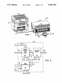
FIG. 1 is a pictorial view of an industrial controller
communicating with a remote rack of I/O modules
cles indicate the number of degrees of rotation 30. Al
ternatively the counter module 24 may receive a single
lead (not shown) from a sensor indicating simply a
including the counter module of the present invention;
FIG. 2 is simpli?ed schematic of the counter module
of FIG. 1 showing the interconnection of a controlling
microprocessor with the counter system circuitry;
count magnitude without a count direction.
Referring to FIG. 2, the counter module operates
under the control of an on~board microprocessor 34.
Microprocessor 34 is a general purpose sixteen-bit mi
croprocessor, such as the Intel 80Cl88, which provides
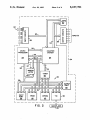
FIG. 3 is a simpli?ed schematic of the counter system
circuitry of FIG. 2 showing the data paths to and from
the counter array;
55
eight bi-directional data lines 36, eight dedicated ad
dress lines 38’, and a variety of control lines 44 and 56.
The address lines 38' comprise the higher ordered
eight bits of a sixteen bit address ?eld. The lower or
dered eight bits of the sixteen bit address ?eld are pro
vided by the data lines 36, which are multiplexed to
FIG. 4;
include both data and address information, and decoded
FIGS. 6, 7, and 8 are graphs showing various exam
by address latch 40, receiving data lines 36 and address
ples of outputs from the counter module of FIG. 1;
enable line 42, to latch the lower eight bits of the ad
FIG. 9 is a pictorial representation of a data block
dress ?eld, as is generally understood in the art; and,
used to con?gure the counter module of FIG. 1; and 65 when combined with address lines 38, to produce six
FIG. 10 is a timing diagram showing the relative
teen bits of address 38.
timing of the signals used to control the counters of
The sixteen address lines 38 form one-third of an
internal bus 32. Data lines 36 make up an additional
FIG. 5.
FIG. 4 is a simpli?ed schematic showing the counter
array of FIG. 3 and the bus architecture connecting a
bank of independent counters with various outputs;
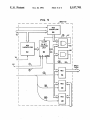
FIG. 5 is a block diagram of each of the counters of
5,157,701
5
6
cessed by theinput circuits 58, the twelve input signals
third of the internal bus 32, and control lines 44, provid
ing read/write timing signals and clock signals, such as
62 are received by the counter system 54 and also re
are generally understood in the art, make up the ?nal
third of the internal bus 32.
The internal bus 32 provides a communications path
way between the various functional blocks of the
counter module 24, to be described, and provides com
munications between these functional blocks and the
programmable controller 10 via the backplane 21 and a
ceived by the lamps 50, the lamps which indicate the
binary state of each signal. The signal from a rotary
TIC “chip” 30.
The TIC chip 30 handles the communication proto
col necessary for receiving and transmitting data be
encoder26, for example, may be received by one chan
nel 60; the rotary encoder 26 producing two phased
signals received by the A and B inputs of the channel
60.
The counter system 54 also produces eight output
10
signals 64(0) through 64(h), received by output circuits
tween the backplane 21 and the internal bus 32 for the
6 and by lamps 50, which indicate the binary state of
each signal 64. The output circuits 66 convert the logic
level signals from the counter system 54 to switched
counter module 24. A detailed description of a circuit
outputs, which provide user accessible open or closed
for accomplishing these communication protocols, suit
circuits ‘depending on the state of the respective signal
able for use with the present invention, is given in U.S.
Pat. No. 4,937,777, assigned to the same assignee as the
present invention.
64. An output circuit suitable for use with the present
invention is described in U.S. Pat. No. 3,745,546 as
signed to the same assignee as the present invention and
The internal bus 32 also communicates with an eras
able programmable read-only memory (“EPROM”) 45,
a static random access memory (“SRAM”) 46, an input
port 48, and an output port 50, each which may be
addressed and read or written to by microprocessor 34
through address lines 38 and data lines 36. The EPROM
20
also incorporated by reference.
Thus, the counter system 54 is generally integrated
into the above described microprocessor architecture
and may communicate with the backplane 21, the input
circuits 58, or output circuits 66 through the various
signal paths described above. The counter system 54
45 contains the “?rmware” program executed by the 25 also receives a time signal 53 in the form of a periodic
square wave of predetermined frequency from the timer
microprocessor 34 in conjunction with the operation of
52, previously described.
the counter module 24, that operation to be described in
The circuitry of FIG. 2 is assembled on a printed
‘ detail. The SRAM 46 provides “scratchpad” storage
space for data manipulated by the microprocessor 34,
and provides storage areas that may be read by the
programmable controller 10 through the TIC chip 30.
The input port 48 optionally allows certain values to be
circuit board to which the various components are
soldered. Counter system 54 is a custom large scale
integrated circuit. Screw terminals, as are understood in
the art, provide access to the input circuits and the
output circuits, and the indicator lamps are light emit
ting diodes.
ers. The output port 50 allows the microprocessor 34 to
display information on front panel indicator lamps 50, in 35 Referring to FIG. 3, the counter system 54 receives
the input signals 62 through mode control and synchro
particular, an indicator showing whether the counter
input to the microprocessor 34 by programmable jump
module 24 is running properly or whether a fault has
occurred, as is well understood in the art.
.
The internal bus 32 also communicates with a pro
nization circuitry 68 which serves two principle pur
poses. First, the input signals 62, derived from rotary
encoders 26 or the like, as shown in FIG. 1, are gener
grammable timer 52 which provides a precise time base 40 ally asynchronous with respect to the internal timing of
for the counter module 24 for period and rate measure
the counter module 24. The mode control and synchro
ment techniques, well known in the art, where the
count value is gated by a user-de?ned time interval to
yield an average frequency value, rather than simply a
nization circuitry 68, therefore, is used to synchronize
these input signals 62 to the internal timing of the
counter module 24 by means of tandem, gating ?ip-?ops
count total.
.
(not shown) as is understood in the art. Second, the
mode control and synchronization circuitry 68 provides
The microprocessor 34 also communicates with a
counter system block 54 by means of data lines 36, con
trol lines 44, the address enable line 42, and'a chip select
. timing and gating signals to permit the counter system
data is provided by the address information multiplexed
countdown signal compatible with dual clocked
to operate in a number of modes: In an encoder mode
(1), the phased square wave signals from a rotary en
line 56, so as to control the counter system 54 and pro
vide communication between the counter system 54 and 50 coder 26 and received by inputs “A” and “B” (as shown
in FIG. 2) are interpreted into a count-up signal or a
the backplane 21, as will be described below. Address
counter, the latter of which will be described further
on the data lines 36, as has been described, and by the
chip select line 56 which serves in lieu of the higher
below. In a counter mode (2), the A input is counted,
55 and the B input determines whether the counter counts
order address lines 38' otherwise required.
up or down in response to A. In a period/rate mode (3),
The counter system 54 also receives inputs from input
the counter counts an internally generated four mega
circuits 58. Input circuits 58 process the signals to be
hertz clock signal 53 (shown in FIG. 2), which is gated
counted by the counter module 24 on lines 28 (shown in
by the presence of a signal on the G input for the given
FIG. 1), and perform electrical isolation and ?ltering
channel 60. Thus, the count will reflect the time period
functions to make the input signals compatible with the
of the gate signal. In a rate mode (4), a count at input A
logic levels of the counter module circuitry. An input
is counted for a period of time derived from the signal
circuit which may be used with the present invention is
53 from timer 52. The methods and techniques for pro
described in U.S. Pat. No. 4,275,307 assigned to the
viding these functions are well understood in the art,
same assignee as the present invention and hereby incor
65 and for clarity, this circuitry will not be discussed fur
porated by reference.
ther except with regard to certain timing signals which
The input circuits 58 receive signals to be counted
through four channels 60(a)(d) each channel having of
are required for the operation of the later described
three terminals termed “A”, “B”, and “G”. As pro
counters.
7
5,157,701
8
twenty-four-throw, four-pole switch connecting one of
The mode control and synchronization circuitry 68 is
controlled by instructions received by the microproces
sor 34 via bus interface circuitry 70, which accepts the
data lines 36, the address enable 42, the chip select line
counter outputs 84 from counter 82(0) through 82(d) to
its own output 100. The particular selection or pole
position of each multiplexer 98 is determined by a value
set in a register 103(0)—103(c), associated with each
56, and control lines 44 so as to communicate data be
tween the microprocessor 34 and the counter system 54.
Speci?cally, the combination of the data lines 36 and
the address enable line 42 allows the various registers of
the counter system 54 to be addressed, written to, and
multiplexer and receiving a program word from the .
data bus 76 as addressed by the enable signal 78 from the
bus interface 70.
Registers 102(0) through 102(p) are also connected to
read from, without the need for separate, external pins
carrying the lower ordered address. This provides a
considerable savings in interconnecting pathways on
the counter system chip 54 and allows the sharing of the
same eight pins of the custom integrated circuit forming
data bus 76 and receive a twenty-four bit threshold
word as programmed by the user through the program
mable controller 10. One register 102 is associated with
each multiplexer 98.
The output of each counter 82(0) through 82(d), as
transmitted by each multiplexer 98(0) through 98(p), is
the counter system 54 for both address and data infor
communicated to one input of a digital comparator
mation.
104(0) through 104-(p), the other input of which receives
The bus interface 70 also decodes the address infor
the twenty-four bit threshold word contained in the
mation from the data that is multiplexed on data lines 36
corresponding register 102. Thus, for example, multi
and produces a set of enable signals 78 for controlling
various registers, to be described, allowing new values 20 plexer 98(0) provides a twenty-four bit output word to
to be entered into or read from those registers by the
one input of comparator 104(0), and the other input of
104(0) receives the twenty-four bit threshold word from
user, through the programmable controller 10—the
register 102(0).
‘registers serving generally to hold the con?guration
data for the counter array 72 and to store various count
The comparators 104(0) through 104(p) produce
values.
25 three outputs, only one of which may be high at a given
time depending on the inputs to the comparator 104
A counter array 72, communicating both with the bus
interface 70 and the mode control and synchronization
from the multiplexers 98 and the registers 102. These
circuitry 68, receives four pairs of dual clock signals 80
synchronization circuitry 68, and receives an eight bit
data bus 76 and corresponding control signals 78 from
three outputs from the comparators 104 indicate respec
tively whether the output from the multiplexer 98 is
greater than, is equal to, or is less than the'threshold
value in register 102. Each of these comparison outputs
the bus interface 70. The data on the data bus 76 is
identical to the data on data lines 36 of bus 32. The
108(0) through 108(p), constructed of three dual input
and certain control lines 81 from the mode control and
106 is received by a three input switchable OR gate
controls signals 78 enable various registers, as will be
and gates having outputs received by a three input OR
described.
35 gate, which logically OR’s selected ones from among
the three outputs of the comparators 104. The selected
The counter array 72 produces the eight output signal
outputs, gated by the AND portions of the switchable‘
64(0) through 64(h) from the counter system chip 54.
Referring now to FIG. 4, the architecture of the
OR gate 108(0) through 108(1)), are determined by a
counter array 72 allows ?exible interconnection among
value stored in a register.(not shown) associated with
a number of functional blocks which together produce 40 each switchable OR gate 108(0) through 108(p), the
the desired counting function. These functional blocks >
are counters 82(0)-82(d), comparators 104(0)-104(d)
and their associated registers, and AND/OR gating
circuits 110(0)-110(k). The independent counters 82(0)
through 82(d) each receives a separate dual clock signal
80, and each receives the internal data bus 76 and con
trol lines 78 (not shown in FIG. 4 for clarity). Each dual
clock input signals 80 consists of two lines, only one of
which may receive a clock input at a time. The ?rst line
is a “count-up” line and indicates, as its name implies,
that the counter is to increment its total count value.
The second line of each dual clock signal 80 is the
“countdown” line and indicates that the counter should
register being loaded through the data bus 76 and ulti
mately by the user programming the programmable
controller 10, as described above.
Thus, depending on the setting of the switchable OR
gate 108, the output of the switchable OR gate 108 will
be high if the counter output 84 selected by multiplexer
98 is larger than, is equal to, or is less than the threshold
value in the register 102, or some combination of these
conditions provided by the OR portion of the switch
50 able OR gate 108.
The outputs from two switchable OR gates 108 are
connected to one of eight AND/OR circuits 110(0)
through 110(k), which may act as either an AND gate
decrement its total count value. This convention is well _ or as an OR gate, as controlled, and also by a register
understood in the art.
55 (not shown), as programmed by the user through the
Each counter 82(0) through 82(d) functions as a
twenty-four bit up/down counter, with an adjustable
programmable controller 10. Thus, the outputs of each
pair of switchable OR gates 108(0) and 108(b) are con
modulus from zero to FFFFFF16, to produce a twenty
nected to a single AND/OR gating circuit 110. The
four bit output count value 84(0) through 84(d). The
twenty-four bit output count value 84(0) to 84(d) of
each counter 82(0) through 82(d) is connected, by
outputs of the eight AND/OR gating circuits 110(0)
through 110(k) are the outputs 64(0) through 64(h) of
means of a counter output bus 96 comprised of four
the counter array 72, as previously described. This
matching of two switchable OR gates 108 to one AND
parallel twenty-four bit channels, to each of sixteen
/OR gating circuit 110 is continued for each of the
multiplexers 98(0) through 98(p). Each of these multi
switchable OR gates 108(0) through 108(p), producing
plexers 98 channels one of the twenty-four hit counter 65 eight output signals 64 corresponding to eight AND
outputs 84 from the counter bus 96 to that multiplexer’s
/OR gating circuits 110(0) to 110(k).
single twenty-four bit output 100(0) through 100(p).
The multiplexers 98 therefore operate as an effective,
Referring to FIG. 5, each counter 82(0) through 82(d)
of FIG. 4 is constructed around a twenty-four bit, load
5,157,701
able, up/down counter unit 83 receiving dual clock
lines 80, a load line 88 for loading its count value, and a
clear line 93 for setting the count value of counter 83 to
zero. The counter unit produces a twenty-four bit
counter output 85. The twenty-four bit counter unit 83
is functionally equivalent to a counter comprised of six
synchronously connected four bit TTL counters such as
the Texas Instrument 74192, as described in the “TTL
Databook For Design Engineers“, Second Edition,
Published by Texas Instruments, Inc., hereby incorpo
10
shown). During a count-up, as shown in FIG. 10, the
countdown signal II is high and the output of counter 83
is incremented on the rising edge of the count-up signal
I. A latch signal “III” for register 112, produced by the
mode control and synchronization circuitry shown in
FIG. 68, is delayed for one clock period of the eight .
Mhz clock. In between the rising edges of the up count
signal I and the rising edge of latching signal III for
register 112, signals “VI” or “V”, indicating under?ow
or over?ow condition and generated by AND gate
rated by reference.
The adjustable modulus feature of the counters 82(0)
through 82(d) is realized as follows: An under?ow, that
is, when the counter 83 is counting down and its count
value becomes FFFFFF16, is detected by an AND gate
circuit 86 or EXCLUSIVE OR gate circuit 92, if an
over?ow or under?ow exists for the given count, will
circuit 86 which receives the output 85. The AND gate
circuit 86, detecting the zero state of the counter output
85 produces a load signal on load line 88 that causes the
counter unit 83 to load an under?ow value from register
90, as determined by the user and loaded in register 90 20
as has been described, prior to the rising edge of the
latch signal III.
Two additional registers 116 and 118 store counter
through the programmable. controller 10. The under
produce a pulse with a rising edge prior to the rising
edge of signal 111.
This signal VI or V loads or clears the counter unit 83
output values 85. Register 116 is triggered by signal IV,
similar in timing to signal III, and allows reading of the
output 85 by microprocessor 34 without interruption of
the outputs 84(0)—84(d). Register 118 is used to capture
?ow value in register 90 is equal to one less then the
a particular count value as triggered by signal VII de
desired modulus of the counter 82. Thus, when counter
rived from the G input of input circuit 58 (shown in
unit 24 under?ows, it receives the under?ow value
contained in register 90 rather than under?owing to its 25 FIG. 2) and as processed by the mode control and syn
chronization circuitry of 68 of’ FIG. 3. Register 118 is
maximum count value of FFFFFF16.
generally triggered asynchronously with respect to
The output of counter unit 83 is also received by
register 116 but is delayed with respect to the signals I
EXCLUSIVE OR gate circuit 92, which compares that
or II, like registers 112 and 116, to insure that no spuri
output to an over?ow value held in register 94, as deter
ous output values 85 are captured by these registers.
mined by the user.
The outputs of these registers 116 and 118 may be ac
The over?ow value held in register 94 is exactly one
cessed by the user through the programmable control
more than the under?ow value held in register 90. Thus,
ler 10 and microprocessor 34 by means of the internal
when the output of the counter unit 83 equals the over
data bus 76.
?ow value contained in register 94, a clear signal is
created on the clear line 78 which resets the counter 35
unit 83 to zero.
Accordingly, referring to FIG. 4, it will be under
stood that the user may program a number of features of
the counter array 72: l) the modulus of each counter 82
As with the other registers, registers 90 and 94 are
may be controlled separately; 2) by virtue of the multi
connected to the data lines 76 and enabling control lines
plexers 98(0) through 98(p) the output of each counter
78 so that their values may be loaded from the program
mable controller 10 via the remote link 22, through the 40 may be associated with any output signal 64; and 3) each
output 64 may have a “turn on” and “turn off" point
TIC chip 30 and the internal bus structure of the
anywhere within the modulus of its associated counter
counter module 24, as previously described. It will be
82. It should be understood, also, that a given output
understood from this description that an arbitrary mod
signal 64 may be associated with either one or two
ulus for the counter 82 through 82(d) may be thus estab
lished simply by programming the registers 90 and 94 45 counters. That is, optionally, the “turn on" point may be
determined by one counter, and the “turn off” point
with under?ow and over?ow values respectively.
may be determined by a second counter.
Referring still to FIG. 5, it is noted that the over?ow
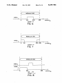
Referring to FIG. 6, the modulus of a counter 83 may
value held in register 94 is in fact one greater than the
be set to 300 by programming register 90 shown in FIG.
maximum value counted to by the counter unit 83,
given the desired modulus of the counter unit 83. As a 50 5 with 299 and register 94 shown in FIG. 5 with 300.
The counter 82 associated with those registers will then
result of the intrinsic gates delays of the EXCLUSIVE
count between the values of zero and 299.
OR gate circuit circuit 92, which detects when counter
Output 1 may be associated with that counter 82 by
unit 83 has reached the count indicated by the value of
loading the appropriate values in the registers associ
register 94, for a brief period of time, the counter unit 83
will output a spurious count value 85. For similar rea 55 ated with multiplexers 98(0) and 98(b) so that, for exam
ple, the output of counter 82(0) is switched to compara
sons during an under?ow of counter unit 83 and be
cause of the intrinsic gate delays of AND gate circuit 86
tor 104(0) and 104(b). If it is desired that output 64(0)
turn on beginning at count 100, register 102(0) may be
during an under?ow condition, the counter unit 83 will
loaded with the value 100 and both the “greater than”
display its maximum count of FFFFFF16 prior to being
and “equal” bits set with regard to the register control
loaded with the under?ow value in register 90 per the
ling the switchable OR gate 108 to detect the greater
de?ned modulus of counter 83.
Accordingly, the outputs of the counters 84(0)
through 84(0') in fact come through a register 112,
than OR'equal condition. Alternatively, register 102(0)
may be loaded with the value of 99 and only the greater
than bit set in switchable OR gate 108(0).
_. which is gated so as to ignore any spurious transitional
If it is then desired that the output turn off at count
values from counter unit 83. Referring also now to FIG. 65
200, register 102(b) may be loaded with the value 200
10, the count-up or countdown signals “I” or “II” are
synchronized, as previously described, with an eight
Mhz clock signal 114 from an onboard clock (not
and the “greater than” and “equal” bits set in register
controlling the switchable OR gate, or alternatively,
11
5,157,701
register 102(b) may be set with the value 199 and the
“greater than” bit set. In either case the AND/OR
circuit 110 will be con?gured by the user for the AND
con?guration so that the output 64 is on when the count
is greater then 100 and less then 200.
In a second example shown in FIG. 7, the output may
12
A preferred embodiment of the invention has been
described, but it should be apparent to those skilled in
the art that many variations can be made without de
parting from the spirit of the invention. For example,
the number of counters and outputs may be increased
within the architecture described above. In order to _
be set so that it turns off when the count is greater than
50 and then on again when the count is greater than
apprise the public of the various embodiments that may
fall within the scope of the invention, the following
250. Here register 102(0) may be loaded with the value
50 and the “greater than” and “equal” bits set on the
register associated with the switchable OR gate 108(0).
Register 102(b) may be set with the value 250 and the
“less than” and “equal” bits set with respect to the
switchable OR gate 108(b). Here the AND/OR circuit
110(0) would be con?gured in the OR mode so that the
claims are made.
output 64(0) is on when the count is less than or equal to
50 or greater than or equal to 250.
Importantly, two or more outputs 64 may be con?g
ured to be associated with a single counter 82. In FIG.
8, output 64(0) is con?gured to turn on when the count
is greater than 125 and turn off when the count is
greater than 175, whereas output 64(b) is con?gured to
turn on when the count is greater than 5 and less than
100. In this case multiplexer 98(0), (b), (c), and (d) are all
con?gured to select the same counter 82(a) so that both 25
outputs 64(0) and outputs 64(b) may indicate the state of
that counter 82(0).
Referring to FIG. 2 and 9, each of these above de
scribed con?gurations and many other con?gurations
of the architecture of counter module 24 are pro
grammed simply by a data block 120 held in SRAM 46,
as loaded by the user through the programmable con
troller 10. Each of the eight outputs 64 of the counter
module 24 has ?ve data words 122 associated with it.
The ?rst four bits of the ?rst data word 122 for each 35
output 64 indicate which of the four counters 82(0)
through 82(0') is associated with that output 64. Only
one bit of the ?rst four bits in this ?rst data word 122
may be set. The next two data words 122 contain the
most signi?cant bits and least signi?cant bits of the 40
twenty-four bits to be loaded into the ?rst register 102
I claim:
1. A high speed counting unit comprising:
a plurality of independent counters each having an
input for receiving a count signal and each having
a counter output indicating a total count value;
a plurality of ?rst registers each for holding a counter
address;
a plurality of multiplexers, each multiplexer having
plural multiplexer inputs communicating with each
of the independent counters to receive the counter
outputs, and address input for receiving a one
counter address, and each multiplexer for selec
tively communicating at least one counter output
to a multiplexer output for that multiplexer as des
ignated by one counter address;
a plurality of second registers corresponding in num
ber to the multiplexers, each register for holding a
threshold value; and
g
a plurality of comparators corresponding in number
to the multiplexers, each comparator communicat
ing with a second register for receiving the thresh
old value from that second register as a ?rst input
and communicating with the multiplexers for re
ceiving the multiplexer output from that multi
plexer as a second input, the comparator for pro
ducing a threshold output dependant on the rela
tive magnitudes of the ?rst and second inputs.
2. The high speed counting unit as recited in claim 1
including:
a plurality of AND/OR gating circuits communicat
ing with at least two comparators for receiving the
threshold outputs from those comparators for pro
associated with that output 64. These bits are termed the
ducing a range output depending on a Boolean
“on bits”, referring to the example of FIG. 6 where
these bits determine the point at which the output turns
combination of the threshold outputs.
on. The next two data words 122 are the most signi? 45
cant bits and least signi?cant bits of the twenty-four bit
“off word” which is loaded into the second register
102(1)) associated with that output 64. This data block
120 is repeated for each of the eight outputs 64. ‘
Referring generally to FIG. 2, it can be seen that this
simple data structure and the particular functional divi
sion of the counter array 76 as described above allows
virtually unlimited ?exibility in con?guring the eight
outputs 64 among the four counters 82. For example, all
eight outputs 64 may read one counter 82, providing a 55
3. The high speed counting unit as recited in claim 1 .
wherein the comparators comprise:
a magnitude comparator unit for receiving the ?rst
and second input and for producing three outputs
indicating respectively when the ?rst input is
greater than, equal to and less than the second
input; and
a gated input three input OR circuit for receiving the
three outputs and for producing a signal that is the
logical OR of at least one of the three output sig
nals.
4. The high speed counting unit as recited in claim 1
set of staggered or overlapping digital outputs depen
wherein the counters are variable modulus up/down
dant on the value in that counter 82. Conversely, the
counters.
eight outputs 64 may be distributed among the four
counters 82 providing each counter with two outputs
64. Many other combinations are possible.
The functional division of the counters 82 from the
output comparators 104, and from the AND/OR gating
circuits 110 and the use of the bus structure 96 for con
necting any output 64 to any counter 82, thus provides
a high degree of ?exibility in con?guring a counter 65
module 24 to a particular process, yet still allows the
high speed performance associated with a hardware
implementation of the counting function.
5. A data structure for controlling a high speed count
ing unit, the counting unit having:
a plurality of independent counters, each having an
input for receiving a count signal and each having
a counter output indicating a total count value;
a plurality of ?rst registers each for holding a counter
address;
a plurality of multiplexers, each multiplexer having
plural multiplexer inputs communicating with each
of the independent counters to receive the counter
outputs, and each multiplexer for selectively com
13
5,157,701
14
municating at least one counter output to a multi
ceiving the threshold outputs from those compara
plexer output for that multiplexer as determined by
tors and for producing a range output depending '
on a Boolean combination of the threshold outputs,
one ?rst data register;
a plurality of second registers corresponding in num
ber to the multiplexers, each register for holding a
the data structure comprising:
a multi-word data block for each ?rst and second
threshold value; and
a plurality of comparators corresponding in number
to the multiplexers, each comparator communicat
ing with a register for receiving the threshold value
from that register as a ?rst input and communicat l0
ing with the multiplexers for receiving the multi
plexer output from that multiplexer as a second
input, the_compara':or for producing a threshold
output dependant on the relative magnitudes of the
15
?rst and second inputs
a plurality of AND/OR gating circuits communicat
ing with each ?rst and second comparator for re
20
25
35
45
55
65
comparator, the data block having a ?rst word _
indicating a ?rst threshold value for the ?rst com
parator and a second word indicating a second
threshold value for the second comparator, the
second threshold value together with the ?rst
threshold value de?ning the range output, and a
third word indicating from which independent
counter the counter output ‘will be received by
each ?rst and second comparators, the data block
for transmission to the plurality of ?rst and second
registers of the high speed counter.
‘
t
t
i
‘