1
RF Development Platform
Designer Reference Manual
M68HC08
Microcontrollers
DRM068
Rev. 0
04/2005
freescale.com
RF Development Platform
Designer Reference Manual
by: Diego Garay
Daniel Torres
Jaime Herrero
Sergio Garcia de Alba
Applications Engineering, Guadalajara Applications Lab
Freescale Semiconductor, Inc., Guadalajara, Mexico
To provide the most up-to-date information, the revision of our documents on the World Wide Web will be
the most current. Your printed copy may be an earlier revision. To verify that you have the latest
information available, refer to http://www.freescale.com
The following revision history table summarizes changes contained in this document. For your
convenience, the page number designators have been linked to the appropriate location.
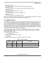
Revision History
Date
Revision
Level
April, 2005
0
Description
Initial release
Page
Number(s)
N/A
RF Development Platform, Rev. 0
Freescale Semiconductor
3
Revision History
RF Development Platform, Rev. 0
4
Freescale Semiconductor
Table of Contents
Chapter 1
Introduction and Setup
1.1
Introduction . . . . . . . . . . . . . . . . . . . . . . . . . . . . . . . . . . . . . . . . . . . . . . . . . . . . . . . . . . . . . . . .
1.2
RFDP Baseboard (Key Features) . . . . . . . . . . . . . . . . . . . . . . . . . . . . . . . . . . . . . . . . . . . . . . .
1.3
QF4 (Key Features) . . . . . . . . . . . . . . . . . . . . . . . . . . . . . . . . . . . . . . . . . . . . . . . . . . . . . . . . . .
1.3.1
Microcontroller . . . . . . . . . . . . . . . . . . . . . . . . . . . . . . . . . . . . . . . . . . . . . . . . . . . . . . . . . . .
1.3.2
UHF Transmitter Module . . . . . . . . . . . . . . . . . . . . . . . . . . . . . . . . . . . . . . . . . . . . . . . . . . .
1.3.3
MC908QF4EVB . . . . . . . . . . . . . . . . . . . . . . . . . . . . . . . . . . . . . . . . . . . . . . . . . . . . . . . . . .
1.4
Demonstration Software . . . . . . . . . . . . . . . . . . . . . . . . . . . . . . . . . . . . . . . . . . . . . . . . . . . . . .
1.4.1
Home (Key Features) . . . . . . . . . . . . . . . . . . . . . . . . . . . . . . . . . . . . . . . . . . . . . . . . . . . . .
1.4.2
RKE (Key Features) . . . . . . . . . . . . . . . . . . . . . . . . . . . . . . . . . . . . . . . . . . . . . . . . . . . . . .
1.5
Applications Overview . . . . . . . . . . . . . . . . . . . . . . . . . . . . . . . . . . . . . . . . . . . . . . . . . . . . . . . .
1.6
Setup Guide . . . . . . . . . . . . . . . . . . . . . . . . . . . . . . . . . . . . . . . . . . . . . . . . . . . . . . . . . . . . . . . .
1.6.1
RKE / Remote Sensing Demo . . . . . . . . . . . . . . . . . . . . . . . . . . . . . . . . . . . . . . . . . . . . . . .
1.6.2
Home Connectivity . . . . . . . . . . . . . . . . . . . . . . . . . . . . . . . . . . . . . . . . . . . . . . . . . . . . . . . .
1.6.3
Downloading Demo Software to MCUs . . . . . . . . . . . . . . . . . . . . . . . . . . . . . . . . . . . . . . . .
1.6.3.1
Programming MC68HC908QF4 MCU . . . . . . . . . . . . . . . . . . . . . . . . . . . . . . . . . . . . . . .
1.6.3.2
Programming RG60MCU . . . . . . . . . . . . . . . . . . . . . . . . . . . . . . . . . . . . . . . . . . . . . . . . .
1.6.3.3
Programming AP64MCU . . . . . . . . . . . . . . . . . . . . . . . . . . . . . . . . . . . . . . . . . . . . . . . . .
1.6.3.4
Operating the RKE / Remote Sensing Demo . . . . . . . . . . . . . . . . . . . . . . . . . . . . . . . . . .
1.6.3.5
Operating the Home Connectivity Demo . . . . . . . . . . . . . . . . . . . . . . . . . . . . . . . . . . . . .
11
12
13
13
13
14
14
14
15
15
16
16
17
19
19
21
21
22
22
Chapter 2
Operational Description
2.1
Introduction . . . . . . . . . . . . . . . . . . . . . . . . . . . . . . . . . . . . . . . . . . . . . . . . . . . . . . . . . . . . . . . .
2.2
Baseboard . . . . . . . . . . . . . . . . . . . . . . . . . . . . . . . . . . . . . . . . . . . . . . . . . . . . . . . . . . . . . . . . .
2.2.1
Electrical Characteristics . . . . . . . . . . . . . . . . . . . . . . . . . . . . . . . . . . . . . . . . . . . . . . . . . . .
2.2.2
User Interfaces (Keypad, LCD, Jumpers, etc.) . . . . . . . . . . . . . . . . . . . . . . . . . . . . . . . . . .
2.2.2.1
Jumper Description. . . . . . . . . . . . . . . . . . . . . . . . . . . . . . . . . . . . . . . . . . . . . . . . . . . . . .
2.2.3
Connector Pin Descriptions . . . . . . . . . . . . . . . . . . . . . . . . . . . . . . . . . . . . . . . . . . . . . . . . .
2.2.3.1
SCI1 — RS-232 Interface Connector . . . . . . . . . . . . . . . . . . . . . . . . . . . . . . . . . . . . . . . .
2.2.3.2
J1 — 3.3-V MCU 40-Pin Male Header . . . . . . . . . . . . . . . . . . . . . . . . . . . . . . . . . . . . . . .
2.2.3.3
J2 — TANGO / ECHO 40-Pin Female Header. . . . . . . . . . . . . . . . . . . . . . . . . . . . . . . . .
2.2.3.4
J3 — 5V MCU 40-Pin Male Header . . . . . . . . . . . . . . . . . . . . . . . . . . . . . . . . . . . . . . . . .
2.2.3.5
J4 — ROMEO / ECHO 40-Pin Female Header . . . . . . . . . . . . . . . . . . . . . . . . . . . . . . . .
2.2.3.6
J5 — LCD Connector . . . . . . . . . . . . . . . . . . . . . . . . . . . . . . . . . . . . . . . . . . . . . . . . . . . .
2.2.3.7
J6 — AC Jack. . . . . . . . . . . . . . . . . . . . . . . . . . . . . . . . . . . . . . . . . . . . . . . . . . . . . . . . . .
2.2.3.8
J7 — Relay Connector . . . . . . . . . . . . . . . . . . . . . . . . . . . . . . . . . . . . . . . . . . . . . . . . . . .
2.2.3.9
J8 — Signal Booster Connector . . . . . . . . . . . . . . . . . . . . . . . . . . . . . . . . . . . . . . . . . . . .
2.2.3.10
J9 — TRIAC connector. . . . . . . . . . . . . . . . . . . . . . . . . . . . . . . . . . . . . . . . . . . . . . . . . . .
23
23
23
23
24
25
25
25
26
26
26
27
27
27
27
28
RF Development Platform, Rev. 0
Freescale Semiconductor
5
Table of Contents
2.3
MC68HC908QF4 . . . . . . . . . . . . . . . . . . . . . . . . . . . . . . . . . . . . . . . . . . . . . . . . . . . . . . . . . . . .
2.3.1
Electrical Characteristics . . . . . . . . . . . . . . . . . . . . . . . . . . . . . . . . . . . . . . . . . . . . . . . . . . .
2.3.2
User Interfaces (Keypad, LCD, Jumpers, etc.) . . . . . . . . . . . . . . . . . . . . . . . . . . . . . . . . . .
2.3.2.1
Jumper Description. . . . . . . . . . . . . . . . . . . . . . . . . . . . . . . . . . . . . . . . . . . . . . . . . . . . . .
2.3.3
Connector Pin Descriptions . . . . . . . . . . . . . . . . . . . . . . . . . . . . . . . . . . . . . . . . . . . . . . . . .
28
28
28
29
30
Chapter 3
Schematics and Bill of Materials
3.1
3.1.1
3.1.2
3.2
3.2.1
3.2.2
MC908QF4 EVB . . . . . . . . . . . . . . . . . . . . . . . . . . . . . . . . . . . . . . . . . . . . . . . . . . . . . . . . . . . .
MC908QF4 EVB Schematic Diagrams . . . . . . . . . . . . . . . . . . . . . . . . . . . . . . . . . . . . . . . .
MC908QF4 EVB Bill of Materials . . . . . . . . . . . . . . . . . . . . . . . . . . . . . . . . . . . . . . . . . . . . .
Baseboard . . . . . . . . . . . . . . . . . . . . . . . . . . . . . . . . . . . . . . . . . . . . . . . . . . . . . . . . . . . . . . . . .
Baseboard Schematics . . . . . . . . . . . . . . . . . . . . . . . . . . . . . . . . . . . . . . . . . . . . . . . . . . . .
Baseboard Bill of Materials . . . . . . . . . . . . . . . . . . . . . . . . . . . . . . . . . . . . . . . . . . . . . . . . .
31
31
34
37
37
42
Chapter 4
Hardware Design Considerations
4.1
Baseboard . . . . . . . . . . . . . . . . . . . . . . . . . . . . . . . . . . . . . . . . . . . . . . . . . . . . . . . . . . . . . . . . .
4.1.1
Introduction . . . . . . . . . . . . . . . . . . . . . . . . . . . . . . . . . . . . . . . . . . . . . . . . . . . . . . . . . . . . .
4.1.2
LCD Interface . . . . . . . . . . . . . . . . . . . . . . . . . . . . . . . . . . . . . . . . . . . . . . . . . . . . . . . . . . . .
4.1.3
RS-232 Interface . . . . . . . . . . . . . . . . . . . . . . . . . . . . . . . . . . . . . . . . . . . . . . . . . . . . . . . . .
4.1.4
3.3-V MCU 40-Pin Male Header . . . . . . . . . . . . . . . . . . . . . . . . . . . . . . . . . . . . . . . . . . . . .
4.1.4.1
40-Pin Header Pins Description . . . . . . . . . . . . . . . . . . . . . . . . . . . . . . . . . . . . . . . . . . . .
4.1.5
TANGO / ECHO 40-Pin Female Header . . . . . . . . . . . . . . . . . . . . . . . . . . . . . . . . . . . . . . .
4.1.6
5-V MCU 40-Pin Male Header . . . . . . . . . . . . . . . . . . . . . . . . . . . . . . . . . . . . . . . . . . . . . . .
4.1.7
ROMEO / ECHO 40-Pin Female Header . . . . . . . . . . . . . . . . . . . . . . . . . . . . . . . . . . . . . . .
4.1.8
Power Supply . . . . . . . . . . . . . . . . . . . . . . . . . . . . . . . . . . . . . . . . . . . . . . . . . . . . . . . . . . . .
4.1.9
TRIAC Circuit . . . . . . . . . . . . . . . . . . . . . . . . . . . . . . . . . . . . . . . . . . . . . . . . . . . . . . . . . . . .
4.1.10
Relay Circuit. . . . . . . . . . . . . . . . . . . . . . . . . . . . . . . . . . . . . . . . . . . . . . . . . . . . . . . . . . . . .
4.1.11
Buzzer Circuit. . . . . . . . . . . . . . . . . . . . . . . . . . . . . . . . . . . . . . . . . . . . . . . . . . . . . . . . . . . .
4.1.12
SPST Switches . . . . . . . . . . . . . . . . . . . . . . . . . . . . . . . . . . . . . . . . . . . . . . . . . . . . . . . . . .
4.1.13
Zero-Cross Detection Circuit . . . . . . . . . . . . . . . . . . . . . . . . . . . . . . . . . . . . . . . . . . . . . . . .
4.1.14
Opto-Resistor Sensor Circuit . . . . . . . . . . . . . . . . . . . . . . . . . . . . . . . . . . . . . . . . . . . . . . . .
4.1.15
Keypad Circuit . . . . . . . . . . . . . . . . . . . . . . . . . . . . . . . . . . . . . . . . . . . . . . . . . . . . . . . . . . .
4.1.16
LEDs Circuit . . . . . . . . . . . . . . . . . . . . . . . . . . . . . . . . . . . . . . . . . . . . . . . . . . . . . . . . . . . . .
4.1.17
Potentiometer Circuit . . . . . . . . . . . . . . . . . . . . . . . . . . . . . . . . . . . . . . . . . . . . . . . . . . . . . .
4.1.18
Signal Booster Circuit. . . . . . . . . . . . . . . . . . . . . . . . . . . . . . . . . . . . . . . . . . . . . . . . . . . . . .
4.1.19
3.3-V / 5-V Selector Switch . . . . . . . . . . . . . . . . . . . . . . . . . . . . . . . . . . . . . . . . . . . . . . . . .
4.2
MC908QF4 EVB . . . . . . . . . . . . . . . . . . . . . . . . . . . . . . . . . . . . . . . . . . . . . . . . . . . . . . . . . . . .
4.2.1
Introduction . . . . . . . . . . . . . . . . . . . . . . . . . . . . . . . . . . . . . . . . . . . . . . . . . . . . . . . . . . . . .
4.2.2
RS-232 Serial Interface . . . . . . . . . . . . . . . . . . . . . . . . . . . . . . . . . . . . . . . . . . . . . . . . . . . .
4.2.3
MON08 Multilink Hardware Interface . . . . . . . . . . . . . . . . . . . . . . . . . . . . . . . . . . . . . . . . . .
4.2.4
40-Pin Connector . . . . . . . . . . . . . . . . . . . . . . . . . . . . . . . . . . . . . . . . . . . . . . . . . . . . . . . .
4.2.5
RF Section, Low-Power Version . . . . . . . . . . . . . . . . . . . . . . . . . . . . . . . . . . . . . . . . . . . . .
4.2.6
RF Section, High-Power Version . . . . . . . . . . . . . . . . . . . . . . . . . . . . . . . . . . . . . . . . . . . . .
45
45
45
45
46
47
50
51
51
52
52
53
53
54
54
55
55
56
56
57
57
58
58
58
59
60
60
63
RF Development Platform, Rev. 0
6
Freescale Semiconductor
Chapter 5
Software Design Considerations
5.1
Introduction . . . . . . . . . . . . . . . . . . . . . . . . . . . . . . . . . . . . . . . . . . . . . . . . . . . . . . . . . . . . . . . . 65
5.2
Message Format . . . . . . . . . . . . . . . . . . . . . . . . . . . . . . . . . . . . . . . . . . . . . . . . . . . . . . . . . . . . 65
5.2.1
Tango 3 Driver . . . . . . . . . . . . . . . . . . . . . . . . . . . . . . . . . . . . . . . . . . . . . . . . . . . . . . . . . . . 66
5.2.1.1
Hardware Connections . . . . . . . . . . . . . . . . . . . . . . . . . . . . . . . . . . . . . . . . . . . . . . . . . . . 66
5.2.1.2
Driver Services . . . . . . . . . . . . . . . . . . . . . . . . . . . . . . . . . . . . . . . . . . . . . . . . . . . . . . . . . 67
5.2.1.3
Driver Configuration . . . . . . . . . . . . . . . . . . . . . . . . . . . . . . . . . . . . . . . . . . . . . . . . . . . . . 71
5.2.2
Romeo 2 Driver . . . . . . . . . . . . . . . . . . . . . . . . . . . . . . . . . . . . . . . . . . . . . . . . . . . . . . . . . . 73
5.2.2.1
Driver Services . . . . . . . . . . . . . . . . . . . . . . . . . . . . . . . . . . . . . . . . . . . . . . . . . . . . . . . . . 76
5.2.2.2
Romeo2 Driver Configuration . . . . . . . . . . . . . . . . . . . . . . . . . . . . . . . . . . . . . . . . . . . . . . 78
5.3
TEAMAC and Driver . . . . . . . . . . . . . . . . . . . . . . . . . . . . . . . . . . . . . . . . . . . . . . . . . . . . . . . . . 79
5.4
Baseboard Drivers . . . . . . . . . . . . . . . . . . . . . . . . . . . . . . . . . . . . . . . . . . . . . . . . . . . . . . . . . . . 80
5.4.1
Timebase Theory . . . . . . . . . . . . . . . . . . . . . . . . . . . . . . . . . . . . . . . . . . . . . . . . . . . . . . . . . 80
5.4.2
Configuration of File “driversMaster.h”. . . . . . . . . . . . . . . . . . . . . . . . . . . . . . . . . . . . . . . . . 80
5.4.3
LCD . . . . . . . . . . . . . . . . . . . . . . . . . . . . . . . . . . . . . . . . . . . . . . . . . . . . . . . . . . . . . . . . . . . 81
5.4.3.1
LCD Driver Description. . . . . . . . . . . . . . . . . . . . . . . . . . . . . . . . . . . . . . . . . . . . . . . . . . . 81
5.4.3.2
Driver Services . . . . . . . . . . . . . . . . . . . . . . . . . . . . . . . . . . . . . . . . . . . . . . . . . . . . . . . . . 82
5.4.3.3
LCD Driver Configuration . . . . . . . . . . . . . . . . . . . . . . . . . . . . . . . . . . . . . . . . . . . . . . . . . 83
5.4.4
Keyboard . . . . . . . . . . . . . . . . . . . . . . . . . . . . . . . . . . . . . . . . . . . . . . . . . . . . . . . . . . . . . . . 84
5.4.4.1
Driver Services . . . . . . . . . . . . . . . . . . . . . . . . . . . . . . . . . . . . . . . . . . . . . . . . . . . . . . . . . 85
5.4.4.2
Keypad Driver Configuration . . . . . . . . . . . . . . . . . . . . . . . . . . . . . . . . . . . . . . . . . . . . . . 85
5.4.5
Analogs (OpAmp, Potentiometer, Opto Sensor) . . . . . . . . . . . . . . . . . . . . . . . . . . . . . . . . . 87
5.4.5.1
Driver Services . . . . . . . . . . . . . . . . . . . . . . . . . . . . . . . . . . . . . . . . . . . . . . . . . . . . . . . . . 87
5.4.5.2
Analog Driver Configuration . . . . . . . . . . . . . . . . . . . . . . . . . . . . . . . . . . . . . . . . . . . . . . . 87
5.4.6
Switches. . . . . . . . . . . . . . . . . . . . . . . . . . . . . . . . . . . . . . . . . . . . . . . . . . . . . . . . . . . . . . . . 88
5.4.6.1
Driver Services . . . . . . . . . . . . . . . . . . . . . . . . . . . . . . . . . . . . . . . . . . . . . . . . . . . . . . . . . 89
5.4.6.2
Switch Driver Configuration . . . . . . . . . . . . . . . . . . . . . . . . . . . . . . . . . . . . . . . . . . . . . . . 89
5.4.7
Relay . . . . . . . . . . . . . . . . . . . . . . . . . . . . . . . . . . . . . . . . . . . . . . . . . . . . . . . . . . . . . . . . . . 90
5.4.7.1
Driver Services . . . . . . . . . . . . . . . . . . . . . . . . . . . . . . . . . . . . . . . . . . . . . . . . . . . . . . . . . 90
5.4.7.2
Relay Driver Configuration . . . . . . . . . . . . . . . . . . . . . . . . . . . . . . . . . . . . . . . . . . . . . . . . 91
5.4.8
Push Button . . . . . . . . . . . . . . . . . . . . . . . . . . . . . . . . . . . . . . . . . . . . . . . . . . . . . . . . . . . . . 91
5.4.8.1
Driver Services . . . . . . . . . . . . . . . . . . . . . . . . . . . . . . . . . . . . . . . . . . . . . . . . . . . . . . . . . 91
5.4.8.2
Push Button Driver Configuration . . . . . . . . . . . . . . . . . . . . . . . . . . . . . . . . . . . . . . . . . . . 92
5.4.9
LEDs . . . . . . . . . . . . . . . . . . . . . . . . . . . . . . . . . . . . . . . . . . . . . . . . . . . . . . . . . . . . . . . . . . 93
5.4.9.1
Driver Services . . . . . . . . . . . . . . . . . . . . . . . . . . . . . . . . . . . . . . . . . . . . . . . . . . . . . . . . . 93
5.4.9.2
LED Driver Configuration . . . . . . . . . . . . . . . . . . . . . . . . . . . . . . . . . . . . . . . . . . . . . . . . . 94
5.4.10
Buzzer . . . . . . . . . . . . . . . . . . . . . . . . . . . . . . . . . . . . . . . . . . . . . . . . . . . . . . . . . . . . . . . . . 95
5.4.10.1
Driver Services . . . . . . . . . . . . . . . . . . . . . . . . . . . . . . . . . . . . . . . . . . . . . . . . . . . . . . . . . 95
5.4.10.2
Buzzer Driver Configuration . . . . . . . . . . . . . . . . . . . . . . . . . . . . . . . . . . . . . . . . . . . . . . . 95
5.4.11
TRIAC . . . . . . . . . . . . . . . . . . . . . . . . . . . . . . . . . . . . . . . . . . . . . . . . . . . . . . . . . . . . . . . . . 96
5.4.11.1
Section. Driver Services . . . . . . . . . . . . . . . . . . . . . . . . . . . . . . . . . . . . . . . . . . . . . . . . . . 97
5.4.11.2
TRIAC Driver Configuration . . . . . . . . . . . . . . . . . . . . . . . . . . . . . . . . . . . . . . . . . . . . . . . 97
5.5
Adding Drivers to an Application . . . . . . . . . . . . . . . . . . . . . . . . . . . . . . . . . . . . . . . . . . . . . . . . 98
5.5.1
TANGO/QF4Tx . . . . . . . . . . . . . . . . . . . . . . . . . . . . . . . . . . . . . . . . . . . . . . . . . . . . . . . . . . 98
5.6
Demo Software . . . . . . . . . . . . . . . . . . . . . . . . . . . . . . . . . . . . . . . . . . . . . . . . . . . . . . . . . . . . . 99
5.6.1
RKE / Remote Sensing Demo . . . . . . . . . . . . . . . . . . . . . . . . . . . . . . . . . . . . . . . . . . . . . . . 99
5.6.2
Home Connectivity Demo . . . . . . . . . . . . . . . . . . . . . . . . . . . . . . . . . . . . . . . . . . . . . . . . . 106
RF Development Platform, Rev. 0
Freescale Semiconductor
7
Table of Contents
Chapter 6
Source Code
6.1
RKE Demo . . . . . . . . . . . . . . . . . . . . . . . . . . . . . . . . . . . . . . . . . . . . . . . . . . . . . . . . . . . . . . . .
6.1.1
RKEdemoAP64Rx1 . . . . . . . . . . . . . . . . . . . . . . . . . . . . . . . . . . . . . . . . . . . . . . . . . . . . . .
6.1.1.1
Include Files . . . . . . . . . . . . . . . . . . . . . . . . . . . . . . . . . . . . . . . . . . . . . . . . . . . . . . . . . .
6.1.1.1.1
TEAMAC.h . . . . . . . . . . . . . . . . . . . . . . . . . . . . . . . . . . . . . . . . . . . . . . . . . . . . . . . .
6.1.1.1.2
ROMEO.h . . . . . . . . . . . . . . . . . . . . . . . . . . . . . . . . . . . . . . . . . . . . . . . . . . . . . . . . .
6.1.1.1.3
DRIVERSSWITCH.h. . . . . . . . . . . . . . . . . . . . . . . . . . . . . . . . . . . . . . . . . . . . . . . . .
6.1.1.1.4
DRIVERSRELAY.h . . . . . . . . . . . . . . . . . . . . . . . . . . . . . . . . . . . . . . . . . . . . . . . . . .
6.1.1.1.5
DRIVERSMASTER.h . . . . . . . . . . . . . . . . . . . . . . . . . . . . . . . . . . . . . . . . . . . . . . . .
6.1.1.1.6
DRIVERSLEDS.h . . . . . . . . . . . . . . . . . . . . . . . . . . . . . . . . . . . . . . . . . . . . . . . . . . .
6.1.1.1.7
DRIVERSLCD.h . . . . . . . . . . . . . . . . . . . . . . . . . . . . . . . . . . . . . . . . . . . . . . . . . . . .
6.1.1.2
Source Code Files . . . . . . . . . . . . . . . . . . . . . . . . . . . . . . . . . . . . . . . . . . . . . . . . . . . . .
6.1.1.2.1
TEAMAC.c . . . . . . . . . . . . . . . . . . . . . . . . . . . . . . . . . . . . . . . . . . . . . . . . . . . . . . . .
6.1.1.2.2
START08.c . . . . . . . . . . . . . . . . . . . . . . . . . . . . . . . . . . . . . . . . . . . . . . . . . . . . . . . .
6.1.1.2.3
ROMEO.c . . . . . . . . . . . . . . . . . . . . . . . . . . . . . . . . . . . . . . . . . . . . . . . . . . . . . . . . .
6.1.1.2.4
MAIN.c . . . . . . . . . . . . . . . . . . . . . . . . . . . . . . . . . . . . . . . . . . . . . . . . . . . . . . . . . . .
6.1.1.2.5
DRIVERSSWITCH.c. . . . . . . . . . . . . . . . . . . . . . . . . . . . . . . . . . . . . . . . . . . . . . . . .
6.1.1.2.6
DRIVERSRELAY.c . . . . . . . . . . . . . . . . . . . . . . . . . . . . . . . . . . . . . . . . . . . . . . . . . .
6.1.1.2.7
DRIVERSLEDS.c . . . . . . . . . . . . . . . . . . . . . . . . . . . . . . . . . . . . . . . . . . . . . . . . . . .
6.1.1.2.8
DRIVERSLCD.c . . . . . . . . . . . . . . . . . . . . . . . . . . . . . . . . . . . . . . . . . . . . . . . . . . . .
6.1.2
RKEdemoQF4Tx1 . . . . . . . . . . . . . . . . . . . . . . . . . . . . . . . . . . . . . . . . . . . . . . . . . . . . . . .
6.1.2.1
Include Files . . . . . . . . . . . . . . . . . . . . . . . . . . . . . . . . . . . . . . . . . . . . . . . . . . . . . . . . . .
6.1.2.1.1
TEAMAC.h . . . . . . . . . . . . . . . . . . . . . . . . . . . . . . . . . . . . . . . . . . . . . . . . . . . . . . . .
6.1.2.1.2
ADC.h . . . . . . . . . . . . . . . . . . . . . . . . . . . . . . . . . . . . . . . . . . . . . . . . . . . . . . . . . . . .
6.1.2.1.3
KBI.h . . . . . . . . . . . . . . . . . . . . . . . . . . . . . . . . . . . . . . . . . . . . . . . . . . . . . . . . . . . . .
6.1.2.1.4
TANGOQF4.h . . . . . . . . . . . . . . . . . . . . . . . . . . . . . . . . . . . . . . . . . . . . . . . . . . . . . .
6.1.2.2
Source Code Files . . . . . . . . . . . . . . . . . . . . . . . . . . . . . . . . . . . . . . . . . . . . . . . . . . . . .
6.1.2.2.1
MAIN.c . . . . . . . . . . . . . . . . . . . . . . . . . . . . . . . . . . . . . . . . . . . . . . . . . . . . . . . . . . .
6.1.2.2.2
ADC.c . . . . . . . . . . . . . . . . . . . . . . . . . . . . . . . . . . . . . . . . . . . . . . . . . . . . . . . . . . . .
6.1.2.2.3
KBI.c . . . . . . . . . . . . . . . . . . . . . . . . . . . . . . . . . . . . . . . . . . . . . . . . . . . . . . . . . . . . .
6.1.2.2.4
TEAMAC.c . . . . . . . . . . . . . . . . . . . . . . . . . . . . . . . . . . . . . . . . . . . . . . . . . . . . . . . .
6.1.2.2.5
TANGOQF4.c . . . . . . . . . . . . . . . . . . . . . . . . . . . . . . . . . . . . . . . . . . . . . . . . . . . . . .
6.1.2.2.6
START08.c . . . . . . . . . . . . . . . . . . . . . . . . . . . . . . . . . . . . . . . . . . . . . . . . . . . . . . . .
6.1.3
RKEdemoRG60Tx2 . . . . . . . . . . . . . . . . . . . . . . . . . . . . . . . . . . . . . . . . . . . . . . . . . . . . . .
6.1.3.1
Include Files . . . . . . . . . . . . . . . . . . . . . . . . . . . . . . . . . . . . . . . . . . . . . . . . . . . . . . . . . .
6.1.3.1.1
TEAMAC.h . . . . . . . . . . . . . . . . . . . . . . . . . . . . . . . . . . . . . . . . . . . . . . . . . . . . . . . .
6.1.3.1.2
TANGO.h . . . . . . . . . . . . . . . . . . . . . . . . . . . . . . . . . . . . . . . . . . . . . . . . . . . . . . . . .
6.1.3.1.3
DRIVERSSWITCH.h. . . . . . . . . . . . . . . . . . . . . . . . . . . . . . . . . . . . . . . . . . . . . . . . .
6.1.3.1.4
DRIVERSKEYPAD.h . . . . . . . . . . . . . . . . . . . . . . . . . . . . . . . . . . . . . . . . . . . . . . . .
6.1.3.1.5
DRIVERSLEDS.h . . . . . . . . . . . . . . . . . . . . . . . . . . . . . . . . . . . . . . . . . . . . . . . . . . .
6.1.3.1.6
DRIVERSMASTER.h . . . . . . . . . . . . . . . . . . . . . . . . . . . . . . . . . . . . . . . . . . . . . . . .
6.1.3.2
Source Code Files . . . . . . . . . . . . . . . . . . . . . . . . . . . . . . . . . . . . . . . . . . . . . . . . . . . . .
6.1.3.2.1
MAIN.c . . . . . . . . . . . . . . . . . . . . . . . . . . . . . . . . . . . . . . . . . . . . . . . . . . . . . . . . . . .
6.1.3.2.2
TEAMAC.c . . . . . . . . . . . . . . . . . . . . . . . . . . . . . . . . . . . . . . . . . . . . . . . . . . . . . . . .
6.1.3.2.3
TANGO.c . . . . . . . . . . . . . . . . . . . . . . . . . . . . . . . . . . . . . . . . . . . . . . . . . . . . . . . . .
6.1.3.2.4
START08.c . . . . . . . . . . . . . . . . . . . . . . . . . . . . . . . . . . . . . . . . . . . . . . . . . . . . . . . .
6.1.3.2.5
DRIVERSSWITCH.c. . . . . . . . . . . . . . . . . . . . . . . . . . . . . . . . . . . . . . . . . . . . . . . . .
113
113
113
113
113
113
113
113
113
113
113
113
113
114
114
119
119
119
119
119
119
119
119
120
120
120
120
123
123
123
123
123
123
123
123
124
129
129
131
132
132
132
136
137
144
149
RF Development Platform, Rev. 0
8
Freescale Semiconductor
6.1.3.2.6
DRIVERSKEYPAD.c . . . . . . . . . . . . . . . . . . . . . . . . . . . . . . . . . . . . . . . . . . . . . . . .
6.1.3.2.7
DRIVERSLEDS.c . . . . . . . . . . . . . . . . . . . . . . . . . . . . . . . . . . . . . . . . . . . . . . . . . . .
6.2
HOME Connectivity Demo . . . . . . . . . . . . . . . . . . . . . . . . . . . . . . . . . . . . . . . . . . . . . . . . . . . .
6.2.1
HOMEdemoAP64Rx1, HOMEdemoAP64Rx2 . . . . . . . . . . . . . . . . . . . . . . . . . . . . . . . . . .
6.2.1.1
Include Files . . . . . . . . . . . . . . . . . . . . . . . . . . . . . . . . . . . . . . . . . . . . . . . . . . . . . . . . . .
6.2.1.1.1
TEAMAC.h . . . . . . . . . . . . . . . . . . . . . . . . . . . . . . . . . . . . . . . . . . . . . . . . . . . . . . . .
6.2.1.1.2
ROMEO.h . . . . . . . . . . . . . . . . . . . . . . . . . . . . . . . . . . . . . . . . . . . . . . . . . . . . . . . . .
6.2.1.1.3
DRIVERSTRIAC.h . . . . . . . . . . . . . . . . . . . . . . . . . . . . . . . . . . . . . . . . . . . . . . . . . .
6.2.1.1.4
DRIVERSLCD.h . . . . . . . . . . . . . . . . . . . . . . . . . . . . . . . . . . . . . . . . . . . . . . . . . . . .
6.2.1.1.5
DRIVERSLEDS.h . . . . . . . . . . . . . . . . . . . . . . . . . . . . . . . . . . . . . . . . . . . . . . . . . . .
6.2.1.1.6
DRIVERSRELAY.h . . . . . . . . . . . . . . . . . . . . . . . . . . . . . . . . . . . . . . . . . . . . . . . . . .
6.2.1.1.7
DRIVERSSWITCH.h. . . . . . . . . . . . . . . . . . . . . . . . . . . . . . . . . . . . . . . . . . . . . . . . .
6.2.1.1.8
DRIVERSMASTER.h . . . . . . . . . . . . . . . . . . . . . . . . . . . . . . . . . . . . . . . . . . . . . . . .
6.2.1.2
Source Code Files . . . . . . . . . . . . . . . . . . . . . . . . . . . . . . . . . . . . . . . . . . . . . . . . . . . . .
6.2.1.2.1
MAIN.c . . . . . . . . . . . . . . . . . . . . . . . . . . . . . . . . . . . . . . . . . . . . . . . . . . . . . . . . . . .
6.2.1.2.2
TEAMAC.c . . . . . . . . . . . . . . . . . . . . . . . . . . . . . . . . . . . . . . . . . . . . . . . . . . . . . . . .
6.2.1.2.3
START08.c . . . . . . . . . . . . . . . . . . . . . . . . . . . . . . . . . . . . . . . . . . . . . . . . . . . . . . . .
6.2.1.2.4
ROMEO.c . . . . . . . . . . . . . . . . . . . . . . . . . . . . . . . . . . . . . . . . . . . . . . . . . . . . . . . . .
6.2.1.2.5
DRIVERSTRIAC.c . . . . . . . . . . . . . . . . . . . . . . . . . . . . . . . . . . . . . . . . . . . . . . . . . .
6.2.1.2.6
DRIVERSLCD.c . . . . . . . . . . . . . . . . . . . . . . . . . . . . . . . . . . . . . . . . . . . . . . . . . . . .
6.2.1.2.7
DRIVERSLEDS.c . . . . . . . . . . . . . . . . . . . . . . . . . . . . . . . . . . . . . . . . . . . . . . . . . . .
6.2.1.2.8
DRIVERSRELAY.c . . . . . . . . . . . . . . . . . . . . . . . . . . . . . . . . . . . . . . . . . . . . . . . . . .
6.2.1.2.9
DRIVERSSWITCH.c. . . . . . . . . . . . . . . . . . . . . . . . . . . . . . . . . . . . . . . . . . . . . . . . .
6.2.2
HOMEdemoQF4Tx1Tx2 . . . . . . . . . . . . . . . . . . . . . . . . . . . . . . . . . . . . . . . . . . . . . . . . . .
6.2.2.1
Include Files . . . . . . . . . . . . . . . . . . . . . . . . . . . . . . . . . . . . . . . . . . . . . . . . . . . . . . . . . .
6.2.2.1.1
TEAMAC.h . . . . . . . . . . . . . . . . . . . . . . . . . . . . . . . . . . . . . . . . . . . . . . . . . . . . . . . .
6.2.2.1.2
ADC.h . . . . . . . . . . . . . . . . . . . . . . . . . . . . . . . . . . . . . . . . . . . . . . . . . . . . . . . . . . . .
6.2.2.1.3
KBI.h . . . . . . . . . . . . . . . . . . . . . . . . . . . . . . . . . . . . . . . . . . . . . . . . . . . . . . . . . . . . .
6.2.2.1.4
TANGOQF4.h . . . . . . . . . . . . . . . . . . . . . . . . . . . . . . . . . . . . . . . . . . . . . . . . . . . . . .
6.2.2.2
Source Code Files . . . . . . . . . . . . . . . . . . . . . . . . . . . . . . . . . . . . . . . . . . . . . . . . . . . . .
6.2.2.2.1
MAIN.c . . . . . . . . . . . . . . . . . . . . . . . . . . . . . . . . . . . . . . . . . . . . . . . . . . . . . . . . . . .
6.2.2.2.2
ADC.c . . . . . . . . . . . . . . . . . . . . . . . . . . . . . . . . . . . . . . . . . . . . . . . . . . . . . . . . . . . .
6.2.2.2.3
KBI.c . . . . . . . . . . . . . . . . . . . . . . . . . . . . . . . . . . . . . . . . . . . . . . . . . . . . . . . . . . . . .
6.2.2.2.4
TEAMAC.c . . . . . . . . . . . . . . . . . . . . . . . . . . . . . . . . . . . . . . . . . . . . . . . . . . . . . . . .
6.2.2.2.5
TANGOQF4.c . . . . . . . . . . . . . . . . . . . . . . . . . . . . . . . . . . . . . . . . . . . . . . . . . . . . . .
6.2.2.2.6
START08.c . . . . . . . . . . . . . . . . . . . . . . . . . . . . . . . . . . . . . . . . . . . . . . . . . . . . . . . .
149
152
152
152
153
153
153
157
159
160
161
161
162
162
162
169
170
175
181
183
187
190
191
192
192
192
192
192
192
197
197
202
202
203
203
212
RF Development Platform, Rev. 0
Freescale Semiconductor
9
Table of Contents
RF Development Platform, Rev. 0
10
Freescale Semiconductor
Chapter 1
Introduction and Setup
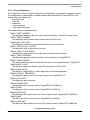
1.1 Introduction
This document describes the features of the RF Development Platform project. It is a
learning/development tool for customers that have not used Freescale’s RF solutions. It supports Tango3
(MC33493), Romeo2 (MC33591) RF modules and MC908QF4EVB at 315, 434, 868, and 928 MHz. The
design supports future RF devices like the MC33695 (Echo). Also, it is possible to add sensor boards to
demo complex systems such as RF enabled PIR detectors, smoke alarms, or fire alarms.
This development platform uses Freescale modular MCU boards and Tango3/Romeo2 RF boards to
allow the user to ‘plug and play’ any HC(S)08 MCU and any RF module. It provides Tango3/Romeo2,
keypad, LCD, relay, TRIAC, buzzer, LED software drivers, and TEAMAC encryption software in order to
reduce development time.
To date, most RF reference designs and tools have been ‘hardwired’ to a specific task. For example, RK2
RKE demo, or tire pressure monitor demo. This allows the user to get a feel of component count, PCB
size, etc., related to a very specific application. However, there are many designers developing a wide
variety of applications where the exact requirements vary from application to application.
Therefore, the RF development platform provides a general-purpose platform that allows the user to
prototype and demonstrate many different applications. It reuses forthcoming Tango3 and Romeo2
development tools to reduce development time/costs, maintain compatibility with off the shelf
development tools, and guarantee good RF performance. It is shipped pre-configured to demonstrate
RKE/remote sensing and home connectivity RF networks using the QF4, Tango3, and Romeo2.
The tool set consists of a set of MCU modules that use a common connector layout named ‘40-pin
connector’. All new HC(S)08 MCUs, and many older parts, have an evaluation board supporting this
standard. RF modules for Tango, Romeo and Echo were developed to support the same connector
standard. A set of software drivers were developed for these modules to allow users to quickly develop
application code.
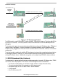
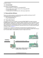
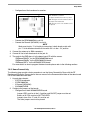
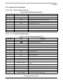
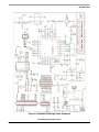
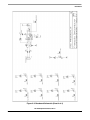
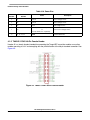
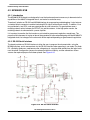
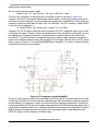
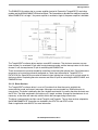
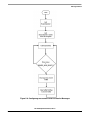
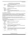
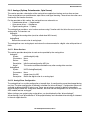
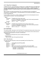
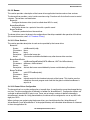
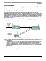
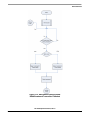
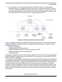
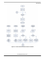
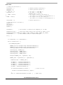
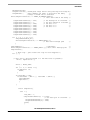
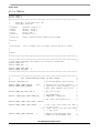
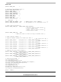
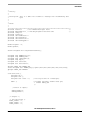
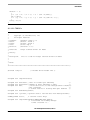
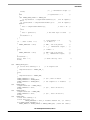
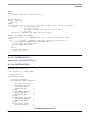
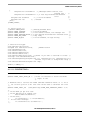
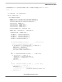
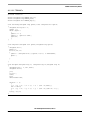
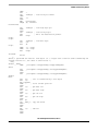
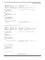
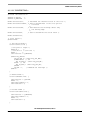
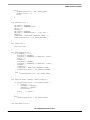
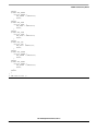
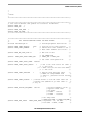
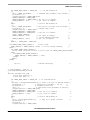
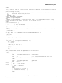
Figure 1-1 shows the RF development platform concept based on Freescale’s RF development tools. It
reuses all existing tools. Additionally, two new boards have been developed, a 68HC908QF4 board and
a general-purpose baseboard.
RF Development Platform, Rev. 0
Freescale Semiconductor
11
Introduction and Setup
USER INTERRUPTS
ANALOGS
SWITCHES
KEY PAD
SCI
USER INPUTS
POTENTIOMETER
PUSH BUTTONS
RF COMMS USING RF DRIVERS + TEAMAC
C
RF
M
OM
S
I NG
US
RF
D
ER
RIV
S+
AM
TE
AC
RF COMMS USING RF DRIVERS + TEAMAC
Figure 1-1. RF Development Platform
The QF4 board is a small PCB with QF4, some switches, LEDs and an antenna. This allows the QF4 to
be used as a transmitter. It will also provide a monitor mode interface for software development and
debugging.
The baseboard is a general-purpose interface board that features keypad, LCD display, relay, TRIAC and
various other I/O peripherals. It uses the standard I/O connector concept, so MCU modules and RF
modules can be plugged into it. Note, this means it can be used in a transmitter, receiver, or transceiver
configuration
These two boards in combination with the RF development tools provide a complete hardware platform
for developing simple RF networks. RF communications between boards can be achieved using the
existing RF software drivers. Additionally, encryption can be added using TEAMAC software routines.
1.2 RFDP Baseboard (Key Features)
The baseboard is a general-purpose interface board compound by a keypad, LCD display, relay, TRIAC
and various other I/O peripherals. The features of this development tool are listed below.
• Two female standard 40-pin I/O connectors for RF modules (Tango3, Romeo2, Echo)
• Two male standard 40-pin I/O connectors for MCU demo boards
• One power supply unit for 3-V and 5-V MCU and RF modules
• 12-key keypad
• One 2 x16 character LCD
RF Development Platform, Rev. 0
12
Freescale Semiconductor
QF4 (Key Features)
•
•
•
•
•
•
•
•
•
•
•
•
•
Two SPST switches
One op-amp for sensor signal boosting
One opto-resistor sensor
Eight LEDs
One potentiometer
One mains relay
One opto-isolated TRIAC
One buzzer
Zero-cross detection circuit
Serial monitor interface for debug and programming
Powered with a 7.5 Vac adaptor
Fuse protected
Prototyping area
1.3 QF4 (Key Features)
1.3.1 Microcontroller
The MC69HC908QF4 is a high-performance M68HC08 architecture microcontroller with an UHF
transmitter module. The main characteristics of the microcontroller are:
• High-performance M68HC08 architecture
• 4-channel, 8-bit analog-to-digital converter (ADC)
• 16-bit, 2-channel timer interface module (TIM)
• 13 general-purpose input/output (I/O) ports
• IRQ, RST, KBI, COP, and LVI capabilities
• Power saving wait and stop modes
• Trimmable internal oscillator
• Supply voltage: 2.2–3.6 V
• Temperature range: –40 to 128°C
1.3.2 UHF Transmitter Module
The main characteristics of the UHF transmitter module are:
• RF transmitter (UHF)
• 315/434/868/928 MHz operation
• OOK and FSK modulation selectable
• Adjustable output power
• Data clock output for MCU
• Fully integrated VCO
• Low external component count
• Typical application compliant with ETSI standard
• 32-pin plastic low-profile quad flat pack (case number 873A)
RF Development Platform, Rev. 0
Freescale Semiconductor
13
Introduction and Setup
1.3.3 MC908QF4EVB
Key features of the MC908QF4EVB are:
• Different frequencies available just by changing the BOM
• With and without power amplifier versions just by changing the BOM
• Low cost PCB (only two layers)
• It can be used as an evaluation board for a wide range of applications
1.4 Demonstration Software
There are two software programs for demonstrating some capabilities and features of the RF
development platform, these demo programs are:
1. RKE / Remote Sensing Demo
2. Home Connectivity Demo
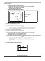
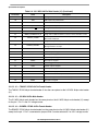
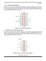
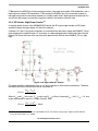
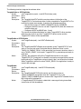
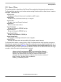
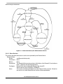
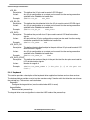
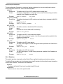
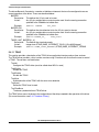
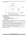
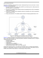
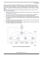
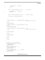
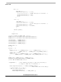
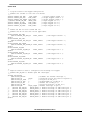
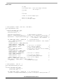
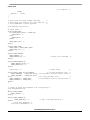
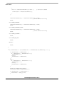
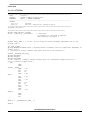
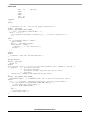
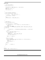
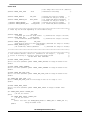
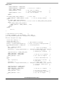
1.4.1 Home (Key Features)
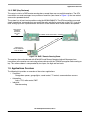
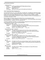
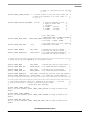
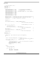
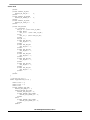
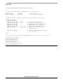
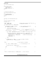
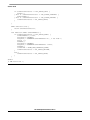
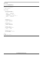
The system has at least two transmitters, one using the MC68HC908QF4, the other one using an
MC9S08RG60 MCU module with the Tango3 RF module and baseboard. The QF4 transmitter can send
simple ‘open/close’ commands that can control the relay and display some text on the LCD. It can also
take ‘analog’ input from a potentiometer and send it to a receiver when values need to be updated. The
second transmitter can also send ‘open/close’ commands and the value of a key pressed on the keypad.
This demo is shown in Figure 1-2.
The receiver has a baseboard with AP64 MCU and Romeo2 boards attached. Messages from
transmitters to the receiver are sent using software drivers with the TEAMAC encryption code running on
top. This software demo is compounded by two layers, the high and low levels.
USER INPUTS
POTENTIOMETER
PUSH BUTTONS
RF COMMS USING RF DRIVERS + TEAMAC
Figure 1-2. Simple System to Show Control of Lamps
and other Mains Powered Items
RF Development Platform, Rev. 0
14
Freescale Semiconductor
Applications Overview
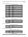
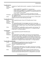
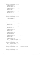
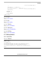
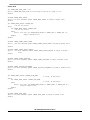
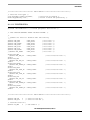
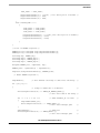
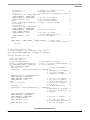
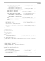
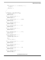
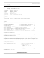
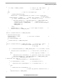
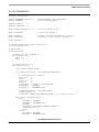
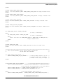
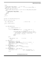
1.4.2 RKE (Key Features)
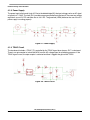
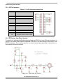
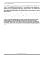
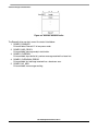
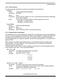
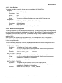
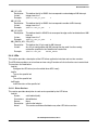
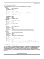
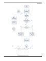
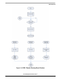
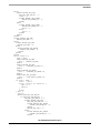
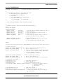
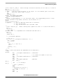
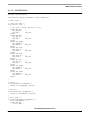
This setup is similar to RKE/remote sensing demo, except there are now multiple receivers. The QF4
transmitters can send messages to any number of receivers (two shown in Figure 1-3) that can control
some mains powered devices.
The system has at least two transmitters using the MC68HC908QF4. The QF4 transmitters can send
simple ‘open/close’ commands that can control the relay and display some text on the LCD; it can also
take ‘analog’ input from a potentiometer and send it to the receiver when values need to be updated.
USER INPUTS
ANALOGS
SWITCHES
KEY PAD
SCI
RF COMMS USING RF DRIVERS + TEAMAC
USER INPUTS
POTENTIOMETER
PUSH BUTONS
C
RF
M
OM
S
ING
US
D
RF
ER
RIV
S+
AC
AM
E
T
Figure 1-3. RKE / Remote Sensing Demo
The receivers have a baseboard with AP64 MCU and Romeo2 boards attached. Messages from
transmitters to the receiver are sent using software drivers with the TEAMAC encryption code running on
top. This software demo is compounded by two layers, the high and low levels.
1.5 Applications Overview
The following list provides an overview of the various applications:
• Consumer:
Garage door opener, garage lights, sound control, TV control, communications sensors
• Automotive:
Locks, TPS, radio control, RKE
• Industrial:
Remote sensing
RF Development Platform, Rev. 0
Freescale Semiconductor
15
Introduction and Setup
1.6 Setup Guide
1.6.1 RKE / Remote Sensing Demo
The following steps provide a basic procedure to run the RKE / Remote Sensing Demo with the RF
Development Platform.
1. Unpack demo boards:
– 2 RFDP baseboards
– 1 DEMO908AP64
– 1 DEMO9S08RG60
– 1 Tango3 (MC33493)
– 1 Romeo2 (MC33591)
– 1 MC908QF4EVB.
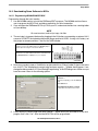
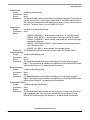
2. Configure the jumpers of the boards.
– Configuration of the DEMO9S08RG60 board:
Jumper PWR_SEL:1 must be set and PWR_SEL:2 must not be placed
Jumpers USER: 1...4 must not be placed
– Configuration of the baseboard as transmitter:
These jumpers must be set: JP1, JP4, JP5, JP6,
JP7, JP8, JP9, JP10, JP11, JP15, JP19, JP20,
JP21, JP22, JP23, JP24, and JP25.
The jumper JP30 must be in the 1–2 position.
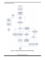
Note: This figure shows the relative location of
the jumpers in the baseboard.
Note: The gray color is “set” and white color is
“not placed”.
–
–
Connect the DEMO9S08RG60 to slot J1.
Connect the Tango3 (MC33493) to slot J2.
NOTE
Make sure that pin “1” of the 40-pin connectors in both boards matches with
pin “1” of the baseboard and that the switch S3 is in the + 3.3-V position.
–
–
Configuration of the MC908QF4EVB board:
Jumper VSEL must be in the 1–2 position, and the ON/OFF jumper must be set.
Battery of 9 V PP3 must be in the BATTHOLDER
Jumpers from J3 to J7 and J11 must be set
The other jumpers must not be placed
Configuration of the DEMO908AP64 board:
Jumper PWR_SEL:1 must be set and PWR_SEL:2 must not be placed
Jumpers OSC_SEL must be in the 2–3 position.
The other jumpers are don’t cares
RF Development Platform, Rev. 0
16
Freescale Semiconductor
Setup Guide
–
Configuration of the baseboard as receiver:
These jumpers must be set: JP14, JP17, JP18,
JP19, JP20, JP21, and JP22.
The jumper JP29 must be in the 1-2 position.
Note: The figure shows the relative location of
the jumpers in the baseboard.
Note: The gray color is “set” and white color is
“not placed”.
–
–
Connect the DEMO908AP64 to slot J3.
Connect the Romeo2 (MC33591) to slot J4.
NOTE
Make sure that pin “1” of the 40-pin connectors in both boards match with
pin “1” of the baseboard and that the switch S3 is in the + 5 V position.
3. Connect the antennas to SMA connectors.
4. Connect 9 Vac to both baseboards in the jack J6.
5. The code for the RKE demo is in the demo board CD with the names:
“RKEdemoRG60Tx” for the DEMO9S08RG60 board
“RKEdemoAP64Rx” for the DEMO908AP64 board
“RKEdemoQF4Tx” for the MC908QF4EVB board.
For more details on how to program the demo boards please refer to the following sections.
1.6.2 Home Connectivity
The following steps provide a basic procedure to run the Home Connectivity Demo with the RF
Development Platform. Please refer to the user manual in the Documentation folder of the demo board
CD for more detailed information.
1. Unpack demo boards:
– 2 RFDP baseboards
– 2 DEMO908AP64
– 2 Romeo2 (MC33591)
– 2 MC908QF4EVB.
2. Configure the jumpers of the boards.
– Configuration of both MC908QF4EVB board:
Jumper VSEL must be in the 1-2 position and ON/OFF jumper must be set.
Battery of 9V PP3 must be in BATTHOLDER.
Jumpers from J3 to J7, and J11 must be set.
The other jumpers must not be placed.
RF Development Platform, Rev. 0
Freescale Semiconductor
17
Introduction and Setup
–
–
Configuration of both DEMO908AP64 board:
Jumper PWR_SEL:1 must be set and PWR_SEL:2 must not be placed.
Jumpers OSC_SEL must be in 2-3 position.
The other jumpers are don’t cares.
Configuration of both baseboard as receiver:
These jumpers must be set: JP14, JP17, JP18,
JP19, JP20, JP21, and JP22.
The jumper JP29 must be in the 1–2 position.
Note: The figure shows the relative location of
the pins in the baseboard.
Note: The gray color is “set” and white color is
“not placed”.
3. Connect the DEMO908AP64 to slot J3.
4. Connect the Romeo2 (MC33591) to slot J4.
NOTE
Make sure that pin “1” of the 40-pin connectors in both boards matches with
pin “1” of the baseboard and that the switch S3 is in the + 5 V position.
5. Connect the antennas to SMA connectors.
6. Connect 9 Vac to both baseboards in the jack J6.
7. The code of Home Connectivity Demo is in the demo board CD with the names:
“HomedemoAP64Rx” for the DEMO908AP64 board
“HomedemoQF4Rx” for the MC908QF4EVB board
For more details regarding how to program the demo boards please refer to the following sections.
NOTE
In the code of HomedemoAP64Rx you must change the definition of
ROMEO_ID_VALUE in the file Romeo.h (61). One board of
DEMO908AP64 must be saved with the value 0x10 and the other with
0x20.
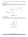
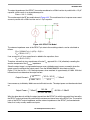
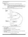
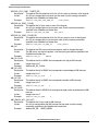
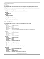
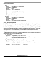
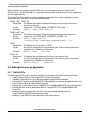
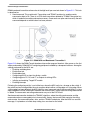
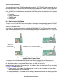
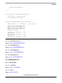
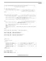
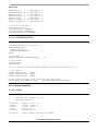
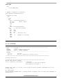
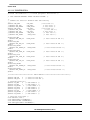
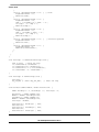
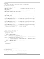
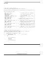
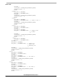
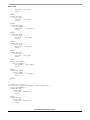
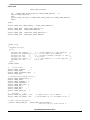
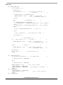
BASEBOARD
8. The lamp connection is shown in Figure 1-4.
LAMP
J7
AC LINE
Figure 1-4. Lamp Connection
RF Development Platform, Rev. 0
18
Freescale Semiconductor
Setup Guide
1.6.3 Downloading Demo Software to MCUs
1.6.3.1 Programming MC68HC908QF4 MCU
Programming through the serial monitor:
1. Use the MON08 monitor to install the RKEdemoQF4Tx program. The MON08 monitor allows a
user to program the MCU Flash and debug application via serial connection.
2. Copy and open the “RKEdemoQF4Tx.zip” file to your PC, and extract the files into a working folder
on your desktop.
NOTE
Be sure to extract, and not just copy, the files.
3. The next step is to prepare the board by plugging in the 9-V battery or connecting an external 3.3-V
source to VCONCTR and selecting the correct jumper position for VSEL. If using a 9-V battery, set
the jumper to connect positions 1 and 2 of the VSEL header.
For an external voltage source set the jumper to connect
positions 2 and 3 of the VSEL header. The ON/OFF jumper
must be placed if using the on-board 9-V battery.
In the CONFIGJMPS header, the jumpers that should be
placed are J1, J2, and J9. Next connect the serial cable from
the MC908QF4EVB to a COM port on your computer.
4. Now you are ready to open a CodeWarrior project and click on “Debug” under Project in the menu
bar, or hit F5. The “Attempting to contact target and pass security…” window should appear. If not,
change the debug mode to “In-Circuit Debug/Programming” in the PEDebug menu. Make sure you
have the same values for the following options:
Target Hardware Type: Class I
Serial Port: 1
(Could vary depending on the PC COM port
used)
Baud: 9600 Baud
Target MCU Security Bytes: “IGNORE
security failure and enter monitor mode”.
5. Finally click the “Contact target with these settings…” button and if you are asked to “Erase and
program flash” click “Yes”. After that the MCU Flash will be programmed.
RF Development Platform, Rev. 0
Freescale Semiconductor
19
Introduction and Setup
Programming using the MON08 multilink interface:
1. The next table shows the jumper settings for programming the MC908QF4EVB using the MON08
multilink interface.
It is important to verify that the VSEL and ON/OFF jumpers
have been removed, in order to avoid damage to the board or
MON08 multilink interface. Power supply for programming will
be provided by MON08 multilink. None of the jumpers shown
in 1–10 must be set.
In the CONFIGJMPS header, the jumpers that should be
placed are J2 and J10.
2. Plug the MON08 multilink to the MON08_MULTILINK connector located in the MC908QF4EVB.
Please be sure to match the red line of the MON08 multilink interface with the MON08_MULTILINK
connector. Apply power to the MON08 multilink interface and connect it to you PC parallel port.
3. Now you are ready to open a CodeWarrior project and click the “Debug” button in the menu bar
under the project window, or hit F5. The “Attempting to contact target and pass security…” window
should appear. If not, change the debug mode to “In-Circuit Debug/Programming” in the PEDebug
menu. Make sure you have the same values for the following options:
Target Hardware Type: Class VII
LPTx: Parallel Port x
(Could vary depending on the PC Parallel
port used)
Device Type: QY
Device Power: 3 Volts, provided by P&E
Interface
Device Clock: 4.9152 MHz, provided by
P&E Interface Pin13
Clock Divider: 2
Target MCU Security Bytes: “IGNORE
security failure and enter monitor mode”.
4. Finally click the “Contact target with these settings…” button and if you are asked to “Erase and
program Flash” click “Yes”. After that the MCU Flash will be programmed.
RF Development Platform, Rev. 0
20
Freescale Semiconductor
Setup Guide
1.6.3.2 Programming RG60MCU
The following procedure shows how to load code into the demo board using the serial monitor program
that resides in the MC9S08RG60’s Flash memory.
1. Before running this demo, please install CodeWarrior for HCS08 Release 3.0 or higher on your PC.
Also, please copy the RKEdemoRG60Tx.zip file from the demo board CD to your PC and extract
the files into a working folder. The RKEdemoRG60Tx.zip file can be found on the demo board CD
in the Documentation directory.
2. Connect a straight-through DB-9 serial cable between COM1 on the PC and the SCI1 connector
(DB9 connector) on the demo board. If you are using a different PC COM port, you will need to
adjust the settings within the CodeWarrior IDE.
3. Navigate to the working folder and double click the RKEdemoRG60Tx.mcp project. The
CodeWarrior IDE will launch.
4. Hold SW1 low while turning the power supply ON. Then release SW1. (If power is already applied,
press the reset switch and SW1 simultaneously. Release the reset switch and then release SW1.)
5. Double click on the main.c file in the Sources folder in the project window.
6. Select Debug from the Project menu, or press F5, or click the green arrow on the CodeWarrior tool
bar. The True-Time Simulator & Real-Time Debugger initiates serial communications with the
demo board. The demo code is erased and re-programmed in the MC9S08RG60’s Flash memory.
The serial monitor code is not erased. (If the debugger is launched when the board is not powered,
you will see a series of error notifications. Cancel and close these messages; close the debugger
window; and go back to step 4.)
7. Disconnect the serial cable from the demo board.
The serial monitor can be used for much more than just programming new code without requiring a
special debug pod. Many debug operations (memory modifies breakpoints, real-time bug traces, etc.) can
also be run over the serial cable while in this mode. Refer to application note AN2140 for more information
on the serial monitor.
1.6.3.3 Programming AP64MCU
1. Use the MON08 monitor to install RKEdemoAP64Rx program. The MON08 monitor allows a user
to program the MCU Flash and debug application via serial connection.
2. Copy and open the “RKEdemoAP64Rx.zip” file to your PC, and extract the files into a working
folder on your desktop.
NOTE
Be sure to extract, and not just copy, the files.
3. If you have not already done so, connect serial cable and apply power to the board.
4. In the working folder on the desktop, double click on the “RKEdemoAP64Rx.mcp” project file. The
CodeWarrior IDE will launch.
5. Open “RKEdemoAP64Rx.c” in the source folder by double clicking on it.
6. Please change the jumpers on the board to ensure proper communication between the PC and
DEMO908AP64 board.
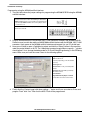
Figure 1-5. MON08 Debug Setting for Serial Connection
RF Development Platform, Rev. 0
Freescale Semiconductor
21
Introduction and Setup
7. Click on “Debug” under Project in the menu bar or hit “F5.” The True-Time Simulator & Real-Time
Debugger interface window will appear. The “Attempting to contact target and pass security…”
window should appear. Please make sure the following options are configured correctly:
– Target Hardware Type: Class 3
– Serial Port: 1 (Depends on the PC COM Port)
– Baud: 9600 Baud
– Target MCU Security bytes: Check the “IGNORE security failure and enter monitor mode”
checkbox.
8. Click the “Contact target with these settings…” button and follow the instructions on the screen.
When the “Erase and Program Flash?” window appears, click the “Yes” button.
9. To cycle the power, you should remove the VR1 jumper (PWR_SEL port) and reinstall the VR1
jumper (PWR_SEL). This action has turned the MCU supply power off and on. The + 5-V LED will
stay on during this power cycle. Click “OK” in the “Power Cycle Dialog” window.
10. The “CPROG08SZ Programmer” window should close after the MCU Flash is programmed. You
are now ready to run the DEMO908AP64_ATD code.
1.6.3.4 Operating the RKE / Remote Sensing Demo
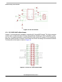
This demo is compounded by two transmitters and one receiver. When the push button one ‘PS1’ is
pressed on the MC908QF4EVB the ‘open’ command is sent over the RF link. If push button two ‘PS2’ is
pressed the ‘close’ command is sent. The red LED ‘LED1’ turns on every time one of these buttons has
been pressed. The green ‘LED2’ will turn on every time the potentiometer is set to a different level. This
indicates that the value present on the ADC channel has been updated and sent over the RF link.
As a result of moving the switch ‘S2’ from position one to position two on the Tx2 (MCU-RG60 and Tango3
attached to the baseboard) an ‘open’ command is sent. If the ‘S2’ switch is moved from position 2 to
position 1 a ‘closed’ command is sent. The Tx2 can also send the value of the key pressed on the keypad,
every time a key is pressed its value will be sent to over the RF link.
The receiver will show the relay status, the analog value, rolling counter, MAC as well as the key pressed
on the RG60-Tango3 transmitter.
1.6.3.5 Operating the Home Connectivity Demo
Both transmitters have the same functionality. Both transmitters can send ‘open’, ‘close’ commands, send
the potentiometer value and select which receiver will be enabled to execute commands or update values.
When the push button one ‘PS1’ is pressed on the transmitters the ‘open’ command is sent over the RF
link. If push button two ‘PS2’ is pressed the ‘close’ command is sent. The red ‘LED1’ turns on every time
one of these buttons has been pressed. The green ‘LED2’ will turn on every time the potentiometer is set
to a different level. This indicates that the value present on the ADC channel has been updated and sent
over the RF link.
Transmitters enter to ‘select receiver’ mode when ‘PS1’ and ‘PS2’ are simultaneously pressed, the ‘LED1’
and ‘LED2’ will turn on indicating this state. The transmitter will remain on this state for three seconds, if
any push button has not been pressed during this time the Tx will enable both receivers for executing the
sent commands. Pressing push button one before this time expires, it will select Rx1; pressing push
button two will select Rx2.
RF Development Platform, Rev. 0
22
Freescale Semiconductor
Chapter 2
Operational Description
2.1 Introduction
The RF development platform provides a general-purpose platform that allows the user to prototype and
demonstrates many different applications. It reuses the Tango3 and Romeo2 development tools reducing
development time/costs and maintaining compatibility with off the shelf development tools.
This section describes the electrical characteristics, user interfaces, and connections for the RF
Development Platform.
2.2 Baseboard
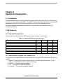
2.2.1 Electrical Characteristics
The baseboard must be fed with an AC/AC power adaptor, typically 7.5 Vac output.
Table 2-1. Baseboard Electrical Characteristics
Min
Typ
Max
Unit
AC input voltage
Inputs/Outputs
7
7.5
8
Vac
AC current consumption
50
150
—
mA
Triac voltage (J9)
—
—
300
Vac
Triac current (J9)
—
—
2
A
Relay voltage (J7)
—
—
250
Vac
Relay current (J7)
—
—
2
A
Input voltage signal booster (J8)
—
—
3
VPP
2.2.2 User Interfaces (Keypad, LCD, Jumpers, etc.)
The baseboard user interface consists of one keypad, one LCD, one buzzer, one potentiometer and two
switches.
• Keypad — A keypad with 12 keys, number from ‘0’ to ‘9’ and the special characters ‘#’ and ‘*’.
• LCD — A 16 characters per 2 lines liquid crystal display
• BUZZER — A buzzer for general propose
• POT — Potentiometer for general propose
• S1 and S2 — Two switches for general propose
RF Development Platform, Rev. 0
Freescale Semiconductor
23
Operational Description
2.2.2.1 Jumper Description
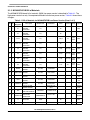
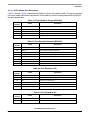
Table 2-2 provides a functional description of each jumper located in the baseboard.
Table 2-2. Baseboard Jumper Descriptions
Jumper
Name
Functional Description
JP1
Connects the switch 2 (S2) to pin 37 (SW2) of the 40-pin connectors
JP2
Connects the TxD RS-232 interface to pin 5 (TXD) of the 40-pin connectors
JP3
Connects the RxD RS-232 interface to pin 7 (RXD) of the 40-pin connectors
JP4
Connects the keypad row 1 to pin 40 (ROW1) of the 40-pin connectors
JP5
Connects the keypad row 2 to pin 31 (ROW2) of the 40-pin connectors
JP6
Connects the keypad row 3 to pin 33 (ROW3) of the 40-pin connectors
JP7
Connects the keypad row 4 to pin 36 (ROW4) of the 40-pin connectors
JP8
Connects the keypad column 1 to pin 30 (COL1) of the 40-pin connectors
JP9
Connects the keypad column 2 to pin 35 (COL2) of the 40-pin connectors
JP10
Connects the keypad column 3 to pin 32 (COL3) of the 40-pin connectors
JP11
Connects the keypad interrupt signal to pin 2 (IRQ) of the 40-pin connectors
JP12
Connects the T2IN to R2OUT pins of the RS-232 transceiver (IC1)
JP13
Connects the buzzer to pin 39 (BUZ/LED8) of the 40-pin connectors
JP14
Connects the zero-cross detection to pin 9 (KBI) of the 40-pin connectors
JP15
Connects the switch 1 (S1) to pin 26 (CAN/LIN_TX/SW1) of the 40-pin connectors
JP16
Connects the opto-sensor to pin 22 (OPTO_SENSOR) of the 40-pin connectors
JP17
Connects the TRIAC to pin 34 (TRIAC) of the 40-pin connectors
JP18
Connects the relay to pin 29 (RELAY) of the 40-pin connectors
JP19
Connects the LED 1 to pin 28 (CAN/LIN_RX/LED1) of the 40-pin connectors
JP20
Connects the LED 2 to pin 6 (LED2) of the 40-pin connectors
JP21
Connects the LED 3 to pin 8 (LED3) of the 40-pin connectors
JP22
Connects the LED 4 to the LED4 trace (pin 3 JP30, pin 1 JP31)
JP23
Connects the LED 5 to pin 19 (LED5/MISO) of the 40-pin connectors
JP24
Connects the LED 6 to pin 21 (LED6/SCLK) of the 40-pin connectors
JP25
Connects the LED 7 to pin 23 (LED7/SS) of the 40-pin connectors
JP26
Connects the LED 8 to pin 1 of the JP32
JP27
Connects the OpAmp out to pin 18 (OPAMP_SENSOR) of the 40-pin connectors
JP28
Connects the potentiometer to pin 20 (POT) of the 40-pin connectors
JP29
Placed in position 1-2 for use of 5 V or in position 2–3 for use of 3.3-V in 40-pin connector (ROMEO/ECHO: J4)
JP30
Placed in position 1–2 connects the pin 15 (DATA_T) of the J1 & J2 40-pin connectors to the pin 15 (TCH1) of the
J3 and J4 40-pin connectors.
Placed in position 2–3 connects the pin 15 (TCH1) of the J3 & J4 40-pin connectors to the LED4 trace (pin 1 JP22,
pin 1 JP31).
JP31
Connects the pin 17 (MOSI) of the 40-pin connectors to the LED4 trace (pin 1 JP22, pin 3 JP30)
JP32
Placed in position 1–2 connects the LED8 trace (pin 1 JP26) to the pin 39 (BUZ/LED8) of the 40-pin connectors.
Placed in position 2–3 connects the buzzer to the pin 39 (BUZ/LED8) of the 40-pin connectors.
RF Development Platform, Rev. 0
24
Freescale Semiconductor
Baseboard
2.2.3 Connector Pin Descriptions
2.2.3.1 SCI1 — RS-232 Interface Connector
Table 2-3. RS-232 DB-9 Connector (SCI1)
Pin Number
Name
Description
1
CD
Bridged with pins 4 and 6
2
RxD
Data received by the PC from the control board
3
TxD
Data transmitted from the PC to the control board
4
DTR
Bridged with pins 1 and 6
5
GND
Common ground reference
6
DSR
Bridged with pins 1 and 4
7
RTS
Optional handshake signal
8
CTS
Optional handshake signal
9
Unused
N/A
2.2.3.2 J1 — 3.3-V MCU 40-Pin Male Header
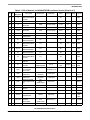
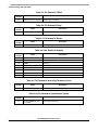
Table 2-4. 3.3-V MCU 40-Pin Male Header (J1)
Pin Number
Name
Description
1
+3.3V
2
IRQ
External interrupt request pin
3
GND
Ground reference
4
RESET
5
TXD
Transmit data of SCI
6
LED2
Yellow LED turn on/off pin
7
RXD
Receive data of SCI
8
LED3
Orange LED turn on/off pin
9
KBI
Keyboard Interrupt pin
10
D4
Data pin for LCD interface
11
ENABLE_T/STROBE_R
12
D5
13
DATACLK_T/AGC_R
14
D6
15
DATA_T
16
D7
17
MOSI
18
OPAMP_SENSOR
3.3-V voltage source
MCU reset pin
Tango standby/on control. Romeo strobe oscillator control.
Data pin for LCD interface
Tango clock available for the MCU. Romeo AGC modulation
selection.
Data pin for LCD interface
Tango data input.
Data pin for LCD interface
Master out/slave in pin of SPI
ADC input from signal boosting circuitry
RF Development Platform, Rev. 0
Freescale Semiconductor
25
Operational Description
Table 2-4. 3.3-V MCU 40-Pin Male Header (J1) (Continued)
Pin Number
Name
Description
19
LED5/MISO
20
POT
21
LED6/SCLK
22
OPTO_SENSOR
23
LED7 / SS
24
E
25
MODE_T/ENABLELNA_R
26
CAN/LIN_TX/SW1
Transmit pin of CAN interface. Transmit pin of LIN interface.
On/off switch input pin.
27
ENABLEPA_T/RESETB
Tango enable power amplifier. Romeo SPI mode selection.
28
CAN/LIN_RX/LED1
Receive pin of CAN interface. Receive pin of LIN interface.
Orange LED turn on/off pin
29
RELAY
Relay control pin
30
COL1
Column 1 pin for keypad
31
ROW2
Row 2 pin for keypad
32
COL3
Column 3 pin for keypad
33
ROW3
Row 3 pin for keypad
34
TRIAC
TRIAC trigger control pin.
35
COL2
Column 2 pin for keypad
36
ROW4
Row 4 pin for keypad
37
SW2
On/off switch input pin
38
RS
Data or instruction select pin for LCD interface
39
BUZ/LED8
Buzzer control pin. Yellow LED turn on/off pin
40
ROW1
Orange LED turn on/off pin. Master in/slave out pin of SPI
ADC input from potentiometer
Yellow LED turn on/off pin. Serial clock pin of SPI
ADC input from opto-resistor
Orange LED turn on/off pin. Slave select pin of SPI
Enable pin for LCD interface
Tango FSF or OOK modulation selection. Romeo LNA bias control.
Row 1pin for keypad
2.2.3.3 J2 — TANGO / ECHO 40-Pin Female Header
The TANGO / ECHO 40-pin female header J2 has the same pinout as the 3-V MCU 40-pin male header
(J1).
2.2.3.4 J3 — 5V MCU 40-Pin Male Header
The 5-V MCU 40-pin male header has the same pinout as the 3-V MCU 40-pin male header (J1) except
for the pin 1. Pin 1 is the 5-V voltage source.
2.2.3.5 J4 — ROMEO / ECHO 40-Pin Female Header
The ROMEO / ECHO 40-pin female header has the same pinout as the 3-V MCU 40-pin male header (J1)
except for the pin 1. Pin 1 is connected to jumper JP29. It can be selected 5-V or 3.3-V voltage source.
RF Development Platform, Rev. 0
26
Freescale Semiconductor
Baseboard
2.2.3.6 J5 — LCD Connector
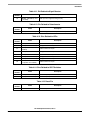
Table 2-5. LCD Connector (J5)
Pin Number
Name
1
VSS
Description
GND — ground reference
2
VDD
LCD contrast
3
Vo
Ground reference
4
RS
MCU reset pin
5
R/W
6
E
7
D0
Data bus pin 0. Not connected.
8
D1
Data bus pin 1. Not connected.
9
D2
Data bus pin 2. Not connected.
10
D3
Data bus pin 3. Not connected.
11
D4
Data bus pin 4
12
D5
Data bus pin 5
13
D6
Data bus pin 6
14
D7
Data bus pin 7
15
A
Backlight anode
16
K
Backlight cathode
Data read/write. Tied to GND (write)
Enable
2.2.3.7 J6 — AC Jack
Table 2-6. AC Jack (J6)
Pin Number
Name
Description
1
AC1
7.5 AC
2
AC2
7.5 AC
3
—
Bridged with pin 2
2.2.3.8 J7 — Relay Connector
Table 2-7. Relay Connector (J7)
Pin Number
Name
1
Line
I/O pin signal
Description
2
Load
I/O pin signal
2.2.3.9 J8 — Signal Booster Connector
Table 2-8. Signal Booster Connector (J8)
Pin Number
Name
Description
1
Positive
Positive differential input
2
Negative
Negative differential input
RF Development Platform, Rev. 0
Freescale Semiconductor
27
Operational Description
2.2.3.10 J9 — TRIAC connector
Table 2-9. Triac Connector (J9)
Pin Number
Name
Description
1
Load
I/O pin signal
2
Line
I/O pin signal
2.3 MC68HC908QF4
2.3.1 Electrical Characteristics
Table 2-10. MC68HC908QF4 Electrical Characteristics
Inputs/Outputs
Min
Typ
Max
Units
DC battery supply voltage
8
9
12
Vdc
DC external voltage
3
3.3
3.6
Vdc
Minimum logic 1 input voltage
2.1
—
—
Vdc
Maximum logic 0 input voltage
—
—
0.9
Vdc
Antenna Impedance
—
50
—
—
Board current consumption
—
11.8
35
mA
RS-232 connection speed
—
9600
—
Baud
2.3.2 User Interfaces (Keypad, LCD, Jumpers, etc.)
The MC908QF4 EVB user interface consists of two light-emitting diodes (LEDs), one potentiometer, and
two push buttons.
• SW1 is a push button located in the bottom left corner next to the battery holder. It is used to send
close commands and to select the receiver. This function depends on the demo software loaded
to the QF4 MCU.
• SW2 is a push button located next to the SW1; it is used to send open commands and to select the
receiver. This function depends on the demo software loaded to the QF4 MCU.
• LED1 is a green-light emitting diode located in the bottom left corner next to the battery holder and
below the two push buttons. It is used to indicate a reading on the potentiometer value and the
transmission of this value over the RF link.
• LED2 is a red-light emitting diode located next to the LED1. It is used to indicate a transmission of
the ‘open/close’ commands.
• R21 is a potentiometer located next to the battery holder in the left side of the MC908QF4 EVM. It
is used to change the analog value present on the ADC module.
RF Development Platform, Rev. 0
28
Freescale Semiconductor
MC68HC908QF4
2.3.2.1 Jumper Description
Table 2-11 provides a functional description of each jumper located in the MC908QF4 EVB
Table 2-11. MC908QF4EVB Jumper Descriptions
Jumper
Name
Functional Description
J1
Connects the 9.8304 MHz external oscillator to PTA5.
J2
Connects PTA0 to the RS-232 serial data line.
J3
Set this jumper to enable pushbutton SW1, it connects SW1 to
PTA0.
J4
Set this jumper to enable pushbutton SW2, it connects SW2 to
PTA3.
J5
Set this jumper to connect the potentiometer to PTA5.
J6
Set this jumper to enable LED2, it connects LED2 to PTA4.
J7
Set this jumper to enable LED1, it connects LED1 to PTB3.
J8
Connects PTB2 to the 40-pin connector.
J9
Connects PTA2 to VTST, the voltage necessary to program the Flash
through serial monitor.
J10
Connects PTA2 to the multilink high-voltage pin. It also connects
PTA2 to the 40-pin connector.
J11
Connects PTB2 to the Enable_PA pin, which enables or disables
the RF power amplifier. If this jumper is set, and the output of PTB2
is high, the power amplifier is enabled. Otherwise, the power
amplifier is disabled.
VSEL
Set jumper in position 1–2 for use with on board 9-V battery. For use
with an external 3.3-V voltage source, set jumper in position 2–3.
ON/OFF
When not using the board, take off this jumper to avoid discharging
the 9-V on-board battery. This jumper has no effect when using an
external 3.3-V voltage source connected to VCONCTR.
RF Development Platform, Rev. 0
Freescale Semiconductor
29
Operational Description
2.3.3 Connector Pin Descriptions
Table 2-12. External Connector Voltage
Pin Number
Name
1
GND
Common ground reference
Description
2
VCC
External 3.3-V supply voltage
Table 2-13. MON08 (Multilink Connector)
Pin Number(1)
Name
2
GND
6
PTA2_EX
Description
Common ground reference
High-voltage for programming (VTST)
8
PTA0
Dedicated pin for serial communication
13
PTA5
External clock
15
VCC
Supply voltage
NOTES:
1. Unused pins are not mentioned.
Table 2-14. RS-232 Serial Interface DB-9 Connector
Pin Number
Name
1
Unused
2
Serial_Out
3
Serial_In
Description
N/A
Data transmitted from the board to the PC
Data received by the board from the PC
4
DTR
Enables/disables VMCU power in the board
5
GND
Common ground reference
6
Unused
N/A
7
Unused
N/A
8
Unused
N/A
9
Unused
N/A
Table 2-15. 40-Pin Connector
Pin Number(1)
Name
1
VMCU
2
PTA2_EX
3
GND
N/A
Description
N/A
If J10 is placed, this pin connects to PTA2
9
PTA3
N/A
10
PTB4
N/A
12
PTB5
N/A
13
PTA0
N/A
14
PTB6
N/A
16
PTB7
N/A
18
PTA5
N/A
24
PTA4
N/A
38
PTB3
40
PTB2_IO
N/A
If J8 is placed, this pin connects to PTB2
RF Development Platform, Rev. 0
30
Freescale Semiconductor
Chapter 3
Schematics and Bill of Materials
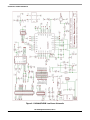
3.1 MC908QF4 EVB
3.1.1 MC908QF4 EVB Schematic Diagrams
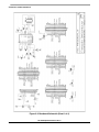
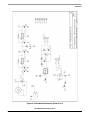
The schematics for the MC908QF4EVB board appear in Figure 3-1 and Figure 3-2. The schematic in
Figure 3-2 is for the high-power version of the board.
RF Development Platform, Rev. 0
Freescale Semiconductor
31
Schematics and Bill of Materials
Figure 3-1. MC908QF4EVB Low-Power Schematic
RF Development Platform, Rev. 0
32
Freescale Semiconductor
MC908QF4 EVB
Figure 3-2. MC908QF4EVB High-Power Schematic
RF Development Platform, Rev. 0
Freescale Semiconductor
33
Schematics and Bill of Materials
3.1.2 MC908QF4 EVB Bill of Materials
The MC908QF4EVB board bill of materials (BOM) low-power version is described in Table 3-1. The
high-power version has only 14 components different from the low-power version, Table 3-2 shows those
changes.
Table 3-1. Bill of Materials for MC908QF4EVB Low-Power Version (Sheet 1 of 3)
Item Qty
Reference
Designator
Description
Manufacturer
Part Number
Value
Tolerance Rating Footprint
1
1
C1
0603 SIZE SMT
CERAMIC
CAPACITOR
Any
NP
2
1
C2
0603 SIZE SMT
CERAMIC
CAPACITOR
Any
NP
3
2
C3 C4
0603 SIZE SMT
CERAMIC
CAPACITOR
Any
100 pF
4
3
C5 C7 C9
0603 SIZE SMT
CERAMIC
CAPACITOR
Any
NP
5
1
C6
0603 SIZE SMT
CERAMIC
CAPACITOR
Any
10 pF
±0.25 pF
50 V
NPO
0603
6
1
C8
0603 SIZE SMT
CERAMIC
CAPACITOR
Any
5.6 pF
±0.25 pF
50 V
NPO
0603
7
1
C10
0603 SIZE SMT
CERAMIC
CAPACITOR
Any
15 pF
±0.25 pF
50 V
NPO
0603
8
1
C11
0603 SIZE SMT
CERAMIC
CAPACITOR
Any
22 nF
10%
25 V
X7R
0603
9
1
MON08
2 BY 08 .10" PITCH
HEADER
SULLINS
PZC08DAAN
HEADER
2X8
10
1
CONFIGJMPS
2 BY 11 .10" PITCH
HEADER
SULLINS
PZC11DAAN
HEADER
2X11
11
1
ON/OFF
1 BY 2 .10" PITCH
HEADER
SULLINS
PZC02SAAN
HEADER
1X2
12
1
VSEL
1 BY 3 .10" PITCH
HEADER
SULLINS
PZC03SAAN
HEADER
1X3
13
1
VCONCTR
1 BY 2 .10" PITCH
HEADER
SULLINS
PZC02SAAN
HEADER
1X2
14
1
40PIN
2 BY 20 .10" SMD
FEMALE HEADER
SAMTEC
SSM-120-L-DVBE-K
HEADER
2X20
15
1
DB9
AMPHENOL
617-C009S-AJ120
DB9
16
1
JOHNSON
COMPONENTS
142-0711-821
SMANARROW
17
1
or
PBC MOUNT RIGHT
ANGLE DB9 FEMALE
0.062 NARROW EDGE
SMA
MOUNT SMA
CONNECTOR
CONNECTOR
L1
0603 SIZE CHIP
INDUCTOR
TOKO
NP
0603
5%
50 V
NPO
0603
0603
0603
LEAD FREE VERSION
RF Development Platform, Rev. 0
34
Freescale Semiconductor
MC908QF4 EVB
Table 3-1. Bill of Materials for MC908QF4EVB Low-Power Version (Sheet 2 of 3)
Item Qty
18
19
Reference
Designator
Manufacturer
L2
0603 SURFACE
MOUNT ZERO OHM
JUMPER
or
LEAD FREE VERSION
1
L3
0603 SIZE CHIP
INDUCTOR
1
or
20
Description
1
Value
Tolerance Rating Footprint
0Ω
TOKO
LEAD FREE VERSION
L4/R2
Part Number
0603 SIZE CHIP
INDUCTOR
LEAD FREE VERSION
21
1
Q1
WIDEBAND NPN
TRANSISTOR
22
1
R1
23
1
24
47 nH
5%
0603
100 nH
5%
0603
LL1608-FSL47NJ
TOKO
or
LL1608-FS47NJ
0603
LL1608-FSR10J
LL1608-FSLR10J
PHILIPS
NP
SOT23
0603 SURFACE
MOUNT RESISTOR
Any
NP
0603
R3
0603 SURFACE
MOUNT ZERO OHM
JUMPER
Any
0Ω
2
R4, R7
0603 SURFACE
MOUNT RESISTOR
Any
NP
0603
25
1
R5
0603 SURFACE
MOUNT RESISTOR
Any
15 k
0603
26
1
R6
0603 SURFACE
MOUNT ZERO OHM
JUMPER
Any
0Ω
0603
27
1
U1
UHF TRANSMITTER
AND MCU
FREESCALE
MC68HC908QF4
28
1
X1
SMT QUARTZ
CRYSTAL
CRYSTEK
CORPORATION
017113
29
1
PCB1
.062" DOUBLE SIDED
FR-4 PRINTED
CIRCUIT BD
30
1
LED1
HEWLETT-PACKARD
HSMS-C650
HEWLETT
PACKARD
HSMS-C650
3.20 x
1.60 mm
31
1
LED2
HEWLETT-PACKARD
HSMG-C650
HEWLETT
PACKARD
HSMG-C650
3.20 x
1.60 mm
32
2
D1 D2
SCHOTTKY DIODE
(HIGH-SPEED & LOW
VF)
ON
SEMICONDUCTOR
BAT54XV2T1
SOD523
33
1
D3
1A DIODE RECTIFIER
DIODES INC.
S1ABDICT-ND
SMB
SQUARE TYPE TACT
SWITCH
ALPS
SKHMPUE010
CUSTOM
ALPHA (TAIWAN)
317-2090-100K
MAXIM
ON
SEMICONDUCTOR
34
2
SW1, SW2
35
1
R21
36
1
RS-232
37
1
MC33269
or
5%
1/16 Ω
0603
LQFP
9.843750
MHz
±30 ppm
CL
18 pF
HC49S
SMD
MC908QF4 rev B
POTENTIOMETER
RS-232
TRANSCEIVER
3.3V LOW DROPOUT
VOLTAGE
REGULATOR
LEAD FREE VERSION
0.1 Ω
CUSTOM
MAX3232E
3.3 V
16 WIDE
.300"
SOIC
MC33269DT-3.3
3.3 V
CUSTOM
100 k
20%
MC33269DT-3.3G
RF Development Platform, Rev. 0
Freescale Semiconductor
35
Schematics and Bill of Materials
Table 3-1. Bill of Materials for MC908QF4EVB Low-Power Version (Sheet 3 of 3)
Item Qty
Reference
Designator
Description
Manufacturer
Part Number
PLASTIC 9V BATTERY
HOLDER
KEYSTONE
ELECTRONICS
1294
CUSTOM
ON
SEMICONDUCTOR
BC80740LT1
SOT23
38
1
BATTHOLDER
39
1
Q2
PNP GENERAL
PURPOSE
TRANSISTOR
or
LEAD FREE VERSION
40
1
C12
VERTICAL
ELECTROLYTIC
CAPACITOR
41
6
42
1
43
Value
Tolerance Rating Footprint
BC80740LT1G
ELNA
RV2-16V470M-R
47 µF
16 V
CUSTOM
0805 SIZE SMT
C13, C14, C15,
CERAMIC
C16, C17, C18
CAPACITOR
Any
0.1 µF
10%
50 V
X7R
0805
C19
0603 SIZE SMT
CERAMIC
CAPACITOR
Any
22 nF
10%
25 V
X7R
0603
1
R8
0603 SURFACE
MOUNT RESISTOR
Any
120 Ω
5%
1/16 Ω
0603
44
1
R9
0603 SURFACE
MOUNT RESISTOR
Any
150 Ω
5%
1/16 Ω
0603
45
6
R10, R11, R16, 0603 SURFACE
R17, R18, R19 MOUNT RESISTOR
Any
10 k
5%
1/16 Ω
0603
46
1
R15
0603 SURFACE
MOUNT RESISTOR
Any
47 k
5%
1/16 Ω
0603
47
1
R13
0603 SURFACE
MOUNT RESISTOR
Any
2.2 k
5%
1/16 Ω
0603
48
3
R12, R14, R20
0603 SURFACE
MOUNT RESISTOR
Any
1k
5%
1/16 Ω
0603
49
1
OSC
SMD OSCILLATOR
CITIZEN
CMX-309FB
3.3 V
CUSTOM
50
1
ANTENNA
NEARSON
L324AM-315S
51
2
STANDOFFS
KEYSTONE
ELECTRONICS
2202
52
10
JUMPERS
SULLINS
SSC02SYAN
NDK SPEC
EXS10B-00846
REF LN-G102-950
CL
12pF
NDKNX8045
FOR X1 PLEASE USE IF
AVAILABLE:
SMT QUARTZ
CRYSTAL
9.830
MHz
9.84375
MHz
±50 ppm
"NP" IN VALUE FIELD INDICATES COMPONENT POSITION NOT POPULATED
PLEASE USE LEAD FREE VERSIONS WHERE POSSIBLE
RF Development Platform, Rev. 0
36
Freescale Semiconductor
Baseboard
Table 3-2. Bill of Material Changes for High-Power Version
Item Qty
Reference
Designator
Description
Manufacturer
Part Number
Value
Tolerance Rating Footprint
1
1
C1
0603 SIZE SMT
CERAMIC
CAPACITOR
Any
10 nF
10%
25 V
X7R
0603
2
1
C2
0603 SIZE SMT
CERAMIC
CAPACITOR
Any
100 pF
5%
50 V
NPO
0603
3
1
C4
0603 SIZE SMT
CERAMIC
CAPACITOR
Any
47 pF
5%
50 V
NPO
0603
4
1
C7
0603 SIZE SMT
CERAMIC
CAPACITOR
Any
6.8 pF
±0.25 pF
50 V
NPO
0603
5
1
C8
0603 SIZE SMT
CERAMIC
CAPACITOR
Any
10 pF
±0.25 pF
50 V
NPO
0603
6
1
C9
0603 SIZE SMT
CERAMIC
CAPACITOR
Any
10 pF
± .25 pF
50 V
NPO
0603
7
1
C10
0603 SIZE SMT
CERAMIC
CAPACITOR
Any
5.6 pF
7
1
C10
8
1
L1
0603 SIZE CHIP
INDUCTOR
TOKO
68 H
17
1
L1
or
LEAD FREE VERSION
1
L2
0603 SIZE CHIP
INDUCTOR
9
or
10
11
LL1608-FSL68NJ
TOKO
LEAD FREE VERSION
L3
0603 SIZE CHIP
INDUCTOR
or
LEAD FREE VERSION
1
L4/R2
0603 SIZE CHIP
INDUCTOR
1
or
LL1608-FS68NJ
LL1608-FS56NJ
or
56 nH
18
LL1608-FSL56NJ
TOKO
LL1608-FS47NJ
LEAD FREE VERSION
LL1608-FS56NJ
L2
or
47 nH
19
LL1608-FSL47NJ
TOKO
1
1
L3
or
56 nH
20
LL1608-FSL56NJ
1
L4/R2
or
12
1
Q1
WIDEBAND NPN
TRANSISTOR
13
1
R1
0603 SURFACE
MOUNT RESISTOR
Any
10 k
5%
1/16Ω
0603
14
1
R3
0603 SURFACE
MOUNT RESISTOR
Any
1.8 k
5%
1/16Ω
0603
PHILIPS
BFR92A
5 GHz
SOT23
3.2 Baseboard
3.2.1 Baseboard Schematics
The schematic diagram of the baseboard is shown in Figure 3-3.
RF Development Platform, Rev. 0
Freescale Semiconductor
37
Schematics and Bill of Materials
Figure 3-3. Baseboard Schematic (Sheet 1 of 4)
RF Development Platform, Rev. 0
38
Freescale Semiconductor
Baseboard
Figure 3-3. Baseboard Schematic (Sheet 2 of 4)
RF Development Platform, Rev. 0
Freescale Semiconductor
39
Schematics and Bill of Materials
Figure 3-3. Baseboard Schematic (Sheet 3 of 4)
RF Development Platform, Rev. 0
40
Freescale Semiconductor
Baseboard
Figure 3-3. Baseboard Schematic (Sheet 4 of 4)
RF Development Platform, Rev. 0
Freescale Semiconductor
41
Schematics and Bill of Materials
3.2.2 Baseboard Bill of Materials
The baseboard bill of materials is shown in
Table 3-3. Bill of Materials for the Baseboard (Sheet 1 of 2)
Item Qty.
Designator
Description
Manufacturer
Part Number
Maxim
MAX3232E
5.0-V Regulator
National
LP8340CDT-5.0
IC3
3.3-V Regulator
National
LP8340CDT-3.3
1
IC4
OpAmp
1
IC5
OptoIsolator
1
1
IC1
IC Transceiver 5 V
2
1
IC2
3
1
4
5
6
12
7
4
R6, R8, R21, R35
8
1
On
MC33502-D
Fairchild
MOC3023M
Panasonic – ECG
ERJ6ENF1002V
1 K 1 % Resistor
Panasonic – ECG
ERJ6ENF1001V
R26
6.81 KΩ 1 % Resistor
Panasonic – ECG
ERJ6ENF6811V
R1, R5, R3, R9–R14,
10 K 1 % Resistor
R15,R16, R23
9
1
R17
221 Ω 1 % Resistor
Panasonic – ECG
ERJ6ENF2210V
10
1
R7
15 Ω 1 % Resistor
Panasonic – ECG
ERJ6ENF15R0V
12
2
R4, R18
365 Ω 1 % Resistor
Panasonic – ECG
ERJ6ENF3650V
13
1
R19
475 Ω 1 % Resistor
Panasonic – ECG
ERJ6ENF4750V
14
1
R20
39 Ω 1 % Resistor
Panasonic – ECG
ERAS15J390V
15
8
R22, R28–R34
121 Ω 1 % Resistor
Panasonic – ECG
ERJ6ENF1210V
16
2
R24, R25
33.2 KΩ 1 % Resistor
Panasonic – ECG
ERJ6ENF3322V
17
1
R27
22.1 KΩ 1 % Resistor
Panasonic – ECG
ERJ6ENF2212V
18
1
R37
68.1 KΩ 1 % Resistor
Panasonic – ECG
ERJ6ENF6812V
19
1
R2
10 KΩ Pot
Copal Electronics
ST4TA103
20
1
R36
10 KΩ Pot
ALPHA (Taiwan)
317-2090-10K
21
1
R38
1.5K 1 % Ω
Panasonic - ECG
ERJ6ENF1501V
22
9
Kemet
C0805C104K5RACTU
23
1
C6
Cap. 470 µF, 16 V DC
Elna
RV-16V471MH10R
24
2
C9, C10
100 µF, 16V DC
Elna
RV2-16V101MS-R
25
1
C11
26
2
C12, C14
27
1
K1
28
4
D1,D2, D3, D4
29
4
D5, D6, D7, D8
High Speed Switching Diode
30
1
LED9
31
4
32
C1, C2, C3, C4, C5, CAP .10 µF 50 V CERAMIC
C7, C8, C13, C15
X7R 0805
CAP .047 µF Ceramic
NP
0.01 µF 200 V
AVX
08052C103KAT2A
Low Signal Relay
SUN-HOLD
RAS-0510
Standard Rectifier
Diodes Incorporated
S1AB
Vishay
1N4148WS
SMT Chip LED Green
Hewlett-Packard
HSMG-C170
LED1, LED3,
LED5, LED7
SMT Chip LED Orange
Hewlett-Packard
HSMD-C170
4
LED2, LED4,
LED6, LED8
SMT Chip LED Yellow
Hewlett-Packard
HSMY-C170
33
1
B1
1A Rectifier Bridge
34
1
T1
16A Triac
Vishay
DF02S
ST
T1635-600G
RF Development Platform, Rev. 0
42
Freescale Semiconductor
Baseboard
Table 3-3. Bill of Materials for the Baseboard (Sheet 2 of 2)
Item Qty.
Designator
Description
Manufacturer
Part Number
Q1, Q2, Q3
NPN General Purpose
Transistor
On
BC817-40LT1
1
RV
Photo Cell 3 K – 20 K
Mouser Electronics
338-54C348
37
27
JP1–JP12,
JP13–JP28, JP31
Header 2X1 (Male)
Samtec
TSW-102-23-S-S
38
3
JP29, JP30, JP32
Header 3X1 (Male)
Samtec
TSW-103-23-S-S
39
1
J5
Header 16X1 (LCD) (Male)
Tyco/AMP
1-534237-4
40
1
J6
Jack Power
CUI
PJ-002A
41
2
J1, J3
Header 20X2 Male
Samtec
TSW-120-23-S-D
42
2
J2, J4
Header 20X2 Female
Samtec
SSW-120-01-G-D
43
1
LCD
LCD 16X2 Characters
Lumex
LCM-S01602DTR/A
Amphenol
617-C009S-AJ120
Grayhill
96AB2-102-F
35
3
36
44
1
SCI1
PBC Mount Right Angle DB9
Female
45
1
SW1
Keypad
46
2
S1, S2
Switch 1P1T
ITT Industries C & K Div.
GT12MSCKETR
47
1
S3
Switch 1P2T
ITT Industries C & K Div.
GT11MSCKETR
48
1
BZ1
Projects Unlimited
PB-12N23P-05
49
3
J7, J8, J9
Conector Foco
Weidmuller
281-1400-ND
50
1
FH1
Fuse Holder
Shurter Inc.
0031.8222
51
1
F1
Fuse 1A
Wickmann
1971100000
52
3
TP1, TP2, TP5
GND Test Point – Black
Keystone
5001
53
2
TP3, TP6
+3.3V Test Point – Orange
Keystone
5003
54
2
TP4, TP7
+5.0V Test Point – Red
Buzzer
Keystone
5000
AULT
T41071300A000G
55
1
AC1
AC/AC Adapter
120VAC/7VAC@1300 mA
56
1
AC2
AC/AC Adapter
240VAC/7VAC@1140 mA
AULT
C41071140A000G
57
4
SPACER,1/4 HEX,
ALUMINUM1, THREADED
4-40,.437"L
RAF ELEC
RAF 2103-440-A-7
58
8
Screws 4-40, 1/4"
Any available
Any available
RF Development Platform, Rev. 0
Freescale Semiconductor
43
Schematics and Bill of Materials
RF Development Platform, Rev. 0
44
Freescale Semiconductor
Chapter 4
Hardware Design Considerations
4.1 Baseboard
4.1.1 Introduction
The baseboard is a general-purpose interface board that features keypad, LCD display, relay, TRIAC and
various other I/O peripherals. It uses the standard 40-pin I/O connector concept, so MCU modules and
RF modules can be plugged into it. The baseboard provides interfacing to outside world and can be
configured for a range of uses. This section gives a quick explanation of each block of the entire hardware
implementation.
4.1.2 LCD Interface
The baseboard has a header (J5) for connecting a HD44780-based character LCD module. This interface
uses 6 I/O pins of the MCU; 4 I/O pins for data bus (D4 to D7) and 2 I/O pins for control (R/S and E). Then
LCD module has to be configured to operate with a 4-bits data bus. The potentiometer R2 controls the
LCD contrast. The interface has the pins for the backlight. Figure 4-1 shows the LCD hardware interface.
Figure 4-1. LCD Interface
4.1.3 RS-232 Interface
The baseboard provides a RS-232 interface using a MAX202 chip (IC1) referenced to VDDD; this
hardware allows a serial communication to the MCU. The user can select the RTS and CTS signals for a
specific implementation see Figure 4-2.
RF Development Platform, Rev. 0
Freescale Semiconductor
45
Hardware Design Considerations
Figure 4-2. RS-232 Interface
4.1.4 3.3-V MCU 40-Pin Male Header
Header J1 of the baseboard is intended for connecting 3.3-V based MCU boards. This 40-pin connector
complies with a standard concept of having a determined pin distribution of GPIOs, peripherals, power
pins, etc. This standard connector is used in the MCU boards and the RF modules. For this baseboard
design the specific function of each pin in this header was chosen according to the mentioned standard.
The schematic of this header is shown in Figure 4-3.
Figure 4-3. 40-Pin 3.3-V MCU Male Header
RF Development Platform, Rev. 0
46
Freescale Semiconductor
Baseboard
4.1.4.1 40-Pin Header Pins Description
Table 4-1 through Table 4-16 describes the function of all pins of the 40-pin header. The pins are grouped
into each hardware block on the baseboard. These tables are useful for configuring the MCU pinout for
the desired application.
Table 4-1. Pins Related to Tango3 (MC33493)
Pin
Number
Name
Description
11
ENABLE_T
Tango standby/on control
13
DATACLK
Tango clock available for the MCU
15
DATA_T
Tango data input
25
MODE_T
Tango FSF or OOK modulation selection
27
ENABLEPA_T
Tango enable power amplifier
Table 4-2. Pins Related to Romeo2 (MC33591)
Pin
Number
Name
Description
11
STROBE_R
Romeo strobe oscillator control
13
AGC_R
Romeo AGC modulation selection
17
MOSI
Romeo master out/slave in pin of SPI
19
MISO
Romeo master in/slave out pin of SPI
21
SCLK
Romeo serial clock pin of SPI
23
SS
Romeo slave select pin of SPI
25
ENABLENA_R
Romeo LNA bias control.
27
RESETB
Romeo SPI mode selection
Table 4-3. Pins Related to LCD
Pin
Number
Name
Description
10
D4
Data pin for LCD interface
12
D5
Data pin for LCD interface
14
D6
Data pin for LCD interface
16
D7
Data pin for LCD interface
24
E
LCD enable pin
38
RS
Data or Instruction select pin
Table 4-4. Pins Related to SCI
Pin
Number
Name
Description
5
TXD
Transmit data pin of SCI
7
RXD
Receive data pin of SCI
RF Development Platform, Rev. 0
Freescale Semiconductor
47
Hardware Design Considerations
Table 4-5. Pin Related to TRIAC
Pin
Number
34
Name
Description
TRIAC (if JP17 is enabled)
TRIAC trigger control pin
Table 4-6. Pin Related to Relay
Pin
Number
Name
29
RELAY (if JP18 is enabled)
Description
Relay control pin
Table 4-7. Pin Related to Buzzer
Pin
Number
39
Name
Description
BUZ (if JP13 is enabled)
Buzzer control pin
Table 4-8. Pins Related to Keypad
Pin
Number
Name
Description
2
IRQ
External interrupt request pin
30
COL1
Column 1 pin
31
ROW2
Row 2 pin
32
COL3
Column 3 pin
33
ROW3
Row 3 pin
35
COL2
Column 2 pin
36
ROW4
Row 4 pin
40
ROW1
Row 1 pin
Table 4-9. Pin Related to Zero-Cross Detection Circuit
Pin
Number
9
Name
Description
KBI (if JP14 is enabled)
Detects AC zero cross in falling edge pin
Table 4-10. Pin Related to Opto-Resistor Sensor
Pin
Number
22
Name
Description
OPTO_SENSOR (if JP16
is enabled)
Sense light variations pin
RF Development Platform, Rev. 0
48
Freescale Semiconductor
Baseboard
Table 4-11. Pin Related to Signal Booster
Pin
Number
18
Name
Description
OPAMP_SENSOR (if JP27
is enabled)
ADC input from signal boosting circuitry
Table 4-12. Pin Related to Potentiometer
Pin
Number
20
Name
Description
POT (if JP28 is enabled)
Sense voltage variation from potentiometer pin
Table 4-13. Pins Related to LEDs
Pin
Number
Name
Description
6
LED2 (if JP20 is enabled)
Yellow Led Turn on/off pin
8
LED3 (if JP21 is enabled)
Orange Led Turn on/off pin
17
MOSI (if JP31 and JP22 are
enabled)
Yellow Led Turn on/off pin
19
LED5 (if JP23 is enabled)
Orange Led Turn on/off pin
21
LED6 (if JP24 is enabled)
Yellow Led Turn on/off pin
23
LED7 (if JP25 is enabled)
Orange Led Turn on/off pin
28
LED1 (if JP19 is enabled)
Orange Led Turn on/off pin
39
LED8 (if JP26 and JP32 in
1-2 position are enabled)
Yellow Led Turn on/off pin
Table 4-14. Pins Related to SPST Switches
Pin
Number
Name
Description
26
SW1 (if JP15 is enabled)
Switch S1 input pin
37
SW2 (if JP1 is enabled)
Switch S2 input pin
Table 4-15. Reset Pin
Pin
Number
4
Name
RESET
Description
MCU reset pin
RF Development Platform, Rev. 0
Freescale Semiconductor
49
Hardware Design Considerations
Table 4-16. Power Pins
Pin
Number
Jack
Number
Name
Description
1
J1
+3.3 V
3.3-V voltage source
1
J2
+3.3 V
3.3-V voltage source
1
J3
+5 V
5-V voltage source
1
J4
+3.3 V (if JP29 is in 2–3 position)
or
+5 V (if JP29 is in 1–2 position)
3.3-V or 5-V voltage source
2
J1, J2, J3, J4
GND
Ground Reference
4.1.5 TANGO / ECHO 40-Pin Female Header
Header J2 is a female header intended for connecting the Tango3 RF transmitter module or any other
module operating at 3.3-V and complying with the pin distribution of the 40-pin standard connector. See
Figure 4-4.
Figure 4-4. TANGO / ECHO 40-Pin Female Header
RF Development Platform, Rev. 0
50
Freescale Semiconductor
Baseboard
4.1.6 5-V MCU 40-Pin Male Header
Header J4 is a female header with configurable voltage pin. This voltage is selected by mean of the jumper
JP29 (1–2 for 5-V) and (2–3 for 3.3-V). Then, it is possible to connect any module operating at 3.3-V or
5-V and complying with the 40-pin standard connector. This header is originally intended con connecting
the Romeo2 RF receiver module. See Figure 4-5.
Figure 4-5. 5-V MCU 40-Pin Male Header
4.1.7 ROMEO / ECHO 40-Pin Female Header
Header J4 is a female header with configurable voltage pin. This voltage is selected by mean of the jumper
JP29 (1–2 for 5-V) and (2–3 for 3.3-V). Then, it is possible to connect any module operating at 3.3-V or
5-V and complying with the 40-pin standard connector. This header is originally intended con connecting
the Romeo2 RF receiver module. See Figure 4-6.
Figure 4-6. ROMEO / ECHO 40-Pin Female Header
RF Development Platform, Rev. 0
Freescale Semiconductor
51
Hardware Design Considerations
4.1.8 Power Supply
The power input to the board is jack J5. Due to the diode bridge (B1) the input voltage can be an AC signal
of typically of 7.5 VAC. The fuse (FH1) provides overcurrent protection to the board. There are two voltage
regulators, one at 5-V DC and other one at 3.3-V DC. The green led (LED9) indicates the user if the 5-V
power supply is working properly.
Figure 4-7. Power Supply
4.1.9 TRIAC Circuit
The baseboard includes a TRIAC (T1) controlled by the TRIAC signal when jumper JP17 is shortened.
There in an opto-coupler to isolate the MCU from the AC voltage signal for protecting purposes. If the
TRIAC signal is zero, the opto-coupler is activated and then it triggers the gate of the TRIAC.
Figure 4-8. TRIAC Circuit
RF Development Platform, Rev. 0
52
Freescale Semiconductor
Baseboard
4.1.10 Relay Circuit
The baseboard features a relay power switch (K1). When the RELAY signal is high and the jumper JP18
is shortened, the relay closes and the load is fed with the AC line. There is a diode (D4) to protect the relay
coil. See Figure 4-9.
Figure 4-9. Relay Circuit
4.1.11 Buzzer Circuit
The baseboard has a buzzer (BZ1) controlled by the BUZ signal when jumper JP13 is shortened. This
buzzer is driven by a NPN transistor (Q3). A square signal from the MCU is needed to generate a sound.
Figure 4-10. Buzzer Circuit
RF Development Platform, Rev. 0
Freescale Semiconductor
53
Hardware Design Considerations
4.1.12 SPST Switches
There are two SPST switches into the baseboard. They can switch between GND and VDDD signals.
Switch S1 is connected to MCU trough signal SW1 when jumper JP15 is shortened. Switch S2 is
connected to MCU trough signal SW2 when jumper JP1 is shortened..
Figure 4-11. SPST Switches
4.1.13 Zero-Cross Detection Circuit
The Zero-Cross detection circuit detects when the 7.5 VAC signal crosses the zero voltage level. This
event helps to synchronize the operation of the Triac when needed. This detection is done by mean of a
KBI input pin of the MCU (when available) when jumper JP14 is shortened.
Figure 4-12. Zero-Cross Detection Circuit
RF Development Platform, Rev. 0
54
Freescale Semiconductor
Baseboard
4.1.14 Opto-Resistor Sensor Circuit
The baseboard has an opto-resistor sensor circuit implemented as a voltage divider between the resistor
R16 and the opto-resistor RV. This circuit gives the baseboard the feature of a useful light sensor when
the jumper JP16 is shortened.
Figure 4-13. Opto-Resistor Sensor Circuit
4.1.15 Keypad Circuit
The baseboard has a 3 columns x 4 rows matrix numeric keypad. The keys are configured in a wired-or
for generating an interrupt when any of them is pressed. This interrupt is driven by mean of the /IRQ
signal. In this keypad circuit, the rows must be inputs to the MCU and the columns must be outputs. There
is a set of jumpers that connects the columns and the rows to the MCU. See Figure 4-14.
Figure 4-14. Keypad Circuit
RF Development Platform, Rev. 0
Freescale Semiconductor
55
Hardware Design Considerations
4.1.16 LEDs Circuit
There are 8 LEDs (4 orange LEDs and 4 yellow LEDs) that can be used as a visual interface to the user.
Each LED has its own enable jumper. LEDs can be turned on with a logic zero.
Figure 4-15. Example LED Circuit
4.1.17 Potentiometer Circuit
The potentiometer R36, in conjunction with resistor R35, makes a voltage divider. This voltage is
measured trough an ADC input pin of the MCU (when available). This feature permits the user to have an
analog control input. The POT signal is connected to the MCU when the jumper JP28 is shortened.
Figure 4-16. Potentiometer Circuit
RF Development Platform, Rev. 0
56
Freescale Semiconductor
Baseboard
4.1.18 Signal Booster Circuit
The baseboard has a signal booster circuit which has the function of amplifying a differential voltage input
coming from the jack J8. This is useful for boosting the signal coming from an external sensor such a shunt
resistor (current sensor). The OPAMP_SENSOR signal is connected to an ADC input pin of the MCU
(when available) when the jumper JP27 is shortened.
Figure 4-17. Signal Booster Circuit
4.1.19 3.3-V / 5-V Selector Switch
The baseboard has a switch to select the operating voltage for the devices referenced to VDDD (for
example, MAX202). This feature gives the capability to change the voltage for these devices depending
on the voltage of the MCU used.
Figure 4-18. 3.3-V / 5-V Selector Switch
RF Development Platform, Rev. 0
Freescale Semiconductor
57
Hardware Design Considerations
4.2 MC908QF4 EVB
4.2.1 Introduction
The MC908QF4EVB board was designed to have the hardware elements necessary to demonstrate the
capabilities of the 908QF4 integrated circuit, and make its evaluation easy.
Therefore it includes an RS-232 and MON08 interface for programming and debugging. It also features
a standard 40-pin connector to enable interfacing MCU signals with external circuitry. In addition, it has
two pushbuttons, two LEDs, and one potentiometer for user interaction. For good performance a
matching network exists between the RFOUT pin and the antenna. In the high-power version, the
matching network is enhanced with a power amplifier.
It is important to mention that the board was not tested for government regulations compliance. The
purpose of this document is to give an idea of the procedure to follow when designing with the MC908QF4
integrated circuit, but changes to the schematic will be required depending on governmental regulations.
4.2.2 RS-232 Serial Interface
The board provides an RS-232 interface to allow the user to program the microcontroller, using the
MON08 interface, and to communicate via the RS-232 interface when operating in run mode. For diode
D2, a Schottky diode was used because the voltage drop in a regular diode would place the logic levels
near threshold. Configuration jumpers have been omitted for simplicity, and the connections shown
assume the required jumpers have been placed. See Figure 4-19.
Figure 4-19. RS-232 Serial Interface
RF Development Platform, Rev. 0
58
Freescale Semiconductor
MC908QF4 EVB
4.2.3 MON08 Multilink Hardware Interface
The user can also program and debug the microcontroller through the use of the MON08 multilink
interface. Configuration jumpers have been omitted for simplicity, and the connections shown assume the
required jumpers have been placed. See Figure 4-20.
Figure 4-20. MON08 Multilink Hardware Interface
RF Development Platform, Rev. 0
Freescale Semiconductor
59
Hardware Design Considerations
4.2.4 40-Pin Connector
Table 4-17. 40-Pin Connector Connections
PIN Number
PIN Connection
1
VMCU
2
If J10 is placed, this pin connects to PTA2
3
GND
9
PTA3
10
PTB4
12
PTB5
13
PTA0
14
PTB6
16
PTB7
18
PTA5
24
PTA4
38
PTB3
40
If J8 is placed, this pin connects to PTB2
4.2.5 RF Section, Low-Power Version
The board has a matching and filtering network between the RFOUT pin of the QF4 and the antenna. Its
purpose is to match the 50-Ω antenna impedance to the RFOUT pin, eliminating the reactive part of the
RFOUT impedance. The matching network is also used to fix the output power level. It also works as a
filter and helps eliminate harmonics.
Figure 4-21. Low-Power RF Section
RF Development Platform, Rev. 0
60
Freescale Semiconductor
MC908QF4 EVB
The output impedance of the RFOUT pin can be considered as a 250-Ω resistor in parallel with a 1.5-pF
capacitor, which results in an impedance equal to:
ZFOUT = 161.2 –119.64 j
This can be seen in the RF pin model shown in Figure 4-22. This model consists of a square wave current
source in parallel with a 250-Ω resistor and a 1.5-pF capacitor.
Figure 4-22. RFOUT Pin Model
The antenna impedance seen at the RFOUT pin, due to the matching network, can be calculated as
follows:
Zeq = [(((50Ω//C10) + L3)//C8) + C4]// L4
Zeq = 46.43 + 112.7 j
If we assume 0.1 pF stray capacitance is added to the capacitors, then:
Zeq = 48.15 + 115.2 j
Therefore, we see that stray capacitance will make Zeq approach 50 + 119 j effectively canceling the
reactive component of the ZRFOUT impedance.
Since the output stage is a single-ended square wave switched current source, we need to know the
output current to calculate the output power. From the MC68HC908QF4 data sheet we find (in
Figure 17-14) that for Rext = 15 k the output power, when matched, is approximately 3.5 dBm. With that
information we can determine the output current.
Output Current =
10 3.5dBm / 10
1000 * 161.2
⎛ 161.2 + 161.2 ⎞
⎜
⎟ = 7.45mA
161.2
⎝
⎠
It was necessary to divide by 1000 to convert milliwatts to watts. The output power can then be calculated
as:
2
⎡
⎛
⎞⎤
161.2Ω
⎟⎟⎥ ⋅ 48.15Ω = 1.58mW
Output Power = ⎢7.45mA ⋅ ⎜⎜
⎝ 161.2Ω + 48.15Ω ⎠⎦
⎣
What has been done is multiply the output current from the RFOUT pin with the current divisor formed by
the RFOUT output resistance in parallel with the antenna resistance seen at the RFOUT pin. The reactive
parts of the RFOUT output impedance and the antenna impedance at the RFOUT pin canceled each
other; that is why we only used the real parts.
RF Development Platform, Rev. 0
Freescale Semiconductor
61
Hardware Design Considerations
We can convert the output power to dBm:
Output Power = 10 ⋅ log10 (PwrmW) = 10 ⋅ log10 (1.58 mW) = 2 dBm
The rest of the components associated with the transmitter module can be seen in Figure 4-23.
Capacitors C3 and C11 are used for decoupling the power supply, to filter noise and prevent parasitic
oscillations. Resistors R6 and R7 serve to hardwire the voltage level at the BAND pin, which selects the
frequency of operation (GND: 868–915 MHz, VDD: 315–434 MHz). The XTAL frequency is 9.84375 MHz
so that the transmit frequency is:
fTX = 9.84375 MHz ⋅ (PLL divider ratio) = 9.84375 ⋅ 32 = 315 MHz
Capacitors C5 and C6 slightly modify the resonant frequency of XTAL. Suggested values can be found
in the device data sheet. Capacitor C5 was omitted because parasitic capacitance on the PCB is close to
the needed value. Frequency modulation is achieved when the internal switch on pin CFSK shorts
capacitor C5. To avoid this process from generating spurious signals at high modulation frequencies a
resistor, R4, could be included (it makes the charging of C5 less rough). Resistor R5 sets the RF output
level as shown in Figure 17-14 of the MC68HC908QF4 data sheet Rev 1.0. It allows a trade-off between
radiated power and current consumption.
Figure 4-23. Components around MC908QF4
The I/O pin PTA1 outputs the data to be transmitted to pin DATA of the RF transmitter module of the QF4.
A clock signal (DATACLK) from the transmitter module provides the microcontroller a reference frequency
for data clocking. This frequency is equal to the crystal oscillator frequency divided by 64. A diode was
used to protect the DATACLK pin from the high voltage applied to PTA2/IRQ when being programmed (a
jumper could have been used as well). A Schottky diode was used because the voltage drop in a regular
diode would place the logic levels near threshold, and a high-speed diode is preferred because the
DATACLK signal is in the hundredths of kilohertz range.
RF Development Platform, Rev. 0
62
Freescale Semiconductor
MC908QF4 EVB
PTB0 controls the MODE pin of the transmitter module. A low-logic level selects OOK modulation, and a
high-logic level selects FSK modulation. PTB1 controls the ENABLE pin of the transmitter module. A
low-logic level places the transmitter module in a standby mode, while a high-logic level enables the PLL
and initiates the process to place the transmitter module in the ready-to-transmit state.
4.2.6 RF Section, High-Power Version(1)
In the high-power version of the MC908QF4EVB board, the RF output stage includes an RF power
amplifier to boost the signal before it is fed to the antenna.
Capacitors C1 and C2 are bypass capacitors to avoid noise from the power supply and ENABLE_PA pin
from coupling to the amplifier circuit. C1 also works as a decoupling capacitor for the load of the transistor.
Resistor R1 biases the base of the transistor with approximately 250 µA when ENABLE_PA is a logic
high.
Figure 4-24. High-Power RF Section
The power amplifier is designed to work as a C-class amplifier to attain maximum efficiency. Therefore,
the equivalent load of the transistor can be calculated as:
RLoad =
(VCC – Vsat)2
2 ⋅ Pout
Where VCC and Vsat are in volts, Pout in watts, and RLoad in Ohms. Assuming VCC = 3.3 V, Vsat = 1 V, and
target output power is equal to +13 dBm (20 mW), then:
RLoad =
(3 V – 1 V)2
2 ⋅ (0.020 W)
= 100 Ω
1. The reference used for this chapter was: GAUTHIER Laurent, “A transmitter using Tango3”, Application Note AN2719,
Freescale Semiconductor, Inc., 9/2004.
RF Development Platform, Rev. 0
Freescale Semiconductor
63
Hardware Design Considerations
A matching network is therefore needed to transform the 50 Ω antenna impedance into 100 Ω, and to filter
harmonics. This matching and filtering network is made up of: C4, C8, C9, C10, L1, L2, and L3.
There is a second matching network made up of R1, C7, and L4 designed to make a conjugate match
between the transistor’s input impedance and the RFOUT pin output impedance. This is required to have
enough current to be able to make the transistor go into saturation.
Resistor R3 introduces negative feedback which increases stability and reduces the distortion added by
the power amplifier.
It is important to mention that the design for the RF power amplifier is based on a simplified approach (if
required more complex models and techniques could be used, i.e., using Hot S-parameters), and the
effects of stray inductance and capacitance are not considered. For this reason, an optimization process
was performed ending up with the circuit of Figure 4-24. The optimization process consisted in finding for
certain components the value that lead to the best performance by trying close values to the one
calculated.
In the high-power version of the MC908QF4EVB board, a strong correlation was observed between
spurious emissions level and current demand from the power supply (caused by the oscillator,
microcontroller, and MAX3232). To further reduce spurious emissions more power supply decoupling
could be added, and/or LC filters could be included at the supply pins of the above mentioned devices.
For more information please refer to AN2719 written by Laurent Gauthier and the MC68HC908QF4 data
sheet.
RF Development Platform, Rev. 0
64
Freescale Semiconductor
Chapter 5
Software Design Considerations
5.1 Introduction
This section describes the message format, encryption algorithm, and a set of software drivers for the
MC33493 RF transmitter (Tango3), MC68HC908QF4 microcontroller, MC33591/2/3/4 RF receiver ICs
(Romeo2), and the baseboard. This section also explains how to add these drivers to an application and
describes two demos developed for showing the hardware capabilities:
1. RKE / remote sensing demo (see 5.6.1 RKE / Remote Sensing Demo)
2. Home connectivity demo (see 5.6.2 Home Connectivity Demo)
Demo software and drivers have been developed to allow a designer to either quickly develop new
applications using this RF development platform with minimum effort, or add RF functionality to an
existing design. Additionally, this demo offers an optional encryption algorithm which can be implemented
for coding data along the RF link offering a more secure communication. The drivers are written in
C programming language so that they can be easily added to any project.
5.2 Message Format
Tango3, MC68HC908QF4, and Romeo2 allow RF communications at 315 MHz, 434 MHz, 838 MHz, and
915 MHz, with data rates up to 11 kbits per second. The set of software drivers provides a simple
communications protocol to allow transfer of variable length messages with up to 127 bytes of data. The
drivers support creation of networks with multiple receivers and transmitters.
There are several types of message formats; using ID or tone signaling, with or without the header field.
These formats are supported by software drivers. These drivers extend the message formats shown in
the Romeo2 data sheet, by defining length, data and checksum for each message. Hence, a message
contains preamble, ID, header, length, data, checksum, and end of message.
The preamble is a fixed format field that allows Romeo2 to determine the timing of bits on the RF link. A
preamble field is required before each ID and header field. Each Romeo2 device can be assigned an 8-bit
ID number. Thus, it will only receive messages with this particular ID. A Tango3 or MC68HC908QF4
transmitter can send messages with any ID. The ID field can also be used to implement tone signaling, a
simplified message format where each receiver uses the same fixed ID.
The header field is a 4-bit fixed format field. It notifies Romeo2 that message data is next. The header
field is fixed to '0110' in this driver implementation. When Romeo2 receives the header byte, it expects to
receive the length and data fields next. It is possible to send messages with or without this field. The next
byte is the length field, which denotes the size of the data field expressed in bytes. After the length byte,
there is the data field; this field contains the 0–127 data bytes.
The checksum field is a byte containing a checksum of the ID and data fields. It is calculated by adding
those bytes using a module 256 addition. Following the checksum field is the end-of-message field
(EOM); this byte indicates the end of a message. For more information, please refer to application note
AN2707.
RF Development Platform, Rev. 0
Freescale Semiconductor
65
Software Design Considerations
The RF development platform uses the header detection message format. A transmitter sends the
preamble and the ID fields; when the receiver detects a valid ID, it will wait to receive a header field. After
the receiver gets the header, it expects to receive the length, data, and checksum fields. While the
receiver is waiting for the header field it will ignore all other data. With this message format, the receiver
does not pass the ID field to the MCU on the SPI interface. It passes only the length, data, and checksum
fields. It is possible to send both preamble and ID multiple times. Figure 5-1 shows this type of message
format.
Figure 5-1. Message Format using ID and Header
5.2.1 Tango 3 Driver
Since the MC68HC908QF4 RF transmitter is very similar to Tango3 IC, the hardware connections and
MCU resources used for this driver are the same. Hence, software driver structure, runtime services, and
configurations are also quite similar except for names. In the following sections both the MC68HC908QF4
RF transmitter driver and Tango3 software driver will be referenced as Tango3/QF4Tx software driver.
5.2.1.1 Hardware Connections
Tango3/QF4Tx software driver uses at least two MCU terminals. There are another four optional
connections between the MCU and Tango3/QF4Tx. The required hardware connections are the DATA
and ENABLE lines. Figure 5-2 shows the Tango3/QF4Tx interface to the MCU.
The DATA line is used to pass the data to be transmitted to the Tango3/QF4Tx. This data is encoded
using the Manchester encoding which is generated by a timer channel of the MCU. The ENABLE line
enables or disables the Tango3/QF4Tx transmitter. If this line is in a high state, the Tango3/QF4Tx IC is
enabled and can transmit data; when this line is in a low state, the Tango3/QF4Tx IC is disabled and
placed in a low power consumption mode.
The four optional control lines are DATACLK, BAND, MODE, and ENABLEPA. The DATACLK line
provides a clock signal coming from the Tango3/QF4Tx IC. This signal can be used as an accurate
timebase for generating data bits for transmission.
Through the BAND line, the operating band for Tango3/QF4Tx IC is selected; defining the carrier
frequency. If BAND line is set to logic 1, the RF carrier frequency is set to 32 times the Tango3/QF4Tx
crystal frequency. At logic 0, the RF carrier frequency is set to 64 times the Tango3/QF4Tx crystal
frequency. This line usually is hardwired to a particular value, but can also be controlled by the MCU.
The signal provided by the MODE line sets the modulation mode for Tango3/QF4Tx. FSK modulation is
selected when the MODE line is at logic1. If MODE is at logic 0, OOK modulation is selected. This line
can also be hardwired to a particular value, or can be controlled by the MCU.
RF Development Platform, Rev. 0
66
Freescale Semiconductor
Message Format
The ENABLEPA line exists due to a power amplifier located in Freescale’s Tango3/QF4Tx evaluation
module and the MC68HC908QF4 Evaluation Board. This line enables or disables the additional amplifier.
When ENABLEPA is at logic 1, the power amplifier is enabled; at logic 0, the power amplifier is disabled.
Figure 5-2. Hardware Connections
The Tango3/QF4Tx software driver requires some MCU resources. The minimum resources are one
timer channel, its associated I/O pin used in output compare mode, and the interrupt vector for this timer
channel. It will also require one I/O pin for controlling the ENABLE line.
There are some extra resources needed for controlling or interfacing the optional lines. One of these extra
resources may be one timer channel configured as a clock input connected to Tango3/QF4Tx’s
DATACLCK pin. Some MCUs can select an external signal coming from a timer pin as a clock source for
the timer module. Completing the extra resources are three I/O pins for controlling the MODE, BAND, and
ENABLEPA lines.
5.2.1.2 Driver Services
The Tango3/QF4Tx software driver is a set of C functions that allow the user to establish the
communication mode and transmit messages. Messages are constructed in a RAM buffer prior to
transmission. This buffer is defined by the user, the data contained in it is read by the driver and sent over
the RF link. The fields contained in the buffer are ID, length, and data. Storage for the checksum is not
necessary as the driver will internally add this field to the message during transmission.
The driver is composed by two files named Tango3.h and Tango3.c. The run time services adapted for
the MC68HC908QF4 RF transmitter are included in the QF4Tx.h and QF4Tx.c files.
Refer to application note AN2707 for more information.
RF Development Platform, Rev. 0
Freescale Semiconductor
67
Software Design Considerations
The following functions integrate the software driver.
TangoInitialise or QF4TxInitialise
Syntax:
void TangoInitialise (void); / void QF4TxInitialise (void);
Parameters: None
Return:
None
Description: The TangoInitialise/QF4TxInitialise service performs initialization of the
Tango3/QF4Tx IC and software driver. It does not enable the Tango3/QF4Tx IC to
maintain low power consumption. It performs the following operations:
• Sets the driver status to TANGO_DISABLED/ QF4Tx_DISABLED
• Configures the MCU timer for use with Tango3/QF4Tx (Note that it does not
switch the timer on)
• Configures MODE and BAND pins, if used
Notes:
This service should be called before any other Tango3/QF4Tx driver services;
otherwise, the result of any other Tango3/QF4Tx driver service and the
Tango3/QF4Tx driver will be unpredictable.
TangoEnable or QF4TxEnable
Syntax:
void TangoEnable(void); / void QF4TxEnable(void);
Parameters: None
Return:
None
Description: The TangoEnable/QF4TxEnable service powers up the Tango3/QF4Tx IC and
starts a 2 ms time-out count. During the timeout, the driver status is set to
TANGO_IN_ENABLE_DELAY. At the end of the 2 ms timeout, the driver status is
set to TANGO_READY. At this point, Tango3/QF4Tx is powered up and ready to
send data.
Notes:
Typically, the application will call the TangoEnable service to start up the
Tango3/QF4Tx IC. During the 2 ms timeout it can load a message into the transmit
buffer and call the TangoStatus service to check if the 2 ms timeout has finished.
When TangoStatus returns the value TANGO_READY, the application is ready to
transmit the message.
TangoDisable
Syntax:
Parameters:
Return:
Description:
Notes:
void TangoDisable(void); / void QF4TxDisable(void);
None
None
The TangoDisable/QF4TxDisable service sets the driver status to
TANGO_DISABLED and powers down the Tango3/QF4Tx IC. If the
TANGO_TIMER_DISABLE option is chosen in the Tango.h/QF4Tx header file, the
MCU timer will be switched off.
If TangoDisable/QF4TxDisable is called while a message is being transmitted,
transmission will halt immediately.
RF Development Platform, Rev. 0
68
Freescale Semiconductor
Message Format
TangoDriverStatus
Syntax:
unsigned char TangoDriverStatus(void); / unsigned char TangoDriverStatus(void);
Parameters: None
Return:
• TANGO_DISABLED (Tango3/QF4Tx IC is powered down)
• TANGO_READY (Tango3/QF4Tx IC is powered up and ready to send data)
• TANGO_IN_ENABLE_DELAY (Tango3/QF4Tx is currently powering up and
is not available to send messages)
• TANGO_BUSY (Tango3/QF4Tx is currently transmitting a message)
Description: The TangoDriverStatus service provides the application with the current status of
the Tango3/QF4Tx driver.
Notes:
The application must not write to the transmit buffer when status is TANGO_BUSY.
Doing so will result in incorrect data being transmitted.
TangoSendPreamble_ID
Syntax:
void TangoSendPreamble_ID(void);/ QF4TxSendPreamble_ID(void);
Parameters: None
Returns:
None
Description: The TangoSendPreamble_ID service triggers transmission of a message
containing a Preamble field and an ID field. The ID is read from the Tango3/QF4Tx
transmission buffer. The driver status is set to TANGO_BUSY during transmission
of this message.
Notes:
This service and the TangoSendData service are used to send messages. The
service should be called only when the Romeo2 RX IC is configured to detect
Header bytes in a message sequence.
TangoSendData
Syntax:
Parameters:
Returns:
Description:
Notes:
void TangoSendData(void);/QF4TxSendData(void);
None
None
The TangoSendData service triggers transmission of a message containing
Preamble, Header, Length, Data, Checksum and EOM fields. Length and Data are
read from the transmit buffer. The checksum is calculated prior to transmission.
This service and the TangoSendPreamble_ID service are used to send messages
using the format described before. The service should be called only when the
Romeo2 RX IC is configured to detect Header bytes in a message sequence.
TangoSendMessageNoHeader
Syntax:
void TangoSendMessageNoHeader(unsigned char idRepeat)/ void
QF4TxSendMessageNoHeader(unsigned char idRepeat)
Parameters: idRepeat, a specified number of times
Returns:
None
Description: The TangoSendMessageNoheader service triggers transmission of a message
containing Preamble, ID, Length, Data, checksum and EOM fields. The ID field is
transmitted idRepeat+1 times.
Notes:
This service is used to send messages using the 'No Header Detect' format
described in Sending Messages without Header Detect on page 5. The service
should be called only when the Romeo2 RX IC is configured to not use header.
RF Development Platform, Rev. 0
Freescale Semiconductor
69
Software Design Considerations
TangoTimerInterrupt
Syntax:
void TangoTimerInterrupt(void) / void QF4TxTimerInterrupt(void)
Parameters: None
Description: This function controls the actual processing of the Tango3/QF4Tx driver. It is called
by the interrupt vector of the timer channel used to generate data for the
Tango3/QF4Tx IC. In the CodeWarrior parameter file, this interrupt vector must be
directed to this function. This function MUST be included used to ensure proper
operation of the software driver.
Figure 5-3 shows the different states of the Tango3/QF4Tx driver and the values returned.
Figure 5-3. Driver States
Every time these routines are called, the driver can be in one of these four states,
1. TANGO_DISABLED
Driver disabled, Tango3/QF4Tx IC is powered down
2. TANGO_READY
Driver enabled, Tango3/QF4Tx IC is powered up and ready to send data
3. TANGO_IN_ENABLE_DELAY
Driver enabled, Tango3/QF4Tx is currently powering up and is not available to send messages
4. TANGO_BUSY
Driver enabled, Tango3/QF4Tx is currently transmitting a message
RF Development Platform, Rev. 0
70
Freescale Semiconductor
Message Format
5.2.1.3 Driver Configuration
The Tango3/QF4Tx driver is statically configured at compiling time, and cannot be changed at runtime.
This configurations is performed by a number of define labels located in the Tango3.h/QF4Tx.h file.
Among static driver settings are,
• Message format
• Data rate
• Modulation
• Carrier frequency
• MCU optional resources
These define labels are described below.
TANGO_TIMER_ADDRESS
This defines the address of the timer status and control register, in the MCU's memory map.
TANGO_TIMER_CHANNEL
This defines the timer channel used to output data on the DATA line.
TANGO_MAX_DATA_SIZE
This defines the maximum number of data bytes that can be transferred.
TANGO_TIMER_CLOCK_SOURCE
This defines the clock used to control the timer.
TANGO_TIMER_CLOCK_SPEED
This defines the clock speed (in Hz) of the timer if an internal clock is chosen.
TANGO_TIMER_PRESCALE
This defines the prescaler value of the timer used to send data to Tango3/QF4Tx.
TANGO_TIMER_DISABLE
This allows the driver to switch off the MCU timer when it is not required to drive Tango3/QF4Tx.
TANGO_MODE_VALUE
This defines the type of modulation used in RF transmissions: OOK or FSK.
TANGO_BAND_VALUE
This defines if Tango3/QF4Tx is used in high band or low band configuration.
TANGO_CRYSTAL_FREQUENCY
This defines the speed (in Hz) of the crystal used by the Tango3/QF4Tx IC.
TANGO_DATA_RATE
This defines the data rate in bps.
TANGO_ENABLE_DDR
This defines the I/O pin used to control Tango3/QF4Tx's ENABLE pin.
TANGO_MODE
This defines the I/O pin used to control Tango3/QF4Tx's MODE pin.
TANGO_MODE_DDR
This defines the data direction bit for the I/O pin used to control Tango3/QF4Tx’s MODE pin.
TANGO_BAND
This defines the I/O pin used to control Tango3/QF4Tx's BAND pin.
TANGO_BAND_DDR
This defines the data direction bit for the I/O pin used to control Tango3/QF4Tx's BAND pin.
RF Development Platform, Rev. 0
Freescale Semiconductor
71
Software Design Considerations
Figure 5-4 shows the flowchart of sending a message with header, it is the message format used in the
demo software for the RF development platform.
Figure 5-4. Sending a Message with Header Flowchart
RF Development Platform, Rev. 0
72
Freescale Semiconductor
Message Format
5.2.2 Romeo 2 Driver
This section provides a description of the Romeo2 driver application interface and run-time services.
The Romeo2 driver provides a set of runtime services using C function calls that allow the user to receive
messages. The services are:
RomeoInitialise
Configure the Romeo2 driver (must be called when MCU resets)
RomeoEnable
Enables driver (and Romeo2 hardware) for reception
RomeoDisable
Disables driver (and Romeo2 hardware)
RomeoStatus
Returns current state of driver
RomeoStrobeHigh
Driver sets Romeo2's STROBE pin high
RomeoStrobeLow
Driver sets Romeo2's STROBE pin low
RomeoStrobeTriState
Driver tristates Romeo2's STROBE pin
RomeoChangeConfig
Allows driver to reconfigure Romeo2's internal registers
RomeoSPIRxInt
Provides the driver with a link to the MCU's SPI interface receive interrupt
The Romeo2 driver defines a receive buffer in RAM. The Romeo2 driver writes complete messages to
this buffer after reception from the RF link. The buffer contains the message length and data fields and a
buffer full status flag, as shown in Figure 5-5. The size of the buffer can be programmed by the user, using
the ROMEO_MAX_DATA_SIZE parameter in the Romeo.H header file. You should make the buffer large
enough to receive the largest message being transferred.
NOTE
Storage for the ID and checksum fields is not required. Each Romeo2
device has a fixed ID defined at compile time, so no additional storage is
required. The Romeo2 driver calculates the Checksum field for each
message internally, and compares it with the actual checksum received. If
there is an error, the driver status is updated to
ROMEO_CHECKSUM_ERROR.
RF Development Platform, Rev. 0
Freescale Semiconductor
73
Software Design Considerations
Figure 5-5. Romeo2 Receive Buffer
The Romeo2 driver can be in one of five states listed below:
1. ROMEO_DISABLED
Driver disabled, Romeo2 IC in low-power mode.
2. ROMEO_MSG_READY
Driver enabled, message ready in data buffer.
3. ROMEO_OVERRUN
Driver enabled, input buffer full, previous message received has been lost.
4. ROMEO_CHECKSUM_ERROR
Driver enabled, last message received has a checksum error.
5. ROMEO_NO_MSG
Driver enabled, no messages waiting.
RF Development Platform, Rev. 0
74
Freescale Semiconductor
Message Format
Figure 5-6. Configuring the Romeo2 Driver to Receive Messages
RF Development Platform, Rev. 0
Freescale Semiconductor
75
Software Design Considerations
Figure 5-7. States Returned by the RomeoStatus Service
5.2.2.1 Driver Services
This section provides description of each service provided by the Romeo2 driver.
RomeoInitialise
Syntax:
Parameters:
Return:
Description:
Configures
Notes:
void RomeoInitialise(void);
None
None
The RomeoInitialise service performs initialization of the Romeo2 IC and software
driver. It performs the following operations.
Romeo2 with options defined in Romeo.H file using SPI
Sets the driver status to ROMEO_DISABLED
This service could be called before any other Romeo2 driver services. Otherwise
the result of any other Romeo2 driver service will be unpredictable.
RF Development Platform, Rev. 0
76
Freescale Semiconductor
Message Format
RomeoEnable
Syntax:
Parameters:
Return:
Description:
RomeoStatus
Syntax:
Parameters:
Return:
Description:
void RomeoEnable(void);
None
None
The RomeoEnable service enables Romeo2 to receive messages. The Strobe line,
if under driver control, is taken high to force Romeo2 into RUN mode. Romeo2's
SPI interface is configured to make Romeo2 the master, so that it can pass data to
the MCU. The driver status is set to ROMEO_NO_MSG.
unsigned char RomeoStatus(void);
None
• ROMEO_DISABLED — driver disabled, Romeo2 IC in low power mode
• ROMEO_MSG_READY — driver enabled, message ready in data buffer
• ROMEO_OVERRUN — driver enabled, input buffer full, previous message
received has been lost
• ROMEO_CHECKSUM_ERROR — driver enabled, last message received
has a checksum error
• ROMEO_NO_MSG — driver enabled, no messages waiting
The RomeoStatus service returns the current state of the Romeo2 driver.
RomeoStrobeHigh
Syntax:
void RomeoStrobeHigh(void);
Parameters: None
Return:
None
Description: The RomeoStrobeHigh service sets the Strobe pin (if under driver control) to
logic 1. This service can be called by the application to allow RUN/SLEEP mode
cycling of the Romeo IC, to reduce power consumption.
RomeoStrobeLow
Syntax:
Parameters:
Return:
Description:
void RomeoStrobeLow(void);
None
None
The RomeoStrobeLow service sets the Strobe pin (if under driver control) to
logic 0. This service can be called by the application to allow RUN/SLEEP mode
cycling of the Romeo2 IC, to reduce power consumption.
RomeoStrobeTriState
Syntax:
void RomeoStrobeTriState(void);
Parameters: None
Return:
None
Description: The RomeoStrobeTriState service sets the Strobe pin (if under driver control) to a
high impedance state. This service can be called by the application to allow
RUN/SLEEP mode cycling of the Romeo2 IC, to reduce power consumption.
RF Development Platform, Rev. 0
Freescale Semiconductor
77
Software Design Considerations
RomeoChangeConfig
Syntax:
void RomeoChangeConfig(unsigned char cr1, unsigned char cr2, unsigned
char cr3);
Parameters: cr1, cr2, cr3
Return:
None
Description: The RomeoChangeConfig service allows the application to directly change the
contents of the Romeo2 IC’s internal 8-bit registers cr1, cr2 and cr3. This gives the
user the option to change carrier frequency, switch on/off the strobe function, or
change other functions. Please consult the Romeo2 IC data sheet for a full
description of the contents of these registers.
RomeoSPIRxInt
Syntax:
Parameters:
Return:
Description:
interrupt void RomeoSPIRxInt(void);
None
None
This function is called by the interrupt vector of the SPI interface used to
communicate with the Romeo2 IC. In the CodeWarrior parameter file, the SPI
interrupt vector must be directed to this function. This function MUST be included
to ensure proper operation of the software driver.
5.2.2.2 Romeo2 Driver Configuration
The Romeo2 driver is statically configured at compiling time. Its configuration cannot be changed at
runtime. This configuration is defined in a header file “Romeo2.h”.
Configuration options are available to define which MCU pins to use. These are set using a number of
#define statements in Romeo2.h header file. These are:
ROMEO_SPI_ADDRESS
This defines the start address of the SPI control registers in the MCU's memory map.
ROMEO_MAX_DATA_SIZE
This defines the maximum number of data bytes that can be transferred.
ROMEO_RESET
This defines the I/O pin used to control Romeo2's RESET pin.
ROMEO_RESET_DDR
This defines the data direction bit for the I/O pin used to control Romeo2's RESET pin.
ROMEO_MODE_VALUE
This defines the type of modulation used in RF communication: OOK or FSK.
ROMEO_BAND_VALUE
This defines if Romeo2 is used in high band or low band configuration.
ROMEO_SOE_VALUE
This defines if the strobe oscillator is enabled on Romeo2.
ROMEO_HE_VALUE
This defines if Romeo2 uses the header detect messaging format.
ROMEO_ID_VALUE
This defines the ID word used for this particular Romeo2 IC.
ROMEO_SPI_CLOCK_SPEED
This defines the speed of the SPI clock.
RF Development Platform, Rev. 0
78
Freescale Semiconductor
TEAMAC and Driver
ROMEO_SR_VALUE
This defines the ratio SLEEP time over RUN time for the strobe oscillator.
ROMEO_DR_VALUE
This defines the data rate of received messages before Manchester encoding.
ROMEO_MG_VALUE
This defines the gain of Romeo2's mixer stage.
ROMEO_MS_VALUE
This #define switches the position of the MIXOUT pin.
ROMEO_PG_VALUE
This define sets the gain of the phase comparator.
When starting a new project using the Romeo2 driver, you should place the file “Romeo2.h” in the project
directory and a #include ‘Romeo2.h’ statement in the main application file.
5.3 TEAMAC and Driver
The TEAMAC function generates a 32-bit message authentication code from 64 bits of data and 64 bits
of key. The MAC is generated using an encryption algorithm, called the Tiny Encryption Algorithm [1, 2].
This is a Feistel type algorithm which has be subjected to expert critique and is deemed to be highly
resistant to cryptanalysis. Thus, it is very difficult to deduce the key from a number of valid transmissions,
even if the encryption algorithm is known. The generated MAC changes unrecognizably even when only
a single bit of data or key are changed. Thus, the MAC acts like a “digital signature” which is very difficult
for a potential thief to generate without knowing a valid key.
The encryption function is called “TEAMAC”. The TEAMAC function encrypts the data in the global
variable TEAMAC_Data with the key in the global variable TEAMAC_Key and stores the result in the
global variable TEAMAC_Code.
In C code, the prototype for the function is:
void TEAMAC (void);
In C code the function is called by the instruction:
TEAMAC( );
The TEAMAC function makes use of the global variables shown in Table 5-1.
Table 5-1. Global Variables
Variable
Name
Size
(Bytes)
Location
TEAMAC_Key
8
NVM
Contains the key for the algorithm
TEAMAC_Data
8
Zero page RAM
Contains the data to be encrypted
TEAMAC_Code
4
Zero page RAM
Contains the result (MAC) when the function returns
Description
RF Development Platform, Rev. 0
Freescale Semiconductor
79
Software Design Considerations
The key for the TEAMAC function must be stored in a global variable called TEAMAC_Key. This variable
must be declared in the application as a global variable of size 8 bytes. This variable may reside at any
suitable location in the HC08 memory map and is normally located in NVM. The TEAMAC function uses
the key to encrypt the data and generate the MAC. In the transmitter, this variable contains a number
which is usually randomly generated and programmed by the OEM manufacturer for each transmitter. In
the receiver, this variable is usually programmed by the application when the receiver is in “learn” mode
and has accepted the key from a valid transmitter. A receiver must store the key for each transmitter which
is valid for that receiver.
The data to be encrypted by the TEAMAC function must be stored in a global variable called
TEAMAC_Data. This variable must be declared in the application as a global variable of size 8 bytes and
must reside in zero page RAM (address less than 0x00FF). This variable typically contains copies of the
transmitter serial number and the rolling transmission counter, the command from the input switches and
other system variables. If less than 8 bytes of data are used in the application, the unused bits/bytes of
TEAMAC_Data must be filled with the same defined value on both transmitter and receiver.
The MAC generated by the TEAMAC function is stored in a global variable called TEAMAC_Code. This
variable must be declared in the application as a global variable of size 4 bytes and must reside in zero
page RAM (address less than 0x00FF).
5.4 Baseboard Drivers
5.4.1 Timebase Theory
Timebase is the solution for problems which require more timer interrupts than it had. For example: some
applications may need three different timer interrupts at 3 ms, 5 ms, and 7 ms. Then, it can be created
starting off with one interrupt of 1 ms or less and generating other interrupts multiple times.
5.4.2 Configuration of File “driversMaster.h”
The file “driversMaster.h” has the general configuration of all drivers used in the Reference Design.
It has three sections:
• Section one: defines the correct name of file for the peripheral declarations.
#ifndef MC68HC908AP64_h
#define MC68HC908AP64_h
#include <MC68HC908AP64.h>
#endif
• Section two: defines the base time used to calibrate the drivers that need it, for example LCD
driver, buzzer driver, TRIAC driver, etc.
#define gTimeBaseInterrupteachus 200
In this define specify the delay in µs used between each timer overflow interrupt. For more details
read 5.4.1 Timebase Theory.
• Section three: defines which kind of MCU is being used, for example MC908 or MCS08.
//#define MC908
#define MCS08
In this section only enable the #define that corresponds.
RF Development Platform, Rev. 0
80
Freescale Semiconductor
Baseboard Drivers
5.4.3 LCD
5.4.3.1 LCD Driver Description
This section provides a description of the LCD driver application interface and run-time services.
The LCD driver provides a set of runtime services using C function calls that allow the user to show data
in the LCD. The services are:
LCDInit
Configure the LCD driver (must be called when MCU reset)
LCDTimeBase
Timebase synchronization of LCD driver
LCDStatus
Returns current state of LCD driver
LCDClear
Clear display
LCD2L
Send the display cursor to the second line
LCDPrint
Print text of fixed length in the display
LCDCursor
Set the display cursor at determinate position (address)
The LCD driver uses a timebase to the configuration of the delays needed in the operation of this driver.
(For more information, see 5.4.1 Timebase Theory.)
The LCD driver can be in one of six states (listed below).
1. LCD_STATUS_WAITING_INIT
Driver disable. Default status after reset.
2. LCD_STATUS_READY
Driver ready for instruction (LCDClear, LCD2L, LCDPrint and LCDCursor).
3. LCD_STATUS_ERROR
Driver in error mode because it tried to send an instruction when the driver was in status different
that LCDStatusReady.
4. LCD_STATUS_PRINTING
Driver printing message.
5. LCD_STATUS_INIT
Driver in initialization mode.
6. LCD_STATUS_WAITING
Driver waiting for delay.
RF Development Platform, Rev. 0
Freescale Semiconductor
81
Software Design Considerations
5.4.3.2 Driver Services
This section provides description of each service provided by the LCD driver
LCDInit
Syntax:
Parameters:
Return:
Description:
Notes:
void LCDInit(void);
None
None
Initialize the E, RS and Data/Instructions pins of MCU connected to LCD; and
configure the LCD for a standard configuration that is: 4 pin mode, 2 lines, display
off, blink off, cursor off and 2x10 dots.
This service could be called before any other LCD driver services. The service that
can be called before this are LCDTimeBase or LCDStatus, otherwise the result of
any other LCD driver service will be unpredictable.
LCDClear
Syntax:
Parameters:
Return:
Description:
void LCDClear(void);
None
None
Clear display and sets the cursor at home position (top and left).
LCD2L
Syntax:
Parameters:
Return:
Description:
void LCD2L(void);
None
None
Set the cursor position in the second line and in the left position.
LCDPrint
Syntax:
Parameters:
Return:
Description:
LCDTimeBase
Syntax:
Parameters:
Return:
Description:
LCDStatus
Syntax:
Parameters:
Return:
void LCDPrint(UINT8 *u8Where, UINT8 w8Length);
*where, length
None
Print in the display on the actual position the characters starting off (*Where) to
(*(Where+Length)).
void LCDTimeBase(void);
None
None
Internal control for the timebase interrupts of LCD. This function must be called
from the main program each time that the global variable timer LCD is equal to 0.
UINT8 LCDStatus(void);
None
• LCD_STATUS_WAITING_INIT – Driver disable. Default status after reset.
• LCD_STATUS_READY – Driver ready for instruction (LCDClear, LCD2L,
LCDPrint and LCDCursor).
• LCD_STATUS_ERROR – Driver in error mode because it tried to send an
instruction when the driver was in status different that lcdStatusReady.
• LCD_STATUS_PRINTING – Driver printing message.
RF Development Platform, Rev. 0
82
Freescale Semiconductor
Baseboard Drivers
Description:
Notes:
LCDCursor
Syntax:
Parameters:
Return:
Description:
Notes:
• LCD_STATUS_INIT – Driver in initialization mode.
• LCD_STATUS_WAITING – Driver waiting for delay.
Return the current state of the LCD driver.
It is the way to inform the LCD driver to main program about the status of busy or
ready of this.
In the main program this function must be used to determinate when the LCD driver
is ready for a new instruction.
void LCDCursor(UINT8 u8DdramAddress);
ddramAddress
None
It sets the cursor at determinate address in the LCD.
This is the configuration used: 0x00…0x0F for the first line and 0x40…0x4F for the
second line.
5.4.3.3 LCD Driver Configuration
The LCD driver has a static configuration at compile time. Its configuration cannot be changed during run
time. The driver configuration is defined in a header file “driversLCD.h”. Configuration options are
available to define which MCU pins to use. These are set using a number of #define statements in
driversLCD.h header file. Using these #defines, the driver can be configured to run on any MCU with six
pins of GPIO.
When starting a new project using the LCD driver, you should place the files “driversLCD.h”,
“driversLCD.c”, and “driversMaster.h” in the project directory and a #include ‘driversLCD.h’ statement in
the main application file.
The driversLCD.h file contains a number of #define statements that must be configured to ensure correct
operation of the driver. These are described below:
LCD_EXISTS
Description:
Values:
Note:
Example:
LCD_E
Description:
Values:
Example:
LCD_E_DD
Description:
Values:
Example:
This defines enable or disable the LCD functionality.
None
Comment this line for disable LCD functionality.
#define LCD_EXISTS
This defines the I/O pin used to control LCD enable signal.
Any I/O pin configurable as an output can be used. Use the naming convention
specified in the CodeWarrior header files.
#define LCD_E
PTA_PTA7
This defines the data direction bit for the I/O pin used to control LCD enable signal.
Any I/O pin configurable as an output can be used. Use the naming convention
specified in the CodeWarrior header files.
#define LCD_E_DD
DDRA_DDRA7
RF Development Platform, Rev. 0
Freescale Semiconductor
83
Software Design Considerations
LCD_RS
Description:
Values:
Example:
LCD_RS_DD
Description:
Values:
Example:
LCD_DATA
Description:
Values:
Example:
LCD_DATA_DD
Description:
Values:
Example:
This defines the I/O pin used to control LCD RS signal.
Any I/O pin configurable as an output can be used. Use the naming convention
specified in the CodeWarrior header files.
#define LCD_RS
PTC_PTC7
This defines the data direction bit for the I/O pin used to control LCD RS signal.
Any I/O pin configurable as an output can be used. Use the naming convention
specified in the CodeWarrior header files.
#define LCD_RS_DD
DDRC_DDRC7
This defines the port with four I/O pins used to control LCD data/instructions
signals.
Any port with four I/O pins configurable as output can be used. Use the naming
convention specified in the CodeWarrior header files.
#define LCD_DATA
PTA
This defines the data direction byte for the port with four I/O pin used to control LCD
data/instructions signals.
Any I/O pin configurable as an output can be used. Use the naming convention
specified in the CodeWarrior header files.
#define LCD_DATA_DD
DDRA
LCD_DATA_START
Description: This defines the number of the pin in the port that start the four pins count used for
LCD data/instruction signals.
Values:
Number in range 0–4
Example:
#define LCD_DATA_START 0 /* The pins [0..3] of the port are
used */
5.4.4 Keyboard
This section provides a description of the keyboard driver application interface and run-time services.
The keyboard driver provides a set of run-time services using C function calls that allow the user to know
the pressed key. The services are listed below.
KeypadInit
Configure the keypad driver (must be called when MCU is reset)
KeypadGetKey
Returns current pressed key
The keypad driver uses an algorithm to return the ASCII code of the pressed key.
RF Development Platform, Rev. 0
84
Freescale Semiconductor
Baseboard Drivers
5.4.4.1 Driver Services
This section provides description of each service provided by the keypad driver
KeypadInit
Syntax:
Parameters:
Return:
Description:
Notes:
KeypadGetKey
Syntax:
Parameters:
Return:
Description:
void KeypadInit(UINT8 u8UseKBI);
u8UseKBI
None
Initialize the three columns, four rows, and optionally the interrupt pin (depending
on the value of useKBI).
This service could be called before any other keypad driver services.
u8UseKBI = 1; enable interrupt
u8UseKBI = 0; disable interrupt
UINT8 KeypadGetKey(void);
None
ASCII value
Returns the current ASCII value of the pressed key.
5.4.4.2 Keypad Driver Configuration
The keypad driver has a static configuration at compile time. Its configuration cannot be changed during
run time. The driver configuration is defined in a header file “diversKeypad.h”. Configuration options are
available to define which MCU pins to use. These are set using a number of #define statements in
drivesKeypad.h header file. Using these #defines, the driver can be configured to run on any MCU with
eight pins GPIO.
When starting a new project using the keypad driver, you should place the file “driversKeypad.h”,
“driversKeypad.c”, and “driversMaster.h” in the project directory and a #include ‘driversKeypad.h’
statement In the main application file.
The driversKeypad.h file contains a number of #defines statements that must be configured to ensure
correct operation of the driver. These are described below:
KEY_PAD_CONF
Description: This defines the configuration of the keypad.
Values:
Array [4][3] with ASCII values
Example:
#define KEY_PAD_CONF
{'1','2','3'},
{'4','5','6'},
{'7','8','9'},
{'*','0','#'},
}
KEYPAD_OUT_[ONE…THREE]
Description: This defines the I/O pins used as columns of the keypad.
Values:
Any I/O pins configurable as outputs can be used. Use the naming convention
specified in the CodeWarrior header files.
Example:
#define KEY_PAD_OUT_ONE
PTD_PTD6
RF Development Platform, Rev. 0
Freescale Semiconductor
85
Software Design Considerations
KEYPAD_OUT_[ONE…THREE]_DD
Description: This defines the data direction bit for the I/O pins used as columns of the keypad.
Values:
Any I/O pins configurable as outputs can be used. Use the naming convention
specified in the CodeWarrior header files.
Example:
#define KEY_PAD_OUT_ONE_DD
DDRD_DDRD6
KEYPAD_IN_[ONE…FOUR]
Description: This defines the I/O pins used as rows of the keypad.
Values:
Any I/O pins configurable as input can be used. Use the naming convention
specified in the CodeWarrior header files.
Example:
#define KEY_PAD_IN_ONE
PTD_PTD4
KEYPAD_IN_[ONE…FOUR]_DD
Description: This defines the data direction bit for the I/O pins used as rows of the keypad.
Values:
Any I/O pins configurable as input can be used. Use the naming convention
specified in the CodeWarrior header files.
Example:
#define KEY_PAD_IN_ONE_DD
DDRD_DDRD4
KBI_SC
Description:
Values:
Example:
This defines the KBI status and control register used for keypad interrupts.
The KBI status and control registers. Use the naming convention specified in the
CodeWarrior header files.
#define KBI_SC
KBSCR
KBI_SC_FLAG
Description:
Values:
Example:
This defines the bit in KBISC that correspond to the flag of KBI interrupt.
Integer from 0 to 7
#define KBI_SC_FLAG3
KBI_SC_ACK
Description:
Values:
Example:
This defines the bit in KBISC that correspond to acknowledge of KBI interrupt.
Integer from 0 to 7
#define KBI_SC_ACK
2
KBI_SC_EN
Description:
Values:
Example:
This defines the bit in KBISC that correspond to enable of KBI interrupt.
Integer from 0 to 7
#define KBI_SC_EN
1
KBI_SC_MOD
Description:
Values:
Example:
This defines the bit in KBISC that correspond to edge and/or level detection of KBI
interrupt.
Integer from 0 to 7
#define KBI_SC_MOD
0
KBI_[EN,EN_AD1…EN_AD7]
Description: This defines the I/O pin used for KBI interrupt.
Values:
Any I/O pin configurable with KBI interrupt can be used. Use the naming
convention specified in the CodeWarrior header files.
Example:
#define KBI_EN KBIER_KBIE0
RF Development Platform, Rev. 0
86
Freescale Semiconductor
Baseboard Drivers
5.4.5 Analogs (OpAmp, Potentiometer, Opto Sensor)
This section provides a description of the analog drivers application interface and run-time services.
These analog drivers are: potentiometer, opto sensor, and signal boosting. These drivers have the same
functionality and function structure.
For the remainder of this section, the analog drivers are referred to as:
• Potentiometer driver — Potentiometer
• Opto sensor driver — OptoSensor
• Signal boosting driver — OpAmp
The analog driver provides a set of runtime services using C function calls that allow the user to read an
analog value. The services are:
AnalogInit
Configure the analog driver (must be called when MCU resets)
AnalogRead
Returns the current value of analog input
The analog driver uses analog inputs and returns the value converted to a digital value with precision of
8 bits.
5.4.5.1 Driver Services
This section provides description of each service provided by the analog driver.
AnalogInit
Syntax:
Parameters:
Return:
Description:
Notes:
void AnalogInit(void);
None
None
Initialize and configure the ADC pin.
This service could be called before any other analog driver services.
AnalogRead
Syntax:
Parameters:
Return:
Description:
UINT8 AnalogRead(void);
None
Integer from 0 to 255
Return the digital value of an analog input.
5.4.5.2 Analog Driver Configuration
The analog driver has a static configuration at compile time. Its configuration cannot be changed during
run time. The driver configuration is defined in a header file “driversAnalog.h”. Configuration options are
available to define which MCU pins to use. These are set using a number of #define statements in
driversAnalog.h header file. Using these #defines, the driver can be configured to run on any MCU with
ADC module and one analog pin.
When starting a new project using analog driver, you should place the files “driversAnalog.h”,
“driversAnalog.c” and “driversMaster.h” in the project directory and a #include ‘driversAnalog.h’ statement
in the main application file.
RF Development Platform, Rev. 0
Freescale Semiconductor
87
Software Design Considerations
The driversAnalog.h file contains a number of #define statements that must be configured to ensure
correct operation of the driver. These are described below:
ANALOG
Description:
Values:
Example:
This defines the I/O pin of ADC module used as analog input.
Any I/O pins configurable as analog input can be used. Use the naming convention
specified in the CodeWarrior header files.
#define ANALOG
PTA_PTA4
ANALOG_CHANNEL
Description: This defines the channel of ADC module associated to the pin selected in ANALOG
define.
Values:
Integer from 0 to 7
Example:
#define ANALOG_CHANNEL
4
ADC_EXISTS
Description:
Values:
Note:
Example:
ADC_SCR
Description:
Values:
Example:
ADC_CLK
Description:
Values:
Example:
ADC_DR
Description:
Values:
Example:
This defines enable or disable the ADC functionality.
None
Comment this line for disable ADC functionality.
#define ADC_EXISTS
This defines the ADC status and control register.
The ADC status and control register. Use the naming convention specified in the
CodeWarrior header files.
#define ADC_SCR
ADSCR
This defines the ADC clock register.
The ADC clocks register. Use the naming convention specified in the CodeWarrior
header files.
#define ADC_CLK
ADICLK
This defines the ADC data register.
The ADC data register. Use the naming convention specified in the CodeWarrior
header files.
#define ADC_DR
ADRL0
5.4.6 Switches
This section provides a description of the Switch Driver application interface and run-time services.
The Switch Driver provides a set of runtime services using C function calls that allow the user to know the
state of some switches. The services are listed below.
SwitchInit
Configure the Switch Driver (must be called when MCU reset)
SwitchStatus
Returns current status of the specific switch
RF Development Platform, Rev. 0
88
Freescale Semiconductor
Baseboard Drivers
5.4.6.1 Driver Services
This section provides description of each service provided by the Switch Driver
SwitchInit
Syntax:
Parameters:
Return:
Description:
Notes:
void SwitchInit(void);
None
None
Initialize the relay pin.
This service could be called before any other Switch Driver services.
SwitchStatus
Syntax:
Parameters:
Return:
Description:
UINT8 KeypadGetKey(UINT8 u8SwitchNumber);
u8SwitchNumber
Integer from 0 to 1
Return the current status of the specific switch.
5.4.6.2 Switch Driver Configuration
The Switch Driver has a static configuration at compile time. Its configuration cannot be changed during
run time. The driver configuration is defined in a header file “diversSwitch.h”. Configuration options are
available to define which MCU pins to use. These are set using a number of #define statements in
drivesSwitch.h header file. Using these #defines, the driver can be configured to run on any MCU with
eight pins GPIO.
When starting a new project using the Switch Driver, you should place the files “driversSwitch.h”,
“driversSwitch.c” and “driversMaster.h” in the project directory and a #include ‘driversSwitch.h’ statement
In the main application file.
The driversSwitch.h file contains a number of #defines statements that must be configured to ensure
correct operation of the driver. These are described below:
SWITCH_[ONE…TWO]
Description: This defines the I/O pins used as switches.
Values:
Any I/O pins configurable as input can be used. Use the naming convention
specified in the CodeWarrior header files.
Example:
#define SWITCH_ONE
PTB_PTB0
SWITCH _[ONE…TWO]_DD
Description: This defines the data direction bit for the I/O pins used as switch.
Values:
Any I/O pins configurable as input can be used. Use the naming convention
specified in the CodeWarrior header files.
Example:
#define SWITCH_ONE_DD
DDRB_DDRB0
SWITCH _[ONE…TWO]_PE
Description: This defines the pull enable bit for the I/O pin used as switch.
Values:
Any I/O pins configurable as input can be used. Use the naming convention
specified in the CodeWarrior header files.
Example:
#define SWITCH_TWO_PE PTBPE_PTBPE0
RF Development Platform, Rev. 0
Freescale Semiconductor
89
Software Design Considerations
5.4.7 Relay
This section provides a description of the Relay Driver application interface and run-time services.
The Relay Driver provides a set of runtime services using C function calls that allow the user to control a
relay. The services are listed below.
RelayInit
Configure the Relay Driver (must be called when MCU reset)
RelayOn
Active the relay
RelayOff
Deactivate the relay
RelayToggle
Invert the status of the relay
RelayStatus
Returns current status of the relay
5.4.7.1 Driver Services
This section provides description of each service provided by the Relay Driver
RelayInit
Syntax:
void RelayInit(void);
Parameters: None
Return:
None
Description: Initialize the relay pin.
Notes:
This service could be called before any other Relay Driver services.
RelayOn
Syntax:
void RelayOn(void);
Parameters: None
Return:
None
Description: Activate the relay pin.
RelayOff
Syntax:
Parameters:
Return:
Description:
void RelayOff(void);
None
None
Deactivate the relay pin.
RelayToggle
Syntax:
Parameters:
Return:
Description:
void RelayInit(void);
None
None
Invert the current state of the relay pin.
RelayStatus
Syntax:
Parameters:
Return:
Description:
UINT8 KeypadGetKey(void);
None
Integer from 0 to 1
Return the current status of the relay pin.
RF Development Platform, Rev. 0
90
Freescale Semiconductor
Baseboard Drivers
5.4.7.2 Relay Driver Configuration
The Relay Driver has a static configuration at compile time. Its configuration cannot be changed during
run time. The driver configuration is defined in a header file “diversRelay.h”. Configuration options are
available to define which MCU pins to use. These are set using a number of #define statements in
drivesRelay.h header file. Using these #defines, the driver can be configured to run on any MCU with eight
pins GPIO.
When starting a new project using the Relay Driver, you should place the files “driversRelay.h”,
“driversRelay.c” and “driversMaster.h” in the project directory and a #include ‘driversRelay.h’ statement
In the main application file.
The driversRelay.h file contains a number of #defines statements that must be configured to ensure
correct operation of the driver. These are described below:
RELAY
Description:
Values:
Example:
RELAY_DD
Description:
Values:
Example:
This defines the I/O pins used as relay.
Any I/O pins configurable as output can be used. Use the naming convention
specified in the CodeWarrior header files.
#define RELAY
PTC_PTC6
This defines the data direction bit for the I/O pins used as relay.
Any I/O pins configurable as output can be used. Use the naming convention
specified in the CodeWarrior header files.
#define RELAY_DD
DDRC_DDRC6
5.4.8 Push Button
This section provides a description of the Push Button Driver application interface and run-time services.
The Push Button Driver provides a set of runtime services using C function calls that allow the user to
detect the push button pressed. The services are listed below.
PushButtonInit
Configure the Push Button Driver (must be called when MCU reset)
PushButtonStatus
Returns current status of the specific push button
5.4.8.1 Driver Services
This section provides description of each service provided by the Push Button Driver
PushButtonInit
Syntax:
Parameters:
Return:
Description:
Notes:
void PushButtonInit(UINT8 u8useKBI);
u8useKBI
None
Initialize the push buttons pins (depend the value of the useKBI).
This service could be called before any other Push Button Driver services.
u8UseKBI = 1; enable interrupt
u8UseKBI = 0; disable interrupt
RF Development Platform, Rev. 0
Freescale Semiconductor
91
Software Design Considerations
PushButtonStatus
Syntax:
Parameters:
Return:
Description:
UINT8 KeypadGetKey(UINT8 u8pushButtonNumber);
u8pushButtonNumber
Integer from 0 to 1
Return the current status of the specific push button pin.
5.4.8.2 Push Button Driver Configuration
The Push Button Driver has a static configuration at compile time. Its configuration cannot be changed
during run time. The driver configuration is defined in a header file “diversPushButton.h”. Configuration
options are available to define which MCU pins to use. These are set using a number of #define
statements in drivesPushButton.h header file. Using these #defines, the driver can be configured to run
on any MCU with eight pins GPIO.
When starting a new project using the Push Button Driver, you should place the files
“driversPushButton.h”, “driversPushButton.c” and “driversMaster.h” in the project directory and a #include
‘driversPushButton.h’ statement In the main application file.
The driversPushButton.h file contains a number of #defines statements that must be configured to ensure
correct operation of the driver. These are described below:
PUSH_BUTTON_[ONE…TWO]
Description: This defines the I/O pins used as push buttons.
Values:
Any I/O pins configurable as input can be used. Use the naming convention
specified in the CodeWarrior header files.
Example:
#define PUSH_BUTTON_ONE
PTB_PTB0
PUSH_BUTTON_[ONE…TWO]_DD
Description: This defines the data direction bit for the I/O pins used as push buttons.
Values:
Any I/O pins configurable as input can be used. Use the naming convention
specified in the CodeWarrior header files.
Example:
#define PUSH_BUTTON_ONE_DD
DDRB_DDRB0
PUSH_BUTTON_[ONE…TWO]_PE
Description: This defines the pull enable bit for the I/O pin used as push buttons.
Values:
Any I/O pins configurable as input can be used. Use the naming convention
specified in the CodeWarrior header files.
Example:
#define PUSH_BUTTON_TWO_PE
PTBPE_PTBPE0
KBI_SC
Description:
Values:
Example:
KBI_SC_FLAG
Description:
Values:
Example:
This defines the KBI status and control register used for push buttons interrupts.
The KBI status and control registers. Use the naming convention specified in the
CodeWarrior header files.
#define KBI_SC KBSCR
This defines the bit in KBISC that correspond to the flag of KBI interrupt.
Integer from 0 to 7
#define KBI_SC_FLAG3
RF Development Platform, Rev. 0
92
Freescale Semiconductor
Baseboard Drivers
KBI_SC_ACK
Description:
Values:
Example:
This defines the bit in KBISC that correspond to acknowledge of KBI interrupt.
Integer from 0 to 7
#define KBI_SC_ACK
2
KBI_SC_EN
Description:
Values:
Example:
This defines the bit in KBISC that correspond to enable of KBI interrupt.
Integer from 0 to 7
#define KBI_SC_EN
1
KBI_SC_MOD
Description:
Values:
Example:
This defines the bit in KBISC that correspond to edge and/or level detection of KBI
interrupt.
Integer from 0 to 7
#define KBI_SC_MOD
0
KBI_[EN,EN_AD1…EN_AD7]
Description: This defines the I/O pin used for KBI interrupt.
Values:
Any I/O pin configurable with KBI interrupt can be used. Use the naming
convention specified in the CodeWarrior header files.
Example:
#define KBI_EN
KBIER_KBIE0
5.4.9 LEDs
This section provides a description of the LED driver application interface and run-time services.
The LED driver provides a set of runtime services using C function calls that allow the user to control leds.
The services are listed below.
LedsInit
Configure the LED driver (must be called when MCU reset)
LedOn
Turn on the specific led
LedOff
Turn off the specific led
LedToggle
Invert the status of the specific led
5.4.9.1 Driver Services
This section provides description of each service provided by the LED driver
LedsInit
Syntax:
Parameters:
Return:
Description:
Notes:
void LedsInit(void);
u8LedNumber
None
Initialize the led pins.
This service could be called before any other LED driver services.
RF Development Platform, Rev. 0
Freescale Semiconductor
93
Software Design Considerations
LedOn
Syntax:
Parameters:
Return:
Description:
void LedOn(UINT8 u8LedNumber);
u8LedNumber
None
Turn on the specific led.
LedOff
Syntax:
Parameters:
Return:
Description:
void LedOff(UINT8 u8LedNumber);
u8LedNumber
None
Turn off the specific led.
LedToggle
Syntax:
Parameters:
Return:
Description:
void LedInit(UINT8 u8LedNumber);
u8LedNumber
None
Invert the current state of the specific led.
5.4.9.2 LED Driver Configuration
The LED driver has a static configuration at compile time. Its configuration cannot be changed during run
time. The driver configuration is defined in a header file “diversLed.h”. Configuration options are available
to define which MCU pins to use. These are set using a number of #define statements in drivesLed.h
header file. Using these #defines, the driver can be configured to run on any MCU with eight pins GPIO.
When starting a new project using the LED driver, you should place the files “driversLed.h”, “driversLed.c”
and “driversMaster.h” in the project directory and a #include ‘driversLed.h’ statement In the main
application file.
The driversLed.h file contains a number of #defines statements that must be configured to ensure correct
operation of the driver. These are described below:
LED_[ONE…EIGHT]
Description: This defines the I/O pins used as LEDs.
Values:
Any I/O pins configurable as output can be used. Use the naming convention
specified in the CodeWarrior header files.
Example:
#define LED_ONE
PTB_PTB1
LED_[ONE…EIGHT]_DD
Description: This defines the data direction bit for the I/O pins used as LEDs.
Values:
Any I/O pins configurable as output can be used. Use the naming convention
specified in the CodeWarrior header files.
Example:
#define LED_ONE_DD
DDRB_DDRB1
RF Development Platform, Rev. 0
94
Freescale Semiconductor
Baseboard Drivers
5.4.10 Buzzer
This section provides a description of the buzzer driver application interface and run-time services.
The buzzer driver provides a set of runtime services using C function calls that allow the user to control
a buzzer. The services are listed below.
BuzzerInit
Configure the buzzer driver (must be called when MCU is reset)
BuzzerSoundEnable
Activate the buzzer for a period of time with a specific sound
BuzzerTimeBase
Timebase synchronization of buzzer driver
The buzzer driver uses a timebase to the configuration of the delays needed in the operation of this driver.
(For more information, see 5.4.1 Timebase Theory.)
5.4.10.1 Driver Services
This section provides description of each service provided by the buzzer driver
BuzzerInit
Syntax:
Parameters:
Return:
Description:
Notes:
void BuzzerInit(void);
None
None
Initialize the buzzer pin.
This service could be called before any other buzzer driver services.
BuzzerSoundEnable
Syntax:
void BuzzerSoundEnable(UINT8 u8Buzzer, UINT16 u16Durationms);
Parameters: u8Buzzer, u16Durationms
Return:
None
Description: Activate the buzzer sound defined by buzzer variable during Durationms.
BuzzerTimeBase
Syntax:
Parameters:
Return:
Description:
void LCDTimeBase(void);
None
None
Internal control for the timebase interrupts of the buzzer. This function must be
called from the main program each time that the global variable timerBuzzer is
equal to 0.
5.4.10.2 Buzzer Driver Configuration
The buzzer driver has a static configuration at compile time. Its configuration cannot be changed during
run time. The driver configuration is defined in a header file “diversBuzzer.h”. Configuration options are
available to define which MCU pins to use. These are set using a number of #define statements in
drivesBuzzer.h header file. Using these #defines, the driver can be configured to run on any MCU with
eight pins GPIO.
When starting a new project using the buzzer driver, you should place the files “driversBuzzer.h”,
“driversBuzzer.c” and “driversMaster.h” in the project directory and a #include ‘driversBuzzer.h’ statement
In the main application file.
RF Development Platform, Rev. 0
Freescale Semiconductor
95
Software Design Considerations
The driversBuzzer.h file contains a number of #defines statements that must be configured to ensure
correct operation of the driver. These are described below:
BUZZER
Description:
Values:
Example:
BUZZER_DD
Description:
Values:
Example:
This defines the I/O pin used as buzzer.
Any I/O pins configurable as output can be used. Use the naming convention
specified in the CodeWarrior header files.
#define BUZZER
PTC_PTC6
This defines the data direction bit for the I/O pins used as buzzer.
Any I/O pins configurable as output can be used. Use the naming convention
specified in the CodeWarrior header files.
#define BUZZER_DD_
DDRC_DDRC6
TIMER_LIMIT_BUZZER[1…3]
Description: This defines the standard sounds.
Values:
Integer from GTIME_BASE_INTERRUPT_EACH_US to MAX[Integer]
Example:
#define TIMER_LIMIT_BUZZER1\GTIME_BASE_INTERRUPT_PERMS
5.4.11 TRIAC
This section provides a description of the TRIAC driver application interface and run-time services.
The TRIAC driver provides a set of runtime services using C function calls that allow the user to control
a TRIAC. The services are listed below.
TriacInit
Configure the TRIAC driver (must be called when MCU is reset)
TriacEnable
Enable the TRIAC
TriacDisable
Disable the TRIAC
TriacSync
Synchronization of the TRIAC with the zero cross detection
TriacLevel
Define the TRIAC level to work
TriacTimeBase
Timebase synchronization of TRIAC driver
The TRIAC driver uses a timebase to the configuration of the delays needed in the operation of this driver.
(For more information, see 5.4.1 Timebase Theory.)
RF Development Platform, Rev. 0
96
Freescale Semiconductor
Baseboard Drivers
5.4.11.1 Section. Driver Services
This section provides description of each service provided by the TRIAC driver
TriacInit
Syntax:
Parameters:
Return:
Description:
Notes:
void TriacInit(void);
None
None
Initialize the TRIAC pin.
This service could be called before any other TRIAC driver services.
TriacEnable
Syntax:
Parameters:
Return:
Description:
void TriacEnable (void);
None
None
Enable the TRIAC.
TriacDisable
Syntax:
Parameters:
Return:
Description:
void TriacDisable (void);
None
None
Disable the TRIAC.
TriacSync
Syntax:
Parameters:
Return:
Description:
Notes:
void TriacSync(void);
None
None
Synchronized the triac with the zero cross detection interrupt.
This function must be called in the zero cross detection interrupt.
TriacLevel
Syntax:
Parameters:
Return:
Description:
void TriacLevel(UINT8 u8Level);
u8Level
None
Set the Level for TRIAC activation
TriacTimeBase
Syntax:
Parameters:
Return:
Description:
void LCDTimeBase(void);
None
None
Internal control for the timebase interrupts of the TRIAC. This function must be
called from the main program each time that the global variable timerTriac is equal
to 0.
5.4.11.2 TRIAC Driver Configuration
The TRIAC driver has a static configuration at compile time. Its configuration cannot be changed during
run time. The driver configuration is defined in a header file “diversTriac.h”. Configuration options are
available to define which MCU pins to use. These are set using a number of #define statements in
drivesTriac.h header file. Using these #defines, the driver can be configured to run on any MCU with eight
pins GPIO.
RF Development Platform, Rev. 0
Freescale Semiconductor
97
Software Design Considerations
When starting a new project using the TRIAC driver, you should place the files “driversTriac.h”,
“driversTriac.c”, and “driversMaster.h” in the project directory and a #include ‘driversTriac.h’ statement In
the main application file.
The driversTriac.h file contains a number of #defines statements that must be configured to ensure
correct operation of the driver. These are described below:
TIMER_LIMIT_TRIAC_ON
Description: This defines the number of timebase interrupts to wait in high state for the
activation of the triac.
Values:
Integer from 1 to GTIME_BASE_INTERRUPT_EACH_MS * 1
Example:
#define TIMER_LIMIT_TRIAC_ON2
TIMER_LIMIT_100
Description: This defines the number of timebase interrupts between each zero cross.
Values:
Integer from 1 to GTIME_BASE_INTERRUPT_PERMS * 8.3
Example:
#define TIMER_LIMIT_100 \
((unsigned long)(GTIME_BASE_INTERRUPT_PERMS * 7)+8)
TRIAC
Description:
Values:
Example:
TRIAC_DD
Description:
Values:
Example:
This defines the I/O pin used as TRIAC.
Any I/O pins configurable as output can be used. Use the naming convention
specified in the CodeWarrior header files.
#define TRIAC
PTB_PTB6
This defines the data direction bit for the I/O pins used as triac.
Any I/O pins configurable as output can be used. Use the naming convention
specified in the CodeWarrior header files.
#define TRIAC_DD
DDRB_DDRB6
5.5 Adding Drivers to an Application
5.5.1 TANGO/QF4Tx
To add Tango3/QF4Tx driver to the demo software, the following action items must be performed.
• Adding Tango.h/QF4Tx.h and Tango.c/QF4Tx.c files to the project.
• Including Tango.h/QF4Tx.h file to the main program using #include statement
• Declaring the TangoTransmitBuffer[]/QF4TxTransmitBuffer[] as external unsigned character, this
must be done in the main application program file
• Defining the I/O pins used to control Tango3/QF4Tx or MC68HC908QF4 RF transmitter functions.
• Defining the timer used to generate the data for Tango3/QF4Tx IC or MC68HC908QF4 RF
transmitter
• Modifying project parameter file (.prm file) to link timer channel interrupt vector to
TangoTimerInterrupt/QF4TxTimerInterrupt routine.
• Modifying Tango.h/QF4Tx.h file to define the static driver settings.
RF Development Platform, Rev. 0
98
Freescale Semiconductor
Demo Software
5.6 Demo Software
There are two software programs for demonstrating some capabilities and features of the RF
development platform, these demo programs are RKE / Remote Sensing Demo and Home Connectivity
Demo.
5.6.1 RKE / Remote Sensing Demo
The system has at least two transmitters, one using the MC68HC908QF4, the other one using an
MC9S08RG60 MCU module with the Tango3 RF module and baseboard. The QF4 transmitter can send
simple ‘open/close’ commands that can control the relay and display some text on LCD; it can also take
‘analog’ input from a potentiometer and send it to receiver when values need to be updated. The second
transmitter can also send ‘Open/Close’ commands and the value of a key pressed on the keypad. This
demo is shown in Figure 5-8.
The receiver has a baseboard with AP64 MCU and Romeo2 boards attached. Messages from
transmitters to the receiver are sent using software drivers with the TEAMAC encryption code running on
top. This software demo is compound by two layers, the high and low levels.
USER INPUTS
ANALOGS
SWITCHES
KEY PAD
SCI
USER INPUTS
POTENTIOMETER
PUSH BUTONS
RF COMMS USING RF DRIVERS + TEAMAC
R
M
OM
C
F
S
ING
US
RF
IVE
DR
RS
+
AC
AM
E
T
Figure 5-8. RKE / Remote Sensing Demo
The QF4 transmitter software has in the high level layer two tasks; these layers are shown in Figure 5-9
1. Send Command
This module calls Tango driver and TEMAC functions for sending certain command or data to Rx.
There is an ID for both Transmitters defined by TEAMAC encryption Key which is loaded in
transmitter and receiver memory. There are two possible commands, open and close relay; the
sent command depends on which button has been pressed. Data is the value read from analog to
digital converter.
2. Read Potentiometer
This module calls the analog-to-digital driver functions for reading the present value on the
potentiometer.
RF Development Platform, Rev. 0
Freescale Semiconductor
99
Software Design Considerations
Figure 5-9. RKE / Remote Sensing Demo
Figure 5-10 shows the flowchart of the QF4 transmitter program. After power on, the first action performed
by MC68HC908QF4 is configuring peripherals needed by subsequent functions. Among the settings
performed by the MCU are:
• Disabling watchdog timer
• Configuring keyboard interrupt module
• Configuring two general port I/O as outputs for driving two LEDs
• Initialing and enabling QF4 transmitting module
• Enabling interrupts.
Following the configuring activity is an infinite loop, where MCU waits for 100 ms or an interrupt generated
by KBI module. If a period of one hundred milliseconds occurred ADC result register is read and stored
into the DATA field of the QF4TxTransmitBuffer.
If a push button was pressed then a KBI interrupt is generated and MCU executes the corresponding
interrupt service routine (ISR). Inside this ISR, the pressed button is recognized and therefore a command
is identified. This command is stored into the DATA field of the QF4TxTransmitBuffer.
Send command execution includes the TEAMAC algorithm, where the rolling code counter and the
command number are encrypted prior to transmission. Hence, the transmit buffer contains the rolling
code counter, the command number, data, and four TEAMAC code bytes.
After the MCU has sent the message, it is placed on an infinite loop waiting for either a KBI interrupt or a
100 ms delay for reading ADC.
RF Development Platform, Rev. 0
100
Freescale Semiconductor
Demo Software
Figure 5-10. RKE / Remote Sensing Demo
QF4 Transmitter Flowchart
RF Development Platform, Rev. 0
Freescale Semiconductor
101
Software Design Considerations
RG60-baseboard transmitter software has in the high level layer one task shown in Figure 5-11. This task
is described as:
1. Send command. This module calls Tango driver and TEMAC functions for sending certain
command or data to Rx. There is an ID for both transmitters defined by TEAMAC encryption key
which is loaded in transmitter and receiver memory. Commands are: open and close relay; the sent
command depends on which button has been pressed.
Figure 5-11. RG60 MCU and Baseboard: Transmitter 2
Figure 5-12 shows the RG60-Tango3 baseboard transmitter program flowchart. After power on, the first
action performed by RG60 MCU is configuring peripherals needed by subsequent functions. Among the
settings performed by the MCU are:
• Disabling watchdog timer
• Enable reset pin
• Enable debug pin
• Configuring port E6 as input for driving a switch
• Configuring ports C5, C6, and C7 as outputs for driving LEDs
• Initialing and enabling Tango3 RF module
• Enabling interrupts
Following the configuring activity is an infinite loop, where the MCU waits for a change on the switch. If
the switch level was changed then the main program detects either a falling edge or a rising edge. When
a falling edge has been detected, the MCU loads an ‘open’ command and on the transmit buffer; if a rising
edge is detected a ‘close’ command is loaded on the transmit buffer. In both cases the rolling code counter
is added. The commands and rolling code counter are part of the DATA field.
Send command execution includes the TEAMAC algorithm, where the rolling code counter and the
command number are encrypted prior to transmission. Hence, the transmit buffer contains the rolling
code counter, the command number, data, and four TEAMAC code bytes. After the MCU has sent the
message, it is placed on an infinite loop waiting for a new level on the switch.
RF Development Platform, Rev. 0
102
Freescale Semiconductor
Demo Software
Figure 5-12. RKE/Remote Sensing Demo
RG60 Baseboard Transmitter Flowchart
RF Development Platform, Rev. 0
Freescale Semiconductor
103
Software Design Considerations
Regarding the RKE/Remote Sensing Demo receiver, the high level layer has four main tasks; as shown
in Figure 5-13 and described here.
1. Waiting for commands. This module enters the MCU to an infinite loop until a valid command has
been received from a valid transmitter.
2. Open relay. This module calls the respective functions for opening the relay, which is connected to
a general-purpose I/O pin.
3. Close relay. This module calls the respective functions for closing the relay, which is connected to
a general-purpose I/O pin.
4. Display and Update Data. This module executes functions for displaying updated data on LCD.
Figure 5-13. RKE / Remote Sensing Demo Receiver Program
Figure 5-14 shows the flowchart of the RKE/Remote Sensing Demo receiver program. After power on,
the first action performed by MCU is configuring peripherals needed by subsequent functions. Among the
settings performed by the MCU are:
• Enabling interrupts
• Disabling watchdog timer
• Configuring PLL
• Configuring timer for a timebase
• Configuring and enabling Romeo2 RF module
• Initialing software drivers for LEDs, relay, switch, and LCD
Following the configuring activity is an infinite loop, where MCU waits for a valid message received by
Romeo2. If a valid massage is passed over the SPI to the MCU then Romeo2 software driver returns a
ROMEO_MSG_READY status; therefore, a valid message is ready to be read.
RF Development Platform, Rev. 0
104
Freescale Semiconductor
Demo Software
Figure 5-14. RKE / Remote Sensing Demo Receiver
RF Development Platform, Rev. 0
Freescale Semiconductor
105
Software Design Considerations
This message contains the TEAMAC code sent by transmitter. This TEAMAC code is compared with a
new one calculated by a receiver using command and rolling code counter. If these TEAMAC codes don’t
match, then the message is ignored and no action will be performed by the receiver. If the TEMAC codes
match, the MCU will execute the command required. After MCU performs the required action, it updates
the LCD data which are:
• Command
• Rolling code counter
• TEAMAC code
• Analog data
5.6.2 Home Connectivity Demo
This setup is similar to the RKE/remote sensing demo, except there are now multiple receivers. The QF4
transmitters can send messages to any number of receivers (2 shown in Figure 5-15) that can control
some mains powered devices.
The system has at least two transmitters using the MC68HC908QF4. The QF4 transmitters can send
simple ‘open/close’ commands that can control the relay and display some text on the LCD; it can also
take an ‘analog’ input from a potentiometer and send it to a receiver when values need to be updated.
USER INPUTS
POTENTIOMETER
PUSH BUTTONS
RF COMMS USING RF DRIVERS + TEAMAC
Figure 5-15. Simple System to Show Control of Lamps
and other Mains Powered Items
The receivers have a baseboard with AP64 MCU and Romeo2 boards attached. Messages from
transmitters to the receiver are sent using software drivers with the TEAMAC encryption code running on
top. This software demo is compounded by two layers, the high and low levels.
Regarding Home Connectivity Demo transmitter, the high level layer has three tasks. These are shown
in Figure 5-16 and described here.
1. Select receiver. This module selects the receiver; this means that transmitter can select which
receiver will execute the sent command.
2. Read potentiometer. This module calls the analog-to-digital driver functions for reading the present
value on the potentiometer.
RF Development Platform, Rev. 0
106
Freescale Semiconductor
Demo Software
3. Send command. This module calls Tango driver and TEMAC functions for sending certain
command or data to a specified Rx, the ID of each receiver is inserted in data frame. There is an
ID for each Tx defined by TEAMAC encryption key which is loaded in Tx and Rx memory. There
are two possible commands, open and close relay; the sent command depends on which button
has been pressed. Data is the value read from analog-to-digital converter.
Figure 5-16. Home Connectivity Demo Transmitter
Figure 5-17 shows the flowchart of the QF4 transmitter program. After power on, the first action performed
by MC68HC908QF4 is configuring peripherals needed by subsequent functions. Among the settings
performed by the MCU are:
• Disabling watchdog timer
• Configuring keyboard interrupt module
• Configuring two general port I/O as outputs for driving two LEDs
• Initialing and enabling QF4 transmitting module
• Enabling interrupts
Following the configuring activity is an infinite loop, where MCU waits for 100 ms or an interrupt generated
by the KBI module. If a period of 100 ms occurred, the ADC result register is read and stored in the DATA
field of the QF4TxTransmitBuffer.
If a push button was pressed then a KBI interrupt is generated and the MCU executes the corresponding
interrupt service routine (ISR). Inside this ISR, the pressed button is recognized and therefore a command
is identified. This command is stored into the DATA field of the QF4TxTransmitBuffer. If both buttons are
pressed at the same time, then the MCU enters on the select receiver state where the Rx ID field is
changed. The MCU is placed in this state until a button is pressed or the select time has expired. If push
button one is pressed while MCU is placed in this state, the Rx ID field is set with the receiver 1 ID number.
If push button two is pressed then receiver 2 is selected. Pressing both or none of these buttons will select
both receivers.
RF Development Platform, Rev. 0
Freescale Semiconductor
107
Software Design Considerations
Figure 5-17. Home Connectivity Demo Transmitter Flowchart
RF Development Platform, Rev. 0
108
Freescale Semiconductor
Demo Software
Send command execution includes the TEAMAC algorithm, where the rolling code counter and the
command number are encrypted prior to transmission. Hence, the transmit buffer contains the rolling
code counter, the command number, data and four TEAMAC code bytes. After the MCU has sent the
message, it is placed on an infinite loop waiting for either a KBI interrupt or a 100 ms delay for reading
ADC.
Regarding Home Connectivity Demo receiver, the high level layer has five tasks. These are shown in
Figure 5-18 and described here.
1. Waiting for commands. This module enters the MCU to an infinite loop until a valid command has
been received from a valid Tx.
2. Turn lamp on. This module calls the respective functions for opening the relay connected to a
general purpose I/O pin; it also calls TRIAC functions for smoothing ramp light level up.
3. Turn lamp off. This module calls the respective functions for closing the relay, which is connected
to a general purpose I/O pin. It calls TRIAC functions for smoothing ramp light level down before
closing relay.
4. Increase lamp intensity. This module executes the respective routines for increase the duty cycle
of a PWM; it is generated with a timer module.
5. Decrease lamp intensity. This module executes the respective routines for decrease the duty cycle
of a PWM; it is generated with a timer module.
Figure 5-18. Home Connectivity Demo Receiver
RF Development Platform, Rev. 0
Freescale Semiconductor
109
Software Design Considerations
Figure 5-19 shows the flowchart of the Home Connectivity Demo receiver program. After power on, the
first action performed by MCU is configuring peripherals needed by subsequent functions. Among the
settings performed by the MCU are:
• Enabling interrupts
• Disabling watchdog timer
• Configuring PLL
• Configuring timer for a timebase
• Configuring and enabling Romeo2 RF module
• Initialing software drivers for LEDs, Relay, Switch, and LCD
Following the configuring activity is an infinite loop, where MCU waits for a valid message received by
Romeo2. If a valid massage is passed over the SPI to MCU then Romeo2 software driver returns a
ROMEO_MSG_READY status. Therefore, a valid message is ready to be read.
This message contains the TEAMAC code sent by transmitter. This TEAMAC code is compared with a
new one calculated by receiver using command and rolling code counter. If these TEAMAC codes don’t
match, then the message is ignored and no action will be performed by the receiver. In the case that the
TEMAC codes match, the MCU will execute the command required. After the MCU performs the required
action, it updates the LCD data which are command, rolling code counter, TEAMAC code, and analog
data.
The analog data will be used for controlling duty cycle of the TRIAC, simulating a dimmer. When the relay
is turned on the duty cycle is set to the lowest value and increases slowly until it reaches the analog value.
This will smoothly turn on the load connected to the TRIAC circuit.
When the relay is turned off the duty cycle is set to the analog value and decreases slowly until it reaches
the lowest possible value. This will smoothly turn off the load connected to the TRIAC circuit.
RF Development Platform, Rev. 0
110
Freescale Semiconductor
Demo Software
Figure 5-19. Home Connectivity Demo Receiver Flowchart
RF Development Platform, Rev. 0
Freescale Semiconductor
111
Software Design Considerations
RF Development Platform, Rev. 0
112
Freescale Semiconductor
Chapter 6
Source Code
6.1 RKE Demo
6.1.1 RKEdemoAP64Rx1
6.1.1.1 Include Files
6.1.1.1.1 TEAMAC.h
Same as 6.2.1.1.1 TEAMAC.h
6.1.1.1.2 ROMEO.h
There is only one difference between the receivers. This is the ROMEO_ID_VALUE in 6.2.1.1.2 ROMEO.h.
This define must have the value 0x55.
6.1.1.1.3 DRIVERSSWITCH.h
Same as 6.2.1.1.7 DRIVERSSWITCH.h
6.1.1.1.4 DRIVERSRELAY.h
Same as 6.2.1.1.6 DRIVERSRELAY.h
6.1.1.1.5 DRIVERSMASTER.h
Same as 6.2.1.1.8 DRIVERSMASTER.h
6.1.1.1.6 DRIVERSLEDS.h
Same as 6.2.1.1.5 DRIVERSLEDS.h
6.1.1.1.7 DRIVERSLCD.h
Same as 6.2.1.1.4 DRIVERSLCD.h
6.1.1.2 Source Code Files
6.1.1.2.1 TEAMAC.c
Same as 6.2.1.2.2 TEAMAC.c
6.1.1.2.2 START08.c
Same as 6.2.1.2.3 START08.c
RF Development Platform, Rev. 0
Freescale Semiconductor
113
Source Code
6.1.1.2.3 ROMEO.c
Same as 6.2.1.2.4 ROMEO.c
6.1.1.2.4 MAIN.c
/******************************************************************************
*
*
Copyright (C) 2004 Freescale Semiconductor Mexico
*
All Rights Reserved
*
* Filename:
$RCSfile: main.c,v $
* Author:
$Author: a20701, a20702, r57191, a20705 $
* Locker:
$Locker: a20701, a20702, r57191, a20705 $
* State:
$State: Exp $
* Revision:
$Revision: 1.0 $
*
* Functions:
Romeo2 with AP64, recieve msg with header
*
* History:
*
*
* Description: Probe in a the baseboard with AP64 and Romeo2
*
comunication with other component with Tango or Echo.
*
*
*
* Notes:
*
*
******************************************************************************/
#include <hidef.h>
/* for EnableInterrupts macro */
#include <MC68HC908AP64.h>
/* Include peripheral declarations */
#include "Romeo.h"
#include "Teamac.h"
/* Include Romeo driver header file */
/* Include Teamac driver header file */
#include
#include
#include
#include
#include
/* Include general driver headers files */
"driversMaster.h"
"driversLeds.h"
"driversLcd.h"
"driversSwitch.h"
"driversRelay.h"
/* Timers */
extern UINT8 u8TimerLCD;
#define delay_ms(ms)
/* Globar variables */
UINT8 flagBasePrintLCD;
UINT8 temp;
UINT8 impPot[3];
UINT8 wichMAC[4];
UINT8 wichCNT;
UINT8 charPressed;
(gTimeBaseInterruptperms*ms)
/*
/*
/*
/*
/*
/*
Flag to controlate the LCD print */
Temporaly variable for conversions */
Array of decimal value of the dimmer */
Mac result of Teamac procces */
Count number of the transmition */
Last character sended from tango */
extern unsigned char romeoReceiveBuffer[];/* Declare Romeo receive buffer */
/*Declarations for TEAMAC*/
unsigned long MACreceived;
unsigned long cipherText[2];
unsigned long key[4];
RF Development Platform, Rev. 0
114
Freescale Semiconductor
RKE Demo
unsigned long TEAMAC_Data[2];
unsigned long TEAMAC_Code;
#pragma CONST_SEG MY_SEG
const unsigned char TEAMAC_Key[8]={0x01,0x02,0x03,0x04,0x05,0x06,0x07,0x08};
#pragma CONST_SEG DEFAULT
/* Flash rate to indicate the frequency to program */
#define LED2_FLASH_RATE 0x7fff
/* Flag to indicate the status of Romeo */
extern tROMEO_STATUS romeoStatus;
/**************************************************************************/
/* Declaration of functions */
/* Convert to decimal print from hexadecimal number */
/* Pre : Number in hexadecimal format and pointer to decimal array */
/* Post: Array of decimal values */
void Dec2Ascii(UINT8 Number, UINT8 *Destination);
/* Flash LED 1, duration */
/* Pre : LED2 pin configured as output */
/* Post: LED2 flashed once */
void FlashLED2(void)
{
unsigned int i;
LedOn(LED_ONE);
for ( i=0;i < LED2_FLASH_RATE;i++) {}
LedOff(LED_ONE);
for ( i=0;i < LED2_FLASH_RATE;i++) {}
}
void main(void)
{
/* Initialization of global variables */
flagBasePrintLCD = 0;
EnableInterrupts; /* enable interrupts */
CONFIG1 = 17;
/* PLL Initialization */
/* Set the CONFIG1 register */
/* CONFIG2: STOPICLKEN=1,STOPRCLKEN=0,STOPXCLKEN=0,OSCCLK1=0,
OSCCLK0=0,??=0,??=0,SCIBDSRC=0 */
CONFIG2 = 128;
/* Set the CONFIG2 register */
PCTL_BCS = 0;
/* Select clock source from XTAL */
PCTL_PLLON = 0;
/* Disable the PLL */
PMS = 900;
/* Set the multiplier */
PMRS = 192;
/* Set the range select */
PCTL = 0;
PCTL_VPR = 2;
PBWC = 128;
/* Select the operating modes */
PCTL_PLLON = 1;
/* Enable the PLL */
while(!PBWC_LOCK);
/* Wait */
PCTL_BCS = 1;
/* Select clock source from PLL */
__asm("nop");
__asm("nop");
RF Development Platform, Rev. 0
Freescale Semiconductor
115
Source Code
/* Timer initialization */
T1SC_TOIE = 1;
T1SC_PS0 = 0;
T1SC_PS1 = 1;
// T1SC_PS1 = 0;
T1SC_PS2 = 0;
//
//
/* Enable overflow interrupt */
/* Select prescale divisor */
/* For xtal = 9.8304 MHz */
/* For Fbus = 7.3728 MHz;
remember Fbus = xtal/4 */
/* For stops of 200 us, this delay is
the value of a variable in driversMaster.h */
/* For stops of 20 us, this delay is
the value of a variable in driversMaster.h */
T1MOD = 0x0171;
T1MOD = 0x0093;
T1SC_TSTOP = 0;
/* Normal operation */
/* Initialization of drivers */
LedsInit();
SwitchInit();
RelayInit();
LCDInit();
FlashLED2();
// Two flashes tu indicate the frequency of 315 Mhz
RomeoInitialise();
// Initialise Romeo driver with settings in Romeo.h file
RomeoChangeConfig((ROMEO_CR1_VALUE & 0xBf),ROMEO_ID_VALUE ,ROMEO_CR3_VALUE);
RomeoEnable();
// This enables Romeo to receive messages
for(;;) {
if (u8TimerLCD == 0) LCDTimeBase();
switch (RomeoStatus()) {
case ROMEO_MSG_READY:
TEAMAC_Data[0]=(unsigned long)romeoReceiveBuffer[1];
TEAMAC_Data[1]=(unsigned long)romeoReceiveBuffer[2];
char2Long(&MACreceived,&romeoReceiveBuffer[4]);
char2Long(key, TEAMAC_Key);
char2Long(key+1, TEAMAC_Key+1);
char2Long(key+2, TEAMAC_Key+2);
char2Long(key+3, TEAMAC_Key+4);
encipher(TEAMAC_Data, cipherText, key);
TEAMAC_Code = cipherText[0] ^ cipherText[1];
if(MACreceived == TEAMAC_Code) {
wichMAC[0] = romeoReceiveBuffer[4];
wichMAC[1] = romeoReceiveBuffer[5];
wichMAC[2] = romeoReceiveBuffer[6];
wichMAC[3] = romeoReceiveBuffer[7];
wichCNT = romeoReceiveBuffer[1];
if(romeoReceiveBuffer[2]==0x02) {
// Value of triac
Dec2Ascii(romeoReceiveBuffer[3],impPot);
}
else if (romeoReceiveBuffer[2]==0x01) {
// Open relay
RF Development Platform, Rev. 0
116
Freescale Semiconductor
RKE Demo
//
if (RelayStatus() != relayOn) {
RelayOn();
}
//
}
else if (romeoReceiveBuffer[2]==0x00)
//
{
// Close relay
{
// Character sended
if (RelayStatus() != relayOff) {
RelayOff();
}
//
}
else if (romeoReceiveBuffer[2]==0x03)
charPressed = romeoReceiveBuffer[3];
}
}
romeoReceiveBuffer[0] = romeoReceiveBuffer[0] & 0x7f;
// Clear buffer full flag
break;
case ROMEO_OVERRUN:
romeoReceiveBuffer[0] = romeoReceiveBuffer[0] & 0x7f;
break;
case ROMEO_CHECKSUM_ERROR:
romeoReceiveBuffer[0] = romeoReceiveBuffer[0] & 0x7f;
// Clear buffer full flag
break;
case ROMEO_DISABLED:
break;
case ROMEO_NO_MSG:
break;
default:
break;
}
if (LCDStatus() == LCD_STATUS_READY) {
if (flagBasePrintLCD == 0) { // MAC
flagBasePrintLCD = 1;
LCDCursor(0x08);
}
else if (flagBasePrintLCD == 1) {
flagBasePrintLCD = 2;
LCDPrint("MAC:",4);
}
else if (flagBasePrintLCD == 2) { // ANALOG
flagBasePrintLCD = 3;
LCDCursor(0x40);
}
RF Development Platform, Rev. 0
Freescale Semiconductor
117
Source Code
else if (flagBasePrintLCD == 3) {
flagBasePrintLCD = 4;
LCDPrint("ANALOG: ",8);
}
else if (flagBasePrintLCD == 4) {
flagBasePrintLCD = 5;
LCDCursor(0x4A);
}
else if (flagBasePrintLCD == 5) {
flagBasePrintLCD = 6;
LCDPrint("CNT:",4);
}
else if (flagBasePrintLCD == 6) {
flagBasePrintLCD = 7;
LCDCursor(0x00);
}
else if (flagBasePrintLCD == 7) {
flagBasePrintLCD = 8;
if (RelayStatus()==RELAY_ON) {
LCDPrint("OPEN ",5);
}
else {
LCDPrint("CLOSE",5);
}
}
else if (flagBasePrintLCD == 8) {
flagBasePrintLCD = 9;
LCDCursor(0x47);
}
else if (flagBasePrintLCD == 9) {
flagBasePrintLCD = 10;
LCDPrint(impPot,3);
}
else if (flagBasePrintLCD == 10) {
flagBasePrintLCD = 11;
LCDCursor(0x0C);
}
else if (flagBasePrintLCD == 11) {
flagBasePrintLCD = 12;
LCDPrint(wichMAC,4);
}
else if (flagBasePrintLCD == 12) {
flagBasePrintLCD = 13;
LCDCursor(0x4E);
}
else if (flagBasePrintLCD == 13) {
flagBasePrintLCD = 14;
temp = (((wichCNT)>>4) & 0x0F) +
if (temp > '9') temp += 7;
LCDPrint(&temp,1);
}
else if (flagBasePrintLCD == 14) {
flagBasePrintLCD = 15;
temp = ((wichCNT) & 0x0F) + '0';
if (temp > '9') temp += 7;
LCDPrint(&temp,1);
}
else if (flagBasePrintLCD == 15) {
flagBasePrintLCD = 16;
LCDCursor(0x06);
}
else if (flagBasePrintLCD == 16) {
flagBasePrintLCD = 0;
// CNT
// Relay
// Triac
// MAC
// Count
'0';
// Character pressed
RF Development Platform, Rev. 0
118
Freescale Semiconductor
RKE Demo
LCDPrint(&charPressed,1);
}
}
}
}
void interrupt 7 timeOverFlowInterrupt(void) {
T1SC &= 0x7F; // Reset the flag
if (u8TimerLCD>0) u8TimerLCD--;
}
void Dec2Ascii(UINT8 Number, UINT8 *Destination) {
UINT8 ThirdDigit = 0, SecondDigit = 0, FirstDigit = 0;
ThirdDigit = (UINT8)(Number/100);
Number = Number-(ThirdDigit*100);
SecondDigit= (UINT8)(Number/10);
Number = Number-(SecondDigit*10);
FirstDigit = Number;
*Destination = ThirdDigit | 0x30;
Destination++;
*Destination = SecondDigit | 0x30;
Destination++;
*Destination = FirstDigit | 0x30;
}
6.1.1.2.5 DRIVERSSWITCH.c
Same as 6.2.1.2.9 DRIVERSSWITCH.c
6.1.1.2.6 DRIVERSRELAY.c
Same as 6.2.1.2.8 DRIVERSRELAY.c
6.1.1.2.7 DRIVERSLEDS.c
Same as 6.2.1.2.7 DRIVERSLEDS.c
6.1.1.2.8 DRIVERSLCD.c
Same as 6.2.1.2.6 DRIVERSLCD.c
6.1.2 RKEdemoQF4Tx1
6.1.2.1 Include Files
6.1.2.1.1 TEAMAC.h
Same as 6.2.1.1.1 TEAMAC.h
6.1.2.1.2 ADC.h
Same as 6.2.2.1.2 ADC.h
RF Development Platform, Rev. 0
Freescale Semiconductor
119
Source Code
6.1.2.1.3 KBI.h
Same as 6.2.2.1.3 KBI.h
6.1.2.1.4 TANGOQF4.h
Same as 6.2.2.1.4 TANGOQF4.h
6.1.2.2 Source Code Files
6.1.2.2.1 MAIN.c
#include
#include
#include
#include
#include
#include
<hidef.h> /* for EnableInterrupts macro */
<MC68HC908QY4.h> /* include peripheral declarations */
"tangoQF4.h"
"teamac.h"
"ADC.h"
"KBI.h"
#define delta 0x9E3779B9
extern unsigned char tangoTransmitBuffer[TANGO_MAX_DATA_SIZE+2];
unsigned char resultADC=0;
unsigned char InputData=0;
unsigned
unsigned
unsigned
unsigned
long
long
long
char
key[4];
TEAMAC_Data[2];
TEAMAC_Code;
n;
#pragma CONST_SEG TEAMAC_KEY
const unsigned char TEAMAC_Key[8]={0x01,0x02,0x03,0x04,0x05,0x06,0x07,0x08};
#pragma CONST_SEG DEFAULT
void main(void) {
unsigned int i;
unsigned char count = 0;
/* Data byte sent in rf message */
/* Disable watchdog, enable reset pin, enable debug pin
*/
CONFIG2 = 0x00;
CONFIG1 = 0x01;
/*Outputs*/
DDRB_DDRB3 = 1;
DDRA_DDRA4= 1;
PTB_PTB3 = 0;
PTA_PTA4 = 0;
ADCinit();
KBIinit();
RF Development Platform, Rev. 0
120
Freescale Semiconductor
RKE Demo
EnableInterrupts;
TangoInitialise();/*Configures Tango driver using settings from Tango.H*/
TangoEnable();
/*This enables the Tango ic and starts 2ms delay
*/
/*(Tango ic needs 2ms to stabalise
*/
while(TangoDriverStatus() == TANGO_IN_ENABLE_DELAY){}
/* Wait until end of 2ms delay */
tangoTransmitBuffer[0]
tangoTransmitBuffer[1]
tangoTransmitBuffer[2]
tangoTransmitBuffer[3]
tangoTransmitBuffer[4]
tangoTransmitBuffer[5]
tangoTransmitBuffer[6]
tangoTransmitBuffer[7]
tangoTransmitBuffer[8]
tangoTransmitBuffer[9]
=
=
=
=
=
=
=
=
=
=
0x55;
7;
0x00;
0x00;
0x00;
0x00;
0x00;
0x00;
0x00;
0x00;
/*
/*
/*
/*
/*
Put
Put
Set
Set
Set
message ID in tx buffer
data length in tx buffer
data to 0
data to 0
data to 0
for (i = 0; i <= 10; i++){
TangoSendPreamble_ID();
while(TangoDriverStatus() != TANGO_READY ){}
/* Wait until message gone
}
TangoSendData();
/* Send data
while(TangoDriverStatus() != TANGO_READY ){}/* Wait until message gone
TangoDisable();
*/
*/
*/
*/
*/
*/
*/
*/
/* Main loop - goes around this loop for each keypress */
for (;;){
/* Wait until a button pressed or a new ADC value is present*/
while ( InputData==0 ){
while (! ADSCR_COCO )
;
for (i = 0; i< 0x7ff; i++){
if(InputData !=0)
break;
}
if(resultADC != ADR)
if(resultADC < (ADR-1) || resultADC > (ADR+1)){
resultADC=ADR;
InputData=3;
}
}
switch (InputData){
case
1:{
PTB_PTB3 = 1;
tangoTransmitBuffer[2] = ++count;
/* Put data byte in tx buffer
tangoTransmitBuffer[3] = 0x00;
tangoTransmitBuffer[4] = 0x00;
break;
}
*/
RF Development Platform, Rev. 0
Freescale Semiconductor
121
Source Code
case
2:{
PTB_PTB3 = 1;
tangoTransmitBuffer[2] = ++count;
/* Put data byte in tx buffer
tangoTransmitBuffer[3] = 0x01;
tangoTransmitBuffer[4] = 0x00;
break;
*/
}
case
3:{
PTA_PTA4 = 1;
tangoTransmitBuffer[2] = ++count;
/* Put data byte in tx buffer
tangoTransmitBuffer[3] = 0x02;
tangoTransmitBuffer[4] = resultADC;
break;
}
*/
default:{break;}
}
InputData=0;
/********* START OF TEAMAC CODE *****///
TEAMAC_Data[0]=(unsigned long)tangoTransmitBuffer[2];
TEAMAC_Data[1]=(unsigned long)tangoTransmitBuffer[3];
char2Long(key,
char2Long(key+1,
char2Long(key+2,
char2Long(key+3,
&TEAMAC_Key[0]);
&TEAMAC_Key[1]);
&TEAMAC_Key[2]);
&TEAMAC_Key[4]);
TEAMAC_Code = 0;
n = 32;
while(n-- > 0)
{
TEAMAC_Data[0] += (((TEAMAC_Data[1] << 4) ^ (TEAMAC_Data[1] >> 5)) + \
TEAMAC_Data[1]) ^ (TEAMAC_Code + key[TEAMAC_Code&3]);
TEAMAC_Code += delta;
TEAMAC_Data[1] += (((TEAMAC_Data[0] << 4) ^ (TEAMAC_Data[0] >> 5)) + \
TEAMAC_Data[0]) ^ (TEAMAC_Code + key[(TEAMAC_Code>>11) & 3]);
}
TEAMAC_Code = TEAMAC_Data[0] ^ TEAMAC_Data[1];;
Long2char(&tangoTransmitBuffer[5],&TEAMAC_Code);
/****** END OF TEAMAC CODE ******/
TangoEnable();
/* This enables the Tango ic and starts 2ms delay */
/* (Tango ic needs 2ms to stabalise) */
while(TangoDriverStatus() == TANGO_IN_ENABLE_DELAY){}
/*Wait until end of 2ms delay*/
/* Send Preamble_ID 10 times */
for ( i = 0; i <= 10; i++){
TangoSendPreamble_ID();
while(TangoDriverStatus() != TANGO_READY ){}
RF Development Platform, Rev. 0
122
Freescale Semiconductor
RKE Demo
/* Wait until message gone */
}
TangoSendData(); /* Send Data */
while(TangoDriverStatus() != TANGO_READY ){}
/* Wait until message gone */
TangoDisable();
PTB_PTB3 = 0;
PTA_PTA4 = 0;
}/*LOOP FOREVER*/
}/*END OF MAIN*/
6.1.2.2.2 ADC.c
Same as 6.2.2.2.2 ADC.c
6.1.2.2.3 KBI.c
Same as 6.2.2.2.3 KBI.c
6.1.2.2.4 TEAMAC.c
Same as 6.2.2.2.4 TEAMAC.c
6.1.2.2.5 TANGOQF4.c
Same as 6.2.2.2.5 TANGOQF4.c
6.1.2.2.6 START08.c
Same as 6.2.2.2.6 START08.c
6.1.3 RKEdemoRG60Tx2
6.1.3.1 Include Files
6.1.3.1.1 TEAMAC.h
#ifndef teamac_h
#define teamac_h
void
void
void
void
TEAMAC(void);
char2Long(unsigned long *pDest,const unsigned char *pSrce);
Long2char(unsigned char *pDest,unsigned long *pSrce);
encipher(unsigned long *v, unsigned long *w,unsigned long *k);
#endif
RF Development Platform, Rev. 0
Freescale Semiconductor
123
Source Code
6.1.3.1.2 TANGO.h
#ifndef TANGO_H
#define TANGO_H
/******************************************************************************
*
*
Copyright (C) 2004 Motorola, Inc.
*
All Rights Reserved
*
* Filename:
$RCSfile: Tango.h,v $
* Author:
$Author: r29541 $
* Locker:
$Locker: r29541 $
* State:
$State: Exp $
* Revision:
$Revision: 1.0 $
*
* Functions:
Tango3 software driver header file for HCS08
*
* History:
*
*
* Description:
This is header file for Tango3 software driver for HCS08
*
*
*
* Notes:
*
******************************************************************************/
/*****************************************************************************/
/* This section defines some symbols for use below. DO NOT EDIT!
*/
#define TANGO_FSK
1
#define TANGO_OOK
0
#define TANGO_HIGH_BAND
1
#define TANGO_LOW_BAND
0
/*****************************************************************************/
/*****************************************************************************/
/*
THIS SECTION CONTAINS VALUES YOU MUST DEFINE!
*/
/*
*/
#include "MC9S08RG60.h"
/* Include peripheral declarations
*/
#define TANGO_TIMER_ADDRESS
#define TANGO_TIMER_CHANNEL
0x30
1
/* Location of 1st timer register
*/
/* Define which timer channel to use */
/* Note:timer channels start from 0 */
#define TANGO_MAX_DATA_SIZE 12
/* Max size of data
*/
#define
/* Set TANGO Mode
/* TANGO_OOK or TANGO_FSK
*/
*/
/* Set timer clock speed in Hz
*/
TANGO_MODE_VALUE TANGO_OOK
#define TANGO_TIMER_CLOCK_SPEED
8000000
#define TANGO_TIMER_CLOCK_SOURCE
1
#define TANGO_TIMER_PRESCALE
/* Use to set clock source for timer */
/* 1 = Bus clock
*/
/* 2 = XCLK- note,not all mcus have XCLK*/
/* 3 = Ext clock
*/
1
/* Specify timer prescaler value
/* NOTE: If using DATACLK from
*/
*/
RF Development Platform, Rev. 0
124
Freescale Semiconductor
RKE Demo
/* Tango ic, prescaler will be forced*/
/* to 1
*/
#define TANGO_TIMER_DISABLE
1 /* Allows driver to turn off timer after use */
/* Delete this #define if you want timer to
*/
/* stay on
*/
#define TANGO_CRYSTAL_FREQUENCY
#define TANGO_BAND_VALUE
#define TANGO_DATA_RATE
9843700
/*
/*
/*
/*
/*
/*
/*
/*
TANGO_HIGH_BAND/*
/*
Crystal frequency (in Hz) */
Typical values used
*/
RF Output
*/
315MHz - 9843700
*/
434MHz - 13560000
*/
868MHz - 13560000
*/
Set Tango Band
*/
TANGO_HIGH_BAND or TANGO_LOW_BAND*/
High band - 315, 434 MHz
*/
Low band - 868MHz, 928MHz
*/
/* Set Tango data rate in Hz (before*/
/* Manchester encoding)
*/
2400
#define TANGO_ENABLE
PTCD_PTCD1
#define TANGO_ENABLE_DDR
PTCDD_PTCDD1
/*
/*
/*
/*
Define pin used for enable
Defined for Sergio's Board */
If hardwired,delete #defines
Defined for Sergio's Board */
*/
*/
/*****************************************************************************/
/* These may be omitted depending on the hardware setup
*/
#define TANGO_MODE
#define TANGO_MODE_DDR
PTED_PTED0
PTEDD_PTEDD0
/* Define pin used for mode select */
/* If hardwired,delete #defines
*/
#define TANGO_BAND
#define TANGO_BAND_DDR
PTAD_PTAD2
PTADD_PTADD2
/* Define pin for band select
/* If hardwired,delete #defines
*/
*/
#define TANGO_ENABLE_PA
PTED_PTED1 /*Define pin used for Power amp enable*/
#define TANGO_ENABLE_PA_DDR PTEDD_PTEDD1 /* If hardwired, delete #defines
*/
/*****************************************************************************/
/*****************************************************************************/
/* This defines default values for #defines in the Tango.h , or prints
*/
/* errors if missing or incorrect values have been chosen
*/
/*
DO NOT EDIT THIS SECTION!!
*/
#ifndef TANGO_TIMER_ADDRESS
#error "You must #define symbol TANGO_TIMER_ADDRESS in Tango.H header file"
#endif
#ifndef TANGO_TIMER_CHANNEL
#error "You must #define symbol TANGO_TIMER_CHANNEL in Tango.H header file"
#endif
#ifndef TANGO_MAX_DATA_SIZE
#error "You must #define symbol TANGO_MAX_DATA_SIZE in Tango.H header file"
#endif
RF Development Platform, Rev. 0
Freescale Semiconductor
125
Source Code
#if TANGO_MAX_DATA_SIZE > 127
#error "TANGO_MAX_DATA_SIZE in file Tango.h must be in range 0- 127"
#endif
#ifndef TANGO_MODE_VALUE
#error "You must #define symbol TANGO_MODE_VALUE in Tango.H header file"
#endif
#if TANGO_MODE_VALUE ==TANGO_OOK
//If OK, do nuthin
#else
#if TANGO_MODE_VALUE ==TANGO_FSK
//If OK, do nuthin
#else
#error "You must set TANGO_MODE_VALUE to TANGO_OOK or TANGO_FSK in \
Tango.H header file"
#endif
#endif
#ifndef TANGO_TIMER_CLOCK_SPEED
#error "You must #define symbol TANGO_TIMER_CLOCK_SPEED in Tango.h header file"
#endif
#ifndef TANGO_TIMER_CLOCK_SOURCE
#error "You must #define symbol TANGO_TIMER_CLOCK_SOURCE in Tango.h header \
file"
#endif
#ifndef TANGO_TIMER_PRESCALE
#error "You must #define symbol TANGO_TIMER_PRESCALE in Tango.h header file"
#endif
#ifndef TANGO_CRYSTAL_FREQUENCY
#error "You must #define symbol TANGO_CRYSTAL_FREQUENCY in Tango.h header file"
#endif
#if TANGO_BAND_VALUE ==TANGO_HIGH_BAND
/* If OK, do nothing */
#else
#if TANGO_BAND_VALUE ==TANGO_LOW_BAND
/* If OK, do nothing */
#else
#error "You must set TANGO_BAND_VALUE to TANGO_HIGH or TANGO_LOW in \
Tango.H header file"
#endif
#endif
#ifndef TANGO_DATA_RATE
#error "You must #define symbol TANGO_DATA_RATE in Tango.h header file"
#endif
RF Development Platform, Rev. 0
126
Freescale Semiconductor
RKE Demo
/***************************************************************************/
/* This section defines various values used in the driver
*/
/*
DO NOT EDIT THIS SECTION!!
*/
#if TANGO_TIMER_CLOCK_SOURCE == 3
#define TANGO_TIMER_CLK_IN_CHANNEL
0 /* Timer channel used for clk in */
/* (usually timer ch 0 on HCS08 */
/* Delete if not using clk input */
#endif
#ifdef TANGO_TIMER_CLK_IN_CHANNEL
/* If using an external clock source */
#define TANGO_TIMER_MODULUS ((TANGO_CRYSTAL_FREQUENCY/64)/TANGO_DATA_RATE)
#define TANGO_2MS_EXT_H (((TANGO_CRYSTAL_FREQUENCY/500)/256)/64)
/* If using ext clock,need these to set 2ms delay */
#define TANGO_2MS_EXT_L ((TANGO_CRYSTAL_FREQUENCY/500)/64)
#else
#define TANGO_TIMER_MODULUS
/* If using internal clock source */
((TANGO_TIMER_CLOCK_SPEED/TANGO_DATA_RATE)\
/TANGO_TIMER_PRESCALE)
#if ( (TANGO_TIMER_CLOCK_SPEED/500)/TANGO_TIMER_MODULUS ) == 0
#define TANGO_2MS_DELAY 1
#else
#define TANGO_2MS_DELAY ((TANGO_TIMER_CLOCK_SPEED/500)/TANGO_TIMER_MODULUS)
#endif
#endif
#define TANGO_HALF_TIMER_MODULUS
(TANGO_TIMER_MODULUS/2)
#define TANGO_MODH
#define TANGO_MODL
(TANGO_TIMER_MODULUS/256)
(TANGO_TIMER_MODULUS)
#define TANGO_COMH
#define TANGO_COML
(TANGO_HALF_TIMER_MODULUS/256)
(TANGO_HALF_TIMER_MODULUS)
typedef union
{
unsigned char Byte;
struct
{
unsigned char enabled :1;
unsigned char enableDelay :1;
unsigned char busy
:1;
unsigned char res1
:1;
unsigned char eomFlag :1;
unsigned char res2
:3;
}Bits;
}tTANGO_STATUS;
/*
Driver states
*/
#define TANGO_DISABLED
0
#define TANGO_READY
1
#define TANGO_IN_ENABLE_DELAY
/*
/*
/*
/*
/*
/*
1 =
1 =
1 =
not
1 =
not
Tango enabled, 0 = Tango disabled
in 2 ms delay after enabling
currently sending a message, 0= idle
used
eom required, 0 = no eom required
used
*/
*/
*/
*/
*/
*/
2
RF Development Platform, Rev. 0
Freescale Semiconductor
127
Source Code
#define TANGO_BUSY
3
/* Internal state machine states */
#define TANGO_ENABLE_DELAY 0
#define TANGO_START
1
#define TANGO_PREAMBLE_1 2
#define TANGO_PREAMBLE_2 3
#define TANGO_SEND_BYTE
4
#define TANGO_EOM_1
5
#define TANGO_EOM_2
6
#define TANGO_END
7
#define TANGO_EXTRA_BIT
8
/*
Constants
*/
#define TANGO_OOK_HEADER
#define TANGO_FSK_HEADER
0x60
0x06
/* Header value = 0110 (4 MSbits)
*/
/* FSK preamble (4 0's) and Header (0110) */
/* Timer control reg masks */
#define TANGO_TIMER_ON
(TANGO_TIMER_CLOCK_SOURCE*8)
/* OR this value to timer control
/* reg to enable clock
/* NOTE, cannot be used to switch
/* from clock to clock
*/
*/
*/
*/
#define TANGO_TIMER_OFF
0xE7
/* AND this value to timer ctrl reg to disable clock */
/* Timer register offsets */
/* Register address offsets for normal S08 timer */
#define TANGO_TPMxSC
#define TANGO_TPMxCNTH
#define TANGO_TPMxCNTL
#define TANGO_TPMxMODH
#define TANGO_TPMxMODL
/* Tmr status/ctrl reg
*(unsigned char *)(TANGO_TIMER_ADDRESS+0)
/* Timer counter H
*(unsigned char *)(TANGO_TIMER_ADDRESS+1)
/* Timer counter L
*(unsigned char *)(TANGO_TIMER_ADDRESS+2)
/* Timer modulus H
*(unsigned char *)(TANGO_TIMER_ADDRESS+3)
/* Timer modulus L
*(unsigned char *)(TANGO_TIMER_ADDRESS+4)
*/
*/
*/
*/
*/
/* Registers for each timer channel */
#define TANGO_TPMxCxSC *(unsigned char *)(TANGO_TIMER_ADDRESS+5+\
(3*TANGO_TIMER_CHANNEL)+0)
#define TANGO_TPMxCxVH *(unsigned char *)(TANGO_TIMER_ADDRESS+5+\
(3*TANGO_TIMER_CHANNEL)+1)
#define TANGO_TPMxCxVL *(unsigned char *)(TANGO_TIMER_ADDRESS+5+\
(3*TANGO_TIMER_CHANNEL)+2)
/* Function prototypes */
void TangoSendData(void);
void TangoSendPreamble_ID(void);
void TangoSendMessageNoHeader( unsigned char idRepeat);
interrupt void TangoTimerInterrupt(void);
void TangoInitialise(void);
void TangoEnable(void);
void TangoDisable(void);
unsigned char TangoDriverStatus(void);
void TangoCalculateChecksum(void);
#endif //TANGO_H
RF Development Platform, Rev. 0
128
Freescale Semiconductor
RKE Demo
6.1.3.1.3 DRIVERSSWITCH.h
#include "driversMaster.h" /* Include peripheral declarations */
/* THIS SECTION CONTAINS VALUES YOU MUST DEFINE! */
/*
* Comment the lines for disables the switch functionality
*/
#define SWITCH_ONE
PTAD_PTAD2
/* Data switch 0 */
#define SWITCH_TWO
PTED_PTED6
/* Data switch 1 */
#ifdef SWITCH_ONE
#define SWITCH_ONE_PE PTAPE_PTAPE2
/* Pullup Enable switch 0 */
#define SWITCH_ONE_DD PTADD_PTADD2
/* Data Direction switch 0 */
#endif
#ifdef SWITCH_TWO
#define SWITCH_TWO_PE PTEPE_PTEPE6
/* Pullup Enable switch 1 */
#define SWITCH_TWO_DD PTEDD_PTEDD6
/* Data Direction switch 1 */
#endif
/******************************* DON´T MODIFY ********************************/
/* Switch name relation */
#define SW_ONE
0
#define SW_TWO
1
/* Functions Prototypes */
void SwitchInit(void);
UINT8 SwitchStatus(UINT8 u8SwitchNumber);
6.1.3.1.4 DRIVERSKEYPAD.h
#include "driversMaster.h" /* Include peripheral declarations */
/*
*
*
*
*
*/
If you use a KBI interrupt in the pushButtons Init you need
to put this code inthe KBI interrupt to reset the flag:
KBI_SC |= (0x01<<KBI_SC_ACK);
/* THIS SECTION CONTAINS VALUES YOU MUST DEFINE! */
/*
* Comment the next line for disable KEYPAD functionality
*/
#define KEYPAD_EXISTS
/* Configuration of the keypad */
#define KEYPAD_CONF {
\
{'1','2','3'},
\
{'4','5','6'},
\
{'7','8','9'},
\
{'*','0','#'},
\
}
RF Development Platform, Rev. 0
Freescale Semiconductor
129
Source Code
/*
* I/O pins used for the keypad configuration.
* Comment the columns or rows that are unused.
*/
#define KEYPAD_OUT_ONE
PTCD_PTCD2
/* Output keypad column 1 */
#define KEYPAD_OUT_TWO
PTED_PTED5
/* Output keypad column 2 */
#define KEYPAD_OUT_THREE PTCD_PTCD3
/* Output keypad column 3 */
//#define KEYPAD_IN_ONE
CMTOC_IROL
/* Input keypad row 1 */
#define KEYPAD_IN_TWO
PTED_PTED3
/* Input keypad row 2 */
#define KEYPAD_IN_THREE
PTED_PTED4
/* Input keypad row 3 */
#define KEYPAD_IN_FOUR
PTAD_PTAD5
/* Input keypad row 4 */
/*
* Define the DDR for each calumn and row.
* Comment the PE in case that not be applicable.
*/
#ifdef KEYPAD_OUT_ONE
#define KEYPAD_OUT_ONE_DD
PTCDD_PTCDD2
/*
#endif
#ifdef KEYPAD_OUT_TWO
#define KEYPAD_OUT_TWO_DD
PTEDD_PTEDD5
/*
#endif
#ifdef KEYPAD_OUT_THREE
#define KEYPAD_OUT_THREE_DD PTCDD_PTCDD3
/*
#endif
#ifdef KEYPAD_IN_ONE
#define KEYPAD_IN_ONE_DD
PTCDD_PTCDD3
/*
#endif
#ifdef KEYPAD_IN_TWO
#define KEYPAD_IN_TWO_DD
PTEPE_PTEPE3
/*
#endif
#ifdef KEYPAD_IN_THREE
#define KEYPAD_IN_THREE_DD PTEPE_PTEPE4
/*
#endif
#ifdef KEYPAD_IN_FOUR
#define KEYPAD_IN_FOUR_DD
PTAPE_PTAPE5
/*
#endif
DDR keypad column 1 */
DDR keypad column 2 */
DDR keypad column 3 */
DDR keypad row 1 */
DDR keypad row 2 */
DDR keypad row 3 */
DDR keypad row 4 */
/*
* Register and bits used to configurate the interrupt for keypad.
* Comment KBI_EN_ADn to disable pins KBI interrupts.
*/
#ifndef KBI_EXISTS
#define KBI_EXISTS
/* Comment for disable interrupt */
#define KBI_SC
IRQSC
/* Interrupt Status and control register */
#define KBI_SC_FLAG
3
/* Flag bit of KBI_SC */
#define KBI_SC_ACK
2
/* Acknowledge bit of KBI_SC */
#define KBI_SC_EN
1
/* Enable bit of KBI_SC */
#define KBI_SC_MOD
0
/* Detection mode bit of KBI_SC */
#define KBI_EN
IRQSC_IRQPE /* Enable interrupt in pin */
//
#define KBI_EN_AD1
KBIER_KBIE1 /* Enable interrupt in additional pin */
//
#define KBI_EN_AD2
KBIER_KBIE2 /* Enable interrupt in additional pin */
//
#define KBI_EN_AD3
KBIER_KBIE3 /* Enable interrupt in additional pin */
//
#define KBI_EN_AD4
KBIER_KBIE4 /* Enable interrupt in additional pin */
//
#define KBI_EN_AD5
KBIER_KBIE5 /* Enable interrupt in additional pin */
//
#define KBI_EN_AD6
KBIER_KBIE6 /* Enable interrupt in additional pin */
//
#define KBI_EN_AD7
KBIER_KBIE7 /* Enable interrupt in additional pin */
#endif
RF Development Platform, Rev. 0
130
Freescale Semiconductor
RKE Demo
/******************************* DON´T MODIFY ********************************/
/* Functions Prototypes */
void KeypadInit(UINT8 u8UseKBI);
UINT8 KeypadGetKey(void);
/* Initialize the Keypad */
/* Return in ASCII the pressed key */
6.1.3.1.5 DRIVERSLEDS.h
#include "driversMaster.h" /* Include peripheral declarations */
/* THIS SECTION CONTAINS VALUES YOU MUST DEFINE! */
/*
* Comment the lines for disables Leds functionality
*/
#define LED_ONE
PTAD_PTAD3
/* Data led
#define LED_TWO
PTDD_PTDD0
/* Data led
#define LED_THREE
PTBD_PTBD2
/* Data led
#define LED_FOUR
PTCD_PTCD4
/* Data led
#define LED_FIVE
PTCD_PTCD5
/* Data led
#define LED_SIX
PTCD_PTCD6
/* Data led
#define LED_SEVEN
PTCD_PTCD7
/* Data led
//#define LED_EIGHT
PTDD_PTDD3
/* Data led
#ifdef LED_ONE
#define LED_ONE_DD
#endif
#ifdef LED_TWO
#define LED_TWO_DD
#endif
#ifdef LED_THREE
#define LED_THREE_DD
#endif
#ifdef LED_FOUR
#define LED_FOUR_DD
#endif
#ifdef LED_FIVE
#define LED_FIVE_DD
#endif
#ifdef LED_SIX
#define LED_SIX_DD
#endif
#ifdef LED_SEVEN
#define LED_SEVEN_DD
#endif
#ifdef LED_EIGHT
#define LED_EIGHT_DD
#endif
0
1
2
3
4
5
6
7
*/
*/
*/
*/
*/
*/
*/
*/
PTADD_PTADD3
/* Data Direction led 0 */
PTDDD_PTDDD0
/* Data Direction led 1 */
PTBDD_PTBDD2
/* Data Direction led 2 */
PTCDD_PTCDD4
/* Data Direction led 3 */
PTCDD_PTCDD5
/* Data Direction led 4 */
PTCDD_PTCDD6
/* Data Direction led 5 */
PTCDD_PTCDD7
/* Data Direction led 6 */
PTDDD_PTDDD3
/* Data Direction led 7 */
/******************************* DON´T MODIFY ********************************/
#define LED_ON
#define LED_OFF
0
1
/* Value for led ON */
/* Value for led OFF */
/* Led name relation */
#define LD_ONE
0
/* Led number 0 */
RF Development Platform, Rev. 0
Freescale Semiconductor
131
Source Code
#define
#define
#define
#define
#define
#define
#define
LD_TWO
LD_THREE
LD_FOUR
LD_FIVE
LD_SIX
LD_SEVEN
LD_EIGHT
1
2
3
4
5
6
7
/*
/*
/*
/*
/*
/*
/*
Led
Led
Led
Led
Led
Led
Led
number
number
number
number
number
number
number
1
2
3
4
5
6
7
*/
*/
*/
*/
*/
*/
*/
/* Functions Prototypes */
void LedsInit(void);
void LedOn(UINT8 u8LedNumber);
void LedOff(UINT8 u8LedNumber);
void LedToggle(UINT8 u8LedNumber);
6.1.3.1.6 DRIVERSMASTER.h
/* THIS SECTION CONTAINS VALUES YOU MUST DEFINE! */
/* Include peripheral declarations */
#ifndef MC9S08RG60_h
#define MC9S08RG60_h
#include "MC9S08RG60.h"
#endif
/* Time Base */
#define GTIME_BASE_INTERRUPT_EACH_US
200
/* Kind of MCU */
//#define MC908
#define MCS08
/******************************* DON´T MODIFY ********************************/
/* Data
typedef
typedef
typedef
Types */
unsigned char
unsigned short
unsigned long
UINT8;
UINT16;
UINT32;
/* This section contains values calculated from above data */
#define GTIME_BASE_INTERRUPT_PERMS
(1000/GTIME_BASE_INTERRUPT_EACH_US)
6.1.3.2 Source Code Files
6.1.3.2.1 MAIN.c
/******************************************************************************
*
*
Copyright (C) 2004 Motorola, Inc.
*
All Rights Reserved
*
* Filename:
$RCSfile: main.c,v $
* Author:
$Author: r29541 $
* Locker:
$Locker: r29541 $
* State:
$State: Exp $
* Revision:
$Revision: 1.0 $
*
* Functions:
Romeo2 example, send msg with header
RF Development Platform, Rev. 0
132
Freescale Semiconductor
RKE Demo
*
* History:
*
*
* Description: This is a demo that transmits a message with incrementing data
*
byte
*
*
*
* Notes:
*
*
******************************************************************************/
#include <hidef.h>
/* for EnableInterrupts macro
*/
#include "MC9S08RG60.h" /* include peripheral declarations
*/
#include "Tango.h"
#include "teamac.h"
#include "driversMaster.h"
#include "driversLeds.h"
#include "driversSwitch.h"
#include "driversKeypad.h"
UINT8 flagChar = 0;
UINT8 queChar;
extern unsigned char tangoTransmitBuffer[];
unsigned
unsigned
unsigned
unsigned
unsigned
unsigned
long
long
long
long
char
char
TEAMAC_Data[2];
TEAMAC_Code;
cipherText[2];
key[4];
LastState;
ActualState;
#pragma CONST_SEG TEAMAC_KEY
const unsigned char TEAMAC_Key[8]={0x01,0x02,0x03,0x04,0x05,0x06,0x07,0x08};
#pragma CONST_SEG DEFAULT
void main(void) {
unsigned int i;
unsigned char j;
unsigned char count = 0;
SOPT= 3;
/* Data byte sent in rf message*/
/* Disable watchdog, enable reset pin,
* enable debug pin
*/
/*Switch as input*/
PTEDD_PTEDD6=0;
PTEPE_PTEPE6=1;
/* Outputs */
/* Initialise DDR */
PTCDD_PTCDD5 = 1;
PTCDD_PTCDD6 = 1;
PTCDD_PTCDD7 = 1;
RF Development Platform, Rev. 0
Freescale Semiconductor
133
Source Code
/* Initialise LEDS to off */
PTCD_PTCD5 = 1;
PTCD_PTCD6 = 1;
PTCD_PTCD7 = 1;
tangoTransmitBuffer[0]
tangoTransmitBuffer[1]
tangoTransmitBuffer[2]
tangoTransmitBuffer[3]
tangoTransmitBuffer[4]
tangoTransmitBuffer[5]
tangoTransmitBuffer[6]
tangoTransmitBuffer[7]
tangoTransmitBuffer[8]
=
=
=
=
=
=
=
=
=
0x55;
/*
0x07;
/*
0x00;
/*
0xFF; /* Set
0x00;
0x00;
0x00;
0x00;
0x00;
Put message ID in tx buffer */
Put data length in tx buffer */
Set data to 0
*/
data to 0xFF, not a valid command */
EnableInterrupts; /* Configures Tango driver using settings from Tango.H */
TangoInitialise();/* This enables the Tango ic and starts 2ms delay
*/
TangoEnable();
/* (Tango ic needs 2ms to stabalise
*/
KeypadInit(1);
while(TangoDriverStatus() == TANGO_IN_ENABLE_DELAY){}
/* Wait until end of 2ms delay */
for (i = 0; i <= 10; i++)
/* Send Preamble_ID 10 times
{
TangoSendPreamble_ID();
while(TangoDriverStatus() != TANGO_READY ){}
/* Wait until message gone
}
TangoSendData();
/* Send data
while(TangoDriverStatus() != TANGO_READY ){}
/* Wait until message gone
TangoDisable();
*/
*/
*/
*/
LastState = 0;
ActualState = 0;
/* Main loop - goes around this loop for each keypress */
for (;;)
{
while ((LastState==PTED_PTED6) && (flagChar == 0)) {}
/* Wait until actual state changes */
for (i = 0; i< 0xff; i++) {}
/* Debounce loop
*/
if (flagChar == 1) {
tangoTransmitBuffer[2] = ++count;/* Put data byte in tx buffer */
tangoTransmitBuffer[3] = 0x03;
tangoTransmitBuffer[4] = queChar;
flagChar = 0;
}
else {
LastState=PTED_PTED6;
if ( PTED_PTED6 == 0)
{
PTCD_PTCD5 = ~PTCD_PTCD5;
PTCD_PTCD6 = ~PTCD_PTCD6;
RF Development Platform, Rev. 0
134
Freescale Semiconductor
RKE Demo
PTCD_PTCD7 = ~PTCD_PTCD7;
tangoTransmitBuffer[2] = ++count; /* Put data byte in tx buffer */
tangoTransmitBuffer[3] = 0x00;
tangoTransmitBuffer[4] = 0x00;
}
else if(PTED_PTED6 == 1)
{
PTCD_PTCD5 = ~PTCD_PTCD5;
PTCD_PTCD6 = ~PTCD_PTCD6;
PTCD_PTCD7 = ~PTCD_PTCD7;
tangoTransmitBuffer[2] = ++count;/*Put data byte in tx buffer*/
tangoTransmitBuffer[3] = 0x01;
tangoTransmitBuffer[4] = 0x00;
}
}
/* Start of TEAMAC algorithm */
TEAMAC_Data[0]=(unsigned long)tangoTransmitBuffer[2];
TEAMAC_Data[1]=(unsigned long)tangoTransmitBuffer[3];
char2Long(key, TEAMAC_Key);
char2Long(key+1, TEAMAC_Key+1);
char2Long(key+2, TEAMAC_Key+2);
char2Long(key+3, TEAMAC_Key+4);
encipher(TEAMAC_Data, cipherText, key);
TEAMAC_Code = cipherText[0] ^ cipherText[1];
Long2char(&tangoTransmitBuffer[5],&TEAMAC_Code);
/* Endof TEAMAC algorithm */
TangoEnable();
/* This enables the Tango ic and starts 2ms delay
*/
/* (Tango ic needs 2ms to stabalise)
*/
for (j=0;j<2;j++)
{
while(TangoDriverStatus() == TANGO_IN_ENABLE_DELAY){}
/* Wait until end of 2ms delay */
for ( i = 0; i <= 10; i++)
/* Send Preamble_ID 10 times
{
TangoSendPreamble_ID();
while(TangoDriverStatus() != TANGO_READY ){}
/* Wait until message gone
}
*/
TangoSendData();
/* Send Data
while(TangoDriverStatus() != TANGO_READY ){}
/* Wait until message gone
*/
*/
*/
RF Development Platform, Rev. 0
Freescale Semiconductor
135
Source Code
}
TangoDisable();
}
}
void interrupt 3 irqInterrupt(void) {
UINT8 i;
queChar = KeypadGetKey();
if (queChar != 0) flagChar = 1;
for (i = 255; i>0; i--) asm nop;
KBI_SC |= (0x01<<KBI_SC_ACK); // to reset the flag
}
6.1.3.2.2 TEAMAC.c
#include "teamac.h"
extern unsigned long TEAMAC_Data[2];
extern unsigned long TEAMAC_Code;
extern unsigned char TEAMAC_Key[8];
void char2Long(unsigned long *pDest,const unsigned char *pSrce)
{
unsigned char bytes = 4;
*pDest = 0;
while (bytes--)
{
*pDest <<= 8;
*pDest |= (*pSrce & 0xFF);
*pSrce++;
}
}
void Long2char(unsigned char *pDest,unsigned long *pSrce)
{
unsigned char i;
pDest+=3;
for(i=0;i<4;i++)
{
*pDest = (unsigned char)(((*pSrce)>>(8*i)) & 0x000000FF);
pDest--;
}
}
void encipher(unsigned long *v, unsigned long *w,unsigned long *k)
{
unsigned long y, z, sum, delta;
unsigned char n;
y=*v;
z=*(v+1);
sum=0;
n=32;
delta=0x9E3779B9;
RF Development Platform, Rev. 0
136
Freescale Semiconductor
RKE Demo
while(n-- > 0)
{
y += (((z << 4) ^ (z >> 5)) + z) ^ (sum + k[sum&3]);
sum += delta;
z += (((y << 4) ^ (y >> 5)) + y) ^ (sum + k[(sum>>11) & 3]);
}
w[0]=y; w[1]=z;
}
6.1.3.2.3 TANGO.c
/******************************************************************************
*
*
Copyright (C) 2004 Motorola, Inc.
*
All Rights Reserved
*
* Filename:
$RCSfile: Tango.c,v $
* Author:
$Author: r29541 $
* Locker:
$Locker: r29541 $
* State:
$State: Exp $
* Revision:
$Revision: 1.0 $
*
* Functions:
Tango3 software driver for HCS08
*
* History:
*
*
* Description:
This is C code for Tango3 software driver for HCS08
*
*
*
* Notes:
*
******************************************************************************/
#include "tango.h"
/* Include driver header file */
unsigned char tangoDriverState;
unsigned char bitCounter; /*bits in current byte remaining
*/
unsigned char byteCounter;/*number of bytes remaining to send
*/
unsigned char data;
/*local data store (so that message buffer contents*/
/*not corrupted)
*/
/* Counter used for 2 ms delay when part enabled
*/
unsigned char enableDelayCounter;
unsigned char * ptrData;/* pointer used to retrieve data from message buffer*/
tTANGO_STATUS status;
/* contains status flags
*/
unsigned char tangoTransmitBuffer[TANGO_MAX_DATA_SIZE+2];
/* Data buffer for holding message
Format of buffer is :-
RF Development Platform, Rev. 0
Freescale Semiconductor
137
Source Code
ID byte
Data Length Byte - note this length excludes
the ID byte !!
Data MSB
...
...
Data LSB
Format of control/length byte
Bits 7-4, not used
Bits 3-0, message length
*/
/* Send preamble, header, then data, then EOM */
void TangoSendData(void)
{
volatile unsigned char temp;
status.Bits.eomFlag = 1;
status.Bits.busy = 1;
TangoCalculateChecksum();
/* Add checksum to message
*/
ptrData = &tangoTransmitBuffer[1];/* Point to 1st databyte in msg buffer */
byteCounter = tangoTransmitBuffer[1]+3;/* Add 1 byte for header transfer,*/
/*
1 for length, 1 for checksum
*/
#if TANGO_MODE_VALUE == TANGO_FSK /* If FSK modulation
*/
data = TANGO_FSK_HEADER;
/* Schedule 4bit preamble + 4bit header*/
bitCounter = 8;
tangoDriverState = TANGO_SEND_BYTE;
TANGO_TPMxCxVH = TANGO_COMH;
TANGO_TPMxCxVL = TANGO_COML;
/* Set O/C to 1/2 modulus
*/
TANGO_TPMxCxSC = 0x58;
/* O/C, clear on compare
*/
#else
/* else if OOK modulation
*/
data = TANGO_OOK_HEADER;
/* First byte to be sent will be header*/
bitCounter = 4;
/* Header uses 4 bits
*/
tangoDriverState = TANGO_START;
TANGO_TPMxCxVH = TANGO_MODH;
TANGO_TPMxCxVL = TANGO_MODL;
/* Set O/C to = modulus
*/
temp = TANGO_TPMxCxSC;
TANGO_TPMxCxSC = 0x18;
/* O/C clear on compare
*/
/* (clears pending interrupt)
*/
TANGO_TPMxCxSC = 0x5c;
/* O/C, set on compare
*/
#endif // TANGO_MODE = TANGO_FSK
TANGO_TPMxSC = TANGO_TPMxSC | TANGO_TIMER_ON;
asm cli;
/* Enable Interrupts
*/
}
/* Send preamble , then ID) */
void TangoSendPreamble_ID(void)
{
volatile unsigned char temp;
status.Bits.eomFlag = 0;
status.Bits.busy = 1;
#if TANGO_MODE_VALUE == TANGO_FSK /* If FSK modulation
*/
ptrData = &tangoTransmitBuffer[0];/*Point to ID byte in message buffer */
RF Development Platform, Rev. 0
138
Freescale Semiconductor
RKE Demo
byteCounter = 2;
/* One byte for preamble, 1 for ID,
*/
bitCounter= 4;
/* Preamble uses 4 bits
*/
data = 0;
/* Preload data with preamble (4 zeroes)*/
tangoDriverState = TANGO_SEND_BYTE;
TANGO_TPMxCxVH = TANGO_COMH;
TANGO_TPMxCxVL = TANGO_COML;
/* Set O/C to 1/2 modulus
*/
TANGO_TPMxCxSC = 0x58;
/* O/C, clear on compare
*/
#else
/* else if OOK modulation
*/
data = tangoTransmitBuffer[0]; /* Copy ID to global variable
*/
byteCounter = 1;
bitCounter = 8;
tangoDriverState = TANGO_START;
TANGO_TPMxCxVH = TANGO_MODH;
TANGO_TPMxCxVL = TANGO_MODL;
/* Set O/C to = modulus
*/
temp = TANGO_TPMxCxSC;
TANGO_TPMxCxSC = 0x18;
/* O/C clear on compare
*/
/* (clears pending interrupt)
*/
TANGO_TPMxCxSC = 0x5c;
/* O/C, set on compare
*/
#endif
TANGO_TPMxSC = TANGO_TPMxSC | TANGO_TIMER_ON;
/* Start timer
*/
/* (if not already running */
asm cli;
}
/* Send message with no header
*/
/* Format: Preamble, ID (x idRepeat), data, EOM */
void TangoSendMessageNoHeader( unsigned char idRepeat)
{
volatile unsigned char temp;
status.Bits.eomFlag = 1;
status.Bits.busy = 1;
TangoCalculateChecksum();
/* Add checksum to message
*/
ptrData = &tangoTransmitBuffer[0]; /* Point to ID byte in message buffer */
#if TANGO_MODE_VALUE == TANGO_FSK
/* If FSK modulation
*/
data = TANGO_FSK_HEADER;
bitCounter = 4;
/* 4 bits for preamble
*/
byteCounter = tangoTransmitBuffer[1] + idRepeat+4;
/* Add number of ID repeats */
/* +4 for ID, preamble,
*/
/* length byte, checksum
*/
tangoDriverState = TANGO_SEND_BYTE;
TANGO_TPMxCxVH = TANGO_COMH;
TANGO_TPMxCxVL = TANGO_COML;
/* Set O/C to 1/2 modulus
*/
TANGO_TPMxCxSC = 0x58;
/* O/C, clear on compare
*/
#else
/* else if OOK modulation
*/
data = *ptrData++;
/* First byte to be sent
*/
/* will be ID
*/
bitCounter = 8;
/* ID byte uses 8 bits
*/
byteCounter = tangoTransmitBuffer[1] + idRepeat+3;
/* Add number of ID repeats */
/* +3 for ID, length byte, */
/* checksum
*/
tangoDriverState = TANGO_START;
TANGO_TPMxCxVH = TANGO_MODH;
TANGO_TPMxCxVL = TANGO_MODL;
/* Set O/C to = modulus
*/
temp = TANGO_TPMxCxSC;
TANGO_TPMxCxSC = 0x18;
/* O/C clear on compare
*/
/* clears pending interrupt)*/
TANGO_TPMxCxSC = 0x5c;
/* O/C, set on compare
*/
//}
RF Development Platform, Rev. 0
Freescale Semiconductor
139
Source Code
#endif
TANGO_TPMxSC = TANGO_TPMxSC | TANGO_TIMER_ON;/* Start timer
*/
/* (if not already running) */
asm cli;
}
interrupt void TangoTimerInterrupt(void)
{
volatile unsigned char temp;
temp = TANGO_TPMxCxSC;
switch (tangoDriverState)
{
/* Read ch1 flag
*/
case TANGO_ENABLE_DELAY:
if (--enableDelayCounter == 0)
{
status.Bits.enableDelay = 0;
TANGO_TPMxCxSC = 0x18;
/* Disable channel int, */
/* o/c clear
*/
#ifdef TANGO_TIMER_CLK_IN_CHANNEL
/* If using ext clock
*/
TANGO_TPMxMODH = TANGO_MODH;
/* Load modulus with bit*/
/* timing values
*/
TANGO_TPMxMODL = TANGO_MODL;
#endif
break;
}
else
{
TANGO_TPMxCxSC
break;
}
case TANGO_START:
TANGO_TPMxCxVH =
TANGO_TPMxCxVL =
tangoDriverState
TANGO_TPMxCxSC =
break;
case TANGO_PREAMBLE_1:
tangoDriverState
TANGO_TPMxCxSC =
break;
case TANGO_PREAMBLE_2:
tangoDriverState
TANGO_TPMxCxSC =
= 0x58;
TANGO_COMH;
TANGO_COML;
= TANGO_PREAMBLE_1;
0x5c;
= TANGO_PREAMBLE_2;
0x5c;
= TANGO_SEND_BYTE;
0x64;
/* O/C clear
*/
/* Set O/C to 1/2 modulus */
/* Clears int flag
*/
/* Clears int flag */
/* PWM , low true pulses */
/*( _|- Manchester output )*/
break;
case TANGO_SEND_BYTE:
if (bitCounter == 0)
{
byteCounter--;
if (byteCounter == 0)
/* If last byte, then add */
/* extra bit
*/
{
tangoDriverState = TANGO_EXTRA_BIT;
TANGO_TPMxCxSC = 0x64;
/* PWM , low true pulses
*/
RF Development Platform, Rev. 0
140
Freescale Semiconductor
RKE Demo
/*( _|- Manchester output )*/
break;
}
else
/* byteCounter != 0
*/
{
#if TANGO_MODE_VALUE == TANGO_FSK
if (byteCounter > tangoTransmitBuffer[1]+3) /*If ID repeat*/
#else
if (byteCounter > tangoTransmitBuffer[1]+2)
/*If ID repeat*/
#endif
{
data = tangoTransmitBuffer[0];
/* Data = ID */
}
else
{
data = *ptrData++;
/* Get next byte to send
*/
}
bitCounter = 8;
}
}
if
{
( (data & 0x80) == 0)
TANGO_TPMxCxSC = 0x64;
}
else
{
TANGO_TPMxCxSC = 0x68;
}
bitCounter--;
data = data << 1;
break;
case
case
case
case
/* if bitCounter != 0
/* if MSB = 0
*/
*/
/* PWM , low true pulses
/* ( _|- Manchester output )
*/
*/
/* if MSB = 1
*/
/* PWM, high true pulses
/* (-|_ Manchester output)
*/
*/
/* Shift data by 1 bit
*/
TANGO_EXTRA_BIT:
if (status.Bits.eomFlag == 1)
/* if require eom
*/
{
tangoDriverState = TANGO_EOM_1;
}
else
{
tangoDriverState = TANGO_END;
}
TANGO_TPMxCxSC = 0x58;
/* O/C ,clear on match
*/
TANGO_TPMxCxVH = TANGO_MODH;
TANGO_TPMxCxVL = TANGO_MODL;
/* Set compare to == modulus
*/
break;
TANGO_EOM_1:
tangoDriverState = TANGO_EOM_2;
TANGO_TPMxCxSC = 0x58;
/* O/C , clear on match */
break;
TANGO_EOM_2:
tangoDriverState = TANGO_END;
TANGO_TPMxCxSC = 0x58;
/* O/C , clear on match */
break;
TANGO_END:
status.Bits.eomFlag = 0;
status.Bits.busy = 0;
TANGO_TPMxCxSC = 0x18;/* Disable channel int, o/c clear*/
#if TANGO_TIMER_DISABLE == 1
TANGO_TPMxSC = TANGO_TPMxSC & TANGO_TIMER_OFF; /*Turn off timer*/
RF Development Platform, Rev. 0
Freescale Semiconductor
141
Source Code
/* if required
*/
#endif
default:
break;
}
}
/* Initialise the timer channel and tango
/* Note Tango is not power on by this function
/* Use TangoEnable to power up Tango
*/
*/
*/
void TangoInitialise(void)
{
/* Setup Tango */
#ifdef TANGO_MODE
#if TANGO_MODE_VALUE == TANGO_OOK
TANGO_MODE = 0;
#else
TANGO_MODE = 1;
#endif
TANGO_MODE_DDR = 1;
#endif
#ifdef TANGO_BAND
TANGO_BAND = TANGO_BAND_VALUE;
TANGO_BAND_DDR = 1;
#endif
#ifdef TANGO_ENABLE
TANGO_ENABLE = 0;
TANGO_ENABLE_DDR = 1;
#endif
/* Tango is not enabled
*/
#ifdef TANGO_ENABLE_PA
TANGO_ENABLE_PA_DDR = 1;
TANGO_ENABLE_PA = 0;
#endif
status.Byte = 0;
/* Reset flags
*/
#ifdef TANGO_TIMER_CLK_IN_CHANNEL
/* If using external clock
TANGO_TPMxMODH = TANGO_2MS_EXT_H;/* Load modulus with 2ms timeout value
TANGO_TPMxMODL = TANGO_2MS_EXT_L;
#else
/* If using internal clock
TANGO_TPMxMODH = TANGO_MODH;
/* Load modulus with bit timing values
TANGO_TPMxMODL = TANGO_MODL;
#endif
}
*/
*/
*/
*/
/* Powers up Tango and schedules 2 ms startup delay */
void TangoEnable(void)
{
#ifdef TANGO_ENABLE
TANGO_ENABLE = 1;
#endif
#ifdef TANGO_ENABLE_PA
TANGO_ENABLE_PA = 1;
#endif
status.Bits.enabled = 1;
status.Bits.enableDelay = 1;
/* BUG !! missing semicolon */
RF Development Platform, Rev. 0
142
Freescale Semiconductor
RKE Demo
#ifdef TANGO_TIMER_CLK_IN_CHANNEL
/* If using ext clock
enableDelayCounter = 1;
TANGO_TPMxCxVH = TANGO_2MS_EXT_H;
TANGO_TPMxCxVL = TANGO_2MS_EXT_L;
/* Set for 2 ms delay
#else
/* If using int clock
enableDelayCounter = TANGO_2MS_DELAY;
TANGO_TPMxCxVH = TANGO_MODH;
TANGO_TPMxCxVL = TANGO_MODL;
/* Set O/C to = modulus
#endif
*/
#ifdef TANGO_TIMER_CLK_IN_CHANNEL
TANGO_TPMxMODH = TANGO_2MS_EXT_H;
*/
/* If using external clock
/* Load modulus with 2ms
*
timeout value
*/
*/
*/
*/
TANGO_TPMxMODL = TANGO_2MS_EXT_L;
#else
/* If using internal clock
*/
TANGO_TPMxMODH = TANGO_MODH; /*Load modulus with bit timing values */
TANGO_TPMxMODL = TANGO_MODL;
#endif
TANGO_TPMxCxSC = 0x18;
/* O/C clear on compare
*/
/* clears pending interrupt)*/
/* O/C , clear on match
*/
TANGO_TPMxCxSC = 0x58;
tangoDriverState = TANGO_ENABLE_DELAY;
TANGO_TPMxSC = TANGO_TPMxSC | TANGO_TIMER_ON;
/* Start timer
*/
/* (if not already running)*/
asm cli
}
/* Disables Tango */
void TangoDisable(void)
{
#ifdef TANGO_ENABLE
TANGO_ENABLE = 0;
#endif
status.Bits.enabled = 0;
TANGO_TPMxCxSC = 0x18;
/* Disable channel int, o/c clear */
#if
TANGO_TIMER_DISABLE == 1
TANGO_TPMxSC = TANGO_TPMxSC & TANGO_TIMER_OFF;/*Turn off timer if required*/
#endif
}
/*
/*
/*
/*
/*
Return current status of the driver */
TANGO_DISABLED
disabled */
TANGO_IN_ENABLE_DELAY - waiting for 2ms delay */
TANGO_READY */
TANGO_BUSY - sending message */
unsigned char TangoDriverStatus(void)
{
if (0 == status.Bits.enabled)
return TANGO_DISABLED;
else if (1 == status.Bits.enableDelay)
return TANGO_IN_ENABLE_DELAY;
else if (0 == status.Bits.busy)
return TANGO_READY;
/* If tango disabled
/* If in 2ms delay
/* else if not busy
*/
*/
*/
RF Development Platform, Rev. 0
Freescale Semiconductor
143
Source Code
else
return TANGO_BUSY;
}
/* Append a checksum on to message */
void TangoCalculateChecksum(void)
{
unsigned char temp;
asm
{
PSHA
PSHX
LDA *( @tangoTransmitBuffer +1)
ADD #$02
;Add ID, length
STA temp
CLRA
CLC
LDHX
loop:
ADC
AIX
DEC
BNE
ADC
COMA
STA
PULX
PULA
@tangoTransmitBuffer
;Calculate checksum
,X
#$01
temp
loop
#0
; Add final carry
,X
;Append on to message
}
}
6.1.3.2.4 START08.c
/******************************************************************************
FILE
: start08.c
PURPOSE
: 68HC08 standard startup code
LANGUAGE
: ANSI-C / INLINE ASSEMBLER
---------------------------------------------------------------------------HISTORY
22 oct 93
Created.
04/17/97
Also C++ constructors called in Init().
******************************************************************************/
#include <start08.h>
/**********************************************************************/
#pragma DATA_SEG FAR _STARTUP
struct _tagStartup _startupData;
/* read-only:
_startupData is allocated in ROM and
initialized by the linker */
#define USE_C_IMPL 0 /* for now, we are using the inline assembler implementation for the
startup code */
#if !USE_C_IMPL
#pragma MESSAGE DISABLE C20001 /* Warning C20001: Different value of stackpointer depending on
control-flow */
RF Development Platform, Rev. 0
144
Freescale Semiconductor
RKE Demo
/* the function _COPY_L releases some bytes from the stack internally */
#ifdef __OPTIMIZE_FOR_SIZE__
#pragma NO_ENTRY
#pragma NO_EXIT
#pragma NO_FRAME
/*lint -esym(528, loadByte) inhibit warning about not referenced loadByte function */
static void near loadByte(void) {
asm {
PSHH
PSHX
#ifdef __HCS08__
LDHX
5,SP
LDA
0,X
AIX
#1
STHX
5,SP
#else
LDA
5,SP
PSHA
LDX
7,SP
PULH
LDA
0,X
AIX
#1
STX
6,SP
PSHH
PULX
STX
5,SP
#endif
PULX
PULH
RTS
}
}
#endif /* __OPTIMIZE_FOR_SIZE__ */
#endif
/*lint -esym(752,_COPY_L) inhibit message on dunction declared, but not used (it is used in
HLI) */
extern void _COPY_L(void);
/* DESC:
copy very large structures (>= 256 bytes) in 16 bit address space (stack incl.)
IN:
TOS count, TOS(2) @dest, H:X @src
OUT:
WRITTEN: X,H */
#ifdef __ELF_OBJECT_FILE_FORMAT__
#define toCopyDownBegOffs 0
#else
#define toCopyDownBegOffs 2 /* for the hiware format, the toCopyDownBeg field is a long.
Because the HC08 is big endian, we have to use an offset of 2 */
#endif
static void Init(void) {
/* purpose:
1) zero out RAM-areas where data is allocated
2) init run-time data
3) copy initialization data from ROM to RAM
*/
/*lint -esym(529,p,i) inhibit warning about symbols not used: it is used in HLI below */
int i;
int *far p;
/*lint +e529 */
#if USE_C_IMPL
/* C implementation of ZERO OUT and COPY Down */
int j;
char *dst;
_Range *far r;
RF Development Platform, Rev. 0
Freescale Semiconductor
145
Source Code
r = _startupData.pZeroOut;
/* zero out */
for (i=0; i != _startupData.nofZeroOuts; i++) {
dst = r->beg;
j = r->size;
do {
*dst = 0; /* zero out */
dst++;
j--;
} while(j != 0);
r++;
}
#else /* faster and smaller asm implementation for ZERO OUT */
asm {
ZeroOut:
;
LDA
_startupData.nofZeroOuts:1 ; nofZeroOuts
INCA
STA
i:1
; i is counter for number of zero outs
LDA
_startupData.nofZeroOuts:0 ; nofZeroOuts
INCA
STA
i:0
LDHX
_startupData.pZeroOut
; *pZeroOut
BRA
Zero_5
Zero_3:
;
; CLR
i:1 is already 0
Zero_4:
;
; { HX == _pZeroOut }
PSHX
PSHH
; { nof bytes in (int)2,X }
; { address in (int)0,X
}
LDA
0,X
PSHA
LDA
2,X
INCA
STA
p
; p:0 is used for high byte of byte counter
LDA
3,X
LDX
1,X
PULH
INCA
BRA
Zero_0
Zero_1:
;
; CLRA
A is already 0, so we do not have to clear it
Zero_2:
;
CLR
0,X
AIX
#1
Zero_0:
;
DBNZA Zero_2
Zero_6:
DBNZ
p, Zero_1
PULH
PULX
; restore *pZeroOut
AIX
#4
; advance *pZeroOut
Zero_5:
;
DBNZ
i:1, Zero_4
DBNZ
i:0, Zero_3
;
CopyDown:
;
}
RF Development Platform, Rev. 0
146
Freescale Semiconductor
RKE Demo
#endif
/* copy down */
/* _startupData.toCopyDownBeg ---> {nof(16) dstAddr(16) {bytes(8)}^nof} Zero(16) */
#if USE_C_IMPL /* (optimized) C implementation of COPY DOWN */
p = (int*far)_startupData.toCopyDownBeg;
for (;;) {
i = *p; /* nof */
if (i == 0) {
break;
}
dst = (char*far)p[1]; /* dstAddr */
p+=2;
do {
/* p points now into 'bytes' */
*dst = *((char*far)p); /* copy byte-wise */
((char*far)p)++;
dst++;
i--;
} while (i!= 0);
}
#elif defined(__OPTIMIZE_FOR_SIZE__)
asm {
#ifdef __HCS08__
LDHX
_startupData.toCopyDownBeg:toCopyDownBegOffs
PSHX
PSHH
#else
LDA
_startupData.toCopyDownBeg:(1+toCopyDownBegOffs)
PSHA
LDA
_startupData.toCopyDownBeg:(0+toCopyDownBegOffs)
PSHA
#endif
Loop0:
JSR
loadByte ; load high byte counter
TAX
; save for compare
INCA
STA
i
JSR
loadByte ; load low byte counter
INCA
STA
i:1
DECA
BNE
notfinished
CBEQX #0, finished
notfinished:
JSR
PSHA
PULH
JSR
TAX
BRA
loadByte
; load high byte ptr
loadByte
; load low byte ptr
; HX is now destination pointer
JSR
STA
AIX
loadByte
0,X
#1
DBNZ
DBNZ
BRA
i:1, Loop2
i:0, Loop3
Loop0
Loop1
Loop3:
Loop2:
; load data byte
Loop1:
finished:
RF Development Platform, Rev. 0
Freescale Semiconductor
147
Source Code
AIS #2
};
#else /* optimized asm version. Some bytes (ca 3) larger than C version (when considering the
runtime routine too), but about 4 times faster */
asm {
#ifdef __HCS08__
LDHX
_startupData.toCopyDownBeg:toCopyDownBegOffs
#else
LDX
_startupData.toCopyDownBeg:(0+toCopyDownBegOffs)
PSHX
PULH
LDX
_startupData.toCopyDownBeg:(1+toCopyDownBegOffs)
#endif
next:
LDA
0,X
; list is terminated by 2 zero bytes
ORA
1,X
BEQ copydone
PSHX
; store current position
PSHH
LDA
3,X
; psh dest low
PSHA
LDA
2,X
; psh dest high
PSHA
LDA
1,X
; psh cnt low
PSHA
LDA
0,X
; psh cnt high
PSHA
AIX
#4
JSR _COPY_L ; copy one block
PULH
PULX
TXA
ADD
1,X
; add low
PSHA
PSHH
PULA
ADC
0,X
; add high
PSHA
PULH
PULX
AIX
#4
BRA next
copydone:
};
#endif
/* FuncInits: for C++, this are the global constructors */
#ifdef __cplusplus
#ifdef __ELF_OBJECT_FILE_FORMAT__
i = (int)(_startupData.nofInitBodies - 1);
while ( i >= 0) {
(&_startupData.initBodies->initFunc)[i](); /* call C++ constructors */
i--;
}
#else
if (_startupData.mInits != NULL) {
_PFunc *fktPtr;
fktPtr = _startupData.mInits;
while(*fktPtr != NULL) {
(**fktPtr)(); /* call constructor */
fktPtr++;
}
RF Development Platform, Rev. 0
148
Freescale Semiconductor
RKE Demo
}
#endif
#endif
/* LibInits: used only for ROM libraries */
}
#pragma NO_EXIT
#ifdef __cplusplus
extern "C"
#endif
void _Startup (void) { /* To set in the linker parameter file: 'VECTOR 0 _Startup' */
/* purpose:
1) initialize the stack
2) initialize run-time, ...
initialize the RAM, copy down init dat etc (Init)
3) call main;
called from: _PRESTART-code generated by the Linker
*/
#ifdef __ELF_OBJECT_FILE_FORMAT__
DisableInterrupts; /* in HIWARE format, this is done in the prestart code */
#endif
for (;;) { /* forever: initialize the program; call the root-procedure */
if (!(_startupData.flags&STARTUP_FLAGS_NOT_INIT_SP)) {
/* initialize the stack pointer */
INIT_SP_FROM_STARTUP_DESC();
}
Init();
(*_startupData.main)();
} /* end loop forever */
}
6.1.3.2.5 DRIVERSSWITCH.c
Same as 6.2.1.2.9 DRIVERSSWITCH.c
6.1.3.2.6 DRIVERSKEYPAD.c
#include "driversKeyPad.h"
const cKeypad[][3] = KEYPAD_CONF;
/* Keypad Driver */
#ifdef KEYPAD_EXISTS
/* Initialize keypad */
void KeypadInit(UINT8 u8UseKBI) {
/* Set pins to input */
#ifdef KEYPAD_OUT_ONE
KEYPAD_OUT_ONE_DD =
KEYPAD_OUT_ONE =
#endif
#ifdef KEYPAD_OUT_TWO
KEYPAD_OUT_TWO_DD =
KEYPAD_OUT_TWO =
#endif
#ifdef KEYPAD_OUT_THREE
KEYPAD_OUT_THREE_DD =
KEYPAD_OUT_THREE =
#endif
#ifdef KEYPAD_IN_ONE
KEYPAD_IN_ONE_DD =
1;
0;
1;
0;
1;
0;
0;
RF Development Platform, Rev. 0
Freescale Semiconductor
149
Source Code
#endif
#ifdef KEYPAD_IN_TWO
KEYPAD_IN_TWO_DD =
#endif
#ifdef KEYPAD_IN_THREE
KEYPAD_IN_THREE_DD =
#endif
#ifdef KEYPAD_IN_FOUR
KEYPAD_IN_FOUR_DD =
#endif
0;
0;
0;
#ifdef KBI_EXISTS
if (u8UseKBI) {
KBI_SC &= ~(0x01<<KBI_SC_MOD);
#ifdef MC908
KBI_SC &= ~(0x01<<KBI_SC_EN);
#else
KBI_SC |= (0x01<<KBI_SC_EN);
#endif
KBI_EN = 1;
#ifdef KBI_EN_AD1
KBI_EN_AD1 = 1;
#endif
#ifdef KBI_EN_AD2
KBI_EN_AD2 = 1;
#endif
#ifdef KBI_EN_AD3
KBI_EN_AD3 = 1;
#endif
#ifdef KBI_EN_AD4
KBI_EN_AD4 = 1;
#endif
#ifdef KBI_EN_AD5
KBI_EN_AD5 = 1;
#endif
#ifdef KBI_EN_AD6
KBI_EN_AD6 = 1;
#endif
#ifdef KBI_EN_AD7
KBI_EN_AD7 = 1;
#endif
}
#endif
}
/* KeyPad get key */
UINT8 KeypadGetKey(void) {
UINT8 u8Row = 0;
UINT8 u8Col = 0;
UINT8 u8In;
#ifdef KEYPAD_OUT_ONE
KEYPAD_OUT_ONE_DD = 1;
#ifdef KEYPAD_OUT_TWO
KEYPAD_OUT_TWO_DD = 0;
#ifdef KEYPAD_OUT_THREE
KEYPAD_OUT_THREE_DD = 0;
#endif
#else
#ifdef KEYPAD_OUT_THREE
KEYPAD_OUT_THREE_DD = 0;
#endif
#endif
RF Development Platform, Rev. 0
150
Freescale Semiconductor
RKE Demo
#else
#ifdef KEYPAD_OUT_TWO
KEY_PAD_OUT_TWO_DD = 1;
u8Col = 1;
#ifdef KEYPAD_OUT_THREE
KEYPAD_OUT_THREE_DD = 0;
#endif
#else
#ifdef KEYPAD_OUT_THREE
KEYPAD_OUT_THREE_DD = 1;
u8Col = 2;
#else
u8Col = 3;
#endif
#endif
#endif
#ifdef KEYPAD_OUT_ONE
KEYPAD_OUT_ONE = 0;
#else
#ifdef KEYPAD_OUT_TWO
KEYPAD_OUT_TWO = 0;
#else
#ifdef KEYPAD_OUT_THREE
KEYPAD_OUT_THREE = 0;
#endif
#endif
#endif
while (u8Col<3) {
u8In = 0xFF;
#ifdef KEYPAD_IN_ONE
u8In -= !KEYPAD_IN_ONE;
#endif
#ifdef KEYPAD_IN_TWO
u8In -= ((!KEYPAD_IN_TWO)*2);
#endif
#ifdef KEYPAD_IN_THREE
u8In -= ((!KEYPAD_IN_THREE)*4);
#endif
#ifdef KEY_PAD_IN_FOUR
u8In -= ((!KEY_PAD_IN_FOUR)*8);
#endif
if (u8In < 0xFF) {
u8In = ~ u8In;
while ((u8In>1) && (u8Row<4)) {
u8In <<= 1;
u8Row++;
}
break;
} else {
u8Col++;
#ifdef KEY_PAD_OUT_ONE_DD
if (KEY_PAD_OUT_ONE_DD) {
KEY_PAD_OUT_ONE_DD = 0;
#ifdef KEYPAD_OUT_TWO
KEY_PAD_OUT_TWO_DD = 1;
#ifdef KEYPAD_OUT_THREE
KEYPAD_OUT_THREE_DD = 0;
#endif
KEYPAD_OUT_TWO = 0;
#else
#ifdef KEYPAD_OUT_THREE
KEYPAD_OUT_THREE_DD = 1;
#endif
RF Development Platform, Rev. 0
Freescale Semiconductor
151
Source Code
u8Col++;
#endif
}
else
{
KEY_PAD_OUT_ONE_DD = 0;
#ifdef KEYPAD_OUT_TWO
KEY_PAD_OUT_TWO_DD = 0;
#ifdef KEYPAD_OUT_THREE
KEYPAD_OUT_THREE_DD = 1;
KEYPAD_OUT_THREE = 0;
#endif
#else
#ifdef KEYPAD_OUT_THREE
KEYPAD_OUT_THREE_DD = 1;
KEYPAD_OUT_THREE = 0;
#endif
#endif
}
#else
#ifdef KEYPAD_OUT_TWO
KEYPAD_OUT_TWO_DD = 0;
#ifdef KEYPAD_OUT_THREE
KEYPAD_OUT_THREE_DD = 1;
KEYPAD_OUT_THREE = 0;
#endif
#else
#ifdef KEYPAD_OUT_THREE
KEYPAD_OUT_THREE_DD = 1;
KEYPAD_OUT_THREE = 0;
#endif
#endif
#endif
}
}
KeypadInit(0);
if ((u8Col<3) && (u8Row<4)) {
return (cKeypad[u8Row][u8Col]);
}
else {
return (0);
}
}
#endif
/* END Keypad Driver */
6.1.3.2.7 DRIVERSLEDS.c
Same as 6.2.1.2.7 DRIVERSLEDS.c
6.2 HOME Connectivity Demo
6.2.1 HOMEdemoAP64Rx1, HOMEdemoAP64Rx2
There is only one difference between the receivers. This is the ROMEO_ID_VALUE in the ROMEO.h
RF Development Platform, Rev. 0
152
Freescale Semiconductor
HOME Connectivity Demo
6.2.1.1 Include Files
6.2.1.1.1 TEAMAC.h
#ifndef teamac_h
#define teamac_h
void char2Long(unsigned long *pDest,const unsigned char *pSrce);
void Long2char(unsigned char *pDest,unsigned long *pSrce);
void encipher(unsigned long *v, unsigned long *w,unsigned long *k);
#endif
6.2.1.1.2 ROMEO.h
#ifndef ROMEO_H
#define ROMEO_H
/******************************************************************************
*
*
Copyright (C) 2004 Motorola, Inc.
*
All Rights Reserved
*
* Filename:
$RCSfile: Romeo.h,v $
* Author:
$Author: r29541 $
* Locker:
$Locker: r29541 $
* State:
$State: Exp $
* Revision:
$Revision: 1.0 $
*
* Functions:
Romeo2 software driver header file for HC08
*
* History:
*
*
* Description: This is header file for Romeo2 software driver for HC08
*
*
*
*
* Notes:
*
******************************************************************************/
#define ROMEO_OOK
#define ROMEO_FSK
0
1
/*****************************************************************************/
/*
THIS SECTION CONTAINS VALUES YOU MUST DEFINE!
*/
/*****************************************************************************/
#include "MC68HC908AP64.h"
/* include peripheral declarations */
/* Specify start adress of SPI registers
#define ROMEO_SPI_ADDRESS
0x10
/* Address varies from mcu to mcu
*/
*/
/* Set length of data field in receive data buffers
*/
#define ROMEO_MAX_DATA_SIZE 12
/* Max length of data field in msg */
/* Set Romeo reset pin
#define ROMEO_RESET
#define ROMEO_RESET_DDR
PTD_PTD3
DDRD_DDRD3
/* Define pin used for Reset
*/
*/
RF Development Platform, Rev. 0
Freescale Semiconductor
153
Source Code
/* Set Romeo mode
#define ROMEO_MODE_VALUE
ROMEO_OOK
/* ROMEO_OOK = OOK reception
/* ROMEO_FSK = FSK reception
/* Set Romeo band
#define ROMEO_BAND_VALUE
1
/* 0 =
/* 1 =
/* Enable/disable Strobe osc
#define ROMEO_SOE_VALUE
1
/* 0 =
/* 1 =
/* Header word present select
#define ROMEO_HE_VALUE
1
/* Define ID word value
#define ROMEO_ID_VALUE
*/
*/
*/
*/
lower band (315MHz)
*/
higher band (434MHz, 868MHz) */
*/
strobe oscillator disabled
*/
strobe oscillator enabled
*/
*/
*/
*/
/* 0 = No header word used
/* 1 = Header word present
*/
0x10
/* SPI clock speed
#define ROMEO_SPI_CLOCK_SPEED
/* ID word recognised by Romeo
* Use the 0x20 value for the other
*
receiver.
*/
*/
9830400
/* Strobe Ratio value
#define ROMEO_SR_VALUE
1
/*
/*
/*
/*
0
1
2
3
=
=
=
=
strobe
strobe
strobe
strobe
/* Data rate
#define ROMEO_DR_VALUE
1
/*
/*
/*
/*
0
1
2
3
=
=
=
=
1.0
2.0
4.0
8.6
/* Mixer gain
#define ROMEO_MG_VALUE
0
/* 0 = Normal
/* 1 = -17dB (typical)
/* MS switch
#define ROMEO_MS_VALUE
0
/* 0 = to mixer output
/* 1 = to IF input
*/
*/
*/
*/
*/
*/
*/
*/
*/
*/
*/
*/
*/
*/
*/
*/
/* Phase comparator gain
#define ROMEO_PG_VALUE
1
/* 0 = high gain mode
/* 1 = low gain mode
*/
*/
*/
-
ratio
ratio
ratio
ratio
3
7
15
31
1.4kbaud
2.7kbaud
5.3kbaud
10.6kbaud
/*****************************************************************************/
/*
These may be omitted depending on hardware setup
*/
/*****************************************************************************/
#define ROMEO_STROBE
PTD_PTD1
/* #defines for STROBE pin
*/
#define ROMEO_STROBE_DDR DDRD_DDRD1
/* If hardwired,delete #defines
*/
#define ROMEO_AGC
#define ROMEO_AGC_DDR
#define ROMEO_AGC_VALUE
PTB_PTB4
DDRB_DDRB4
1
/* #defines for AGC pin
/* If hardwired,delete #defines
/* 1 -> slow, OOK
/* 0 -> fast, FSK
*/
*/
*/
*/
/*These are required for use with Motorola's rf modules
*/
#define ROMEO_ENABLELNA
PTD_PTD2
/* #defines for LNA pin
*/
#define ROMEO_ENABLELNA_DDR DDRD_DDRD2
/* If hardwired,delete #defines
*/
/*****************************************************************************/
RF Development Platform, Rev. 0
154
Freescale Semiconductor
HOME Connectivity Demo
/*****************************************************************************/
/* This defines default values for #defines in the Romeo.h , or prints
*/
/* errors if missing or incorrect values have been chosen
*/
/*
DO NOT EDIT THIS SECTION!!
*/
#ifndef ROMEO_SPI_ADDRESS
#error "You must #define symbol ROMEO_SPI_ADDRESS in Romeo.H header file"
#endif
#ifndef ROMEO_MAX_DATA_SIZE
#error "You must #define symbol ROMEO_MAX_DATA_SIZE in Romeo.H header file"
#endif
#ifndef ROMEO_RESET
#error "You must #define symbol ROMEO_RESET in Romeo.H header file"
#endif
#ifndef ROMEO_RESET_DDR
#error "You must #define symbol ROMEO_RESET_DDR in Romeo.H header file"
#endif
#ifndef ROMEO_MODE_VALUE
#error "You must #define symbol ROMEO_MODE_VALUE in Romeo.H header file"
#endif
#if ROMEO_MODE_VALUE ==ROMEO_OOK
//If OK, do nuthin
#else
#if ROMEO_MODE_VALUE ==ROMEO_FSK
//If OK, do nuthin
#else
#error "You must set ROMEO_MODE_VALUE to ROMEO_OOK or \
ROMEOO_FSK in Romeo.H header file"
#endif
#endif
#ifndef ROMEO_BAND_VALUE
#error "You must #define symbol ROMEO_BAND_VALUE in Romeo.H header file"
#endif
#ifndef ROMEO_SOE_VALUE
#error "You must #define symbol ROMEO_SOE_VALUE in Romeo.H header file"
#endif
#ifndef ROMEO_HE_VALUE
#error "You must #define symbol ROMEO_HE_VALUE in Romeo.H header file"
#endif
#ifndef ROMEO_ID_VALUE
#error "You must #define symbol ROMEO_ID_VALUE in Romeo.H header file"
#endif
#ifndef ROMEO_SPI_CLOCK_SPEED
#error "You must #define symbol ROMEO_SPI_CLOCK_SPEED in Romeo.H header file"
#endif
#ifndef ROMEO_SR_VALUE
#error "You must #define symbol ROMEO_SR_VALUE in Romeo.H header file"
#endif
#ifndef ROMEO_DR_VALUE
RF Development Platform, Rev. 0
Freescale Semiconductor
155
Source Code
#error "You must #define symbol ROMEO_DR_VALUE in Romeo.H header file"
#endif
#ifndef ROMEO_MG_VALUE
#error "You must #define symbol ROMEO_MG_VALUE in Romeo.H header file"
#endif
#ifndef ROMEO_MS_VALUE
#error "You must #define symbol ROMEO_MS_VALUE in Romeo.H header file"
#endif
/*****************************************************************************/
/* This section contains various values calculated from above data
*/
/*
DO NOT EDIT THIS SECTION!!
*/
/*
*/
/* Timer register offsets
*/
/* Register address offsets for normal HC08 SPI
*/
#define ROMEO_SPCR *(unsigned char *)(ROMEO_SPI_ADDRESS+0) /*SPI Control reg*/
#define ROMEO_SPSCR *(unsigned char *)(ROMEO_SPI_ADDRESS+1) /*SPI St/Ctrl reg*/
#define ROMEO_SPDR *(unsigned char *)(ROMEO_SPI_ADDRESS+2) /*SPI Data reg
*/
/* CR1 byte
*/
/* This macro constructs the CR1 byte using above definitions
*/
#define ROMEO_CR1_VALUE
ROMEO_HE_VALUE+(ROMEO_DME_VALUE*2)+(ROMEO_SR_VALUE*4)\
+(ROMEO_SOE_VALUE*16)+(ROMEO_MODE_VALUE*32)+(ROMEO_BAND_VALUE*64)
/* CR3 byte
/* This macro constructs the CR3 byte using above definitions
*/
*/
#define ROMEO_CR3_VALUE
(ROMEO_PG_VALUE*8)+(ROMEO_MS_VALUE*16)\
+(ROMEO_MG_VALUE*32)+(ROMEO_DR_VALUE*64)
/* SPI baud rate divider
*/
/* Chooses appropriate baud rate divisor to provide max comms speed to Romeo */
#if (ROMEO_SPI_CLOCK_SPEED/307000) <= 2
#define ROMEO_SPI_BAUD_RATE_DIVISOR 0
#elif (ROMEO_SPI_CLOCK_SPEED/307000) <= 8
#define ROMEO_SPI_BAUD_RATE_DIVISOR 1
#elif (ROMEO_SPI_CLOCK_SPEED/307000) <= 32
#define ROMEO_SPI_BAUD_RATE_DIVISOR 2
#elif (ROMEO_SPI_CLOCK_SPEED/307000) <= 128
#define ROMEO_SPI_BAUD_RATE_DIVISOR 3
#endif
/* Enable/disable Data Manager
#define ROMEO_DME_VALUE
1
/* 0 = Data manager disabled
/* 1 = Data manager enabled
/* DATA MANAGER ALWAYS USD IN THIS VERSION !!
*/
*/
*/
*/
typedef union
{
unsigned char Byte;
struct
RF Development Platform, Rev. 0
156
Freescale Semiconductor
HOME Connectivity Demo
{
unsigned char overrunError
:1;/*Message buffer overrun, last
message lost !
unsigned char checksumError :1;/* Last msg received had checksum
error
unsigned char disabled
:1; /* Driver disabled
unsigned char res
:5; /* Unused
}Bits;
}tROMEO_STATUS;
/** Driver Status **/
//#define ROMEO_READY
#define ROMEO_DISABLED
#define ROMEO_OVERRUN
#define ROMEO_CHECKSUM_ERROR
#define ROMEO_MSG_READY
#define ROMEO_NO_MSG
1
2
3
4
5
6
*/
//Already defined above
/* Driver disabled
/* Data buffer overrun, last message lost
/* Last message discarded with checksum error
/* Msg ready
/* Driver enabled, no msgs waiting
*/
*/
*/
*/
*/
*/
*/
*/
/* Function Prototypes
*/
void RomeoInitialise(void);
unsigned char RomeoStatus(void);
//DEBUG version
void RomeoEnable(void);
void RomeoDisable(void);
void RomeoStrobeHigh(void);
void RomeoStrobeLow(void);
void RomeoStrobeTriState(void); /* Useful if you want to override rc strobe */
interrupt void RomeoSPIRxInt(void);
void RomeoChangeConfig(unsigned char cr1, unsigned char cr2, unsigned char cr3);
/*Useful if you want to change Romeo setup */
void RomeoCalcChecksum(unsigned char temp);
#endif /* ROMEO_H */
6.2.1.1.3 DRIVERSTRIAC.h
#include "driversMaster.h" /* Include peripheral declarations */
#define TIMER_LIMIT_TRIAC_ON
2
/* Limit of time base to retain the TRIAC
* output in one.
*/
/* Maximum time to activate the TRIAC (Minimum luminance level) at 7.6 ms at
* 90% of half cycle of 60 Hz. This line can be used to calibrate the triac
*/
#define TIMER_LIMIT_100 ((unsigned long)(GTIME_BASE_INTERRUPT_PERMS * 8)+1)
/*
* In the HLSW you put this code
* In the definition of globals vars
*
extern UINT8 u8timerTriac;
* In the main()
*
if (u8timerTriac < 1) TriacTimeBase();
* In the timer interrupt
*
if (u8timerTriac>0) u8timerTriac--;
*/
RF Development Platform, Rev. 0
Freescale Semiconductor
157
Source Code
/* THIS SECTION CONTAINS VALUES YOU MUST DEFINE! */
/*
* Comment the next line for disable the triac functionality
*/
#define TRIAC
PTB_PTB6
/* Data TRIAC 0 */
#define TRIAC_DD
DDRB_DDRB6
/* Data Direction TRIAC 0 */
/*
* Register and bits used to configurate the interrupt for triac sync.
*/
#ifndef IRQ_EXISTS
#define IRQ_EXISTS
0
#define IRQ_SC_REG
KBSCR
/* IRQ Status and Control */
#define IRQ_SCP_FLAG
3
/* Flag bit of IRQ_SC_REG */
#define IRQ_SCP_ACK
2
/* Acknowledge bit of IRQ_SC_REG */
#define IRQ_SCP_EN
1
/* Enable bit of IRQ_SC_REG */
#define IRQ_SCP_MOD
0
/* Edge and/or Level detection */
#define IRQ_EN
KBIER_KBIE0 /* Enable the interrupt in the
* specific pin
*/
#define IRQ_SECOND
1
/* How many interrupts are detected
* in each cycle
*/
#endif
/******************************* DON´T MODIFY ********************************/
/* Functions Prototypes */
void TriacInit(void);
void TriacEnable(void);
void TriacDisable(void);
void TriacSync(void);
void TriacLevel(UINT8 u8Level);
void TriacTimeBase(void);
RF Development Platform, Rev. 0
158
Freescale Semiconductor
HOME Connectivity Demo
6.2.1.1.4 DRIVERSLCD.h
#include "driversMaster.h" /* Include peripheral declarations */
/*
* In the HLSW you must put this piece of code
*
In the definition of globals vars
*
extern UINT8 u8TimerLCD;
*
In the main()
*
if (u8TimerLCD < 1) LCDTimeBase();
*
In the timer interrupt
*
if (u8TimerLCD > 0) u8TimerLCD--;
*/
/* THIS SECTION CONTAINS VALUES YOU MUST DEFINE! */
/*
* Comment the next line for disable LCD functionality
*/
#define LCD_EXISTS
#ifdef LCD_EXISTS
#define LCD_E
#define LCD_E_DD
#define LCD_RS
#define LCD_RS_DD
#define LCD_DATA
PTA_PTA7
DDRA_DDRA7
PTC_PTC7
DDRC_DDRC7
PTA
#define LCD_DATA_DD DDRA
#define LCD_DATA_START 0
/* I/O pin used as Enable signal of LCD */
/* DDR of LCD_E */
/* I/O pin used as RS signal of LCD */
/* DDR of LCD_RS */
/* Port with 4 I/O pins used to control
* LCD Data/Instructions signals
*/
/* DDR of LCD_DATA */
/* Number of pin in the port that start
* the 4 pins count used for LCD
*/
#endif
/******************************* DON´T MODIFY ********************************/
/* Driver Status */
#define LCD_STATUS_WAITING_INIT 0 /* LCD is waiting for initialization */
#define LCD_STATUS_READY
1
/* LCD is ready to use */
#define LCD_STATUS_ERROR
2
/* Error ocurred when you are using the LCD
* and you try to execute other operation.
* You can change the state
* using LCDClear() function.
*/
#define LCD_STATUS_PRINTING 3
/* LCD is printing string */
#define LCD_STATUS_INIT
4
/* LCD is initializing */
#define LCD_STATUS_WAITING 5
/* LCD status are waiting for ready mode */
/* Functions Prototypes */
void LCDInit(void);
/* Initialize the LCD */
void LCDClear(void);
/* Clear the LCD */
void LCDCR(void);
/* Go to second line of LCD */
void LCDPrint(UINT8 *u8Where, UINT8 u8Length); /* Print from [where] memory
* address [length]
* characters
*/
void LCDTimeBase(void);
/* Time Base of LCD */
UINT8 LCDStatus(void);
/* Return the status of the LCD */
void LCDCursor(UINT8 u8DdramAddress); /* Send the address which you can put
* the cursor
*/
RF Development Platform, Rev. 0
Freescale Semiconductor
159
Source Code
6.2.1.1.5 DRIVERSLEDS.h
#include "driversMaster.h" /* Include peripheral declarations */
/* THIS SECTION CONTAINS VALUES YOU MUST DEFINE! */
/*
* Comment the lines for disables Leds functionality
*/
#define LED_ONE
PTB_PTB1
/* Data led 0 */
//#define LED_TWO
PTB_PTB5
/* Data led 1 */
//#define LED_THREE
PTAD_PTAD7
/* Data led 2 */
#define LED_FOUR
PTB_PTB5
/* Data led 3 */
//#define LED_FIVE
PTC_PTC2
/* Data led 4 */
//#define LED_SIX
PTC_PTC5
/* Data led 5 */
//#define LED_SEVEN
PTC_PTC4
/* Data led 6 */
//#define LED_EIGHT
PTDD_PTDD3
/* Data led 7 */
#ifdef LED_ONE
#define LED_ONE_DD
#endif
#ifdef LED_TWO
#define LED_TWO_DD
#endif
#ifdef LED_THREE
#define LED_THREE_DD
#endif
#ifdef LED_FOUR
#define LED_FOUR_DD
#endif
#ifdef LED_FIVE
#define LED_FIVE_DD
#endif
#ifdef LED_SIX
#define LED_SIX_DD
#endif
#ifdef LED_SEVEN
#define LED_SEVEN_DD
#endif
#ifdef LED_EIGHT
#define LED_EIGHT_DD
#endif
DDRB_DDRB1
/* Data Direction led 0 */
DDRB_DDRB5
/* Data Direction led 1 */
DDRB_DDRB5
/* Data Direction led 2 */
DDRB_DDRB5
/* Data Direction led 3 */
DDRC_DDRC2
/* Data Direction led 4 */
DDRC_DDRC5
/* Data Direction led 5 */
DDRC_DDRC4
/* Data Direction led 6 */
DDRC_DDRC4
/* Data Direction led 7 */
/******************************* DON´T MODIFY ********************************/
#define LED_ON
#define LED_OFF
0
1
/* Value for led ON */
/* Value for led OFF */
/* Led name relation */
#define LD_ONE
0
/* Led number 0 */
#define LD_TWO
1
/* Led number 1 */
#define LD_THREE
2
/* Led number 2 */
#define LD_FOUR
3
/* Led number 3 */
#define LD_FIVE
4
/* Led number 4 */
#define LD_SIX
5
/* Led number 5 */
#define LD_SEVEN 6
/* Led number 6 */
#define LD_EIGHT 7
/* Led number 7 */
/* Functions Prototypes */
void LedsInit(void);
void LedOn(UINT8 u8LedNumber);
void LedOff(UINT8 u8LedNumber);
void LedToggle(UINT8 u8LedNumber);
RF Development Platform, Rev. 0
160
Freescale Semiconductor
HOME Connectivity Demo
6.2.1.1.6 DRIVERSRELAY.h
#include "driversMaster.h" /* Include peripheral declarations */
/* THIS SECTION CONTAINS VALUES YOU MUST DEFINE! */
/*
* Comment the next line for disable relay functionality
*/
#define RELAY
PTD_PTD4
/* Data RELAY */
#ifdef RELAY
#define RELAY_DD DDRD_DDRD4
/* Data Direction RELAY */
#endif
/******************************* DON´T MODIFY ********************************/
#define RELAY_ON
#define RELAY_OFF
1
0
/* Value for relay ON */
/* Value for relay OFF */
/* Functions Prototypes */
void RelayInit(void);
void RelayOn(void);
void RelayOff(void);
void RelayToggle(void);
UINT8 RelayStatus(void);
6.2.1.1.7 DRIVERSSWITCH.h
#include "driversMaster.h" /* Include peripheral declarations */
/* THIS SECTION CONTAINS VALUES YOU MUST DEFINE! */
/*
* Comment the lines for disables the switch functionality
*/
#define SWITCH_ONE
PTB_PTB0
/* Data switch 0 */
//#define SWITCH_TWO
PTAD_PTAD1
/* Data switch 1 */
#ifdef SWITCH_ONE
//
#define SWITCH_ONE_PE PTAPE_PTAPE0
/* Pullup Enable switch 0 */
#define SWITCH_ONE_DD DDRB_DDRB0
/* Data Direction switch 0 */
#endif
#ifdef SWITCH_TWO
#define SWITCH_TWO_PE PTAPE_PTAPE1
/* Pullup Enable switch 1 */
#define SWITCH_TWO_DD PTADD_PTADD1
/* Data Direction switch 1 */
#endif
/******************************* DON´T MODIFY ********************************/
/* Switch name relation */
#define SW_ONE
0
#define SW_TWO
1
/* Functions Prototypes */
void SwitchInit(void);
UINT8 SwitchStatus(UINT8 u8SwitchNumber);
RF Development Platform, Rev. 0
Freescale Semiconductor
161
Source Code
6.2.1.1.8 DRIVERSMASTER.h
/* THIS SECTION CONTAINS VALUES YOU MUST DEFINE! */
/* Include peripheral declarations */
#ifndef MC68HC908AP64_h
#define MC68HC908AP64_h
#include <MC68HC908AP64.h>
#endif
/* Time Base */
#define GTIME_BASE_INTERRUPT_EACH_US
80
/* Kind of MCU */
#define MC908
//#define MCS08
/******************************* DON´T MODIFY ********************************/
/* Data
typedef
typedef
typedef
Types */
unsigned char
unsigned short
unsigned long
UINT8;
UINT16;
UINT32;
/* This section contains values calculated from above data */
#define GTIME_BASE_INTERRUPT_PERMS
(1000/GTIME_BASE_INTERRUPT_EACH_US)
6.2.1.2 Source Code Files
6.2.1.2.1 MAIN.c
/******************************************************************************
*
*
Copyright (C) 2004 Freescale Semiconductor Mexico
*
All Rights Reserved
*
* Filename:
$RCSfile: main.c,v $
* Author:
$Author: a20701, a20702, r57191, a20705 $
* Locker:
$Locker: a20701, a20702, r57191, a20705 $
* State:
$State: Exp $
* Revision:
$Revision: 1.0 $
*
* Functions:
Romeo2 with AP64, recieve msg with header
*
* History:
*
*
* Description: Probe in a the baseboard with AP64 and Romeo2
*
comunication with other component with Tango or Echo.
*
*
*
* Notes:
*
*
******************************************************************************/
#include <hidef.h>
/* for EnableInterrupts macro
*/
#include <MC68HC908AP64.h>
/* Include peripheral declarations
*/
RF Development Platform, Rev. 0
162
Freescale Semiconductor
HOME Connectivity Demo
#include "Romeo.h"
#include "Teamac.h"
#include
#include
#include
#include
#include
#include
"driversMaster.h"
"driversLeds.h"
"driversTriac.h"
"driversLcd.h"
"driversSwitch.h"
"driversRelay.h"
/* Include Romeo driver header file */
/* Include Teamac driver header file */
/* Include general driver headers files */
/* Timers */
extern UINT8 u8TimerLCD;
extern UINT8 u8TimerTriac;
UINT16 timerDimmer;
#define delay_ms(ms)
/* Globar variables */
UINT8 flagBasePrintLCD;
UINT8 temp;
UINT8 dimmerLevel;
UINT8 dimmerLimit;
UINT8 dimmerFlag;
UINT8
UINT8
UINT8
UINT8
impPot[3];
wichMAC[4];
wichCNT;
charPressed;
(GTIME_BASE_INTERRUPT_EACH_US*ms)
/* Flag to controlate the LCD print
*/
/* Temporaly variable for conversions */
/* Instant level of dimmer
*/
/* Final status of dimmer
*/
/* Flag to indicate: 1 - Turnning On;
2 - Turnning On; 0 - Nothing; */
/* Array of decimal value of the dimmer*/
/* Mac result of Teamac procces
*/
/* Count number of the transmition
*/
/* Last character sended from tango
*/
extern unsigned char romeoReceiveBuffer[];
/* Declare Romeo receive buffer */
/*Declarations for TEAMAC*/
unsigned long MACreceived;
unsigned long cipherText[2];
unsigned long key[4];
unsigned long TEAMAC_Data[2];
unsigned long TEAMAC_Code;
#pragma CONST_SEG MY_SEG
const unsigned char TEAMAC_Key[8]={0x01,0x02,0x03,0x04,0x05,0x06,0x07,0x08};
#pragma CONST_SEG DEFAULT
/* Flash rate to indicate the frequency to program */
#define LED2_FLASH_RATE 0x7fff
/* Flag to indicate the status of Romeo */
extern tROMEO_STATUS romeoStatus;
/**************************************************************************/
/* Declaration of functions */
/* Convert to decimal print from hexadecimal number */
/* Pre : Number in hexadecimal format and pointer to decimal array */
/* Post: Array of decimal values */
void Dec2Ascii(UINT8 Number, UINT8 *Destination);
/* Flash LED 1, duration */
/* Pre : LED2 pin configured as output */
/* Post: LED2 flashed once */
void FlashLED2(void)
{
RF Development Platform, Rev. 0
Freescale Semiconductor
163
Source Code
unsigned int i;
LedOn(LED_ONE);
for ( i=0;i < LED2_FLASH_RATE;i++) {}
LedOff(LED_ONE);
for ( i=0;i < LED2_FLASH_RATE;i++) {}
}
void main(void)
{
/* Initialization of global variables */
flagBasePrintLCD = 0;
dimmerLevel = 0;
dimmerFlag = 0;
EnableInterrupts; /* enable interrupts */
CONFIG1 = 17;
/* PLL Initialization */
/* Set the CONFIG1 register */
/* CONFIG2: STOPICLKEN=1,STOPRCLKEN=0,STOPXCLKEN=0,OSCCLK1=0,
OSCCLK0=0,??=0,??=0,SCIBDSRC=0 */
CONFIG2 = 128;
/* Set the CONFIG2 register */
PCTL_BCS = 0;
/* Select clock source from XTAL */
PCTL_PLLON = 0;
/* Disable the PLL */
PMS = 900;
/* Set the multiplier */
PMRS = 192;
/* Set the range select */
PCTL = 0;
PCTL_VPR = 2;
PBWC = 128;
/* Select the operating modes */
PCTL_PLLON = 1;
/* Enable the PLL */
while(!PBWC_LOCK);
/* Wait */
PCTL_BCS = 1;
/* Select clock source from PLL */
__asm("nop");
__asm("nop");
/* Timer initialization
T1SC_TOIE = 1;
T1SC_PS0 = 0;
T1SC_PS1 = 1;
// T1SC_PS1 = 0;
T1SC_PS2 = 0;
/*
// T1MOD = 0x0171;
/*
//
T1MOD = 0x0093;
/*
*/
/* Enable overflow interrupt */
/* Select prescale divisor */
/* For xtal = 9.8304 MHz */
For Fbus = 7.3728 MHz; remember Fbus = xtal/4 */
For stops of 200 us, this delay is the value
of a variable in driversGlobals.h */
For stops of 20 us, this delay is the value of
a variable in driversGlobals.h */
T1SC_TSTOP = 0;
/* Normal operation */
/* Initialization of drivers */
LedsInit();
TriacInit();
SwitchInit();
LCDInit();
RelayInit();
TriacEnable();
FlashLED2();
// Two flashes tu indicate the frequency of 315 Mhz
RomeoInitialise(); // Initialise Romeo driver with settings in Romeo.h file
RF Development Platform, Rev. 0
164
Freescale Semiconductor
HOME Connectivity Demo
RomeoChangeConfig((ROMEO_CR1_VALUE & 0xBf), ROMEO_ID_VALUE ,ROMEO_CR3_VALUE);
RomeoEnable();
// This enables Romeo to receive messages
for(;;) {
if (u8TimerLCD == 0) LCDTimeBase();
switch (RomeoStatus()) {
case ROMEO_MSG_READY:
TEAMAC_Data[0]=(unsigned long)romeoReceiveBuffer[1];
TEAMAC_Data[1]=(unsigned long)romeoReceiveBuffer[2];
char2Long(&MACreceived,&romeoReceiveBuffer[4]);
char2Long(key, TEAMAC_Key);
char2Long(key+1, TEAMAC_Key+1);
char2Long(key+2, TEAMAC_Key+2);
char2Long(key+3, TEAMAC_Key+4);
encipher(TEAMAC_Data, cipherText, key);
TEAMAC_Code = cipherText[0] ^ cipherText[1];
if(MACreceived == TEAMAC_Code) {
wichMAC[0] = romeoReceiveBuffer[4];
wichMAC[1] = romeoReceiveBuffer[5];
wichMAC[2] = romeoReceiveBuffer[6];
wichMAC[3] = romeoReceiveBuffer[7];
wichCNT = romeoReceiveBuffer[1];
if(romeoReceiveBuffer[2]==0x02) {
// Value of triac
Dec2Ascii(romeoReceiveBuffer[3],impPot);
if ((dimmerFlag == 0)&&(RelayStatus() == RELAY_ON)) {
dimmerLimit = romeoReceiveBuffer[3];
dimmerLevel = dimmerLimit;
Dec2Ascii(dimmerLevel,impPot);
TriacLevel((UINT8)(dimmerLevel/3));
}
}
else if (romeoReceiveBuffer[2]==0x01) {
// Open relay
if (RelayStatus() != RELAY_ON) {
dimmerLimit = romeoReceiveBuffer[3];
dimmerLevel = (dimmerLimit == 0)?1:0;
RelayOn();
dimmerFlag = 1;
}
}
else if (romeoReceiveBuffer[2]==0x00)
{
// Close relay
if (RelayStatus() != RELAY_OFF) {
dimmerLimit = 0;
if (dimmerLevel == 0) dimmerLevel = 1;
// make the conditional below true
dimmerFlag = 2;
}
RF Development Platform, Rev. 0
Freescale Semiconductor
165
Source Code
}
else if (romeoReceiveBuffer[2]==0x03)
{
// Character sended
charPressed = romeoReceiveBuffer[3];
}
}
romeoReceiveBuffer[0] = romeoReceiveBuffer[0] & 0x7f;
// Clear buffer full flag
break;
case ROMEO_OVERRUN:
romeoReceiveBuffer[0] = romeoReceiveBuffer[0] & 0x7f;
break;
case ROMEO_CHECKSUM_ERROR:
romeoReceiveBuffer[0] = romeoReceiveBuffer[0] & 0x7f;
// Clear buffer full flag
break;
case ROMEO_DISABLED:
break;
case ROMEO_NO_MSG:
break;
default:
break;
}
{
if((timerDimmer == 0)&&(dimmerLimit != dimmerLevel)&&(dimmerFlag != 0)){
if (dimmerLimit > dimmerLevel) {
if ((dimmerLimit - dimmerLevel)>=3) {
dimmerLevel += 3;
} else {
dimmerLevel = dimmerLimit;
}
}
else {
if ((dimmerLevel - dimmerLimit)>=3) {
dimmerLevel -= 3;
} else {
dimmerLevel = dimmerLimit;
}
}
Dec2Ascii(dimmerLevel,impPot);
TriacLevel((UINT8)(dimmerLevel/3));
if (dimmerLimit != dimmerLevel) {
timerDimmer = delay_ms(20);
}
RF Development Platform, Rev. 0
166
Freescale Semiconductor
HOME Connectivity Demo
else {
if ((dimmerLimit == 0) && (dimmerFlag == 2)) {
RelayOff();
}
dimmerFlag = 0;
}
}
}
if (LCDStatus() == LCD_STATUS_READY) {
if (flagBasePrintLCD == 0) { // MAC
flagBasePrintLCD = 1;
LCDCursor(0x08);
}
else if (flagBasePrintLCD == 1) {
flagBasePrintLCD = 2;
LCDPrint("MAC:",4);
}
else if (flagBasePrintLCD == 2) { // ANALOG
flagBasePrintLCD = 3;
LCDCursor(0x40);
}
else if (flagBasePrintLCD == 3) {
flagBasePrintLCD = 4;
LCDPrint("ANALOG: ",8);
}
else if (flagBasePrintLCD == 4) { // CNT
flagBasePrintLCD = 5;
LCDCursor(0x4A);
}
else if (flagBasePrintLCD == 5) {
flagBasePrintLCD = 6;
LCDPrint("CNT:",4);
}
else if (flagBasePrintLCD == 6) { // Relay
flagBasePrintLCD = 7;
LCDCursor(0x00);
}
else if (flagBasePrintLCD == 7) {
flagBasePrintLCD = 8;
if (RelayStatus()==RELAY_ON) {
LCDPrint("OPEN ",5);
}
else {
LCDPrint("CLOSE",5);
}
}
else if (flagBasePrintLCD == 8) { // Triac
flagBasePrintLCD = 9;
LCDCursor(0x47);
}
else if (flagBasePrintLCD == 9) {
flagBasePrintLCD = 10;
LCDPrint(impPot,3);
}
else if (flagBasePrintLCD == 10) { // MAC
flagBasePrintLCD = 11;
LCDCursor(0x0C);
}
else if (flagBasePrintLCD == 11) {
flagBasePrintLCD = 12;
LCDPrint(wichMAC,4);
RF Development Platform, Rev. 0
Freescale Semiconductor
167
Source Code
}
else if (flagBasePrintLCD == 12) { // Count
flagBasePrintLCD = 13;
LCDCursor(0x4E);
}
else if (flagBasePrintLCD == 13) {
flagBasePrintLCD = 14;
temp = (((wichCNT)>>4) & 0x0F) + '0';
if (temp > '9') temp += 7;
LCDPrint(&temp,1);
}
else if (flagBasePrintLCD == 14) {
flagBasePrintLCD = 15;
temp = ((wichCNT) & 0x0F) + '0';
if (temp > '9') temp += 7;
LCDPrint(&temp,1);
}
else if (flagBasePrintLCD == 15) {
// Character pressed
flagBasePrintLCD = 16;
LCDCursor(0x06);
}
else if (flagBasePrintLCD == 16) {
flagBasePrintLCD = 0;
LCDPrint(&charPressed,1);
}
}
}
}
void interrupt 7 timeOverFlowInterrupt(void) {
T1SC &= 0x7F; // Reset the flag
if (u8TimerLCD>0) u8TimerLCD--;
if (u8TimerTriac>0) u8TimerTriac--;
if (u8TimerTriac == 0) TriacTimeBase();
if (timerDimmer > 0) timerDimmer--;
}
void interrupt 15 kbiInterrupt(void) {
TriacSync();
IRQ_SC_REG |= (0x01<<IRQ_SCP_ACK);
// Reset the flag
}
void Dec2Ascii(UINT8 Number, UINT8 *Destination) {
UINT8 ThirdDigit = 0, SecondDigit = 0, FirstDigit = 0;
ThirdDigit = (UINT8)(Number/100);
Number = Number-(ThirdDigit*100);
SecondDigit= (UINT8)(Number/10);
Number = Number-(SecondDigit*10);
FirstDigit = Number;
*Destination = ThirdDigit | 0x30;
Destination++;
*Destination = SecondDigit | 0x30;
Destination++;
*Destination = FirstDigit | 0x30;
}
RF Development Platform, Rev. 0
168
Freescale Semiconductor
HOME Connectivity Demo
6.2.1.2.2 TEAMAC.c
#include "teamac.h"
extern unsigned long TEAMAC_Data[2];
extern unsigned long TEAMAC_Code;
extern unsigned char TEAMAC_Key[8];
void char2Long(unsigned long *pDest,const unsigned char *pSrce)
{
unsigned char bytes = 4;
*pDest = 0;
while (bytes--)
{
*pDest <<= 8;
*pDest |= (*pSrce & 0xFF);
*pSrce++;
}
}
void Long2char(unsigned char *pDest,unsigned long *pSrce)
{
unsigned char i;
pDest+=3;
for(i=0;i<4;i++)
{
*pDest = (unsigned char)(((*pSrce)>>(8*i)) & 0x000000FF);
pDest--;
}
}
void encipher(unsigned long *v, unsigned long *w,unsigned long *k)
{
unsigned long y, z, sum, delta;
unsigned char n;
y=*v;
z=*(v+1);
sum=0;
n=32;
delta=0x9E3779B9;
while(n-- > 0)
{
y += (((z << 4) ^ (z >> 5)) + z) ^ (sum + k[sum&3]);
sum += delta;
z += (((y << 4) ^ (y >> 5)) + y) ^ (sum + k[(sum>>11) & 3]);
}
w[0]=y; w[1]=z;
}
RF Development Platform, Rev. 0
Freescale Semiconductor
169
Source Code
6.2.1.2.3 START08.c
/******************************************************************************
FILE
: start08.c
PURPOSE
: 68HC08 standard startup code
LANGUAGE
: ANSI-C / INLINE ASSEMBLER
---------------------------------------------------------------------------HISTORY
22 oct 93
Created.
04/17/97
Also C++ constructors called in Init().
******************************************************************************/
#include <start08.h>
/**********************************************************************/
#pragma DATA_SEG FAR _STARTUP
struct _tagStartup _startupData;
/* read-only:
_startupData is allocated in ROM and
initialized by the linker */
#define USE_C_IMPL 0 /* for now, we are using the inline assembler implementation for the
startup code */
#if !USE_C_IMPL
#pragma MESSAGE DISABLE C20001 /* Warning C20001: Different value of stackpointer depending on
control-flow */
/* the function _COPY_L releases some bytes from the stack internally */
#ifdef __OPTIMIZE_FOR_SIZE__
#pragma NO_ENTRY
#pragma NO_EXIT
#pragma NO_FRAME
/*lint -esym(528, loadByte) inhibit warning about not referenced loadByte function */
static void near loadByte(void) {
asm {
PSHH
PSHX
#ifdef __HCS08__
LDHX
5,SP
LDA
0,X
AIX
#1
STHX
5,SP
#else
LDA
5,SP
PSHA
LDX
7,SP
PULH
LDA
0,X
AIX
#1
STX
6,SP
PSHH
PULX
STX
5,SP
#endif
PULX
PULH
RTS
}
}
#endif /* __OPTIMIZE_FOR_SIZE__ */
#endif
RF Development Platform, Rev. 0
170
Freescale Semiconductor
HOME Connectivity Demo
/*lint -esym(752,_COPY_L) inhibit message on dunction declared, but not used (it is used in
HLI) */
extern void _COPY_L(void);
/* DESC:
copy very large structures (>= 256 bytes) in 16 bit address space (stack incl.)
IN:
TOS count, TOS(2) @dest, H:X @src
OUT:
WRITTEN: X,H */
#ifdef __ELF_OBJECT_FILE_FORMAT__
#define toCopyDownBegOffs 0
#else
#define toCopyDownBegOffs 2 /* for the hiware format, the toCopyDownBeg field is a long.
Because the HC08 is big endian, we have to use an offset of 2 */
#endif
static void Init(void) {
/* purpose:
1) zero out RAM-areas where data is allocated
2) init run-time data
3) copy initialization data from ROM to RAM
*/
/*lint -esym(529,p,i) inhibit warning about symbols not used: it is used in HLI below */
int i;
int *far p;
/*lint +e529 */
#if USE_C_IMPL
/* C implementation of ZERO OUT and COPY Down */
int j;
char *dst;
_Range *far r;
r = _startupData.pZeroOut;
/* zero out */
for (i=0; i != _startupData.nofZeroOuts; i++) {
dst = r->beg;
j = r->size;
do {
*dst = 0; /* zero out */
dst++;
j--;
} while(j != 0);
r++;
}
#else /* faster and smaller asm implementation for ZERO OUT */
asm {
ZeroOut:
;
LDA
_startupData.nofZeroOuts:1 ; nofZeroOuts
INCA
STA
i:1
; i is counter for number of zero outs
LDA
_startupData.nofZeroOuts:0 ; nofZeroOuts
INCA
STA
i:0
LDHX
_startupData.pZeroOut
; *pZeroOut
BRA
Zero_5
Zero_3:
;
; CLR
i:1 is already 0
Zero_4:
;
; { HX == _pZeroOut }
PSHX
PSHH
; { nof bytes in (int)2,X }
; { address in (int)0,X
}
LDA
0,X
PSHA
LDA
2,X
RF Development Platform, Rev. 0
Freescale Semiconductor
171
Source Code
INCA
STA
LDA
LDX
PULH
INCA
BRA
Zero_1:
Zero_2:
Zero_0:
;
;
;
CLRA
p
3,X
1,X
; p:0 is used for high byte of byte counter
Zero_0
A is already 0, so we do not have to clear it
CLR
AIX
0,X
#1
DBNZA
Zero_2
DBNZ
PULH
PULX
AIX
p, Zero_1
DBNZ
DBNZ
;
;
i:1, Zero_4
i:0, Zero_3
;
Zero_6:
Zero_5:
CopyDown:
#4
; restore *pZeroOut
; advance *pZeroOut
;
}
#endif
/* copy down */
/* _startupData.toCopyDownBeg ---> {nof(16) dstAddr(16) {bytes(8)}^nof} Zero(16) */
#if USE_C_IMPL /* (optimized) C implementation of COPY DOWN */
p = (int*far)_startupData.toCopyDownBeg;
for (;;) {
i = *p; /* nof */
if (i == 0) {
break;
}
dst = (char*far)p[1]; /* dstAddr */
p+=2;
do {
/* p points now into 'bytes' */
*dst = *((char*far)p); /* copy byte-wise */
((char*far)p)++;
dst++;
i--;
} while (i!= 0);
}
#elif defined(__OPTIMIZE_FOR_SIZE__)
asm {
#ifdef __HCS08__
LDHX
_startupData.toCopyDownBeg:toCopyDownBegOffs
PSHX
PSHH
#else
LDA
_startupData.toCopyDownBeg:(1+toCopyDownBegOffs)
PSHA
LDA
_startupData.toCopyDownBeg:(0+toCopyDownBegOffs)
PSHA
#endif
Loop0:
JSR
loadByte ; load high byte counter
TAX
; save for compare
RF Development Platform, Rev. 0
172
Freescale Semiconductor
HOME Connectivity Demo
INCA
STA
JSR
INCA
STA
DECA
BNE
CBEQX
i
loadByte
; load low byte counter
i:1
notfinished
#0, finished
notfinished:
JSR
PSHA
PULH
JSR
TAX
BRA
loadByte
; load high byte ptr
loadByte
; load low byte ptr
; HX is now destination pointer
JSR
STA
AIX
loadByte
0,X
#1
DBNZ
DBNZ
BRA
i:1, Loop2
i:0, Loop3
Loop0
Loop1
Loop3:
Loop2:
; load data byte
Loop1:
finished:
AIS #2
};
#else /* optimized asm version. Some bytes (ca 3) larger than C version (when considering the
runtime routine too), but about 4 times faster */
asm {
#ifdef __HCS08__
LDHX
_startupData.toCopyDownBeg:toCopyDownBegOffs
#else
LDX
_startupData.toCopyDownBeg:(0+toCopyDownBegOffs)
PSHX
PULH
LDX
_startupData.toCopyDownBeg:(1+toCopyDownBegOffs)
#endif
next:
LDA
0,X
; list is terminated by 2 zero bytes
ORA
1,X
BEQ copydone
PSHX
; store current position
PSHH
LDA
3,X
; psh dest low
PSHA
LDA
2,X
; psh dest high
PSHA
LDA
1,X
; psh cnt low
PSHA
LDA
0,X
; psh cnt high
PSHA
AIX
#4
JSR _COPY_L ; copy one block
PULH
PULX
TXA
ADD
1,X
; add low
PSHA
PSHH
PULA
RF Development Platform, Rev. 0
Freescale Semiconductor
173
Source Code
ADC
0,X
PSHA
PULH
PULX
AIX
#4
BRA next
; add high
copydone:
};
#endif
/* FuncInits: for C++, this are the global constructors */
#ifdef __cplusplus
#ifdef __ELF_OBJECT_FILE_FORMAT__
i = (int)(_startupData.nofInitBodies - 1);
while ( i >= 0) {
(&_startupData.initBodies->initFunc)[i](); /* call C++ constructors */
i--;
}
#else
if (_startupData.mInits != NULL) {
_PFunc *fktPtr;
fktPtr = _startupData.mInits;
while(*fktPtr != NULL) {
(**fktPtr)(); /* call constructor */
fktPtr++;
}
}
#endif
#endif
/* LibInits: used only for ROM libraries */
}
#pragma NO_EXIT
#ifdef __cplusplus
extern "C"
#endif
void _Startup (void) { /* To set in the linker parameter file: 'VECTOR 0 _Startup' */
/* purpose:
1) initialize the stack
2) initialize run-time, ...
initialize the RAM, copy down init dat etc (Init)
3) call main;
called from: _PRESTART-code generated by the Linker
*/
#ifdef __ELF_OBJECT_FILE_FORMAT__
DisableInterrupts; /* in HIWARE format, this is done in the prestart code */
#endif
for (;;) { /* forever: initialize the program; call the root-procedure */
if (!(_startupData.flags&STARTUP_FLAGS_NOT_INIT_SP)) {
/* initialize the stack pointer */
INIT_SP_FROM_STARTUP_DESC();
}
Init();
(*_startupData.main)();
} /* end loop forever */
}
RF Development Platform, Rev. 0
174
Freescale Semiconductor
HOME Connectivity Demo
6.2.1.2.4 ROMEO.c
/******************************************************************************
*
*
Copyright (C) 2004 Motorola, Inc.
*
All Rights Reserved
*
* Filename:
$RCSfile: romeo.c,v $
* Author:
$Author: r29541 $
* Locker:
$Locker: r29541 $
* State:
$State: Exp $
* Revision:
$Revision: 1.0 $
*
* Functions:
Romeo2 software driver for HC08
*
* History:
*
*
* Description:
This is C code for Romeo2 software driver for HC08
*
*
*
* Notes:
*
******************************************************************************/
#include <MC68HC908AP64.h>
#include "Romeo.h"
/* include peripheral declarations
/* Include driver header file
*/
*/
/** Driver Internal States **/
#define ROMEO_READY
1
/* Ready to receive new message
*/
#define ROMEO_GOT_ID 2
/* Have received 1 or more valid ID bytes
*/
/* at start of message (no header byte )
*/
#define ROMEO_GET_DATA 3
/* Reading in bytes of data
*/
#define ROMEO_LAST_BYTE 4 /* Last byte is extra byte added by Romeo - ignore */
unsigned char romeoChecksum;
unsigned char romeoDataLength;
/* Length
*/
unsigned char romeoDriverState;
unsigned char * romeoDataPtr;
/* pointer used to store data into message buffer */
unsigned char romeoInputBuffer[ROMEO_MAX_DATA_SIZE+2];/*Input buffer for incoming msg */
unsigned char romeoReceiveBuffer[ROMEO_MAX_DATA_SIZE+1];/*Data buffer for complete msg */
tROMEO_STATUS romeoStatus;
#define ROMEO_BUFFER_FULL 0x80
/* Mask for rx buffer full flag
/* Buffer has format :length + full flag byte
data[0]
...
...
data[7]
*/
*/
unsigned char cr1, cr2, cr3;
RF Development Platform, Rev. 0
Freescale Semiconductor
175
Source Code
/* Sets up the Romeo device. Note, Romeo remains in Sleep mode */
void RomeoInitialise(void)
{
volatile unsigned char temp;
romeoStatus.Byte = 0;
/* Reset status
*/
ROMEO_SPCR = 0x00;
/* Disable SPI (and SPI interrupts) */
ROMEO_RESET = 1;
ROMEO_RESET_DDR = 1;
/* Put Romeo in master mode
*/
ROMEO_RESET
= 0;
/* Then slave mode
*/
ROMEO_SPSCR = ROMEO_SPI_BAUD_RATE_DIVISOR;
ROMEO_SPCR = ROMEO_SPCR |0x20;
ROMEO_SPCR = 0x2a;
temp = ROMEO_SPSCR;
temp = ROMEO_SPDR;
ROMEO_SPDR = ROMEO_CR1_VALUE;
/* Set mcu to master, Romeo to slave */
/* Enable SPI
*/
/* Read data reg to clear receive flag) */
/* Send first control byte
*/
while( (ROMEO_SPSCR & 0x80) == 0 ) {}/* SPSCR_SPRF == 0 Wait until byte gone */
temp = ROMEO_SPDR;
/* Read data reg to clear receive flag) */
ROMEO_SPDR = ROMEO_ID_VALUE;
/* Send second control byte
*/
while( (ROMEO_SPSCR & 0x80) == 0 ) {}/* SPSCR_SPRF == 0 Wait until byte gone */
temp = ROMEO_SPDR;
/* Read data reg to clear receive flag) */
ROMEO_SPDR = ROMEO_CR3_VALUE;
/* Send third control byte
*/
while( (ROMEO_SPSCR & 0x80) == 0 ) {}/*
temp = ROMEO_SPDR;
/*
romeoDataPtr = &romeoInputBuffer[0]; /*
romeoStatus.Bits.disabled = 1;
/*
SPSCR_SPRF == 0 Wait until byte gone
Read data reg to clear receive flag)
Point to data buffer
Driver disabled
*/
*/
*/
*/
}
/* Return status of Romeo driver */
unsigned char RomeoStatus(void)
{
unsigned char result;
asm sei;
if (romeoStatus.Bits.disabled == 1)
result = ROMEO_DISABLED;
else if ( (romeoStatus.Bits.overrunError == 1)
&& ( (romeoReceiveBuffer[0] & ROMEO_BUFFER_FULL) == ROMEO_BUFFER_FULL) )
result = ROMEO_OVERRUN;
else if ( (romeoStatus.Bits.checksumError == 1)
&& ( (romeoReceiveBuffer[0] & ROMEO_BUFFER_FULL) == ROMEO_BUFFER_FULL) )
result = ROMEO_CHECKSUM_ERROR;
else if ( (romeoReceiveBuffer[0] & ROMEO_BUFFER_FULL) != 0 )
result = ROMEO_MSG_READY;
else
result = ROMEO_NO_MSG;
asm cli;
return result;
}
/* Enable Romeo to send data on SPI */
void RomeoEnable(void)
{
ROMEO_SPCR = ROMEO_SPCR & 0xdd; /* clear spe and spmstr
*/
RF Development Platform, Rev. 0
176
Freescale Semiconductor
HOME Connectivity Demo
ROMEO_RESET = 1;
/* Romeo now master on SPI
*/
ROMEO_SPCR = ROMEO_SPCR | 0x02;
/* SPCR_SPE = 1
*/
ROMEO_SPSCR = ROMEO_SPSCR | 0x40; /* SPSCR_ERRIE = 1
*/
ROMEO_SPCR = ROMEO_SPCR | 0x80;
/* SPCR_SPRIE = 1 enable SPI receive ints*/
romeoDataPtr = &romeoInputBuffer[0];/* Point to data buffer
*/
#ifdef ROMEO_STROBE
ROMEO_STROBE = 1;
ROMEO_STROBE_DDR = 1;
#endif
/* Enable strobe, AGC and LNA if present */
#ifdef ROMEO_AGC
ROMEO_AGC = ROMEO_AGC_VALUE;
ROMEO_AGC_DDR = 1;
#endif
#ifdef ROMEO_ENABLELNA
ROMEO_ENABLELNA = 1;
ROMEO_ENABLELNA_DDR = 1;
#endif
romeoDriverState = ROMEO_READY;
romeoStatus.Byte = 0;
asm cli;
/* Clear error and disable flags
/* Enable interrupts
*/
*/
}
/* Disable Romeo from sending data
void RomeoDisable(void)
{
ROMEO_SPCR = ROMEO_SPCR & 0xfd;
ROMEO_SPCR = ROMEO_SPCR | 0x20;
ROMEO_SPCR = ROMEO_SPCR & 0x7f;
ROMEO_SPCR = ROMEO_SPCR | 0x02;
on SPI */
#ifdef ROMEO_STROBE
ROMEO_STROBE = 0;
#endif
/* Disable strobe, AGC and LNA if present
/*
/*
/*
/*
SPCR_SPE = 0
disable spi
*/
SPCR_SPMSTR = 1, mcu=master,Romeo=slave */
SPCR_SPRIE = 0 SPI receive ints disabled*/
SPCR_SPE = 1 enable module
*/
*/
#ifdef ROMEO_AGC
ROMEO_AGC = 0;
#endif
#ifdef ROMEO_ENABLELNA
ROMEO_ENABLELNA = 0;
#endif
}
romeoStatus.Bits.disabled = 1;/* Set disabled bit, other bit values still */
/* valid for last message
*/
/* Turn on strobe pin */
void RomeoStrobeHigh(void)
{
#ifdef ROMEO_STROBE
ROMEO_STROBE = 1;
ROMEO_STROBE_DDR = 1;
#endif
}
/* Turn off strobe pin */
RF Development Platform, Rev. 0
Freescale Semiconductor
177
Source Code
void RomeoStrobeLow(void)
{
#ifdef ROMEO_STROBE
ROMEO_STROBE = 0;
ROMEO_STROBE_DDR = 1;
#endif
}
/* Tristate strobe pin */
void RomeoStrobeTriState(void)
{
#ifdef ROMEO_STROBE
ROMEO_STROBE_DDR = 0;
#endif
}
interrupt void RomeoSPIRxInt(void)
{
volatile unsigned char temp;
unsigned char i;
temp = ROMEO_SPSCR;
/* Read control reg with sprf flag set */
temp = ROMEO_SPDR;
/* Read data from SPI
*/
if (romeoDriverState == ROMEO_READY)
{
romeoChecksum = ROMEO_ID_VALUE;
/* Start checksum calculation
*/
if ( ROMEO_HE_VALUE )
/* if header enabled
*/
{
RomeoCalcChecksum(temp);
romeoDataPtr = &romeoInputBuffer[0]; /* Point to start of data buf for
next msg
*/
romeoDataLength = temp +1;
/* make copy of length (+1 for checksum)*/
if (temp > ROMEO_MAX_DATA_SIZE) /* if length is too big or zero
*/
{
romeoReceiveBuffer[0] = romeoInputBuffer[0] | ROMEO_BUFFER_FULL;
romeoStatus.Bits.checksumError = 1; /* Checksum error !!!
*/
romeoDriverState = ROMEO_READY;
/* Wait for next message
*/
ROMEO_RESET = 0;
ROMEO_RESET = 1;
}
else
{
*romeoDataPtr++ = temp ;
/* store length in buffer
*/
romeoDriverState = ROMEO_GET_DATA;
}
}
else
/* else header not enabled
*/
{
if ( temp == ROMEO_ID_VALUE )
/* if received byte == ID
*/
{
romeoDriverState = ROMEO_GOT_ID;
}
else
/* else if not = ID, ignore
*/
{
}
}
}
else if (romeoDriverState == ROMEO_GOT_ID)
/* else if GOT_ID
*/
RF Development Platform, Rev. 0
178
Freescale Semiconductor
HOME Connectivity Demo
{
if (temp == ROMEO_ID_VALUE)
{
}
else
{
/* if byte = ID, then ignore
/* (its a repeat ID)
/* else its the length byte
*/
*/
*/
RomeoCalcChecksum(temp);
romeoDataPtr = &romeoInputBuffer[0];/*Point to start of data buf
for next msg*/
romeoDataLength = temp+1;
/*make copy of length (+1 for checksum)*/
if (temp > ROMEO_MAX_DATA_SIZE) // if length is too big
{
romeoReceiveBuffer[0] = romeoInputBuffer[0] | ROMEO_BUFFER_FULL;
romeoStatus.Bits.checksumError = 1; /* Checksum error !!!
*/
romeoDriverState = ROMEO_READY;
/* Wait for next message*/
ROMEO_RESET = 0;
ROMEO_RESET = 1;
}
else
{
*romeoDataPtr++ = temp ;
/* store length in buffer
*/
romeoDriverState = ROMEO_GET_DATA;
}
}
}
else if (romeoDriverState == ROMEO_GET_DATA)
{
RomeoCalcChecksum(temp);
*romeoDataPtr++ = temp;
/* store data in buffer
romeoDataLength--;
if (romeoDataLength == 0)
{
romeoDriverState = ROMEO_LAST_BYTE;
}
}
else if (romeoDriverState == ROMEO_LAST_BYTE)
/* If last byte, ignore
{
/* This byte caused by extra bit sent */
/* by Tango
*/
*/
*/
if ( (romeoReceiveBuffer[0] & ROMEO_BUFFER_FULL) != 0)/*if buffer 1 full*/
{
romeoStatus.Bits.overrunError = 1; /* overrun error, discard msg */
}
else
/* Else copy msg to buffer 1
*/
{
romeoStatus.Bits.overrunError = 0;/*previous overrun error cleared*/
romeoReceiveBuffer[0] = romeoInputBuffer[0] | ROMEO_BUFFER_FULL;
for (i = 1; i <= ROMEO_MAX_DATA_SIZE; i++)
/* Add buffer full flag */
romeoReceiveBuffer[i] = romeoInputBuffer[i];
}
if (romeoChecksum != 0xff)
/* If checksum not OK */
{
romeoStatus.Bits.checksumError = 1; /* Checksum error !!!
*/
}
else
{
romeoStatus.Bits.checksumError = 0;
/* Clear any previous checksum errors */
}
romeoDriverState = ROMEO_READY;
}
RF Development Platform, Rev. 0
Freescale Semiconductor
179
Source Code
}
/* Set values in Romeo registers */
/* Must have called ROmeoDisable before this function */
void RomeoChangeConfig(unsigned char cr1, unsigned char cr2, unsigned char cr3)
{
volatile unsigned char temp;
ROMEO_SPCR = 0x00;
ROMEO_RESET = 1;
ROMEO_RESET_DDR = 1;
ROMEO_RESET
= 0;
ROMEO_SPCR = ROMEO_SPCR |0x20;
ROMEO_SPCR = 0x2a;
temp = ROMEO_SPSCR;
temp = ROMEO_SPDR;
ROMEO_SPDR = cr1;
/* Disable SPI (and SPI interrupts) */
/* Put Romeo in master mode
*/
/* Then slave mode
*/
/* Set mcu to master,Romeo to slave */
/* Enable SPI
*/
/* Read data reg to clear receive flag) */
/* Send first control byte
*/
while( (ROMEO_SPSCR & 0x80) == 0 ) {} /*SPSCR_SPRF == 0 Wait until byte gone*/
temp = ROMEO_SPDR;
/*Read data reg to clear receive flag)*/
ROMEO_SPDR = cr2;
/* Send second control byte
*/
while( (ROMEO_SPSCR & 0x80) == 0 ) {} /*SPSCR_SPRF == 0 Wait until byte gone*/
temp = ROMEO_SPDR;
/*Read data reg to clear receive flag)*/
ROMEO_SPDR = cr3;
/* Send third control byte
*/
while( (ROMEO_SPSCR & 0x80) == 0 ) {} /*SPSCR_SPRF == 0 Wait until byte gone*/
temp = ROMEO_SPDR;
/*Read data reg to clear receive flag)*/
}
/* helper function to calculate checksum */
/* Written in assembler, but can use commented out C if required */
void RomeoCalcChecksum(unsigned char temp)
{
//
romeoChecksum = romeoChecksum + temp;
//
if (romeoChecksum < temp)
/* if carry */
//
romeoChecksum++;
asm
{
LDA
ADD
ADC
STA
romeoChecksum
temp
#$00
romeoChecksum
}
}
RF Development Platform, Rev. 0
180
Freescale Semiconductor
HOME Connectivity Demo
6.2.1.2.5 DRIVERSTRIAC.c
#include "driversTriac.h"
#define C_ACTIVE
#define C_INACTIVE
1
0
UINT8 u8TriacStatus;
/* Determine the internal status of the triac */
UINT8 u8TriacActivedPin; /* Used to determinate if the triac pin was
* activated
*/
UINT8 u8TriacSecond;
/* Used because the interrupt detect only
* the falling edge
*/
UINT8 u8TriacLevel;
/* Used to determine the actual level */
UINT8 u8TimerTriac;
/* Triac Driver */
#ifdef TRIAC
/* Initialize TRIAC */
void TriacInit(void) {
/* Set pins to output */
TRIAC_DD =
1;
/* Set data to 1 (turn off) */
TRIAC =
1;
u8TriacStatus = C_INACTIVE;
#ifdef IRQ_EXISTS
IRQ_SC_REG &= ~(0x01<<IRQ_SCP_MOD);
#ifdef MC908 // 908
IRQ_SC_REG &= ~(0x01<<IRQ_SCP_EN);
#else
// s08
IRQ_SC_REG |= (0x01<<IRQ_SCP_EN);
#endif
IRQ_EN = 1;
/* Enabled the interrupt */
#endif
}
/* Enable TRIAC */
void TriacEnable(void) {
u8TriacStatus = C_ACTIVE;
TRIAC = 1;
u8TriacActivedPin = 0;
u8TriacSecond = 0;
}
/* Disable TRIAC */
void TriacDisable(void) {
u8TriacStatus = C_INACTIVE;
u8TriacActivedPin = 0;
TRIAC = 1;
u8TriacSecond = 0;
}
RF Development Platform, Rev. 0
Freescale Semiconductor
181
Source Code
/* Syncronize TRIAC */
void TriacSync(void) {
u8TimerTriac = TIMER_LIMIT_100 - u8TriacLevel;
u8TriacActivedPin = 0;
TRIAC = 1;
u8TriacSecond = 0;
}
/* Set the Level of TRIAC */
void TriacLevel(UINT8 u8Level) {
if (u8Level < (TIMER_LIMIT_100-5)) {
u8TriacLevel = u8Level;
}
else {
u8TriacLevel = TIMER_LIMIT_100-5;
}
}
/* Time Base */
void TriacTimeBase(void) {
if (u8TriacStatus == C_ACTIVE) {
if ((u8TimerTriac < 1) && (!TRIAC) && (u8TriacActivedPin)) {
TRIAC = 1;
#ifdef IRQ_SECOND
u8TimerTriac = ((7.8*GTIME_BASE_INTERRUPT_PERMS)-TIMER_LIMIT_TRIAC_ON);
/* calibrated
*/
//
u8TimerTriac = (9*GTIME_BASE_INTERRUPT_PERMS); /*calibrated*/
#endif
}
else if (u8TriacActivedPin == 0) {
if (u8TimerTriac < 1) {
TRIAC = 0;
u8TimerTriac = TIMER_LIMIT_TRIAC_ON;
u8TriacActivedPin = 1;
}
else { /* ignore */
}
}
#ifdef IRQ_SECOND
else if ((TRIAC) && (u8TriacActivedPin) && (!u8TriacSecond)) {
u8TriacActivedPin = 0;
TRIAC = 1;
u8TriacSecond = 1;
}
#endif
}
else {
/* ingnore */
}
}
#endif
/******** END ** TRIAC Drivers **/
RF Development Platform, Rev. 0
182
Freescale Semiconductor
HOME Connectivity Demo
6.2.1.2.6 DRIVERSLCD.c
#include "driversLcd.h"
#define OUTNUMBER(Character)
#define PORTMASK
#define C_ACTIVE
#define C_INACTIVE
((Character&0x0F)<<LCD_DATA_START)
(~(0x0F<<LCD_DATA_START))
1
0
UINT8 u8LCDInternalStatus = 0;
/* Flag for driver status */
UINT8 u8TimerLCD;
/* Counter for delays */
UINT8 u8HowMany;
UINT8 *u8NextChr;
/* Number of characters pending for print */
/* Pointer to next character to print */
UINT8 u8Columns;
/* Internal function for print a character */
void LCDPrintNext(void);
/* LCD Driver */
#ifdef LCD_EXISTS
/* Indicate to LCD: read data */
void LCDSend(void) {
LCD_E = 1;
LCD_E = 0;
}
/* LCD Initialization */
void LCDInit(void) {
static UINT8 u8LCDStatusInit;
if (u8LCDInternalStatus == LCD_STATUS_WAITING_INIT) {
/* Configure Pins to output */
LCD_E_DD =
1;
LCD_E =
0;
LCD_RS_DD =
1;
LCD_RS =
0;
LCD_DATA_DD |= (0x0F << LCD_DATA_START);
LCD_DATA &=
PORTMASK;
LCD_DATA |=
OUTNUMBER(0x00);
u8LCDInternalStatus = LCD_STATUS_INIT;
u8LCDStatusInit = 1;
u8TimerLCD = GTIME_BASE_INTERRUPT_PERMS * 15; /* Delay of 15ms */
}
else switch (u8LCDStatusInit) {
case 1:
LCD_DATA &= PORTMASK;
LCD_DATA |= OUTNUMBER(0x03);
LCDSend();
u8TimerLCD = GTIME_BASE_INTERRUPT_PERMS * 5;
u8LCDStatusInit = 2;
break;
case 2:
LCD_DATA &= PORTMASK;
LCD_DATA |= OUTNUMBER(0x03);
RF Development Platform, Rev. 0
Freescale Semiconductor
183
Source Code
LCDSend();
u8TimerLCD = GTIME_BASE_INTERRUPT_PERMS;
u8LCDStatusInit = 3;
break;
case 3:
LCD_DATA &= PORTMASK;
LCD_DATA |= OUTNUMBER(0x03);
LCDSend();
u8TimerLCD = GTIME_BASE_INTERRUPT_PERMS;
u8LCDStatusInit = 4;
break;
case 4:
LCD_DATA &= PORTMASK;
LCD_DATA |= OUTNUMBER(0x02); /* Format 4 bits */
LCDSend();
u8TimerLCD = GTIME_BASE_INTERRUPT_PERMS;
u8LCDStatusInit = 5;
break;
case 5:
LCD_DATA &= PORTMASK;
LCD_DATA |= OUTNUMBER(0x02);
LCDSend();
LCD_DATA &= PORTMASK;
LCD_DATA |= OUTNUMBER(0x08); /* Display 5x10
* 2 lines
*/
LCDSend();
u8TimerLCD = GTIME_BASE_INTERRUPT_PERMS;
u8LCDStatusInit = 6;
break;
case 6:
LCD_DATA &= PORTMASK;
LCD_DATA |= OUTNUMBER(0x00);
LCDSend();
LCD_DATA &= PORTMASK;
LCD_DATA |= OUTNUMBER(0x0C); /* Display on
* Cursor off
* Blinking off
*/
LCDSend();
u8TimerLCD = GTIME_BASE_INTERRUPT_PERMS;
u8LCDStatusInit = 7;
break;
case 7:
LCD_DATA &= PORTMASK;
LCD_DATA |= OUTNUMBER(0x00);
LCDSend();
LCD_DATA &= PORTMASK;
LCD_DATA |= OUTNUMBER(0x06); /* Set mode */
LCDSend();
u8TimerLCD = GTIME_BASE_INTERRUPT_PERMS;
u8LCDStatusInit = 8;
break;
case 8:
LCD_DATA &= PORTMASK;
LCD_DATA |= OUTNUMBER(0x00);
LCDSend();
LCD_DATA &= PORTMASK;
LCD_DATA |= OUTNUMBER(0x01); /* Set mode */
LCDSend();
u8TimerLCD = GTIME_BASE_INTERRUPT_PERMS;
u8LCDStatusInit = 9;
break;
RF Development Platform, Rev. 0
184
Freescale Semiconductor
HOME Connectivity Demo
case 9:
u8LCDInternalStatus = LCD_STATUS_READY;
u8LCDStatusInit = 0;
break;
}
}
void LCDClear(void) {
LCD_DATA &= PORTMASK;
LCD_DATA |= OUTNUMBER(0x00);
LCD_RS = 0;
LCDSend();
LCD_DATA &= PORTMASK;
LCD_DATA |= OUTNUMBER(0x01); /* Set mode */
LCDSend();
u8TimerLCD = GTIME_BASE_INTERRUPT_PERMS * 2;
u8LCDInternalStatus = LCD_STATUS_WAITING;
}
void LCDCR(void) {
LCDCursor(0x40);
}
void LCDPrintNext(void) {
if (u8HowMany-- > 0) {
LCD_DATA &= PORTMASK;
LCD_DATA |= OUTNUMBER(((*u8NextChr)>>0x04));
LCD_RS = 1;
LCDSend();
LCD_DATA &= PORTMASK;
LCD_DATA |= OUTNUMBER(((*u8NextChr) & 0x0F));
LCDSend();
u8NextChr++;
u8TimerLCD = GTIME_BASE_INTERRUPT_PERMS;
u8LCDInternalStatus = LCD_STATUS_PRINTING;
}
else {
u8LCDInternalStatus = LCD_STATUS_READY;
}
}
void LCDPrint(UINT8 *u8Where, UINT8 u8Length) {
if (u8LCDInternalStatus == LCD_STATUS_READY) {
if (u8Length > 0) {
u8HowMany = u8Length;
u8NextChr = u8Where;
LCDPrintNext();
}
else {
/* Ignore */
}
}
else {
u8LCDInternalStatus = LCD_STATUS_ERROR;
}
}
void LCDTimeBase(void) {
RF Development Platform, Rev. 0
Freescale Semiconductor
185
Source Code
if (u8LCDInternalStatus == LCD_STATUS_INIT) {
LCDInit();
} else if (u8LCDInternalStatus == LCD_STATUS_PRINTING) {
LCDPrintNext();
} else if (u8LCDInternalStatus == LCD_STATUS_WAITING) {
u8LCDInternalStatus = LCD_STATUS_READY;
}
}
UINT8 LCDStatus(void) {
return u8LCDInternalStatus;
}
void LCDCursor(UINT8 u8DdramAddress) {
if (u8LCDInternalStatus == LCD_STATUS_READY) {
u8DdramAddress |= 0x80;
LCD_DATA &= PORTMASK;
LCD_DATA |= OUTNUMBER(u8DdramAddress>>4); /* Set mode */
LCD_RS = 0;
LCDSend();
LCD_DATA &= PORTMASK;
LCD_DATA |= OUTNUMBER(u8DdramAddress & 0x0F);
LCDSend();
u8TimerLCD = GTIME_BASE_INTERRUPT_PERMS;
u8LCDInternalStatus = LCD_STATUS_WAITING;
}
else {
u8LCDInternalStatus = LCD_STATUS_ERROR;
}
}
#endif
/* END LCD Driver */
RF Development Platform, Rev. 0
186
Freescale Semiconductor
HOME Connectivity Demo
6.2.1.2.7 DRIVERSLEDS.c
#include "driversLeds.h"
void LedControl(UINT8 u8LedNumber, UINT8 u8NewState);
/* LEDs Driver */
/* Initialize LEDs */
void LedsInit(void) {
/* Set pins to output and data to one */
#ifdef LED_ONE
LED_ONE_DD =
1;
LED_ONE =
LED_OFF;
#endif
#ifdef LED_TWO
LED_TWO_DD =
1;
LED_TWO =
LED_OFF;
#endif
#ifdef LED_THREE
LED_THREE_DD = 1;
LED_THREE =
LED_OFF;
#endif
#ifdef LED_FOUR
LED_FOUR_DD =
1;
LED_FOUR =
LED_OFF;
#endif
#ifdef LED_FIVE
LED_FIVE_DD =
1;
LED_FIVE =
LED_OFF;
#endif
#ifdef LED_SIX
LED_SIX_DD =
1;
LED_SIX =
LED_OFF;
#endif
#ifdef LED_SEVEN
LED_SEVEN_DD = 1;
LED_SEVEN =
LED_OFF;
#endif
#ifdef LED_EIGHT
LED_EIGHT_DD = 1;
LED_EIGHT =
LED_OFF;
#endif
}
/* LED on */
void LedOn(UINT8 u8LedNumber) {
LedControl(u8LedNumber, LED_ON);
}
/* LED off */
void LedOff(UINT8 u8LedNumber) {
LedControl(u8LedNumber, LED_OFF);
}
/* LED toogle */
void LedToggle(UINT8 u8LedNumber) {
switch(u8LedNumber) {
#ifdef LED_ONE
case LD_ONE: {
RF Development Platform, Rev. 0
Freescale Semiconductor
187
Source Code
LED_ONE = ~ LED_ONE;
break;
}
#endif
#ifdef LED_TWO
case LD_TWO: {
LED_TWO = ~ LED_TWO;
break;
}
#endif
#ifdef LED_THREE
case LD_THREE: {
LED_THREE = ~ LED_THREE;
break;
}
#endif
#ifdef LED_FOUR
case LD_FOUR: {
LED_FOUR = ~ LED_FOUR;
break;
}
#endif
#ifdef LED_FIVE
case LD_FIVE: {
LED_FIVE = ~ LED_FIVE;
break;
}
#endif
#ifdef LED_SIX
case LD_SIX: {
LED_SIX = ~ LED_SIX;
break;
}
#endif
#ifdef LED_SEVEN
case LD_SEVEN: {
LED_SEVEN = ~ LED_SEVEN;
break;
}
#endif
#ifdef LED_EIGHT
case LD_EIGHT: {
LED_EIGHT = ~ LED_EIGHT;
break;
}
#endif
}
}
/* Intenal LED control */
void LedControl(UINT8 u8LedNumber, UINT8 u8NewState) {
switch(u8LedNumber) {
#ifdef LED_ONE
case LD_ONE: {
LED_ONE = u8NewState;
break;
}
#endif
#ifdef LED_TWO
case LD_TWO: {
LED_TWO = u8NewState;
break;
}
RF Development Platform, Rev. 0
188
Freescale Semiconductor
HOME Connectivity Demo
#endif
#ifdef LED_THREE
case LD_THREE: {
LED_THREE = u8NewState;
break;
}
#endif
#ifdef LED_FOUR
case LD_FOUR: {
LED_FOUR = u8NewState;
break;
}
#endif
#ifdef LED_FIVE
case LD_FIVE: {
LED_FIVE = u8NewState;
break;
}
#endif
#ifdef LED_SIX
case LD_SIX: {
LED_SIX = u8NewState;
break;
}
#endif
#ifdef LED_SEVEN
case LD_SEVEN: {
LED_SEVEN = u8NewState;
break;
}
#endif
#ifdef LED_EIGHT
case LD_EIGHT: {
LED_EIGHT = u8NewState;
break;
}
#endif
}
}
/* END LEDs Driver */
RF Development Platform, Rev. 0
Freescale Semiconductor
189
Source Code
6.2.1.2.8 DRIVERSRELAY.c
#include "driversRelay.h"
/* Relay Driver */
#ifdef RELAY
/* Initialize RELAY */
void RelayInit(void) {
RELAY =
RELAY_OFF;
/* Set pins to output */
RELAY_DD = 1;
/* Set data to 0 (turn off) */
RELAY =
RELAY_OFF;
}
/* RELAY on */
void RelayOn(void) {
RELAY = RELAY_ON;
}
/* RELAY off */
void RelayOff(void) {
RELAY = RELAY_OFF;
}
/* RELAY toogle */
void RelayToggle(void) {
RELAY = ~ RELAY;
}
/* RELAY status */
UINT8 RelayStatus (void) {
return RELAY;
}
#endif
/* END Relay Driver */
RF Development Platform, Rev. 0
190
Freescale Semiconductor
HOME Connectivity Demo
6.2.1.2.9 DRIVERSSWITCH.c
#include "driversSwitch.h"
/* Switch Driver */
#if defined(SWITCH_ONE) || defined(SWITCH_TWO)
/* Initialize Switch */
void SwitchInit(void) {
/* Set pins to input */
#ifdef SWITCH_ONE
SWITCH_ONE_DD = 0;
#ifdef SWITCH_ONE_PE
SWITCH_ONE_PE = 1;
#endif
#endif
#ifdef SWITCH_TWO
SWITCH_TWO_DD = 0;
#ifdef SWITCH_TWO_PE
SWITCH_TWO_PE = 1;
#endif
#endif
}
/* Switch status */
UINT8 SwitchStatus(UINT8 u8SwitchNumber) {
switch(u8SwitchNumber)
{
#ifdef SWITCH_ONE
case SW_ONE: {
return(SWITCH_ONE);
break;
}
#endif
#ifdef SWITCH_TWO
case SW_TWO: {
return(SWITCH_TWO);
break;
}
#endif
}
}
#endif
/* END Switch Driver */
RF Development Platform, Rev. 0
Freescale Semiconductor
191
Source Code
6.2.2 HOMEdemoQF4Tx1Tx2
6.2.2.1 Include Files
6.2.2.1.1 TEAMAC.h
#ifndef teamac_h
#define teamac_h
void char2Long(unsigned long *pDest,const unsigned char *pSrce);
void Long2char(unsigned char *pDest,unsigned long *pSrce);
#endif
6.2.2.1.2 ADC.h
#ifndef ADC_h
#define ADC_h
void ADCinit (void);
void interrupt 16 ADC_ISR (void);
#endif
6.2.2.1.3 KBI.h
#ifndef KBI_h
#define KBI_h
void KBIinit (void);
void interrupt 15 KBI_ISR (void);
#endif
6.2.2.1.4 TANGOQF4.h
#ifndef MYTANGO_H
#define MYTANGO_H
/******************************************************************************
*
*
Copyright (C) 2004 Motorola, Inc.
*
All Rights Reserved
*
* Filename:
$RCSfile: Tango.h,v $
* Author:
$Author: r29541 $
* Locker:
$Locker: r29541 $
* State:
$State: Exp $
* Revision:
$Revision: 1.0 $
*
* Functions:
Tango3 software driver header file for HC908
*
* History:
*
*
* Description:
This is header file for Tango3 software driver for HC908
RF Development Platform, Rev. 0
192
Freescale Semiconductor
HOME Connectivity Demo
*
*
*
* Notes:
*
******************************************************************************/
/*****************************************************************************/
/* This section defines some symbols for use below. DO NOT EDIT!
*/
#define TANGO_FSK
1
#define TANGO_OOK
0
#define TANGO_HIGH_BAND
1
#define TANGO_LOW_BAND
0
/*****************************************************************************/
/*****************************************************************************/
/*
THIS SECTION CONTAINS VALUES YOU MUST DEFINE!
*/
/*
*/
#include "MC68HC908QY4.h"
/* Include peripheral declarations
*/
#define TANGO_TIMER_ADDRESS
#define TANGO_TIMER_CHANNEL
0x20
1
/* Location of 1st timer register
*/
/* Define which timer channel to use */
/* Note:timer channels start from 0 */
#define TANGO_MAX_DATA_SIZE 12
/* Max size of data
*/
#define
/* Set TANGO Mode
/* TANGO_OOK or TANGO_FSK
*/
*/
/* Set timer clock speed in Hz
*/
TANGO_MODE_VALUE TANGO_OOK
#define TANGO_TIMER_CLOCK_SPEED
1000000
#define TANGO_TIMER_CLOCK_SOURCE
1
#define TANGO_TIMER_PRESCALE
#define TANGO_TIMER_DISABLE
1
/* Specify timer prescaler value
*/
/* NOTE: If using DATACLK from
*/
/* Tango ic, prescaler will be forced*/
/* to 1
*/
1 /* Allows driver to turn off timer after use */
/* Delete this #define if you want timer to
*/
/* stay on
*/
#define TANGO_CRYSTAL_FREQUENCY
#define TANGO_BAND_VALUE
/* Use to set clock source for timer */
/* 1 = Bus clock
*/
/* 2 = XCLK- note,not all mcus have XCLK*/
/* 3 = Ext clock
*/
9843700
/*
/*
TANGO_HIGH_BAND/*
/*
/*
/*
/*
/*
/*
/*
Crystal frequency (in Hz) */
Typical values used
*/
RF Output
*/
315MHz - 9843700
*/
434MHz - 13560000
*/
868MHz - 13560000
*/
Set Tango Band
*/
TANGO_HIGH_BAND or TANGO_LOW_BAND*/
High band - 315, 434 MHz
*/
Low band - 868MHz, 928MHz
*/
RF Development Platform, Rev. 0
Freescale Semiconductor
193
Source Code
#define TANGO_DATA_RATE
/* Set Tango data rate in Hz (before*/
/* Manchester encoding)
*/
2400
#define TANGO_ENABLE
PTB_PTB1
#define TANGO_ENABLE_DDR
DDRB_DDRB1
//#define TANGO_ENABLE
//#define TANGO_ENABLE_DDR
PTB_PTB0
DDRB_DDRB0
/*
/*
/*
/*
/*
/*
Define pin used for enable
Defined for Sergio's Board */
If hardwired,delete #defines
Defined for Sergio's Board */
Define pin used for enable
If hardwired,delete #defines
*/
*/
*/
*/
/****************************************************************************/
/* These may be omitted depending on the hardware setup
*/
#define TANGO_MODE
PTB_PTB0
/* Define pin used for mode select
#define TANGO_MODE_DDR
DDRB_DDRB0
/* If hardwired,delete #defines
*//*Defined for Sergio's Board*/
*//*Defined for Sergio's Board*/
#define TANGO_ENABLE_PA
PTB_PTB2
/*Define pin used for Power amp enable*//*Defined for Sergio's Board*/
#define TANGO_ENABLE_PA_DDR
DDRB_DDRB2
/*If hardwired, delete #defines
*//*Defined for Sergio's Board*/
/****************************************************************************/
/****************************************************************************/
/* This defines default values for #defines in the Tango.h , or prints
*/
/* errors if missing or incorrect values have been chosen
*/
/*
DO NOT EDIT THIS SECTION!!
*/
#ifndef TANGO_TIMER_ADDRESS
#error "You must #define symbol TANGO_TIMER_ADDRESS in Tango.H header file"
#endif
#ifndef TANGO_TIMER_CHANNEL
#error "You must #define symbol TANGO_TIMER_CHANNEL in Tango.H header file"
#endif
#ifndef TANGO_MAX_DATA_SIZE
#error "You must #define symbol TANGO_MAX_DATA_SIZE in Tango.H header file"
#endif
#if TANGO_MAX_DATA_SIZE > 127
#error "TANGO_MAX_DATA_SIZE in file Tango.h must be in range 0- 127"
#endif
#ifndef TANGO_MODE_VALUE
#error "You must #define symbol TANGO_MODE_VALUE in Tango.H header file"
#endif
#if TANGO_MODE_VALUE ==TANGO_OOK
//If OK, do nuthin
#else
#if TANGO_MODE_VALUE ==TANGO_FSK
//If OK, do nuthin
#else
#error "You must set TANGO_MODE_VALUE to TANGO_OOK or TANGO_FSK in \
Tango.H header file"
#endif
RF Development Platform, Rev. 0
194
Freescale Semiconductor
HOME Connectivity Demo
#endif
#ifndef TANGO_TIMER_CLOCK_SPEED
#error "You must #define symbol TANGO_TIMER_CLOCK_SPEED in Tango.h header file"
#endif
#ifndef TANGO_TIMER_CLOCK_SOURCE
#error "You must #define symbol TANGO_TIMER_CLOCK_SOURCE in Tango.h header file"
#endif
#ifndef TANGO_TIMER_PRESCALE
#error "You must #define symbol TANGO_TIMER_PRESCALE in Tango.h header file"
#endif
#ifndef TANGO_CRYSTAL_FREQUENCY
#error "You must #define symbol TANGO_CRYSTAL_FREQUENCY in Tango.h header file"
#endif
#if TANGO_BAND_VALUE ==TANGO_HIGH_BAND
/* If OK, do nothing */
#else
#if TANGO_BAND_VALUE ==TANGO_LOW_BAND
/* If OK, do nothing */
#else
#error "You must set TANGO_BAND_VALUE to TANGO_HIGH or TANGO_LOW in \
Tango.H header file"
#endif
#endif
#ifndef TANGO_DATA_RATE
#error "You must #define symbol TANGO_DATA_RATE in Tango.h header file"
#endif
/*****************************************************************************/
/* This section defines various values used in the driver
*/
/*
DO NOT EDIT THIS SECTION!!
*/
#if TANGO_TIMER_CLOCK_SOURCE == 3
#define TANGO_TIMER_CLK_IN_CHANNEL
0
/* Timer channel used for clk in
/* (usually timer ch 0 on HCS08
/* Delete if not using clk input
*/
*/
*/
#endif
#ifdef TANGO_TIMER_CLK_IN_CHANNEL
/* If using an external clock source */
#define TANGO_TIMER_MODULUS ((TANGO_CRYSTAL_FREQUENCY/64)/TANGO_DATA_RATE)
/* If using ext clock,need these to set 2ms delay*/
#define TANGO_2MS_EXT_H (((TANGO_CRYSTAL_FREQUENCY/500)/256)/64)
#define TANGO_2MS_EXT_L ((TANGO_CRYSTAL_FREQUENCY/500)/64)
#else
/* If using internal clock source */
#define TANGO_TIMER_MODULUS ((TANGO_TIMER_CLOCK_SPEED/TANGO_DATA_RATE)/ \
RF Development Platform, Rev. 0
Freescale Semiconductor
195
Source Code
TANGO_TIMER_PRESCALE)
#if ( (TANGO_TIMER_CLOCK_SPEED/500)/TANGO_TIMER_MODULUS ) == 0
#define TANGO_2MS_DELAY 1
#else
#define TANGO_2MS_DELAY ((TANGO_TIMER_CLOCK_SPEED/500)/TANGO_TIMER_MODULUS)
#endif
#endif
#define TANGO_HALF_TIMER_MODULUS
(TANGO_TIMER_MODULUS/2)
#define TANGO_MODH
#define TANGO_MODL
(TANGO_TIMER_MODULUS/256)
(TANGO_TIMER_MODULUS)
#define TANGO_COMH
#define TANGO_COML
(TANGO_HALF_TIMER_MODULUS/256)
(TANGO_HALF_TIMER_MODULUS)
typedef union
{
unsigned char Byte;
struct
{
unsigned char enabled :1;
/* 1 = Tango enabled, 0 =
unsigned char enableDelay :1;/* 1 = in 2 ms delay after
unsigned char busy
:1;
/* 1 = currently sending a
unsigned char res1
:1;
/* not used
unsigned char eomFlag :1;
/* 1 = eom required, 0 =
unsigned char res2
:3;
/* not used
}Bits;
}tTANGO_STATUS;
/*
Driver states
*/
#define TANGO_DISABLED
0
#define TANGO_READY
1
#define TANGO_IN_ENABLE_DELAY
#define TANGO_BUSY
3
Tango disabled
*/
enabling
*/
message, 0= idle */
*/
no eom required
*/
*/
2
/* Internal state machine states */
#define TANGO_ENABLE_DELAY 0
#define TANGO_START
1
#define TANGO_PREAMBLE_1 2
#define TANGO_PREAMBLE_2 3
#define TANGO_SEND_BYTE 4
#define TANGO_EOM_1
5
#define TANGO_EOM_2
6
#define TANGO_END
7
#define TANGO_EXTRA_BIT
8
/*
Constants
*/
#define TANGO_OOK_HEADER
#define TANGO_FSK_HEADER
0x60
0x06
/* Header value = 0110 (4 MSbits)
*/
/* FSK preamble (4 0's) and Header (0110) */
/* Timer control reg masks */
//#define TANGO_TIMER_ON
(TANGO_TIMER_CLOCK_SOURCE*8)
/* OR this value to timer control */
RF Development Platform, Rev. 0
196
Freescale Semiconductor
HOME Connectivity Demo
/* reg to enable clock
*/
/* NOTE, cannot be used to switch */
/* from clock to clock
*/
#define TANGO_TIMER_OFF
0x20
/* OR this value to timer ctrl reg to disable clock */
/* Timer register offsets */
/* Register address offsets for normal S08 timer */
#define TANGO_TIMxTSC
#define TANGO_TIMxTCNTH
#define TANGO_TIMxTCNTL
#define TANGO_TIMxTMODH
#define TANGO_TIMxTMODL
/* Tmr status/ctrl reg
*(unsigned char *)(TANGO_TIMER_ADDRESS+0)
/* Timer counter H
*(unsigned char *)(TANGO_TIMER_ADDRESS+1)
/* Timer counter L
*(unsigned char *)(TANGO_TIMER_ADDRESS+2)
/* Timer modulus H
*(unsigned char *)(TANGO_TIMER_ADDRESS+3)
/* Timer modulus L
*(unsigned char *)(TANGO_TIMER_ADDRESS+4)
*/
*/
*/
*/
*/
/* Registers for each timer channel */
#define TANGO_TIMxTSCx *(unsigned char *)(TANGO_TIMER_ADDRESS+5+ \
(3*TANGO_TIMER_CHANNEL)+0)
#define TANGO_TIMxTCHxH *(unsigned char *)(TANGO_TIMER_ADDRESS+5+ \
(3*TANGO_TIMER_CHANNEL)+1)
#define TANGO_TIMxTCHxL *(unsigned char *)(TANGO_TIMER_ADDRESS+5+ \
(3*TANGO_TIMER_CHANNEL)+2)
/* Function prototypes */
void TangoSendData(void);
void TangoSendPreamble_ID(void);
void TangoSendMessageNoHeader( unsigned char idRepeat);
interrupt void TangoTimerInterrupt(void);
void TangoInitialise(void);
void TangoEnable(void);
void TangoDisable(void);
unsigned char TangoDriverStatus(void);
void TangoCalculateChecksum(void);
#endif //TANGO_H
6.2.2.2 Source Code Files
6.2.2.2.1 MAIN.c
#include
#include
#include
#include
#include
#include
<hidef.h> /* for EnableInterrupts macro */
<MC68HC908QY4.h> /* include peripheral declarations */
"tangoQF4.h"
"teamac.h"
"ADC.h"
"KBI.h"
#define delta 0x9E3779B9
extern unsigned char tangoTransmitBuffer[TANGO_MAX_DATA_SIZE+2];
unsigned char resultADC=0;
unsigned char InputData=0;
RF Development Platform, Rev. 0
Freescale Semiconductor
197
Source Code
unsigned long TEAMAC_Data[2];
unsigned long TEAMAC_Code;
unsigned char n;
unsigned long key[4];
#pragma CONST_SEG TEAMAC_KEY
const unsigned char TEAMAC_Key[8]={0x01,0x02,0x03,0x04,0x05,0x06,0x07,0x08};
#pragma CONST_SEG DEFAULT
void main(void) {
/* include your code here */
unsigned
unsigned
unsigned
unsigned
int i;
char j;
char count = 0;
char NumberOfRx;
/* Data byte sent in rf message
*/
/* Disable watchdog, enable reset pin, enable debug pin */
CONFIG2 = 0x00;
CONFIG1 = 0x01;
/*Outputs*/
DDRB_DDRB3 = 1;
DDRA_DDRA4= 1;
PTB_PTB3 = 0;
PTA_PTA4 = 0;
ADCinit();
KBIinit();
NumberOfRx=2;
EnableInterrupts;
TangoInitialise(); /*Configures Tango driver using settings from Tango.H*/
for(j=0;j<NumberOfRx;j++){
TangoEnable();
/*This enables the Tango ic and starts 2ms delay*/
/* (Tango ic needs 2ms to stabalise*/
while(TangoDriverStatus() == TANGO_IN_ENABLE_DELAY){}
/*Wait until end of 2ms delay*/
tangoTransmitBuffer[0] = ((j+1)<<4);/*
tangoTransmitBuffer[1] = 7;
/*
tangoTransmitBuffer[2] = 0x00;
/*
tangoTransmitBuffer[3] = 0xFF;
/*
tangoTransmitBuffer[4] = 0x00;
/*
tangoTransmitBuffer[5] = 0x00;
tangoTransmitBuffer[6] = 0x00;
tangoTransmitBuffer[7] = 0x00;
tangoTransmitBuffer[8] = 0x00;
tangoTransmitBuffer[9] = 0x00;
/* Send Preamble_ID 10 times
*/
for (i = 0; i <= 10; i++){
Put
Put
Set
Set
Set
message Rx1 ID in tx buffer*/
data length in tx buffer */
data to 0
*/
data to 0
*/
data to 0
*/
TangoSendPreamble_ID();
while(TangoDriverStatus() != TANGO_READY ){}
/* Wait until message gone */
RF Development Platform, Rev. 0
198
Freescale Semiconductor
HOME Connectivity Demo
}
TangoSendData();
/* Send data
*/
while(TangoDriverStatus() != TANGO_READY ){}/* Wait until message gone */
TangoDisable();
}
NumberOfRx=1;
tangoTransmitBuffer[0] = 0x10; /*Default Rx*/
/* Main loop - goes around this loop for each keypress */
for (;;){
/* Wait until a button pressed or a new ADC value*/
while ( InputData==0 ){
if(InputData==0){
while (! ADSCR_COCO )
;
for (i = 0; i< 0x7ff; i++){
if(InputData !=0)
break;
}
if(resultADC != ADR)
if(resultADC < (ADR-1) || resultADC > (ADR+1)){
resultADC=ADR;
InputData=3;
}
}
if (PTA_PTA0==0 && PTA_PTA3==0)
InputData=4;
}
switch (InputData){
case 1:{
for (i = 0; i< 0xfff; i++) {}
if (PTA_PTA0==0)
if(PTA_PTA3==0){
tangoTransmitBuffer[3] = 0xFF;
InputData=4;
break;
}
PTB_PTB3 = 1;
tangoTransmitBuffer[2] = ++count;
/* Put data byte in tx buffer */
tangoTransmitBuffer[3] = 0x00;
tangoTransmitBuffer[4] = resultADC;
break;
}
case 2:{
for (i = 0; i< 0xfff; i++) {}
if (PTA_PTA0==0)
if(PTA_PTA3==0){
InputData=4;
RF Development Platform, Rev. 0
Freescale Semiconductor
199
Source Code
tangoTransmitBuffer[3] = 0xFF;
break;
}
PTB_PTB3 = 1;
tangoTransmitBuffer[2]
/* Put
tangoTransmitBuffer[3]
tangoTransmitBuffer[4]
= ++count;
data byte in tx buffer
= 0x01;
= resultADC;
*/
break;
}
case
3:{
PTA_PTA4 = 1;
tangoTransmitBuffer[2]
/* Put
tangoTransmitBuffer[3]
tangoTransmitBuffer[4]
= ++count;
data byte in tx buffer
= 0x02;
= resultADC;
*/
break;
}
case 4:{
InputData=0;
/*Turn On leds Indicating select Rx mode*/
PTA_PTA4 = 1;
PTB_PTB3 = 1;
/*waiting for user to press any push button*/
for (j = 0; j< 3; j++)
for (i = 0; i< 0x7fff; i++) {}
if(InputData == 1){
/* Put message ID in tx buffer */
tangoTransmitBuffer[0] = 0x10;
NumberOfRx=1;
PTB_PTB3 = 0;
for (j = 0; j< 10; j++){
PTA_PTA4 =~PTA_PTA4;
for (i = 0; i< 0xfff; i++) {}
}
}else if(InputData == 2){
/* Put message ID in tx buffer
tangoTransmitBuffer[0] = 0x20;
NumberOfRx=1;
PTA_PTA4 = 0;
for (j = 0; j< 10; j++){
*/
PTB_PTB3 =~PTB_PTB3;
for (i = 0; i< 0xfff; i++) {}
}
}else{
NumberOfRx=2;
for (j = 0; j< 10; j++)
{
PTB_PTB3 =~PTB_PTB3;
PTA_PTA4 =~PTA_PTA4;
for (i = 0; i< 0xfff; i++) {}
}
}
RF Development Platform, Rev. 0
200
Freescale Semiconductor
HOME Connectivity Demo
PTA_PTA4 =0;
PTB_PTB3 =0;
break;
}
default:{break;}
}
InputData=0;
/********* START OF TEAMAC CODE *****/
TEAMAC_Data[0]=(unsigned long)tangoTransmitBuffer[2];
TEAMAC_Data[1]=(unsigned long)tangoTransmitBuffer[3];
char2Long(key,
char2Long(key+1,
char2Long(key+2,
char2Long(key+3,
&TEAMAC_Key[0]);
&TEAMAC_Key[1]);
&TEAMAC_Key[2]);
&TEAMAC_Key[4]);
TEAMAC_Code = 0;
n = 32;
while(n-- > 0){
TEAMAC_Data[0] += (((TEAMAC_Data[1] << 4) ^ (TEAMAC_Data[1] >> 5)) +
TEAMAC_Data[1]) ^ (TEAMAC_Code + key[TEAMAC_Code&3]);
TEAMAC_Code += delta;
TEAMAC_Data[1] += (((TEAMAC_Data[0] << 4) ^ (TEAMAC_Data[0] >> 5)) +
TEAMAC_Data[0]) ^ (TEAMAC_Code + key[(TEAMAC_Code>>11) & 3]);
}
TEAMAC_Code = TEAMAC_Data[0] ^ TEAMAC_Data[1];;
Long2char(&tangoTransmitBuffer[5],&TEAMAC_Code);
/****** END OF TEAMAC CODE ******/
for(j=0;j<NumberOfRx;j++){
if(NumberOfRx==2)
tangoTransmitBuffer[0] = ((j+1)<<4);
TangoEnable(); /* This enables the Tango ic and starts 2ms delay
/* (Tango ic needs 2ms to stabalise)
*/
*/
while(TangoDriverStatus() == TANGO_IN_ENABLE_DELAY){}
/* Wait until end of 2ms delay */
/* Send Preamble_ID 10 times */
for ( i = 0; i <= 10; i++){
TangoSendPreamble_ID();
while(TangoDriverStatus() != TANGO_READY ){}
/* Wait until message gone
*/
}
TangoSendData(); /* Send Data */
while(TangoDriverStatus() != TANGO_READY ){}
/* Wait until message gone
*/
TangoDisable();
}
PTB_PTB3 = 0;
PTA_PTA4 = 0;
RF Development Platform, Rev. 0
Freescale Semiconductor
201
Source Code
}/*LOOP FOREVER*/
}/*END OF MAIN*/
6.2.2.2.2 ADC.c
#include <MC68HC908QY4.h>
#include "ADC.h"
extern unsigned char resultADC;
extern unsigned char InputData;
void ADCinit (void) {
DDRA_DDRA5=0;
//Enable PTA5 as input
ADICLK=0x80; //ADC operates with BusCLK / 16
ADSCR=0x23;
//Enable ADC with continous conversion & interrupts
}
void interrupt 16 ADC_ISR (void) {
resultADC=ADR;
InputData =3;
ADSCR_AIEN=0;
}
6.2.2.2.3 KBI.c
#include <MC68HC908QY4.h>
#include "KBI.h"
extern unsigned char InputData;
void KBIinit (void) {
DDRA_DDRA0=0;
DDRA_DDRA3=0;
KBSCR_IMASKK=
KBIER_KBIE0 =
KBIER_KBIE3 =
KBSCR_ACKK =
KBSCR_IMASKK=
1;
1;
1;
1;
0;
//mask interrupts
//Enables pin0 of KBI
//Enables pin3 of KBI
//Clear interrupt acknowledge
//unmask interrupts
KBSCR = 0x00; //CONFIGURES KBI STATUS & CTRL REG
//IMASK=0; clear any false interrupt
//Modek=0; interrupt request on falling edge
}
void interrupt 15 KBI_ISR (void) {
KBSCR|=0x04;
//Acknoledge KB interrrupt
if (PTA_PTA0==0)
if (PTA_PTA3==1)
RF Development Platform, Rev. 0
202
Freescale Semiconductor
HOME Connectivity Demo
InputData=1;
if (PTA_PTA3==0)
if (PTA_PTA0==1)
InputData=2;
}
6.2.2.2.4 TEAMAC.c
#include "teamac.h"
extern unsigned long TEAMAC_Data[2];
extern unsigned long TEAMAC_Code;
extern unsigned char TEAMAC_Key[8];
void char2Long(unsigned long *pDest,const unsigned char *pSrce)
{
unsigned char bytes = 4;
*pDest = 0;
while (bytes--)
{
*pDest <<= 8;
*pDest |= (*pSrce & 0xFF);
*pSrce++;
}
}
void Long2char(unsigned char *pDest,unsigned long *pSrce)
{
unsigned char i;
pDest+=3;
for(i=0;i<4;i++)
{
*pDest = (unsigned char)(((*pSrce)>>(8*i)) & 0x000000FF);
pDest--;
}
}
6.2.2.2.5 TANGOQF4.c
/******************************************************************************
*
*
Copyright (C) 2004 Motorola, Inc.
*
All Rights Reserved
*
* Filename:
$RCSfile: Tango.c,v $
* Author:
$Author: r29541 $
* Locker:
$Locker: r29541 $
* State:
$State: Exp $
* Revision:
$Revision: 1.0 $
*
* Functions:
Tango3 software driver for HC908
*
RF Development Platform, Rev. 0
Freescale Semiconductor
203
Source Code
* History:
*
*
* Description:
This is C code for Tango3 software driver for HC908
*
*
*
* Notes:
*
******************************************************************************/
#include "tangoQF4.h"
/* Include driver header file
*/
unsigned char tangoDriverState;
unsigned char bitCounter;
/* bits in current byte remaining
*/
unsigned char byteCounter;
/* number of bytes remaining to send
*/
unsigned char data;
/* local data store (so that message buffer contents */
/* not corrupted)
*/
unsigned char enableDelayCounter;
/* Counter used for 2 ms delay when part enabled */
unsigned char * ptrData; /* pointer used to retrieve data from message buffer*/
tTANGO_STATUS status;
/* contains status flags
*/
unsigned char tangoTransmitBuffer[TANGO_MAX_DATA_SIZE+2];
/* Data buffer for holding message
Format of buffer is :ID byte
Data Length Byte - note this length excludes
the ID byte !!
Data MSB
...
...
Data LSB
Format of control/length byte
Bits 7-4, not used
Bits 3-0, message length
*/
/* Send preamble, header, then data, then EOM */
void TangoSendData(void)
{
volatile unsigned char temp;
status.Bits.eomFlag = 1;
status.Bits.busy = 1;
TangoCalculateChecksum();
/* Add checksum to message
*/
ptrData = &tangoTransmitBuffer[1];/* Point to 1st databyte in msg buffer*/
byteCounter = tangoTransmitBuffer[1]+3;/* Add 1 byte for header transfer,
1 for length, 1 for checksum */
RF Development Platform, Rev. 0
204
Freescale Semiconductor
HOME Connectivity Demo
#if TANGO_MODE_VALUE == TANGO_FSK
/* If FSK modulation
*/
//{
data = TANGO_FSK_HEADER;
/* Schedule 4bit preamble + 4bit header */
bitCounter = 8;
tangoDriverState = TANGO_SEND_BYTE;
TANGO_TIMxTCHxH = TANGO_COMH;
TANGO_TIMxTCHxL = TANGO_COML;/* Set O/C to 1/2 modulus
*/
TANGO_TIMxTSCx = 0x58;
/* O/C, clear on compare
*/
//}
#else
/* else if OOK modulation
*/
//{
data = TANGO_OOK_HEADER;
/* First byte to be sent will be header */
bitCounter = 4;
/* Header uses 4 bits
*/
tangoDriverState = TANGO_START;
TANGO_TIMxTCHxH = TANGO_MODH;
TANGO_TIMxTCHxL = TANGO_MODL; /* Set O/C to = modulus
*/
temp = TANGO_TIMxTSCx;
TANGO_TIMxTSCx = 0x18;
/* O/C clear on compare
*/
/* (clears pending interrupt)
*/
TANGO_TIMxTSCx = 0x5c;
/* O/C, set on compare
*/
//}
#endif // TANGO_MODE = TANGO_FSK
#if TANGO_TIMER_CLOCK_SOURCE==1
/* Start timer
*/
TANGO_TIMxTSC = TANGO_TIMxTSC & 0xdf; /* (if not already running)
*/
#else
#if TANGO_TIMER_CLOCK_SOURCE==2
#error "XTAL clock not valid as a source clock for TANGO_TIMER_CLOCK_SOURCE"
#else
#if TANGO_TIMER_CLOCK_SOURCE==3
TANGO_TIMxTSC = TANGO_TIMxTSC | 0x07;
#endif
#endif
#endif
asm cli;
/* Enable Interrupts
*/
}
/* Send preamble , then ID) */
void TangoSendPreamble_ID(void)
{
volatile unsigned char temp;
status.Bits.eomFlag = 0;
status.Bits.busy = 1;
#if TANGO_MODE_VALUE == TANGO_FSK /* If FSK modulation
*/
//{
ptrData = &tangoTransmitBuffer[0];/* Point to ID byte in message buffer*/
byteCounter = 2;
/* One byte for preamble, 1 for ID,
*/
bitCounter= 4;
/* Preamble uses 4 bits
*/
data = 0;
/* Preload data with preamble (4 zeroes)*/
tangoDriverState = TANGO_SEND_BYTE;
TANGO_TIMxTCHxH = TANGO_COMH;
TANGO_TIMxTCHxL = TANGO_COML; /* Set O/C to 1/2 modulus
*/
TANGO_TIMxTSCx = 0x58;
/* O/C, clear on compare
*/
//}
#else
/* else if OOK modulation
*/
//{
data = tangoTransmitBuffer[0];
/* Copy ID to global variable
*/
byteCounter = 1;
bitCounter = 8;
tangoDriverState = TANGO_START;
RF Development Platform, Rev. 0
Freescale Semiconductor
205
Source Code
TANGO_TIMxTCHxH = TANGO_MODH;
TANGO_TIMxTCHxL = TANGO_MODL;
temp = TANGO_TIMxTSCx;
TANGO_TIMxTSCx = 0x18;
/*
/*
TANGO_TIMxTSCx = 0x5c;
/*
//}
#endif
/* Set O/C to = modulus
O/C clear on compare
(clears pending interrupt)
O/C, set on compare
*/
*/
*/
*/
#if TANGO_TIMER_CLOCK_SOURCE==1
/* Start timer
*/
TANGO_TIMxTSC = TANGO_TIMxTSC & 0xdf;
/* (if not already running)
*/
#else
#if TANGO_TIMER_CLOCK_SOURCE==2
#error "XTAL clock not valid as a source clock for TANGO_TIMER_CLOCK_SOURCE"
#else
#if TANGO_TIMER_CLOCK_SOURCE==3
TANGO_TIMxTSC = TANGO_TIMxTSC | 0x07;
#endif
#endif
#endif
asm cli;
}
/* Send message with no header
*/
/* Format: Preamble, ID (x idRepeat), data, EOM */
void TangoSendMessageNoHeader( unsigned char idRepeat)
{
volatile unsigned char temp;
status.Bits.eomFlag = 1;
status.Bits.busy = 1;
TangoCalculateChecksum();
/* Add checksum to message
*/
ptrData = &tangoTransmitBuffer[0];
/* Point to ID byte in message buffer */
#if TANGO_MODE_VALUE == TANGO_FSK
/* If FSK modulation
*/
//{
data = TANGO_FSK_HEADER;
bitCounter = 4;
/* 4 bits for preamble
*/
byteCounter = tangoTransmitBuffer[1] + idRepeat+4;/*Add number of ID repeats*/
/* +4 for ID, preamble,
*/
/* length byte, checksum
*/
tangoDriverState = TANGO_SEND_BYTE;
TANGO_TIMxTCHxH = TANGO_COMH;
TANGO_TIMxTCHxL = TANGO_COML;
/* Set O/C to 1/2 modulus
*/
TANGO_TIMxTSCx = 0x58;
/* O/C, clear on compare
*/
//}
#else
/* else if OOK modulation
*/
//{
data = *ptrData++;
/* First byte to be sent
*/
/* will be ID
*/
bitCounter = 8;
/* ID byte uses 8 bits
*/
byteCounter = tangoTransmitBuffer[1] + idRepeat+3;/*Add number of ID repeats*/
/* +3 for ID, length byte, */
/* checksum
*/
tangoDriverState = TANGO_START;
TANGO_TIMxTCHxH = TANGO_MODH;
TANGO_TIMxTCHxL = TANGO_MODL;
/* Set O/C to = modulus
*/
temp = TANGO_TIMxTSCx;
TANGO_TIMxTSCx = 0x18;
/* O/C clear on compare
*/
/* clears pending interrupt)*/
TANGO_TIMxTSCx = 0x5c;
/* O/C, set on compare
*/
//}
RF Development Platform, Rev. 0
206
Freescale Semiconductor
HOME Connectivity Demo
#endif
#if TANGO_TIMER_CLOCK_SOURCE==1
/* Start timer
*/
TANGO_TIMxTSC = TANGO_TIMxTSC & 0xdf;
/* (if not already running) */
#else
#if TANGO_TIMER_CLOCK_SOURCE==2
#error "XTAL clock not valid as a source clock for TANGO_TIMER_CLOCK_SOURCE"
#else
#if TANGO_TIMER_CLOCK_SOURCE==3
TANGO_TIMxTSC = TANGO_TIMxTSC | 0x07;
#endif
#endif
#endif
asm cli;
}
interrupt void TangoTimerInterrupt(void)
{
volatile unsigned char temp;
temp = TANGO_TIMxTSCx;
/* Read ch1 flag
*/
switch (tangoDriverState)
{
case TANGO_ENABLE_DELAY:
if (--enableDelayCounter == 0)
{
status.Bits.enableDelay = 0;
TANGO_TIMxTSCx = 0x18;
/* Disable channel int, */
/* o/c clear
*/
#ifdef TANGO_TIMER_CLK_IN_CHANNEL/*If using ext clock*/
TANGO_TIMxTMODH = TANGO_MODH;/*Load modulus with bit*/
/*timing values
*/
TANGO_TIMxTMODL = TANGO_MODL;
#endif
break;
}
else
{
TANGO_TIMxTSCx = 0x58;
/* O/C clear
*/
break;
}
case TANGO_START:
TANGO_TIMxTCHxH = TANGO_COMH;
TANGO_TIMxTCHxL = TANGO_COML;
/* Set O/C to 1/2 modulus
*/
tangoDriverState = TANGO_PREAMBLE_1;
TANGO_TIMxTSCx = 0x5c;
/* Clears int flag
*/
break;
case TANGO_PREAMBLE_1:
tangoDriverState = TANGO_PREAMBLE_2;
TANGO_TIMxTSCx = 0x5c;
/* Clears int flag */
break;
case TANGO_PREAMBLE_2:
tangoDriverState = TANGO_SEND_BYTE;
TANGO_TIMxTSCx = 0x5e;
/* PWM , low true pulses
*/
/*( _|- Manchester output )*/
break;
RF Development Platform, Rev. 0
Freescale Semiconductor
207
Source Code
case TANGO_SEND_BYTE:
if (bitCounter == 0)
{
byteCounter--;
if (byteCounter == 0)
/* If last byte, then add
/* extra bit
*/
*/
{
tangoDriverState = TANGO_EXTRA_BIT;
TANGO_TIMxTSCx = 0x5e;
/* PWM , low true pulses
*/
/*( _|- Manchester output )*/
break;
}
else
/* byteCounter != 0
*/
{
#if TANGO_MODE_VALUE == TANGO_FSK
if (byteCounter > tangoTransmitBuffer[1]+3) /*If ID repeat*/
#else
if (byteCounter > tangoTransmitBuffer[1]+2) /*If ID repeat*/
#endif
{
data = tangoTransmitBuffer[0];
/* Data = ID
*/
}
else
{
data = *ptrData++;
/* Get next byte to send
*/
}
bitCounter = 8;
}
}
/* if bitCounter != 0
( (data & 0x80) == 0)
/* if MSB = 0
if
{
TANGO_TIMxTSCx = 0x5e;
*/
*/
/* PWM , low true pulses
*/
/* ( _|- Manchester output )
*/
}
else
/* if MSB = 1
*/
{
TANGO_TIMxTSCx = 0x5a;
/* PWM, high true pulses
*/
/* (-|_ Manchester output)
*/
}
bitCounter--;
data = data << 1;
/* Shift data by 1 bit
*/
break;
case
case
case
TANGO_EXTRA_BIT:
if (status.Bits.eomFlag == 1) /* if require eom
*/
{
tangoDriverState = TANGO_EOM_1;
}
else
{
tangoDriverState = TANGO_END;
}
TANGO_TIMxTSCx = 0x58;
/* O/C ,clear on match
*/
TANGO_TIMxTCHxH = TANGO_MODH;
TANGO_TIMxTCHxL = TANGO_MODL; /* Set compare to == modulus
*/
break;
TANGO_EOM_1:
tangoDriverState = TANGO_EOM_2;
TANGO_TIMxTSCx = 0x58;
/* O/C , clear on match */
break;
TANGO_EOM_2:
RF Development Platform, Rev. 0
208
Freescale Semiconductor
HOME Connectivity Demo
tangoDriverState = TANGO_END;
TANGO_TIMxTSCx = 0x58;
/* O/C , clear on match */
break;
case
TANGO_END:
status.Bits.eomFlag = 0;
status.Bits.busy = 0;
TANGO_TIMxTSCx = 0x18;/* Disable channel int, o/c clear*/
#if TANGO_TIMER_DISABLE == 1
TANGO_TIMxTSC = TANGO_TIMxTSC | TANGO_TIMER_OFF;/*Turn off timer*/
/* if required */
#endif
default:
break;
}
}
/* Initialise the timer channel and tango
*/
/* Note Tango is not power on by this function */
/* Use TangoEnable to power up Tango
*/
void TangoInitialise(void)
{
/* Setup Tango */
#ifdef TANGO_MODE
#if TANGO_MODE_VALUE == TANGO_OOK
TANGO_MODE = 0;
#else
TANGO_MODE = 1;
#endif
TANGO_MODE_DDR = 1;
#endif
#ifdef TANGO_BAND
TANGO_BAND = TANGO_BAND_VALUE;
TANGO_BAND_DDR = 1;
#endif
#ifdef TANGO_ENABLE
TANGO_ENABLE = 0;
TANGO_ENABLE_DDR = 1;
#endif
/* Tango is not enabled
*/
/* Reset flags
*/
#ifdef TANGO_ENABLE_PA
TANGO_ENABLE_PA_DDR = 1;
TANGO_ENABLE_PA = 0;
#endif
status.Byte = 0;
#ifdef TANGO_TIMER_CLK_IN_CHANNEL
/* If using external clock */
TANGO_TIMxTMODH = TANGO_2MS_EXT_H;/* Load modulus with 2ms timeout value*/
TANGO_TIMxTMODL = TANGO_2MS_EXT_L;
#else
/* If using internal clock
*/
TANGO_TIMxTMODH = TANGO_MODH;
/* Load modulus with bit timing values*/
TANGO_TIMxTMODL = TANGO_MODL;
#endif
}
/* Powers up Tango and schedules 2 ms startup delay */
RF Development Platform, Rev. 0
Freescale Semiconductor
209
Source Code
void TangoEnable(void)
{
#ifdef TANGO_ENABLE
TANGO_ENABLE = 1;
#endif
#ifdef TANGO_ENABLE_PA
TANGO_ENABLE_PA = 1;
#endif
status.Bits.enabled = 1;
status.Bits.enableDelay = 1;
/* BUG !! missing semicolon */
#ifdef TANGO_TIMER_CLK_IN_CHANNEL
/* If using ext clock
enableDelayCounter = 1;
TANGO_TIMxTCHxH = TANGO_2MS_EXT_H;
TANGO_TIMxTCHxL = TANGO_2MS_EXT_L;
/* Set for 2 ms delay
#else
/* If using int clock
enableDelayCounter = TANGO_2MS_DELAY;
TANGO_TIMxTCHxH = TANGO_MODH;
TANGO_TIMxTCHxL = TANGO_MODL;
/* Set O/C to = modulus
#endif
#ifdef TANGO_TIMER_CLK_IN_CHANNEL
TANGO_TIMxTMODH = TANGO_2MS_EXT_H;
TANGO_TIMxTMODL = TANGO_2MS_EXT_L;
#else
TANGO_TIMxTMODH = TANGO_MODH;
*/
*/
*/
*/
/* If using external clock */
/* Load modulus with 2ms
timeout value */
/* If using internal clock */
/* Load modulus with bit
timing values */
TANGO_TIMxTMODL = TANGO_MODL;
#endif
TANGO_TIMxTSCx = 0x18;
TANGO_TIMxTSCx = 0x58;
tangoDriverState = TANGO_ENABLE_DELAY;
/* O/C clear on compare
*/
/* clears pending interrupt) */
/* O/C , clear on match
*/
#if TANGO_TIMER_CLOCK_SOURCE==1
/* Start timer
*/
TANGO_TIMxTSC = TANGO_TIMxTSC & 0xdf;
/* (if not already running) */
#else
#if TANGO_TIMER_CLOCK_SOURCE==2
#error "XTAL clock not valid as a source clock for TANGO_TIMER_CLOCK_SOURCE"
#else
#if TANGO_TIMER_CLOCK_SOURCE==3
TANGO_TIMxTSC = TANGO_TIMxTSC | 0x07;
#endif
#endif
#endif
asm cli
}
/* Disables Tango */
void TangoDisable(void)
{
#ifdef TANGO_ENABLE
TANGO_ENABLE = 0;
#endif
status.Bits.enabled = 0;
TANGO_TIMxTSCx = 0x18;
/* Disable channel int, o/c clear
*/
RF Development Platform, Rev. 0
210
Freescale Semiconductor
HOME Connectivity Demo
#if
TANGO_TIMER_DISABLE == 1
TANGO_TIMxTSC = TANGO_TIMxTSC | TANGO_TIMER_OFF;
/* Turn off timer if required */
#endif
}
/*
/*
/*
/*
/*
Return current status of the driver */
TANGO_DISABLED
disabled */
TANGO_IN_ENABLE_DELAY - waiting for 2ms delay */
TANGO_READY */
TANGO_BUSY - sending message */
unsigned char TangoDriverStatus(void)
{
if (0 == status.Bits.enabled)
/* If tango disabled
return TANGO_DISABLED;
else if (1 == status.Bits.enableDelay) /* If in 2ms delay
return TANGO_IN_ENABLE_DELAY;
else if (0 == status.Bits.busy)
/* else if not busy
return TANGO_READY;
else
return TANGO_BUSY;
}
*/
*/
*/
/* Append a checksum on to message */
void TangoCalculateChecksum(void)
{
unsigned char temp;
asm
{
PSHA
PSHX
LDA *( @tangoTransmitBuffer +1)
ADD #$02
;Add ID, length
STA temp
CLRA
CLC
LDHX
loop:
ADC
AIX
DEC
BNE
ADC
COMA
STA
PULX
PULA
@tangoTransmitBuffer
;Calculate checksum
,X
#$01
temp
loop
#0
; Add final carry
,X
;Append on to message
}
}
RF Development Platform, Rev. 0
Freescale Semiconductor
211
Source Code
6.2.2.2.6 START08.c
/******************************************************************************
FILE
: start08.c
PURPOSE
: 68HC08 standard startup code
LANGUAGE
: ANSI-C / INLINE ASSEMBLER
---------------------------------------------------------------------------HISTORY
22 oct 93
Created.
04/17/97
Also C++ constructors called in Init().
******************************************************************************/
#include <start08.h>
/**********************************************************************/
#pragma DATA_SEG FAR _STARTUP
struct _tagStartup _startupData;
/* read-only:
_startupData is allocated in ROM and
initialized by the linker */
#define USE_C_IMPL 0 /* for now, we are using the inline assembler implementation for the
startup code */
#if !USE_C_IMPL
#pragma MESSAGE DISABLE C20001 /* Warning C20001: Different value of stackpointer depending on
control-flow */
/* the function _COPY_L releases some bytes from the stack internally */
#ifdef __OPTIMIZE_FOR_SIZE__
#pragma NO_ENTRY
#pragma NO_EXIT
#pragma NO_FRAME
/*lint -esym(528, loadByte) inhibit warning about not referenced loadByte function */
static void near loadByte(void) {
asm {
PSHH
PSHX
#ifdef __HCS08__
LDHX
5,SP
LDA
0,X
AIX
#1
STHX
5,SP
#else
LDA
5,SP
PSHA
LDX
7,SP
PULH
LDA
0,X
AIX
#1
STX
6,SP
PSHH
PULX
STX
5,SP
#endif
PULX
PULH
RTS
}
}
#endif /* __OPTIMIZE_FOR_SIZE__ */
RF Development Platform, Rev. 0
212
Freescale Semiconductor
HOME Connectivity Demo
#endif
/*lint -esym(752,_COPY_L) inhibit message on dunction declared, but not used (it is used in
HLI) */
extern void _COPY_L(void);
/* DESC:
copy very large structures (>= 256 bytes) in 16 bit address space (stack incl.)
IN:
TOS count, TOS(2) @dest, H:X @src
OUT:
WRITTEN: X,H */
#ifdef __ELF_OBJECT_FILE_FORMAT__
#define toCopyDownBegOffs 0
#else
#define toCopyDownBegOffs 2 /* for the hiware format, the toCopyDownBeg field is a long.
Because the HC08 is big endian, we have to use an offset of 2 */
#endif
static void Init(void) {
/* purpose:
1) zero out RAM-areas where data is allocated
2) init run-time data
3) copy initialization data from ROM to RAM
*/
/*lint -esym(529,p,i) inhibit warning about symbols not used: it is used in HLI below */
int i;
int *far p;
/*lint +e529 */
#if USE_C_IMPL
/* C implementation of ZERO OUT and COPY Down */
int j;
char *dst;
_Range *far r;
r = _startupData.pZeroOut;
/* zero out */
for (i=0; i != _startupData.nofZeroOuts; i++) {
dst = r->beg;
j = r->size;
do {
*dst = 0; /* zero out */
dst++;
j--;
} while(j != 0);
r++;
}
#else /* faster and smaller asm implementation for ZERO OUT */
asm {
ZeroOut:
;
LDA
_startupData.nofZeroOuts:1 ; nofZeroOuts
INCA
STA
i:1
; i is counter for number of zero outs
LDA
_startupData.nofZeroOuts:0 ; nofZeroOuts
INCA
STA
i:0
LDHX
_startupData.pZeroOut
; *pZeroOut
BRA
Zero_5
Zero_3:
;
; CLR
i:1 is already 0
Zero_4:
;
; { HX == _pZeroOut }
PSHX
PSHH
; { nof bytes in (int)2,X }
; { address in (int)0,X
}
LDA
0,X
PSHA
RF Development Platform, Rev. 0
Freescale Semiconductor
213
Source Code
LDA
INCA
STA
LDA
LDX
PULH
INCA
BRA
Zero_1:
Zero_2:
Zero_0:
;
;
;
CLRA
2,X
p
3,X
1,X
; p:0 is used for high byte of byte counter
Zero_0
A is already 0, so we do not have to clear it
CLR
AIX
0,X
#1
DBNZA
Zero_2
DBNZ
PULH
PULX
AIX
p, Zero_1
DBNZ
DBNZ
;
;
i:1, Zero_4
i:0, Zero_3
;
Zero_6:
Zero_5:
CopyDown:
#4
; restore *pZeroOut
; advance *pZeroOut
;
}
#endif
/* copy down */
/* _startupData.toCopyDownBeg ---> {nof(16) dstAddr(16) {bytes(8)}^nof} Zero(16) */
#if USE_C_IMPL /* (optimized) C implementation of COPY DOWN */
p = (int*far)_startupData.toCopyDownBeg;
for (;;) {
i = *p; /* nof */
if (i == 0) {
break;
}
dst = (char*far)p[1]; /* dstAddr */
p+=2;
do {
/* p points now into 'bytes' */
*dst = *((char*far)p); /* copy byte-wise */
((char*far)p)++;
dst++;
i--;
} while (i!= 0);
}
#elif defined(__OPTIMIZE_FOR_SIZE__)
asm {
#ifdef __HCS08__
LDHX
_startupData.toCopyDownBeg:toCopyDownBegOffs
PSHX
PSHH
#else
LDA
_startupData.toCopyDownBeg:(1+toCopyDownBegOffs)
PSHA
LDA
_startupData.toCopyDownBeg:(0+toCopyDownBegOffs)
PSHA
#endif
Loop0:
JSR
loadByte ; load high byte counter
RF Development Platform, Rev. 0
214
Freescale Semiconductor
HOME Connectivity Demo
TAX
INCA
STA
JSR
INCA
STA
DECA
BNE
CBEQX
; save for compare
i
loadByte
; load low byte counter
i:1
notfinished
#0, finished
notfinished:
JSR
PSHA
PULH
JSR
TAX
BRA
loadByte
; load high byte ptr
loadByte
; load low byte ptr
; HX is now destination pointer
JSR
STA
AIX
loadByte
0,X
#1
DBNZ
DBNZ
BRA
i:1, Loop2
i:0, Loop3
Loop0
Loop1
Loop3:
Loop2:
; load data byte
Loop1:
finished:
AIS #2
};
#else /* optimized asm version. Some bytes (ca 3) larger than C version (when considering the
runtime routine too), but about 4 times faster */
asm {
#ifdef __HCS08__
LDHX
_startupData.toCopyDownBeg:toCopyDownBegOffs
#else
LDX
_startupData.toCopyDownBeg:(0+toCopyDownBegOffs)
PSHX
PULH
LDX
_startupData.toCopyDownBeg:(1+toCopyDownBegOffs)
#endif
next:
LDA
0,X
; list is terminated by 2 zero bytes
ORA
1,X
BEQ copydone
PSHX
; store current position
PSHH
LDA
3,X
; psh dest low
PSHA
LDA
2,X
; psh dest high
PSHA
LDA
1,X
; psh cnt low
PSHA
LDA
0,X
; psh cnt high
PSHA
AIX
#4
JSR _COPY_L ; copy one block
PULH
PULX
TXA
ADD
1,X
; add low
PSHA
PSHH
RF Development Platform, Rev. 0
Freescale Semiconductor
215
Source Code
PULA
ADC
0,X
PSHA
PULH
PULX
AIX
#4
BRA next
; add high
copydone:
};
#endif
/* FuncInits: for C++, this are the global constructors */
#ifdef __cplusplus
#ifdef __ELF_OBJECT_FILE_FORMAT__
i = (int)(_startupData.nofInitBodies - 1);
while ( i >= 0) {
(&_startupData.initBodies->initFunc)[i](); /* call C++ constructors */
i--;
}
#else
if (_startupData.mInits != NULL) {
_PFunc *fktPtr;
fktPtr = _startupData.mInits;
while(*fktPtr != NULL) {
(**fktPtr)(); /* call constructor */
fktPtr++;
}
}
#endif
#endif
/* LibInits: used only for ROM libraries */
}
#pragma NO_EXIT
#ifdef __cplusplus
extern "C"
#endif
void _Startup (void) { /* To set in the linker parameter file: 'VECTOR 0 _Startup' */
/* purpose:
1) initialize the stack
2) initialize run-time, ...
initialize the RAM, copy down init dat etc (Init)
3) call main;
called from: _PRESTART-code generated by the Linker
*/
#ifdef __ELF_OBJECT_FILE_FORMAT__
DisableInterrupts; /* in HIWARE format, this is done in the prestart code */
#endif
for (;;) { /* forever: initialize the program; call the root-procedure */
if (!(_startupData.flags&STARTUP_FLAGS_NOT_INIT_SP)) {
/* initialize the stack pointer */
INIT_SP_FROM_STARTUP_DESC();
}
Init();
(*_startupData.main)();
} /* end loop forever */
}
RF Development Platform, Rev. 0
216
Freescale Semiconductor
blank
How to Reach Us:
Home Page:
www.freescale.com
E-mail:
[email protected]
USA/Europe or Locations Not Listed:
Freescale Semiconductor
Technical Information Center, CH370
1300 N. Alma School Road
Chandler, Arizona 85224
+1-800-521-6274 or +1-480-768-2130
[email protected]
Europe, Middle East, and Africa:
Freescale Halbleiter Deutschland GmbH
Technical Information Center
Schatzbogen 7
81829 Muenchen, Germany
+44 1296 380 456 (English)
+46 8 52200080 (English)
+49 89 92103 559 (German)
+33 1 69 35 48 48 (French)
[email protected]
Japan:
Freescale Semiconductor Japan Ltd.
Headquarters
ARCO Tower 15F
1-8-1, Shimo-Meguro, Meguro-ku,
Tokyo 153-0064
Japan
0120 191014 or +81 3 5437 9125
[email protected]
Asia/Pacific:
Freescale Semiconductor Hong Kong Ltd.
Technical Information Center
2 Dai King Street
Tai Po Industrial Estate
Tai Po, N.T., Hong Kong
+800 2666 8080
[email protected]
For Literature Requests Only:
Freescale Semiconductor Literature Distribution Center
P.O. Box 5405
Denver, Colorado 80217
1-800-441-2447 or 303-675-2140
Fax: 303-675-2150
[email protected]
DRM068
Rev. 0, 04/2005
Information in this document is provided solely to enable system and software
implementers to use Freescale Semiconductor products. There are no express or
implied copyright licenses granted hereunder to design or fabricate any integrated
circuits or integrated circuits based on the information in this document.
Freescale Semiconductor reserves the right to make changes without further notice to
any products herein. Freescale Semiconductor makes no warranty, representation or
guarantee regarding the suitability of its products for any particular purpose, nor does
Freescale Semiconductor assume any liability arising out of the application or use of any
product or circuit, and specifically disclaims any and all liability, including without
limitation consequential or incidental damages. “Typical” parameters that may be
provided in Freescale Semiconductor data sheets and/or specifications can and do vary
in different applications and actual performance may vary over time. All operating
parameters, including “Typicals”, must be validated for each customer application by
customer’s technical experts. Freescale Semiconductor does not convey any license
under its patent rights nor the rights of others. Freescale Semiconductor products are
not designed, intended, or authorized for use as components in systems intended for
surgical implant into the body, or other applications intended to support or sustain life,
or for any other application in which the failure of the Freescale Semiconductor product
could create a situation where personal injury or death may occur. Should Buyer
purchase or use Freescale Semiconductor products for any such unintended or
unauthorized application, Buyer shall indemnify and hold Freescale Semiconductor and
its officers, employees, subsidiaries, affiliates, and distributors harmless against all
claims, costs, damages, and expenses, and reasonable attorney fees arising out of,
directly or indirectly, any claim of personal injury or death associated with such
unintended or unauthorized use, even if such claim alleges that Freescale
Semiconductor was negligent regarding the design or manufacture of the part.
Freescale™ and the Freescale logo are trademarks of Freescale Semiconductor, Inc.
All other product or service names are the property of their respective owners.
© Freescale Semiconductor, Inc. 2005. All rights reserved.