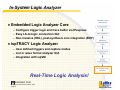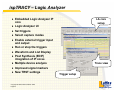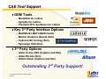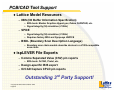
1
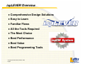
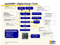
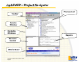
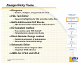
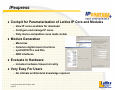
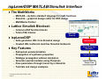
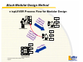
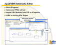
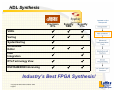
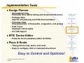
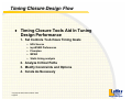
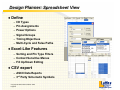
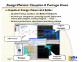
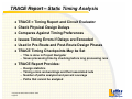
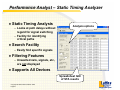
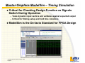
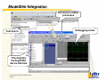
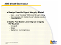
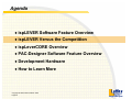
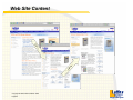
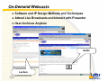
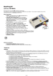
Lattice Semiconductor Corporation
Design Software
Intellectual Property
Development Hardware
Includes
ispLEVER (FPGA/CPLD Devices)
ispLeverCORE IP
PAC-Designer (Power Manager and ispCLOCK Devices)
Development Hardware / Evaluation Boards
Copyright © Lattice Semiconductor 2006
Page 1
Bringing the Best Together
ispLEVER Overview
♦ Comprehensive Design Solutions
♦ Easy to Learn
♦ Familiar Flows
“The Simple Machine for Complex Designs”
♦ All the Tools Required
♦ The Most Choice
♦ Best Performance
♦ Best Value
♦ Best Programming Tools
Copyright © Lattice Semiconductor 2006
Page 2
Bringing the Best Together
Agenda
♦ ispLEVER Software Feature Overview
♦ ispLEVER Versus the Competition
♦ ispLeverCORE Overview
♦ PAC-Designer Software Feature Overview
♦ Development Hardware
♦ How to Learn More
Copyright © Lattice Semiconductor 2006
Page 3
Bringing the Best Together
ispLEVER – Digital Design Tools
• IPexpress
IP cores and modules
• Text Editor
• Schematic Editor
• Waveform Editor
• Mentor Graphics ModelSim
• 3rd Party Simulators
• Mentor Graphics Precision RTL
• Synplicity Synplify
• TRACE
• Performance Analyst
Additional
Additional Design
Design support:
support:
-- Project
Project Manager
Manager
-- Revision
Revision Control
Control
-- HTML
HTML Reporting
Reporting
-- HTML
HTML Help
Help
-- CSV
CSV pin
pin export
export
-- IBIS
IBIS model
model export
export
Copyright © Lattice Semiconductor 2006
Page 4
IP
IP Cores
Cores //
Modules
Modules
MATLAB/
MATLAB/
Simulink
Simulink
• ispLeverDSP
60+ blockset functions
ModelSim integration
ispTRACY LA core integration
Design
Design Entry
Entry and
and
Simulation
Simulation
Power
Power Estimation
Estimation
Logic
Logic Synthesis
Synthesis
Design
Design Planning
Planning
Timing-Driven
Timing
Timing-Driven
Map,
Map, Place,
Place, and
and Route
Route
Preferences
Preferences
• Power Calculator
Power estimation
Free-form utilization or
design/VCD import
• Design Planner
Timing Constraints
Package/Pin
Floorplan View
Path Tracer
Static
Static Timing
Timing
Analysis
Analysis
• ispVM System
ISP
SPI
Embedded uP support
Device
Device Programming
Programming
On-Chip
On
On-Chip
Logic
Logic Analysis
Analysis
// Verification
Verification
• ispTRACY Logic Analyzer
Embedded LA core
LA GUI
Bringing the Best Together
ispLEVER Overview
♦ Two simple software configurations
– ispLEVER-Starter is a modular download from Lattice’s website
After 6 months software is non-operational
– ispLEVER includes all devices and 3rd party tools (Windows)
♦ $695 (US) List Price
– Contact your local Lattice Distributor or visit the Lattice online store
for offers
♦ ispLEVER includes Industry Leading 3rd Party Tools
– Competitors do NOT
– Synplify and Precision RTL synthesis
– ModelSim simulation
♦ ispLEVER includes MATLAB interface for DSP design
– Competitors do NOT
♦ ispLEVER includes logic analyzer for on-chip debug
♦ ispLEVER Available for Windows, Linux, and UNIX
Copyright © Lattice Semiconductor 2006
Page 5
Bringing the Best Together
ispLEVER – Design Tools Products
Part Number
SPLD,
GDX/2,
CPLD,
MachXO
Included
FPGA
Downloadable
All
LatticeECP2-50,
LatticeECP2-12,
All LatticeEC
All LatticeECP,
LatticeXP3, XP6
LS-HDL-BASE-PC-N
All
All
LS-EC6-BASE-PC-N
All
LS-XP10-BASE-PC-N
FPSC
Precision RTL Synplify ModelSim
Synthesis
Synthesis Simulation Eval Board
License
Type
Yes
Yes
All
Yes
Yes
Yes
All
All
Yes
Yes
Yes
EC6-std
Node Locked
All
All
All
Yes
Yes
Yes
XP10-std
Node Locked
LS-X2280-BASE-PC-N
All
All
All
Yes
Yes
Yes
XO2280-std Node Locked
ispLEVER for Unix
LS-ADV-WS-F
All
All
All
Floating
ispLEVER for Linux
LS-ADV-LX-F
All
All
All
Floating
Starter
Node Locked
Node Locked
ispLEVER for Windows
Floating License Upgrade
LS-FLOAT-PC
for Windows
Copyright © Lattice Semiconductor 2006
Page 6
Floating
Bringing the Best Together
ispLEVER: Easy and Quick to Learn
♦ Highlights
– FPGA Design Guide
»
»
»
»
Migrating Xilinx and Altera Designs
Synthesis Guidelines
Timing Closure Advice
On-Chip Debug Overview
– Numerous Design Tutorials
– HTML-Based Help Topics with Hyperlinks to Lattice Website
♦ Online Help
– Organized by Lattice Device Category (FPGA, CPLD, etc.) and
Design Tool (Power Calculator, Design Planner, etc.)
– FAST Search
Copyright © Lattice Semiconductor 2006
Page 7
Bringing the Best Together
Rich Educational Materials
–
–
–
–
Tutorials
FPGA Design Guide
Migration Advice
Hardware Feature How To Guides
It’s Easy to Get Started!
Copyright © Lattice Semiconductor 2006
Page 8
Bringing the Best Together
Help, Tutorials, and Design Advice
♦ HTML-based Help
♦ FPGA Design Guide
♦ Tutorials
Index &
Search
Web site x-refs
Web site links
Copyright © Lattice Semiconductor 2006
Page 9
Bringing the Best Together
Documentation
♦ “How To” Help Topics on
FPGA functions
–
–
–
–
–
–
–
Memories
sysIO Buffers
sysCLOCK PLL
sysCONFIG
sysDSP Blocks
DDR
More…
Copyright © Lattice Semiconductor 2006
Page 10
Bringing the Best Together
Software Overview
ispLEVER Project Management
Features and Tools
Design Entry
HDL Synthesis
Advanced Implementation Tools
Simulation and Analysis
Device Programming
In-system Logic Analysis
Copyright © Lattice Semiconductor 2006
Page 11
Bringing the Best Together
Project Management
♦ Project Navigator
– Source management and process control
♦ Revision Control
– Save and restore process state and related files
♦ HTML Reporting and Help
– Hyperlinked navigation and search of reports and help
♦ Tcl/Tk Tools
– Record and playback process sequences
Organize Design Files and Processes!
Copyright © Lattice Semiconductor 2006
Page 12
Bringing the Best Together
ispLEVER – Project Navigator
Process List
Toolbar
Source
Window
Dockable
Windows
Reports
Revision
Control
What’s New?
Copyright © Lattice Semiconductor 2006
Page 13
Bringing the Best Together
Project Navigator: Project Wizard
♦ Design setup <60s
♦ Wizard Choices:
–
–
–
–
Name the project
Select project type
Select device
Select source files
♦ When Finished…
User Is Designing
Copyright © Lattice Semiconductor 2006
Page 14
Bringing the Best Together
Design Entry Tools
♦ IPexpress
– Browse, configure, and generate IP cores
♦ HDL Text Editor
– Keyword highlighting for HDL and other native files
♦ MATLAB/Simulink DSP Blocks
– DSP-function blocks tailored for Lattice devices
♦ I/O Assistant method
– Flow enables early PCB handoff
– Comprehensive design rule checks
♦ Block Modular Design method
– Parallel development of sub-modules
– Non-invasive incremental design
♦ Schematic Editor
– Hierarchical block diagram editor
– Integrated FPGA libraries
♦ ABEL for CPLD and SPLD
Copyright © Lattice Semiconductor 2006
Page 15
Bringing the Best Together
IPexpress
♦ Cockpit for Parameterization of Lattice IP Core and Modules
– View IP cores available for download
– Configure and manage IP cores
– Only device-compatible cores made visible
♦ Module Generation
–
–
–
–
Memories
Common digital macro functions
sysCLOCK PLL and DLL
DDR interfaces
♦ Evaluate in Hardware
– Includes hardware timeout circuitry
♦ Very Easy For Users
– No intimate architectural knowledge required
Copyright © Lattice Semiconductor 2006
Page 16
Bringing the Best Together
ispLeverDSP MATLAB/Simulink Interface
♦ The MathWorks
– MATLAB – de-facto standard language for math functions
– Simulink – graphical design editor for DSP design
– MathWorks Partner
Simulink Graphical Editor
♦ Lattice Simulink Blockset:
– Common DSP function blocks
– Total of 60+ blocks
♦ ispLeverDSP
MATLAB/
MATLAB/
Simulink
Simulink
– Auto-generates HDL from Simulink design
– Created HDL testbench matches Simulink testbench
♦ Key Features
–
–
–
–
–
–
Subsystem parameterization
Propagation of synthesis properties
Datatype propagation without simulation
Generate special modules using IPexpress
Pass parameters through hierarchy in Simulink
Tutorials and design examples
Copyright © Lattice Semiconductor 2006
Page 17
ispLeverDSP
Design
Entry
and
Design
Entryand
and
HDL
Capture
Simulation
Simulation
Simulation
Logic
Logic Synthesis
Synthesis
LatticeECP2/ECP
Design Flow
Bringing the Best Together
I/O Assistant Method
♦ ispLEVER Process Flow for I/O Planning
♦ Supports Early PCB Handoff
– Select / Check / Lock Pins Before Design is Complete
– Output to CSV Formatted File
– Comprehensive Design Rule Checks for I/O Compatibility
before Map, Place, and Route
♦ I/O Module Generation for Complex Interfaces
– LatticeECP2/ECP/EC/XP
» DDR_GENERIC
» DDR_MEM
– LatticeSC
» DDR
» SDR
» DQS
Copyright © Lattice Semiconductor 2006
Page 18
Bringing the Best Together
Block Modular Design Method
♦ ispLEVER Process Flow for Modular Design
T
A
B
Re
bu sou
an dge rce
d t ti n
im g
ing
Ne
re w bu
inc ques dge
ve rem ts o t
ri f
r
ica enta
t io l
n
MPAR
D
MPAR
A
Verify
Team member A
System Engineer
A
Design
Verify
Design
MPAR
B
Verify
Team member B
bly
m
e
s
As
B
Program
C
System Engineer
Copyright © Lattice Semiconductor 2006
Page 19
Bringing the Best Together
ispLEVER Schematic Editor
♦ Block Diagrams
♦ Gate-Level FPGA Library
♦ Import HDL Modules from RTL or IPexpress
♦ VHDL or Verilog HDL Export
Schematic-related
processes
HDL
Copyright © Lattice Semiconductor 2006
Page 20
Bringing the Best Together
HDL Synthesis
Precision
RTL
Synplify
OEM
Synplify
Pro
9
9
9
9
SystemVerilog
9
9
9
Constraints
Editor
9
9
9
PAR
Integration
9
9
RTL/Technology View
9
9
DSP/RAM/ROM Inferencing
9
VHDL
Verilog
9
9
Industry’s Best FPGA Synthesis!
Copyright © Lattice Semiconductor 2006
Page 21
Bringing the Best Together
Precision RTL Synthesis for Lattice
RTL view
P&R
Integration
Critical path /
Technology view
Copyright © Lattice Semiconductor 2006
Page 22
Bringing the Best Together
Precision RTL Synthesis
♦ Mentor’s Latest Synthesis Tool
– Much better fMAX and area utilization than LeoSpec
– Performance very close to Synplicity’s Synplify
– More user friendly than LeoSpec
♦ No Differences vs. Mentor’s Full Up System
♦ Fully Integrated in ispLEVER
♦ Includes:
–
–
–
–
Schematic viewer
RAM inferencing
ROM inferencing
Register retiming
Copyright © Lattice Semiconductor 2006
Page 23
Bringing the Best Together
Synplify for Lattice
♦ Synplicity’s RTL Synthesis Tool
♦ OEM Version for Lattice Included With ispLEVER
♦ Synplify Pro support now
Copyright © Lattice Semiconductor 2006
Page 24
Bringing the Best Together
Implementation Tools
♦ Design Planner
– Spreadsheet View
Excel-like UI to define timing and location Preferences
– Package View
Ideal for I/O planning and PCB documentation
– Floorplan View
View placement, critical paths, congestion, and groups
– Path Tracer
Highlight critical paths
– Pin CSV Export
♦ EPIC Device Editor
– Powerful device database editor for ECOs
♦ Place & Route
– Timing-driven map, place, and route
– Easy to configure, GUI or command-line driven
Easy to Control and Optimize!
Copyright © Lattice Semiconductor 2006
Page 25
Bringing the Best Together
Timing Closure Design Flow
♦ Timing Closure Tools Aid In Tuning
Design Performance
1. Set Controls To Achieve Timing Goals
»
»
»
»
»
HDL Source
ispLEVER Preferences
Floorplan
MPAR
Static timing analysis
2. Analyze Critical Paths
3. Modify Constraints and Options
4. Iterate As Necessary
Copyright © Lattice Semiconductor 2006
Page 26
Bringing the Best Together
ispLEVER Preference Language
♦ The Nexus Between Design and Performance
♦ Flexible ASCII Language for Timing-Driven MPAR and STA
♦ Graphical Spreadsheet-Like UI Entry Easy
– Assign Globals, Period/Frequency, I/O Timing, Timing Exceptions
FREQUENCY NET "pll_nclk" 133.000000 MHz ;
FREQUENCY NET "pll_mclk" 133.000000 MHz ;
FREQUENCY NET "clk_c" 133.000000 MHz ;
FREQUENCY PORT "clk" 133.000000 MHz ;
DEFINE PORT GROUP "group_dq" "ddr_dq_0"
"ddr_dq_1"
"ddr_dq_2"
"ddr_dq_3"
"ddr_dq_4"
"ddr_dq_5"
"ddr_dq_6"
"ddr_dq_7" ;
CLOCK_TO_OUT GROUP "group_dq" 10.000000 ns CLKPORT "clk" ;
PROHIBIT SITE "EBR_R19C10" ;
PROHIBIT SITE "EBR_R19C8" ;
PROHIBIT SITE "EBR_R19C6"
Copyright © Lattice Semiconductor 2006
Page 27
Bringing the Best Together
Design Planner: Spreadsheet View
♦ Define
–
–
–
–
–
–
I/O Types
Pin Assignments
Power Options
Signal Groups
Timing Objectives
Multi-Cycle and False Paths
♦ Excel-Like Features
– Sorting and Pin Type Filters
– Context Sensitive Menus
– Fill Up/Down Editing
♦ CSV export
– ASCII Data Reports
– 3rd Party Schematic Symbols
Copyright © Lattice Semiconductor 2006
Page 28
Bringing the Best Together
Design Planner: Floorplan & Package Views
♦ Graphical Design Viewer and Editor
– Used for Timing, Location, and Buffer Constraints
– Used for pin assignment, grouping signals, placement,
critical path analysis, routing analysis, … more
– Useful in performance optimization and timing closure
Logical
Floorplan
Path Tracer
Package
Copyright © Lattice Semiconductor 2006
Page 29
Physical
Floorplan
Bringing the Best Together
Place & Route Setup
Placement effort
Routing passes
Copyright © Lattice Semiconductor 2006
Page 30
Bringing the Best Together
Register Retiming
♦ Balances Combinational Logic
Across Register-Pairs
– Maximizes fMAX according to the
constraints: tSU, tCO or fMAX in
preference file (.prf).
♦ Typically Improves fMAX by 5-10%
♦ Controllable Option for Users
♦ “NOMERGE” Attribute in
Verilog/VHDL
– Added to each IO register where
retiming is not desired
Copyright © Lattice Semiconductor 2006
Page 31
Bringing the Best Together
Nodal Control for CPLD
♦ Constraints Added to Critical Nodes to Increase fMAX
–
–
–
–
Decreases Levels of Logic Æ Improves Fmax
Limits PTERM usage
Limits Fanin
Takes advantage of XOR function
Copyright © Lattice Semiconductor 2006
Page 32
Bringing the Best Together
EPIC – Device Editor
Tools for Device and Board Level Design Analysis
♦ Make Changes to NCD
♦ Place and route critical
components before PAR
♦ Place and route critical
signals after PAR
♦ Manually complete
unrouted signals
♦ Perform Physical DRC
♦ Examine TRACE results
♦ Route buried signals to
unused pins
Copyright © Lattice Semiconductor 2006
Page 33
Bringing the Best Together
Simulation and Analysis
♦ ModelSim for Lattice
–
–
–
–
VHDL/Verilog/SystemVerilog language simulation
Tight script-based integration
Pre-compiled Lattice device library resources
Mentor Graphics Questa support available now
♦ TRACE
– Timing Report and Circuit Evaluator
– Constraints-driven Static Timing Analysis (STA)
– Supports multi-cycle relationships and timing exceptions
♦ Performance Analyst
– Easy to use tabular view for static timing analysis
♦ Power Calculator
– Estimate AC and DC power consumption
– Simulation data (VCD) import
– Configure power supply requirements
Verify Function, Timing, and Power!
Copyright © Lattice Semiconductor 2006
Page 34
Bringing the Best Together
ispLEVER Design Flow – Verification
Tools for Device and Board Level Design Analysis
♦ Static Timing Analysis (STA)
–
–
–
–
Preference-driven STA
fMAX, tCO, tH
Multi-cycle
Timing exceptions
♦ Timing Simulation
– Functional verification based on switching vectors to check for
timing violations
♦ Logic Analyzer
– Embedded logic analyzer with external probe points and triggers to
capture internal (otherwise unobservable) signals
♦ Power Estimation
– Accurately models device power consumption so that board power
budgets may be checked
♦ IBIS Modeling
– Signal integrity models to perform board level evaluation of noise
and crosstalk generated on board level traces
Copyright © Lattice Semiconductor 2006
Page 35
Bringing the Best Together
TRACE Report – Static Timing Analysis
♦ TRACE = Timing Report and Circuit Evaluator
♦ Check Physical Design Delays
♦ Compares Against Timing Preferences
♦ Issues Timing Errors if Delays are Exceeded
♦ Used in Pre-Route and Post-Route Design Phases
♦ TRACE Timing Checkpoints May be Set
– This is done in Project Navigator
– Saves processing time by checking before long processing runs
♦ TRACE Report Provides:
–
–
–
–
Design statistics
Timing errors and warnings and their associated nets
Number of paths analyzed and percent coverage
Paths that cannot be analyzed
Copyright © Lattice Semiconductor 2006
Page 36
Bringing the Best Together
Performance Analyst – Static Timing Analyzer
♦ Static Timing Analysis
Analysis options
– Looks at path delays without
regard for signal switching
– Facility for identifying
critical paths
♦ Search Facility
– Easily find specific signals
♦ Filtering Features
– Unwanted nets, signals, etc.,
are not displayed
♦ Supports All Devices
Spreadsheet GUI
of STA results
Copyright © Lattice Semiconductor 2006
Page 37
Bringing the Best Together
Mentor Graphics ModelSim – Timing Simulation
♦ Critical for Checking Design Function as Signals
Switch During Operation
– Tests dynamic input vectors and validates against expected output
– Critical for finding setup and hold time violations
♦ ModelSim is the De-facto Standard for FPGA Design
Copyright © Lattice Semiconductor 2006
Page 38
Bringing the Best Together
Power Calculator for FPGA
♦ Allows User to Determine
Power Supply Requirements
♦ Toggle Rate Estimate Input
♦ VCD Import
♦ Total Power Summary Table
♦ Power and Icc Views
♦ XML Summary
♦ Parameters:
–
–
–
–
–
Airflow
Heatsink
Ambient temperature
Operating condition
Frequency
Copyright © Lattice Semiconductor 2006
Page 39
Bringing the Best Together
ModelSim LATTICE
♦ RTL and Gate-Level Simulation
– VHDL and Verilog Language Support
» However, mixed languages NOT supported
» Customer must buy mixed language support
♦ De-facto Standard for FPGA Design
♦ NO RTL Line Limit in the Lattice OEM Version
– Very good performance
♦ Included With ispLEVER (Windows) Package
♦ ispLEVER Automates “Do” File Creation
– Makes the simulation easier to set up and use
Copyright © Lattice Semiconductor 2006
Page 40
Bringing the Best Together
ModelSim Integration
Simulation-related
processes
Test bench
.do
Debugging views
Precompiled
Verilog/VHDL
device libraries
Copyright © Lattice Semiconductor 2006
Page 41
Bringing the Best Together
Device Programming
♦ Supports All Lattice Devices
–
–
–
–
IEEE 1149.1 in-system programming
SPI Flash programming support
TransFR support
Multiple programming format support
» ISC BSDL/Data, SVF, JEDEC, IEEE 1532, etc.
– Format translation, Universal File Writer (UFW)
♦ ispVM Embedded
– Device programming via embedded processors
– VME source code provided
♦ Serial Vector Format (SVF) Debugger
♦ ATE Programming Vector Generator
♦ USB Gang Programming (DLxConnect)
Industry’s Best Programming Solution!
Copyright © Lattice Semiconductor 2006
Page 42
Bringing the Best Together
In-System Logic Analyzer
♦ Embedded Logic Analyzer Core
– Configure trigger logic and trace buffer via IPexpress
– Easy LA-to-logic connection GUI
– Non-invasive (HDL), post-synthesis core integration (EDIF)
♦ ispTRACY Logic Analyzer
– User defined triggers and capture modes
– List or wave format analyzer GUI
– Integration with ispVM
Real-Time Logic Analysis!
ROADMAP ITEM
Copyright © Lattice Semiconductor 2006
Page 43
Bringing the Best Together
ispTRACY – Logic Analyzer
♦ Embedded Logic Analyzer IP
core
LA core
setup
♦ Logic Analyzer UI
♦ Set triggers
♦ Select capture modes
♦ Enable external trigger input
and output
♦ Run or stop the triggers
♦ Waveform and List Display
♦ Post Synthesis (EDIF)
integration of IP cores
♦ Multiple device analysis
Trace view
♦ Improved signal markers
♦ New TRST settings
Copyright © Lattice Semiconductor 2006
Page 44
Trigger setup
Bringing the Best Together
CAE Tool Support
♦ OEM Tools
– ModelSim for Lattice
– Synplify for Lattice
– Precision RTL Synthesis for Lattice
♦ Key 3rd Party Interface Options
–
–
–
–
MathWorks MATLAB/Simulink
Mentor Graphics Questa (Sim)
Cadence NC-Verilog (Sim)
Synopsys VCS (Sim)
♦ 3rd Party Options
– Aldec Active-HDL (Capture and Sim)
– Aldec Riviera (Sim)
– Altium Nexar (Capture and Sim)
Outstanding 3rd Party Support!
Copyright © Lattice Semiconductor 2006
Page 45
Bringing the Best Together
PCB/CAD Tool Support
♦ Lattice Model Resources
– IBIS (I/O Buffer Information Specification)
» EDA tools: Mentor Graphics HyperLynx, Zuken CADSTAR, etc.
» Signal integrity (SI) simulation (<1GHz)
– SPICE
» Signal integrity (SI) simulation (>1GHz)
» Requires factory NDA and Synposys HSPICE
– BSDL (Boundary Scan Description Language)
» Boundary scan chain models describe devices in a JTAG-compatible
scan chain
♦ ispLEVER File Exports
– Comma Separated Value (CSV) pin reports
» EDA tools: OrCAD, Protel, etc.
– Design-specific IBIS export
– OrCAD Capture CPLD pin reports
Outstanding 3rd Party Support!
Copyright © Lattice Semiconductor 2006
Page 46
Bringing the Best Together
IBIS Model Generation
♦ Design Specific Signal Integrity Model
– Uses a base “template” IBIS model for each family
– Generates specific model of user’s design based on
resources used
♦ Useful For Board Level Signal Integrity
Verification
– Crosstalk
– Noise
– Signal loss over long traces
Copyright © Lattice Semiconductor 2006
Page 47
Bringing the Best Together
ispLEVER 6.0 (Plus SP1) - What’s New?
♦ LatticeECP2-50
+ ECP2-12 in SP1
(Preliminary Timing)
♦ LatticeSC15, 25, and 80
(Contact Lattice)
♦ IPexpress Web Interface
♦ Design Planner
– Easier and faster I/O planning
– Advanced floorplanning and
preference editing
♦ Schematic Library For FPGA
♦ DSP Design Enhancements
– Device support for: ECP2,
SC/SCM, EC, XP, and XO
– MATLAB/Simulink reference
designs
– Floating to Fixed point
conversion tutorial
♦ Aldec, Cadence, and
Synopsys simulators
qualified
Copyright © Lattice Semiconductor 2006
Page 48
♦ Expanded Precision RTL and
Synplify Controls
– TCL Format project files
– Easier report access
– Expanded tool controls
♦ CPLD Pin Export for OrCAD
Capture
♦ Project Navigator: Top-Level
HDL/Schematic Module
Selector
♦ Text Editor: HDL Template
Preview
♦ Power Calculator: Command
line interface
– Updated in SP1 to improve
accuracy
♦ Precision RTL Synthesis
2005C Update 2
♦ ModelSim LATTICE 6.1D
♦ Synplify for Lattice 8.6A
Bringing the Best Together
Agenda
♦ ispLEVER Software Feature Overview
♦ ispLEVER Versus the Competition
♦ ispLeverCORE Overview
♦ PAC-Designer Software Feature Overview
♦ Development Hardware
♦ How to Learn More
Copyright © Lattice Semiconductor 2006
Page 49
Bringing the Best Together
Software Orientation
Project Navigator
Modular Design
HDL Editor
ECS
CORE Generator
Constraints Editor
Floorplanner
Project Navigator
LogicLock
Text Editor
Block Editor
MegaWizard Plug-In Mgr
Assignment Editor
Floorplan Editor
ModelSim or 3RD
Functional
party simulation tools
Simulation
Waveform Editor
ModelSim or 3RD party
simulation tools
Simulator or 3RD party
simulation tools
Waveform Editor
Power
Power Calculator
Estimation
XPower
PowerPlay
Design
Entry
Project Navigator
Block Modular Design
Text Editor
Schematic Editor
IPexpress
Design Planner
Design Planner
ispLEVER
Copyright © Lattice Semiconductor 2006
Page 50
ISE
Quartus II
Bringing the Best Together
Software Orientation
Precision RTL or
Synplify
Design
Implementation NGDBUILD
MAP
PAR
XST or 3rd party
NGDBUILD
MAP
PAR
QII Integrated
Synthesis or 3rd party
Fitter
Timing
Analysis
TRACE and
Performance Analyst
TRACE and
Timing Analyzer
Timing Improve. Wiz.
Programming
Configuration
BITGEN
ispVM
BITGEN
iMPACT
Assembler
Programmer
On-Chip
Debugging
ispTRACY
ChipScope
SignalTap II
ispLEVER
Copyright © Lattice Semiconductor 2006
Page 51
ISE
Quartus II
Bringing the Best Together
Migrating a Xilinx ISE User to ispLEVER
♦ Includes industry standard synthesis tools
♦ Includes ModelSim
♦ Many similarities: MAP, PAR, TRACE, and EPIC
Module/IP Manager
*.v/.vhd
module.v/.vhd
Build Database
Synthesis and
Translation
project.ngd
project.prf
Map Design
Place & Route Design
project.ncd
Map TRACE Report /
Place & Route TRACE Report
Copyright © Lattice Semiconductor 2006
Page 52
project.tw1
project.twr
Logical to
Physical Mapping
Static Timing
Analysis
Bringing the Best Together
Migrating FPGA Designs
♦ FPGA Design Guide
– Chapter 2: FPGA Design for Altera Users
– Chapter 3: FPGA Design for Xilinx Users
♦ Replace Library
♦ Replace Specific Primitives in Source with
Equivalent Primitives
♦ Replace Modules
♦ Replace Constraints with Preferences
♦ Optimize HDL-Inferred Modules
Copyright © Lattice Semiconductor 2006
Page 53
Bringing the Best Together
LatticeECP/2 – Performance Advantage!
Fmax Index
LUT Index
100
97
100
80
100
76
100
99
98
91
80
70
60
60
40
40
20
20
0
0
EC-5
(130nm)
ECP2-7
(90nm)
Spartan3-5
(90nm)
Cyclone2-6
(90nm)
EC-5
(130nm)
ECP2-7
(90nm)
Spartan3-5
(90nm)
Cyclone2-6
(90nm)
• Average of benchmark designs using high effort
• Tools used: ispLEVER 6.0.00.24, Synplify 8.5d(OEM); Xilinx ISE 8.1SP1, SynplifyPro 8.2;
Altera Quartus 5.0SP1, SynplifyPro 8.2
• Command line: Map, Place, Route, and Timing Report
• Machine used: Pentium4 2.8 GHz, 2 GB, Windows 2000
• ECP2–7; EC-5; Spartan3-5; Cyclone2–6
Copyright © Lattice Semiconductor 2006
Page 54
Bringing the Best Together
LatticeSC Family – Performance Advantage!
Fmax Index
100
LUT Index
100
93
91
100
80
60
60
40
40
20
20
0
0
Virtex4-12
(90nm)
Stratix2-4
(90nm)
98
91
80
SC-7
(90nm)
100
SC-7
(90nm)
Virtex4-12
(90nm)
Stratix2-4
(90nm)
• Average of benchmark designs using high effort
• Tools used: ispLEVER 6.0.00.24, Synplify 8.5d(OEM); Xilinx ISE 8.1SP1, SynplifyPro 8.2;
Altera Quartus 5.0SP1, SynplifyPro 8.2
• Command line: Map, Place, Route, and Timing Report
• Machine used: Pentium4 2.8 GHz, 2 GB, Windows 2000
• ECP2–7; EC-5; Spartan3-5; Cyclone2–6
Copyright © Lattice Semiconductor 2006
Page 55
Bringing the Best Together
Conclusion
♦ Complete Solutions for All Your Needs
♦ Industry Leading Synthesis and Simulation Tools
– From Mentor Graphics and Synplify
♦ Easy to Use and Easy to Learn
♦ Familiar Flow and File Extensions
♦ Unsurpassed Performance and Productivity
♦ Industry’s Best Value
“The Simple Machine for Complex Designs”
Copyright © Lattice Semiconductor 2006
Page 56
Bringing the Best Together
Agenda
♦ ispLEVER Software Feature Overview
♦ ispLEVER Versus the Competition
♦ ispLeverCORE Overview
♦ PAC-Designer Software Feature Overview
♦ Development Hardware
♦ How to Learn More
Copyright © Lattice Semiconductor 2006
Page 57
Bringing the Best Together
IP Core Portfolio
♦ Downloadable Reference Designs
– www.latticesemi.com
♦ ispLeverCORE IP
– Lattice Semiconductor Corp
♦ ispLeverCORE Connection Partners
–
–
–
–
–
CAST
Digital Core Design (DCD)
Elliptic
Eureka Technologies
Northwest Logic
Copyright © Lattice Semiconductor 2006
Page 58
Bringing the Best Together
ispLeverCORE IP
♦ Available for Purchase from Lattice
– Evaluation version available for download from the Lattice website
– Netlist or Source available
– Board or Site licenses
♦ Includes:
–
–
–
–
–
–
Description
Features summary
Configurations available
User’s Guide
Evaluation capability
Tech Note / Brochure (selected functions)
43 Unique Functions
♦ Where to Find the List of IP Available
– Search screen:
http://www.latticesemi.com/products/intellectualproperty/
Copyright © Lattice Semiconductor 2006
Page 59
Bringing the Best Together
Reference Designs
♦ Available for Download from Lattice Website
– Free of charge
♦ Includes:
–
–
–
–
–
–
–
Description
Features summary
Configurations Available
User’s Guide
Source Code
Tech Note / Brochure (selected functions)
Demonstration design (selected functions)
28 Unique Functions
♦ Where to Find the List of Reference Designs
– Search screen:
http://www.latticesemi.com/products/intellectualproperty/
Copyright © Lattice Semiconductor 2006
Page 60
Bringing the Best Together
ispLeverCORE Connections Partners
♦ 3rd Party Developed, Sold, and Supported
♦ Augments The Lattice Portfolio
– Adds functions for applications for which we have little
experience or expertise
♦ Leverage 3rd Party Expertise
– Experts create and support complex functions
♦ Faster Time to Market
– 3rd Parties act as resources to port and support
Copyright © Lattice Semiconductor 2006
Page 61
Bringing the Best Together
LatticeMico8 – 8-Bit Microcontroller
♦ Optimized For Lattice Leading-Edge Families
– LatticeECP/EC, LatticeXP, and MachXO
♦ Targeted Towards Wide Variety Of Applications
– Consumer, Computation, Communications, Medical, Industrial, Auto
♦ Innovative Open IP Core License
♦ Key Architectural Features
–
–
–
–
–
–
–
–
Gold Medal
2005
Readers Award
Embedded
Control
Europe
8-Bit Data Path
18-Bit Wide Instructions
Two Cycles Per Instruction
32 General Purpose Registers
32 Bytes Of Internal Scratch Pad Memory
Input/Output Is Performed Using Ports (Up To 256 Port Numbers)
Optional 256 Bytes Of External Scratch Pad RAM
Lattice UART Reference Design Peripheral
♦ Source, Documentation, Everything Needed for Design
Copyright © Lattice Semiconductor 2006
Page 62
Bringing the Best Together
Agenda
♦ ispLEVER Software Feature Overview
♦ ispLEVER Versus the Competition
♦ ispLeverCORE Overview
♦ PAC-Designer Software Feature Overview
♦ Development Hardware
♦ How to Learn More
Copyright © Lattice Semiconductor 2006
Page 63
Bringing the Best Together
PAC-Designer – Mixed Signal Design Tool
♦ Complete Mixed Signal Design Tool
♦ Self Contained Support for All ispPAC Devices:
♦ Fully Integrated Design and Simulation Environment
♦ High Level Logic Design Mechanism
LogiBuilder for CompactPCI
Frequency Synthesizer
PAC-Designer GUI for ispPAC Power Manager
Copyright © Lattice Semiconductor 2006
Page 64
Bringing the Best Together
PAC-Designer – Design Tool Features
♦ Easy-to-use GUI
♦ SPICE model export
♦ Design Entry
– LogiBuilder, Hierarchical design entry, High level design entry power
management, Standard circuit generation library
♦ Design Utilities
– Clock frequency synthesis, Graphical skew editing, Frequency calculators
♦ Simulation
– Create stimulus graphically, Digital Waveform simulation, View both gain
and phase plots graphically, Simultaneously view inputs and outputs,
Cross-hair cursors to directly read any gain or phase magnitude
♦ Facilitates Manufacturing Automation
– Library of automation functions, Circuit board for different, Example
program and documentation
Copyright © Lattice Semiconductor 2006
Page 65
Bringing the Best Together
Complete Power Management Design in 5 Steps
1. Set Power Supply
Threshold For Each
Analog Input
5. In-System
Program the Design
Through JTAG
Copyright © Lattice Semiconductor 2006
Page 66
Lattice PAC-Designer Software
2. Set Power Supply
Ramp Rate for Each
FET Driver
3. Complete Sequencing
and Monitoring Design
Using LogiBuilder
4. Verify Using
Waveform Simulator
Bringing the Best Together
Complete Clock Net Design in 5 Steps
Lattice PAC-Designer Software
1. Specify I/O
Interface Type and
Divider
5. Print Summary
Report
4. Download Design
Configuration to
CLK5520 for
Verification
2. Synthesize M,N,V
Counter From
Output Frequencies
3. Graphically
Adjust Skew For
Each Clock Output
Copyright © Lattice Semiconductor 2006
Page 67
Bringing the Best Together
Agenda
♦ ispLEVER Software Feature Overview
♦ ispLEVER Versus the Competition
♦ ispLeverCORE Overview
♦ PAC-Designer Software Feature Overview
♦ Development Hardware
♦ How to Learn More
Copyright © Lattice Semiconductor 2006
Page 68
Bringing the Best Together
Evaluation Boards
♦ Wide Range of Evaluation Boards
–
–
–
–
–
LatticeSC / ECP2 / ECP-DSP / EC / XP / XPGA FPGAs
Lattice MachXO Crossover PLD
Lattice ORCA FPSCs
ispMACH 4000 / ispXPLD CPLDs
ispCLOCK Evaluation Board
ispPAC / ispCLOCK
LatticeEC Standard Evaluation Board
LatticeEC Advanced Evaluation Board
Copyright © Lattice Semiconductor 2006
Page 69
Bringing the Best Together
LatticeECP2 Standard Evaluation Board
♦ Features:
–
–
–
–
–
–
64-bit PCI/PCI-x edge connector and form factor
RS-232 & RJ-45 Connectors
Compact Flash Connector
On-board Flash configuration memory
Prototype area
Various LEDs, switches, connectors, headers, and on-board power
supply
– Includes: ispDOWNLOAD Cable for device programming
– Includes: AC power supply (International wall plug-in)
♦ 484 fpBGA Device
– ECP2-50: LFE2-50E-6F484C
♦ Availability
– Available Now
♦ On the web
– User guide (including schematics), sample program.
Copyright © Lattice Semiconductor 2006
Page 70
Bringing the Best Together
LatticeECP2 Standard Evaluation Board
Compact Flash
Connector
8-bit
switch and
LEDs
7-segment
LED
SMA
connectors
(optional)
On-board
power
supply
Prototype
area
RS-232
RJ-45
64-bit PCI
edge
Copyright © Lattice Semiconductor 2006
Page 71
LatticeECP2
FPGA
33.33 MHz
Oscillator
Bringing the Best Together
LatticeECP2 Advanced Evaluation Board
♦ Features:
–
–
–
–
–
–
–
–
–
Dual DDR2 SO DIMM memory sockets
10/100/1G Ethernet PHY with RJ-45 interface
SPI4.2 TX/Rx Connectors
RS232 Driver/Receiver
USB Transceiver
LCD panel interface
TI EMIF Interface Connector
On-board SPI-Flash configuration memory
Various LEDs, switches, connectors, headers, SMAs, on-board
power supply, Lattice PAC-POWR1220AT8 Power Manager
♦ 672 ball device
– LFE2-50E-6F672C
♦ Availability
– Available Now
♦ On the web
– User guide (including schematics), sample program.
Copyright © Lattice Semiconductor 2006
Page 72
Bringing the Best Together
LatticeECP2 Advanced Evaluation Board
E-net PHY
On-board
power
supply
RJ-45
Compact Flash
Connector
33.33 MHz
Oscillator
SPI4 connectors
8-bit
switch and
LEDs
DDR SODIMMs
LatticeECP2
FPGA
RS-232
Copyright © Lattice Semiconductor 2006
Page 73
USB
Prototype
area
7-segment
LED
Bringing the Best Together
LatticeSC Communications Board
♦ Features:
–
–
–
–
–
–
–
–
–
–
300-pin MSA transponder for SFI-4.1/XSBI applications
Molex VHDM interconnection for SPI4.2
200-pin DDR SODIMM socket
SMA test points for high-speed SERDES (4 channels, 4 SMA each)
and Clock I/O
On-board power control
On-board oscillator
On-board clock management
Various high-speed layout structures
On-board flash configuration memory
Various LEDs, switches, connectors, headers, etc.
♦ 900 ball device
– LatticeSC: LFSC3GA25E-6F900C
♦ Availability
– Contact your Lattice Representative
♦ On the web
– User Guide and general info
Copyright © Lattice Semiconductor 2006
Page 74
Bringing the Best Together
LatticeSC Communications Board
SMA for
SERDES I/O
300-pin MSA
LatticeSC
FPGA
SMA for clock I/O
DDR DIMM
ispCLOCK
and Power
Manager
Oscillator
On-board
power
control
Copyright © Lattice Semiconductor 2006
Page 75
Bringing the Best Together
LatticeSC Standard Board
♦ Features:
– X8 PCIexpress edge connector / form factor
– On-board DDR2 Memory
– SMA Connectors for SERDES I/O, LVDS evaluation, and external
clock I/O
– BNC edge connectors for Digital Video Interface
– On-board Flash configuration memory
– Various LEDs, switches, connectors, headers, and on-board power
control
♦ 1152 ball device
– LatticeSC: LFSC3GA80E-6FF1152C
♦ Availability
– 3Q 2006
♦ On the web
– Related info coming soon!
Copyright © Lattice Semiconductor 2006
Page 76
Bringing the Best Together
LatticeEC Standard Evaluation Board
♦ Features:
–
–
–
–
–
PCI connector
oscillator socket / ext clock
1.2V & 3.3V on-board power (banana jacks also available)
SPI flash on-board
Pads for high-speed SMA connectors (not populated)
♦ 484-ball device
– EC6: LFEC6E-L-EV – List Price = $149
– EC20: LFEC20E-L-EV – List Price = $175
– ECP20: LFECP20E-L-EV – List Price = $175
♦ Availability:
– Available Now
♦ On the web
– PCI evaluation bitstream available
– Note there are both Rev A and Rev B PCBs = each has unique user
manual/schematics
Copyright © Lattice Semiconductor 2006
Page 77
Bringing the Best Together
LatticeEC Standard Evaluation Board
Prototype area
Power Circuitry
SMA Pads
Clocks, PLL
On-board
oscillator
LatticeEC
LFEC20E-5F484C
Copyright © Lattice Semiconductor 2006
Page 78
PCI interface
SPI Flash
Bringing the Best Together
LatticeEC Advanced Evaluation Board
♦ Features:
–
–
–
–
–
–
–
–
–
FCRAM on-board
DDR socket
SPI4.2 interface
RJ-45 interface
PCI slot
Multiple voltage planes
SPI Flash on-board
SMA connectors for high-speed signals / clocks
On-board/ext clock, etc.
♦ 672-ball device
– EC20: LFEC20E-H-EV – List Price = $1295
– ECP20: LFECP20E-H-EV – List Price = $1295
♦ Availability
– Contact your Lattice Representative
♦ On the web
–
–
–
–
PCI evaluation bitstream available
FCRAM evaluation bitstream available
DDR evaluation bitstream available
User manual w/ schematics
Copyright © Lattice Semiconductor 2006
Page 79
Bringing the Best Together
LatticeEC Advanced Evaluation Board
DDR Memory slot
LatticeEC
LFEC20E-5F672C
FCRAM
SPI Flash
Prototype
area
Power Circuitry
On-board
oscillator
Ext. Clock-in
RJ-45
connector
(CAT-5
cable)
SPI 4.2
PLL
Copyright © Lattice Semiconductor 2006
Page 80
PCI interface
Voltage plane
selection
Bringing the Best Together
LatticeXP Standard Evaluation Board
♦ Features:
–
–
–
–
–
–
Multiple power planes (external sources available)
On board oscillator
SMA pads for high-speed signaling (SMA pads not populated)
LEDs & switches for feedback & configuration
Generous prototype area
On-board power supply (Note: Initial Rev. A boards did not include
this)
♦ 256-ball device
– XP10: LFXP10C-L-EV
♦ Availability
– Rev B boards now including AC adapter and download cable.
♦ On the web
– User manual, sample program.
Copyright © Lattice Semiconductor 2006
Page 81
Bringing the Best Together
LatticeXP Standard Evaluation Board
Prototype
area
LatticeXP
LFXP10C-5F256C
Programming
Interface
LEDs
Power Circuitry
SMA pads
On-board
oscillator
Prototype area
Copyright © Lattice Semiconductor 2006
Page 82
Bringing the Best Together
LatticeXP Advanced Evaluation Board
♦ Features:
–
–
–
–
–
–
–
LFXP10C-5F388C FPGA Device
DDR memory interface socket
10/100/1G E-net MAC interface
PCI interface
On-board FCRAM
On-board oscillator
Various LEDs, SMA connections for external clocking, and on-board
power control
♦ 388-ball device
– XP10: LFXP10C-H-EV – List Price = $1295
♦ Availability
– Contact your Lattice Representative
♦ On the web
– Evaluation bitstreams when available
– User manual w/ schematics when available
Copyright © Lattice Semiconductor 2006
Page 83
Bringing the Best Together
LatticeXP Advanced Evaluation Board
LatticeXP
LFXP10C-5F388C
DDR Memory slot
Power Circuitry
FCRAM
On-board
oscillator
Ext. Clock-in
E-net connector
E-net
PHY
Copyright © Lattice Semiconductor 2006
Page 84
PCI interface
Voltage plane
selection
Bringing the Best Together
MachXO Starter Evaluation Board
♦ Features
–
–
–
–
–
–
–
–
–
–
MachXO device
Power input jack
33MHz oscillator
Status LEDs, and 9 I/O LEDs
8-bit input switch
Access to all device I/O
Prototyping area
Landing pads for off-board expansion connectors
AC adapter Included (International plugs!)
Download Cable Included: HW-DL-3C
♦ 100-TQFP device
– MachXO-256: LCMXO256C-4T100C
♦ Availability
– Shipping today, order via on-line store, or through your Distributor
– Board + AC Adapter + Download Cable = $99, An incredible value!
♦ On the web
– User Manual available for download, includes schematics.
Copyright © Lattice Semiconductor 2006
Page 85
Bringing the Best Together
MachXO Starter Evaluation Board
Device I/O access
Off-board
expansion
Proto area
MachXO
LCMXO256C4T100C
9 I/O LEDs
8-bit input
switch
Power input
jack
Copyright © Lattice Semiconductor 2006
Page 86
On-board
oscillator
Push-button
Switches
JTAG programming
Bringing the Best Together
MachXO Standard Evaluation Board
♦ Features
–
–
–
–
–
–
–
–
–
–
–
MachXO device
Power input jack
3.3V, 1.2V and adjustable power planes
Adjustable oscillator
Lattice ispClock5610 Clock Manager: ispPAC-CLK5610V-01T48C
Status LEDs, and 8 I/O LEDs
8-bit input switch
Access to all device I/O
Prototyping area
Landing pads for LCD display
AC Adapter included
♦ 256-BGA device
– MachXO-640: LCMXO640C-4F256C
– MachXO-2280: LCMXO2280C-4F256C
♦ Availability
– MachXO-640 version: Available Now
– MachXO-2280 version: Available Now
♦ On the web
– User Manual and sample program
Copyright © Lattice Semiconductor 2006
Page 87
Bringing the Best Together
MachXO Standard Evaluation Board
JTAG
programming
Device I/O access
MachXO
LCMXO640C4F256C
LCD Panel
landing
ispClock 5610
Power
supply
circuitry
On-board
oscillator
8-bit input
switch
Push-button
Switches
Prototype area
8 I/O LEDs
Copyright © Lattice Semiconductor 2006
Page 88
Bringing the Best Together
PAC – CLK5620 Evaluation Board
♦ Features:
–
–
–
–
–
General purpose header for user I/O
SMA connectors to selected high-speed I/O signals
LEDs for status indication,
Switches for added flexibility
JTAG interface
♦ 100-TQFP device
– ispPAC-CLK5620V-01T100C (20 outputs, 100-pin TQFP package)
– Board Only: PACCLK5620-EV – List Price = $225
– Development Kit: PAC-SYSTEMCLK5620 – List Price = $295
» Kit Includes PAC-Designer software & Download cable.
♦ Availability
– Available now
♦ On the web
– Applications note including schematics
– PAC-Designer Software
Copyright © Lattice Semiconductor 2006
Page 89
Bringing the Best Together
PAC – CLK5620 Evaluation Board
Configuration DIP
switches
Power input
JTAG interface
SMA connectors
SMA connectors
ispClock 5620
Copyright © Lattice Semiconductor 2006
Page 90
Oscillator
Bringing the Best Together
PAC – POWR1208/P1 Evaluation boards
♦ Features:
–
–
–
–
Large prototype area
Access to all device I/O
LEDs for status indication
JTAG interface
♦ 100-TQFP device
– ispPAC-POWR1208 (44-pin TQFP package) (also available with 1208P1)
– Board Only: PACPOWR1208-EV – List Price = $99
– Development Kit: PAC-SYSTEMPOWR1208 – List Price = $125
» Kit Includes PAC-Designer software & Download cable.
♦ Availability
– 1208 and 1208P1 boards Available now
♦ On the web
– Applications note including schematics
– PAC-Designer Software
Copyright © Lattice Semiconductor 2006
Page 91
Bringing the Best Together
PAC-POWR1208/P1 Evaluation Board
Power input
Prototype area
I/O access
PAC-POWR1208P1
Copyright © Lattice Semiconductor 2006
Page 92
Programming
interface
Bringing the Best Together
Programming Hardware / Cables
♦ Parallel and USB Compatible Programming Cables
♦ Model 300 Desktop Programmers
♦ Programming Adapters
Copyright © Lattice Semiconductor 2006
Page 93
Bringing the Best Together
Agenda
♦ ispLEVER Software Feature Overview
♦ ispLEVER Versus the Competition
♦ ispLeverCORE Overview
♦ PAC-Designer Software Feature Overview
♦ Development Hardware
♦ How to Learn More
Copyright © Lattice Semiconductor 2006
Page 94
Bringing the Best Together
Web Site Content
nk
Li
Li
nk
to
…
…
to
Copyright © Lattice Semiconductor 2006
Page 95
Bringing the Best Together
ispLEVER Flash Demo
♦ Self-Running Narrative and Demo Movies
– Updated each release
– Getting Started, Best-of-Class Tools, and a Familiar Design Flow
Audio
Copyright © Lattice Semiconductor 2006
Page 96
Movie clips
Bringing the Best Together
On-Demand Webcasts
♦ Software and IP Design Methods and Techniques
♦ Attend Live Broadcasts and Interact with Presenter
♦ Hear Archives Anytime
Audio
Lecture
Copyright © Lattice Semiconductor 2006
Page 97
Bringing the Best Together
Conclusion
♦ Complete Solutions for All Your Needs
♦ Powerful / Full Featured Solutions
♦ Easy to Learn and Use
♦ Only Lattice’s ispLEVER Design Tools Offer:
– Leading 3rd party tools
– Performance leadership
– The best software prices and value
♦ PAC-Designer Mixed Signal Design Solutions
♦ A Complete Library of ispLeverCORE IP
♦ Complete Programming Hardware & Software
♦ Evaluation Boards For
– FPGA / FPSC
– CPLD
– Mixed Signal Devices
Copyright © Lattice Semiconductor 2006
Page 98
Bringing the Best Together