1
UNIVERSITY of CALIFORNIA
SANTA BARBARA
The XPIC
A thesis submitted in partial satisfaction of the
requirements for the degree of
Master of Science
in
Electrical and Computer Engineering
by
Scott Frederick Masch
Committee in charge:
Professor Forrest Brewer, Chair
Professor Steven Butner
Professor Tim Cheng
December 2001
The thesis of Scott Frederick Masch is approved:
Chair
December 2001
The XPIC
Copyright 2001
by
Scott Frederick Masch
iii
Abstract
The XPIC
by
Scott Frederick Masch
This thesis describes a fast high level design flow and design of a Microchip
PIC compatible micro controller. The design executes in RAM and uses a four
stage pipeline for high performance and indeed achieves substantially better
performance than any comparable micro controller in comparable technology.
The design flow made use of a regular expression based controller synthesis tool
which enables rapid design alteration and validation, and simplified the bug
fixing in the verification. The design was fabricated in 0.5µm CMOS technology
and achieved 100+ MHz performance at 3.3V.
iv
Contents
List of Figures
ix
List of Tables
xi
1 Introduction
2 User Manual
2.1 XPIC Overview . . . . . . . .
2.2 Compatibility . . . . . . . . .
2.2.1 Program Memory . . .
2.2.2 Data Memory . . . . .
2.2.3 Indirect Addressing . .
2.2.4 Instruction Set . . . .
2.2.5 Pulse Rate Modulators
2.2.6 Serial Links . . . . . .
2.2.7 ROM Software . . . .
2.3 Memory . . . . . . . . . . . .
2.3.1 Program Memory . . .
2.3.2 Data Memory . . . . .
2.3.3 Indirect Jumps . . . .
2.3.4 Stack . . . . . . . . . .
2.3.5 Indirect Addressing . .
2.3.6 Table Read and Write
2.4 Instruction Set . . . . . . . .
2.4.1 Byte Instructions . . .
2.4.2 Bit Instructions . . . .
2.4.3 Literal Instructions . .
2.4.4 Control Instructions .
2.4.5 Table Instructions . . .
2.5 Interrupts . . . . . . . . . . .
1
.
.
.
.
.
.
.
.
.
.
.
.
.
.
.
.
.
.
.
.
.
.
.
v
.
.
.
.
.
.
.
.
.
.
.
.
.
.
.
.
.
.
.
.
.
.
.
.
.
.
.
.
.
.
.
.
.
.
.
.
.
.
.
.
.
.
.
.
.
.
.
.
.
.
.
.
.
.
.
.
.
.
.
.
.
.
.
.
.
.
.
.
.
.
.
.
.
.
.
.
.
.
.
.
.
.
.
.
.
.
.
.
.
.
.
.
.
.
.
.
.
.
.
.
.
.
.
.
.
.
.
.
.
.
.
.
.
.
.
.
.
.
.
.
.
.
.
.
.
.
.
.
.
.
.
.
.
.
.
.
.
.
.
.
.
.
.
.
.
.
.
.
.
.
.
.
.
.
.
.
.
.
.
.
.
.
.
.
.
.
.
.
.
.
.
.
.
.
.
.
.
.
.
.
.
.
.
.
.
.
.
.
.
.
.
.
.
.
.
.
.
.
.
.
.
.
.
.
.
.
.
.
.
.
.
.
.
.
.
.
.
.
.
.
.
.
.
.
.
.
.
.
.
.
.
.
.
.
.
.
.
.
.
.
.
.
.
.
.
.
.
.
.
.
.
.
.
.
.
.
.
.
.
.
.
.
.
.
.
.
.
.
.
.
.
.
.
.
.
.
.
.
.
.
.
.
.
.
.
.
.
.
.
.
.
.
.
.
.
.
.
.
.
.
.
.
.
.
.
.
.
.
.
.
.
.
.
.
.
.
.
.
.
.
.
.
.
.
.
.
.
.
.
.
.
.
.
.
.
.
.
.
.
.
.
.
.
.
.
.
.
.
.
.
.
.
.
.
.
.
.
.
.
.
.
.
.
.
.
.
.
.
.
.
.
.
.
.
.
.
.
.
.
.
.
.
.
.
.
.
.
.
.
.
.
.
.
.
.
.
.
.
.
.
.
.
.
.
.
.
.
.
.
.
.
.
.
.
.
.
.
.
.
.
.
.
.
.
.
.
.
.
.
.
.
.
.
.
.
.
.
4
4
6
7
7
7
8
8
8
8
9
9
9
12
12
12
13
13
13
16
16
17
17
20
2.6
I/O Ports . . . . . . . . . . . .
2.6.1 Port A . . . . . . . . . .
2.6.2 Port B . . . . . . . . . .
2.6.3 Port E . . . . . . . . . .
2.7 Pulse Rate Modulators . . . . .
2.8 Timer . . . . . . . . . . . . . .
2.8.1 Prescaler . . . . . . . . .
2.8.2 Interrupt on Overflow .
2.9 Serial Links . . . . . . . . . . .
2.9.1 Protocol . . . . . . . . .
2.9.2 Transmission . . . . . .
2.9.3 Reception . . . . . . . .
2.9.4 Interrupts . . . . . . . .
2.9.5 Loopback . . . . . . . .
2.10 ROM Software . . . . . . . . .
2.10.1 Initialization . . . . . . .
2.10.2 Self Test . . . . . . . . .
2.10.3 Sine Wave Generation .
2.10.4 Boot (Serial EEPROM)
2.10.5 Helper Functions . . . .
2.10.6 User Text . . . . . . . .
2.10.7 Cosine Table . . . . . .
3 XPIC Design
3.1 Design Methodology . . .
3.1.1 Hardware . . . . .
3.1.2 Software . . . . . .
3.2 Frame Modeling Language
3.2.1 Frames . . . . . . .
3.2.2 Actions . . . . . .
3.2.3 Repeats . . . . . .
3.2.4 Other Features . .
3.3 XPIC Core . . . . . . . .
3.3.1 Pipeline Flags . . .
3.3.2 Fetch . . . . . . . .
3.3.3 Data Read . . . . .
3.3.4 ALU Operation . .
3.3.5 WREG . . . . . . .
3.3.6 STATUS . . . . . .
3.3.7 Data Write . . . .
3.3.8 PCL Writes . . . .
.
.
.
.
.
.
.
.
.
.
.
.
.
.
.
.
.
.
.
.
.
.
.
.
.
.
.
.
.
.
.
.
.
.
.
.
.
.
.
.
.
.
.
.
.
.
.
.
.
.
.
vi
.
.
.
.
.
.
.
.
.
.
.
.
.
.
.
.
.
.
.
.
.
.
.
.
.
.
.
.
.
.
.
.
.
.
.
.
.
.
.
.
.
.
.
.
.
.
.
.
.
.
.
.
.
.
.
.
.
.
.
.
.
.
.
.
.
.
.
.
.
.
.
.
.
.
.
.
.
.
.
.
.
.
.
.
.
.
.
.
.
.
.
.
.
.
.
.
.
.
.
.
.
.
.
.
.
.
.
.
.
.
.
.
.
.
.
.
.
.
.
.
.
.
.
.
.
.
.
.
.
.
.
.
.
.
.
.
.
.
.
.
.
.
.
.
.
.
.
.
.
.
.
.
.
.
.
.
.
.
.
.
.
.
.
.
.
.
.
.
.
.
.
.
.
.
.
.
.
.
.
.
.
.
.
.
.
.
.
.
.
.
.
.
.
.
.
.
.
.
.
.
.
.
.
.
.
.
.
.
.
.
.
.
.
.
.
.
.
.
.
.
.
.
.
.
.
.
.
.
.
.
.
.
.
.
.
.
.
.
.
.
.
.
.
.
.
.
.
.
.
.
.
.
.
.
.
.
.
.
.
.
.
.
.
.
.
.
.
.
.
.
.
.
.
.
.
.
.
.
.
.
.
.
.
.
.
.
.
.
.
.
.
.
.
.
.
.
.
.
.
.
.
.
.
.
.
.
.
.
.
.
.
.
.
.
.
.
.
.
.
.
.
.
.
.
.
.
.
.
.
.
.
.
.
.
.
.
.
.
.
.
.
.
.
.
.
.
.
.
.
.
.
.
.
.
.
.
.
.
.
.
.
.
.
.
.
.
.
.
.
.
.
.
.
.
.
.
.
.
.
.
.
.
.
.
.
.
.
.
.
.
.
.
.
.
.
.
.
.
.
.
.
.
.
.
.
.
.
.
.
.
.
.
.
.
.
.
.
.
.
.
.
.
.
.
.
.
.
.
.
.
.
.
.
.
.
.
.
.
.
.
.
.
.
.
.
.
.
.
.
.
.
.
.
.
.
.
.
.
.
.
.
.
.
.
.
.
.
.
.
.
.
.
.
.
.
.
.
.
.
.
.
.
.
.
.
.
.
.
.
.
.
.
.
.
.
.
.
.
.
.
.
.
.
.
.
.
.
.
.
.
.
.
.
.
.
.
.
.
.
.
.
.
.
.
.
.
.
.
.
.
.
.
.
.
.
.
.
.
.
.
.
.
.
.
.
.
.
.
.
.
.
.
.
.
.
.
.
.
.
.
.
.
.
.
.
.
.
.
.
.
.
.
.
.
.
.
.
.
.
.
.
.
.
.
.
.
.
.
.
.
.
.
.
.
.
.
.
.
.
.
.
.
.
.
.
.
.
.
.
.
.
.
.
.
.
.
.
.
.
.
.
.
.
.
.
.
.
.
.
.
.
.
.
.
.
.
.
.
.
.
.
.
.
.
.
.
.
.
.
.
.
.
.
.
.
.
.
.
.
.
.
.
.
.
.
.
.
.
.
.
.
.
.
.
.
.
.
.
.
.
.
.
.
.
.
.
.
.
.
.
.
.
.
.
.
.
.
.
.
.
.
.
.
.
.
.
.
.
.
.
.
.
.
.
.
.
.
.
.
.
.
.
.
.
20
21
21
22
22
23
24
24
24
25
25
26
26
27
27
27
28
28
28
29
32
33
.
.
.
.
.
.
.
.
.
.
.
.
.
.
.
.
.
34
34
34
34
35
35
37
37
37
38
38
39
39
42
43
43
44
47
3.4
3.3.9 Skip Instructions . . . . .
3.3.10 Goto and Call Instructions
3.3.11 Return Instructions . . . .
3.3.12 RETFIE Instruction . . .
3.3.13 Table Instructions . . . . .
3.3.14 Interrupt Logic . . . . . .
FML In Practice . . . . . . . . .
.
.
.
.
.
.
.
4 Testing
4.1 Test Software . . . . . . . . . . . .
4.1.1 ROM-Based Self Test . . . .
4.1.2 RAM-Based Self Test . . . .
4.1.3 I/O Port Test . . . . . . . .
4.1.4 Sine Wave Generation . . .
4.2 Test Setup . . . . . . . . . . . . . .
4.2.1 Test Socket . . . . . . . . .
4.2.2 Power Supply . . . . . . . .
4.2.3 Reset . . . . . . . . . . . . .
4.2.4 Clock . . . . . . . . . . . .
4.2.5 I/O Ports . . . . . . . . . .
4.2.6 Serial EEPROM/Boot Mode
4.2.7 Serial Ports . . . . . . . . .
4.3 Test Results . . . . . . . . . . . . .
4.3.1 Functionality . . . . . . . .
4.3.2 Performance . . . . . . . . .
4.3.3 Power Usage . . . . . . . . .
.
.
.
.
.
.
.
.
.
.
.
.
.
.
.
.
.
.
.
.
.
.
.
.
.
.
.
.
.
.
.
.
.
.
.
.
.
.
.
.
.
.
. . . . . .
. . . . . .
. . . . . .
. . . . . .
. . . . . .
. . . . . .
. . . . . .
. . . . . .
. . . . . .
. . . . . .
. . . . . .
Selection
. . . . . .
. . . . . .
. . . . . .
. . . . . .
. . . . . .
.
.
.
.
.
.
.
.
.
.
.
.
.
.
.
.
.
.
.
.
.
.
.
.
.
.
.
.
.
.
.
.
.
.
.
.
.
.
.
.
.
.
.
.
.
.
.
.
.
.
.
.
.
.
.
.
.
.
.
.
.
.
.
.
.
.
.
.
.
.
.
.
.
.
.
.
.
.
.
.
.
.
.
.
.
.
.
.
.
.
.
.
.
.
.
.
.
.
.
.
.
.
.
.
.
.
.
.
.
.
.
.
.
.
.
.
.
.
.
.
.
.
.
.
.
.
.
.
.
.
.
.
.
.
.
.
.
.
.
.
.
.
.
.
.
.
.
.
.
.
.
.
.
.
.
.
.
.
.
.
.
.
.
.
.
.
.
.
.
.
.
.
.
.
.
.
.
.
.
.
.
.
.
.
.
.
.
.
.
.
.
.
.
.
.
.
.
.
.
.
.
.
.
.
.
.
.
.
.
.
.
.
.
.
.
.
.
.
.
.
.
.
.
.
.
.
.
.
.
.
.
.
.
.
.
.
.
.
.
.
.
.
.
.
.
.
.
47
48
51
51
51
56
58
.
.
.
.
.
.
.
.
.
.
.
.
.
.
.
.
.
59
59
59
61
61
62
62
62
63
64
65
66
66
66
66
66
68
68
5 Conclusion
73
References
74
A FML Source Code
76
B ROM Source Code
B.1 main.asm . . . .
B.2 coretest.asm . . .
B.3 memtest.asm . .
B.4 serial.asm . . . .
B.5 audio.asm . . . .
B.6 boot.asm . . . . .
B.7 iic.asm . . . . . .
.
.
.
.
.
.
.
.
.
.
.
.
.
.
.
.
.
.
.
.
.
.
.
.
.
.
.
.
.
.
.
.
.
.
.
.
.
.
.
.
.
.
.
.
.
.
.
.
.
.
.
.
.
.
.
.
vii
.
.
.
.
.
.
.
.
.
.
.
.
.
.
.
.
.
.
.
.
.
.
.
.
.
.
.
.
.
.
.
.
.
.
.
.
.
.
.
.
.
.
.
.
.
.
.
.
.
.
.
.
.
.
.
.
.
.
.
.
.
.
.
.
.
.
.
.
.
.
.
.
.
.
.
.
.
.
.
.
.
.
.
.
.
.
.
.
.
.
.
.
.
.
.
.
.
.
.
.
.
.
.
.
.
.
.
.
.
.
.
.
.
.
.
.
.
.
.
.
.
.
.
.
.
.
.
.
.
.
.
.
.
90
90
94
102
112
117
120
124
B.8 helpers.asm . . . . . . . . . . . . . . . . . . . . . . . . . . . . . . 128
B.9 user text.asm . . . . . . . . . . . . . . . . . . . . . . . . . . . . . 131
B.10 cosine.asm . . . . . . . . . . . . . . . . . . . . . . . . . . . . . . . 133
viii
List of Figures
2.1
2.2
2.3
2.4
2.5
2.6
2.7
2.8
2.9
2.10
2.11
Block diagram showing the major blocks of the XPIC. . . . . . .
Pin diagram of the XPIC. . . . . . . . . . . . . . . . . . . . . . .
XPIC program memory map . . . . . . . . . . . . . . . . . . . . .
XPIC data memory map . . . . . . . . . . . . . . . . . . . . . . .
Execution pattern for byte, bit, and literal instructions. . . . . . .
Execution pattern for the skip instructions when a skip is triggered.
Execution pattern for writes to PCL and the jump instructions. .
Execution pattern for TBLRD and TBLRDT. . . . . . . . . . . . . . .
Execution pattern for TBLWT. . . . . . . . . . . . . . . . . . . . . .
Example of pulse rate modulator output for various duty cycles. .
Simplified version of the pulse rate modulators used in the XPIC.
5
6
9
9
16
16
17
18
19
22
23
3.1
3.2
3.3
3.4
3.5
3.6
.
.
.
.
.
36
38
39
41
41
3.7
3.8
3.9
3.10
3.11
3.12
3.13
3.14
3.15
A simple example of FML . . . . . . . . . . . . . . . . . . . . .
Top level FML frame for the XPIC . . . . . . . . . . . . . . . .
The Fetch hardware. . . . . . . . . . . . . . . . . . . . . . . . .
Read mechanism for ALU operand A. . . . . . . . . . . . . . . .
Read mechanism for ALU operand B. . . . . . . . . . . . . . . .
Mechanism for writing the STATUS register and updating the
ALU Status flags C and Z. . . . . . . . . . . . . . . . . . . . . .
FML code to handle STATUS reads and writes. . . . . . . . . .
Data Write mechanism. . . . . . . . . . . . . . . . . . . . . . . .
FML code to handle PCL writes . . . . . . . . . . . . . . . . . .
FML code to handle the skip instructions . . . . . . . . . . . . .
FML code to handle the GOTO and CALL instructions . . . . . . .
FML code to handle the RETURN and RETLW instructions . . . . .
FML code to handle the RETFIE instruction . . . . . . . . . . .
FML code to handle the TBLRD, TBLRDT, and TBLWT instructions
FML code to handle interrupts . . . . . . . . . . . . . . . . . .
.
.
.
.
.
.
.
.
.
.
44
45
46
48
49
50
52
53
55
57
4.1
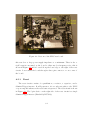
The XPIC test board. . . . . . . . . . . . . . . . . . . . . . . . . 63
ix
4.2
4.3
4.4
4.5
4.6
4.7
4.8
Bottom of the XPIC test board. . . . . . . . . . . . . . . . . . . .
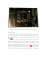
Top layer of the XPIC board without any components. . . . . . .
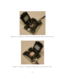
Another view of the test board showing the inside of the test socket.
The test board with an XPIC chip in position in the socket. . . .
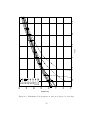
Maximum clock frequency at various voltages for each chip. . . . .
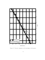
Current consumption at the maximum clock frequency. . . . . . .
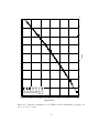
Current consumption at 50 MHz from the minimum operating
voltage to about 3.7 volts. . . . . . . . . . . . . . . . . . . . . . .
x
64
65
67
67
70
71
72
List of Tables
2.1
2.2
2.3
2.4
2.5
2.6
Special Function Register (SFR) memory map. . . . . . . . . . . .
The XPIC Instruction Set: Data Memory Operations . . . . . . .
The XPIC Instruction Set: Literal, Table and Control Operations
Timer Prescaler ratios for various TPS bit settings . . . . . . . .
Port E states at reset and the program that will be run. . . . . .
Serial EEPROM format used in booting the XPIC. . . . . . . . .
xi
11
14
15
24
27
29
Chapter 1
Introduction
This thesis describes the design, implementation and test of a PIC compatible [4] microcontroller. This controller was chosen as a test bench for a new
processor design flow based on a new high level representation of the design. To
enable a fair benchmark of the new methodology, the processor maintains binary
compatibility with the PIC standard [3] while providing a rich set of peripherals
and processor extensions. First, the processor has high performance, being designed as a 4-stage pipeline architecture. Second, the controller supports a small
set of instruction extensions which greatly improve table lookup performance
and make possible read/write access to program memory. Third, the controller
has two channels of high performance pulse rate modulation based digital to
analog conversion. (Pulse rate modulation has much better noise characteristics
at high speed than pulse width modulation, which is why it is used.) Fourth,
the controller has a set of timer and control peripherals adherent to the PIC
standard. Fifth, the controller has two high speed serial communication ports
for multi-Mb/s 2-wire communication capability. Finally, the contoller is designed to operate at 100+ MHz clock rates (in 0.5µm technology) and achieves
an IPC of nearly 1.0, making it the fastest processor of its type available. (It
has roughly 20x the native performance of a high speed commercial version from
Microchip[3] and nearly 2x the performance of the Ubicom (formerly Scenix)
1
version of the part[10]). This performance is partly enabled by execution out of
RAM versus EPROM or EEPROM storage, but is also partly due to the design
methodology.
There were several goals in this design project. First, we wanted to demonstrate a professional quality design constructed largely by direct synthesis. The
design had to be compatible with a commercial product in order to show that
a synthesis based flow could indeed compete with professional design in similar
technologies. We needed to show that the high level flow could be constrained
to construct a high performance and not just functionally correct design. Finally, we wanted to validate that design change, debugging and update could be
accomplished with ease in an applicative language based on extended regular expressions. The essential notion of the specification strategy is the identification
of desired execution sequences and direct implementation of the controller from
a non-deterministic specification format. This model allows for directed sequential optimization which helps to prevent critical path formation through the controller. This synthesis model is discussed in ”Clairvoyant: A Synthesis System for
Production-based Specification” [11]. An additional goal of the design is to construct a complete set of design views from very high level, RTL, gate-level, circuit
and layout level for a working practical design. These views are made available
via the web at: http://bears.ece.ucsb.edu/research-info/XPIC/index.html.
The design flow consisted of using Synopsys Protocol Compiler in a nontraditional way to synthesize a VHDL based controller. This controller comprised
the majority of the design. Additional portions of the design were manually
written in VHDL (these comprised the data-path, serial ports and some of the
peripherals). This VHDL model was simulated via Mentor Graphics’ Model
Sim tools and was synthesized via Synopsys Design Compiler. Chip assembly
and layout was done in Duet technology’s Epoch back end layout tools with
final verification, DRC and LVS using Mentor Graphics’ Designer Checkmate.
During the design process, a substantial portion of design work was devoted to
test features of the design, including built-in functional test in the ROM. Test
2
was built in at such a low level to enhance the probability of useful results from
the fabrication in case there had been a substantive design or fabrication error.
The ROM code also contains initialization and boot loader code for a two wire
I2 C interface to a serial EEPROM containing the desired program. This code
was instrumental in providing a base for testing the processor at high speeds and
for SCHMOO plotting of the fabricated chips. The ROM code was built using
a slightly extended gpasm assembler. Fabrication, wafer probe and packaging of
the die was performed by MOSIS.
There has been some previous work in designing hardware using high-level
specifications. First, there was a similar PIC design several years ago by Nandakumar Sampath at UC Santa Barbara that also used Synopsys Protocol Compiler to synthesize the processor core of a chip. While this chip only ran the
12-bit PIC instruction set and did not have interrupts or timers, it was used as
a base design in some of the early versions of the XPIC. Another example of
work in using high-level specifications is in a cycle-accurate simulator that uses
a high-level design specification [1]. Like Protocol Compiler, the language for
this tool was designed to make short, cycle-accurate specifications of a design;
although this tool was designed for simulation and not for synthesis. Other work
in [2] explored the use of operation-centric hardware descriptions in hardware
development. Here, the design is specified using a Term Rewriting System notation that effectively specifies a finite state machine. The language used here is
related to Frame Modeling Language, and has also been used to write complex
processors in a short specification.
3
Chapter 2
User Manual
2.1
XPIC Overview
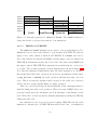
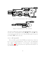
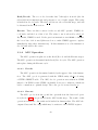
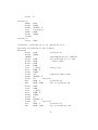
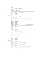
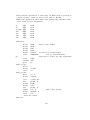
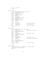
The XPIC is a microcontroller compatible with the Microchip PIC line of 14bit microcontrollers[4]. Figure 2.1 shows a simplified block diagram of the XPIC.
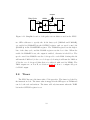
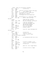
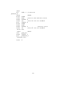
The pin diagram of the XPIC is shown in Figure 2.2. The XPIC is four stage
pipelined and can execute most instructions at the rate of one instruction per
clock. The XPIC has separate data and program memories. Program memory is
used primarily for executing program code, but it can be read and written by a
program using the table read/write mechanism. Data memory is used primarily
for general purpose data storage, although there are several control registers,
known as Special Function Registers (SFRs), in this space. Most XPIC data
instructions act on a working register, known as WREG, and either a literal
value or a data memory location. The XPIC has interrupt capability and can
accept interrupts from several sources.
There are 18 general purpose I/O pins on the XPIC. These pins can be
individually made inputs or outputs. Two 16-bit pulse rate modulators provide
D/A conversion capability. An 8-bit timer with a 7-bit programmable prescaler
is included. Two serial links are provided for high-speed communication with
other XPICs.
4
1k x 14
ROM
1k x 14
RAM
Addr
XPIC
Core
Port
E
PE1/SCL
PE0/SDA
Data In
Port
A
PA7
PA6
PA5
PA4
PA3
PA2
PA1
PA0
Port
B
PB7
PB6
PB5
PB4
PB3
PB2/INT
PB1/PRM2
PB0/PRM1
Data Out
Write Enable
Write Addr
Data Out
Read Addr
Data In
Reset
Clock
Vdd
Vss
Interrupt
Controller
PRM
1,2
Timer
S1 Out
Register
File
16x8 each
Serial
Links
1,2
S1 In
S2 Out
S2 In
Figure 2.1: Block diagram showing the major blocks of the XPIC.
5
N/C
Clock
Reset
Gnd
Vdd
Ser In 1
Ser Out 1
Gnd
Vdd
B0
B1
B2
N/C
9
8
11
10
13
12
14
15
16
17
19
18
20
N/C
Gnd
Vdd
B3
B4
Gnd
Vdd
B5
B6
B7
Gnd
Vdd
N/C
21
7
22
6
23
5
24
25
3
XPIC
26
4
2
27
1
52 pin LCC
28
29
52
51
30
50
31
49
32
33
48
47
N/C
Vdd
Gnd
A7
A6
A5
Vdd
Gnd
A4
A3
Vdd
Gnd
N/C
46
45
43
44
41
42
39
40
38
36
37
35
34
N/C
A2
A1
A0
Vdd
Gnd
Ser Out 2
Ser In 2
Vdd
Gnd
E2
E1
N/C
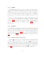
Figure 2.2: Pin diagram of the XPIC.
The ROM is used for booting the XPIC by loading a program from a serial
EEPROM and running it. The ROM has several helper functions to read and
write I2 C devices, perform multiplications, and to provide a cosine function.
There is also a self test routine in the ROM to assist in testing the XPIC.
2.2
Compatibility
The XPIC is designed to be compatible with the Microchip 14-bit PIC
microcontrollers[4]; however, there are differences. This section summarizes
these differences and was written primarily for those who are familiar with PICs.
6
2.2.1
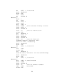
Program Memory
14-bit PICs have their entire program memory as built-in EPROM or Flash,
and most are programmed using special programming hardware controlled by
an external programmer [7](although some newer models can be programmed
from a running program[6]). The XPIC has a 1024 word program ROM and
a 1024 word program RAM. Programs are stored on an external 24LC32 serial
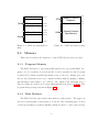
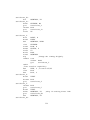
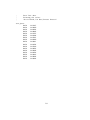
EEPROM and are executed from program RAM. Figure 2.3 shows the program
memory map. The ROM is used for booting the XPIC, which involves reading
a program from a serial EEPROM into RAM and then executing the program.
Section 2.10.4 describes the serial EEPROM boot process. It should also be
noted that program RAM can be loaded at any time, meaning a program can
be paged in and out of a serial EEPROM as needed.
2.2.2
Data Memory
The XPIC has only a single data memory page, as opposed to the 2-4 pages
in 14-bit PICs. The XPIC has 96 bytes of general-purpose data memory. The
data memory map for the XPIC is shown in Figure 2.4. The SFR (Special
Function Register) mapping has changed somewhat, the new SFR map is shown
in Table 2.1. Some of the notable differences are that the Digit Carry (DC) flag in
STATUS is not present (this was because of problems in getting an intermediate
carry signal), the PCLATH register is mapped to the upper bits of STATUS
(instead of having its own register), and the I/O port registers are in different
places.
2.2.3
Indirect Addressing
Indirect data memory addressing works the same way on the XPIC as it does
on other PICs. However, there is a known bug in the XPIC implementation:
whenever INDF is read or written immediately after an instruction that writes
7
FSR, INDF will still appear as the old address, not the new address. Adding
an instruction (such as a NOP) between the FSR write and the INDF access will
work around the problem.
2.2.4
Instruction Set
The XPIC instruction set is extremely similar to the 14-bit PIC instruction
set. The XPIC does not implement the SLEEP or CLRWDT instructions, these
instructions are treated like NOP. The TRIS and OPTION instructions are also not
implemented; MOVWF can be used as an alternative. The XPIC has three new
instructions: TBLRD, TBLRDT, and TBLWT. These instructions are used to read and
write the program memory and are discussed in Section 2.4.5.
2.2.5
Pulse Rate Modulators
The XPIC has a pair of pulse rate modulators. Pulse rate modulation performs a function similar to pulse width modulation, but the output is much
better suited for D/A conversion. See Section 2.7 for details on how to use the
pulse rate modulators.
2.2.6
Serial Links
The XPIC has a pair of serial links for communicating with other XPICs.
These links are point to point interfaces and transmit data at 1/16 of the clock
speed. See Section 2.9 for details on how to use the serial links.
2.2.7
ROM Software
There are several programs and functions available in the ROM to perform
tasks such as multiply, cosine, and serial EEPROM read/write. The ROM software is discussed in Section 2.10.
8
00h
RAM Start Vector 000h
SFR
RAM
Interrupt Vector
Reset Vector
Special Function
Registers
1Fh
20h
008h
009h
3FFh
400h
401h
RAM
General Purpose
Data Memory
ROM
7FFh
7Fh
Figure 2.3: XPIC program memory
map
2.3
Figure 2.4: XPIC data memory map
Memory
This section describes the memories on the XPIC and how they are used.
2.3.1
Program Memory
The XPIC has 1k×14 of program RAM and 1k×14 of program ROM. Program code for execution is read from the location specified by the Program
Counter (PC), which normally increments every clock cycle. During reset, the
PC is loaded with the reset vector, which is address 400h (beginning of ROM).
An interrupt causes 008h to be loaded to PC, which is the interrupt vector.
User programs are started at location 000h (discussed in Section 2.10.4). The
program memory map is shown in Figure 2.3.
2.3.2
Data Memory
The XPIC has 128 bytes in the data memory address space. The upper 96
bytes are general-purpose data memory locations. The remaining space is used
for the special function registers (SFRs), which are used to control and read the
9
status of the CPU and the integrated peripherals. The map of the data memory
space is shown in Figure 2.4. The map of SFRs is shown in Table 2.1. Some of
the CPU related SFRs are described below.
2.3.2.1
STATUS
The STATUS register holds the ALU status bits, the PCLATH bits, and
the Global Interrupt Enable (GIE) bit. The PCLATH bits are used in indirect
jumps (discussed in Section 2.3.3). The GIE bit is set to enable interrupts, or is
cleared to disable them. It is cleared upon entering an interrupt routine and is
restored from its previous state when the interrupt handler returns. The Carry
(C) and Zero (Z) bits are updated by many arithmetic and logic operations.
Writing to either of these bits with any instruction that otherwise affects either
of these bits will have the write disabled to these bits.
2.3.2.2
Option
The OPTION register contains several bits controlling various resources. The
Interrupt Edge Select bit (INTEDG) is used to select which edge will be detected
from the INT pin (port B, bit 2). The Timer Enable (T0EN) and Timer Prescaler
Select (TPSx) bits are discussed in Section 2.8. The Pulse Rate Modulator
Enable bits (PRM1EN and PRM2EN) are discussed in Section 2.7.
2.3.2.3
INT
The INT register holds the interrupt flags and interrupt enable bits. The interrupt flags are External Interrupt (EINT), Timer Interrupt (TINT), and Serial
Link Interrupt (SINT). The interrupt enable bits correspond to the interrupt flag
bits and are EEN, TEN, and SEN. Whenever an interrupt event occurs, the flag
for that interrupt is set in the INT register. If the enable bit for that interrupt
is set and the GIE bit (in STATUS) is also set, an interrupt will occur. The
flags must be cleared in software or else the interrupt will reoccur as soon as the
10
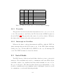
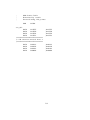
Addr Name
00h
INDF
Bit 7
Bit 6
Bit 5
Bit 4
01h
TMR0
Timer Register
02h
PCL
Lower 8 bits of Program Counter (PC)
03h
STATUS
PCLATH2
04h
FSR
1
PCLATH1
PCLATH0
OPTION
T0EN
INTEDG
PRM2EN
PRM1EN
INT
EEN
TEN
SEN
0
Bit 0
Z
0
C
TPS2
TPS1
TPS0
TINT
SINT
0
EINT
Unimplemented location, reads are undefined
09h
TBLATH
0Ah
TBLPTL
0
0
Read/Write buffer for upper 6 data bits of TABLE operations
Lower 8 address bits for TABLE operations
0
0
0
0
0Bh
TBLPTH
0Ch
PORTA
Read Port A pins, Write Port A Output Latch
0Dh
TRISA
Port A Data Direction Register
0Eh
OUTA
Read/Write Port A Output Latch
0Fh
PORTE
10h
PRM1H
11h
PRM1L
Lower 8 bits for Pulse Rate Modulator 1
12h
PRM2H
Upper 8 bits for Pulse Rate Modulator 2
13h
PRM2L
Lower 8 bits for Pulse Rate Modulator 2
14h
PORTB
Read Port B pins, Write Port B Output Latch
15h
TRISB
Port B Data Direction Register
16h
OUTB
Read/Write Port B Output Latch
17h
PRMSPEED
18h
RXBUF
Serial Link Receive Data Register
19h
TXBUF
Serial Link Transmit Data Register
1Ah
MSGLEN
1Bh
0
0
0
0
0
Upper 3 addr bits for TABLE ops
SCL
SDA
SCLT
SDAT
0
0
0
PRMSP2
PRMSP1
R1LEN0
T0LEN1
T0LEN0
R0LEN1
R0LEN0
TE0
T0
RE0
R0
READ
0
LK
CS
Upper 8 bits for Pulse Rate Modulator 1
0
T1LEN1
0
T1LEN0
0
R1LEN1
Unimplemented location, reads are undefined
STATREG
1Dh
1Fh
Bit 1
Unimplemented location, reads are undefined
08h
1Eh
Bit 2
Pointer for indirect data memory accesses
06h
07h
0
GIE
05h
1Ch
Bit 3
Accesses Data Memory location pointed to by FSR (Not a physical register)
TE1
T1
RE1
R1
Unimplemented location, reads are undefined
SCONTROL
0
0
MASK1
MASK0
Unimplemented location, reads are undefined
Unimplemented location, read as value specified or else undefined. Writes have no effect.
Table 2.1: Special Function Register (SFR) memory map.
11
interrupt is reenabled.
2.3.3
Indirect Jumps
The XPIC can perform indirect jumps through the PCL (program counter
low) register and the PCLATH (program counter latch high) bits in STATUS.
Reading PCL will read the lower 8 bits of the PC (the address of the next
instruction). Writing to PCL will write the result to the low 8 bits of the PC,
and the PCLATH value is written to the upper 3 bits of PC. This action causes
a jump to the new PC value and will cause the instruction to take three cycles.
2.3.4
Stack
The XPIC has an 8-level, 11-bit hardware return stack. The current PC
value is pushed onto this stack whenever the CALL instruction is executed. The
stack is popped to the PC whenever a RETURN or RETLW instruction is executed.
Unlike the PIC16C devices, the XPIC does not use this stack for interrupts or
the RETFIE instruction; there is a separate storage space for these events as
discussed in Section 2.5. There is no mechanism for detecting a stack overflow
or underflow. There is also no mechanism to manually push or pop values from
the stack.
2.3.5
Indirect Addressing
Indirect addressing to data memory is done by writing the desired address
to FSR, then reading or writing the data through INDF. INDF acts like the
register referenced by FSR. This can be used to read or write any data memory
address. When FSR is zero (the INDF address), INDF always reads as zero and
writes are made to the bit bucket. There is one known implementation issue
on the XPIC regarding FSR and INDF: writing FSR does not take immediate
effect. One instruction cycle is needed between a write to FSR and a read/write
12
through INDF. This was done because of chip area problems and performance
issues.
2.3.6
Table Read and Write
The table read/write system enables reads and writes to program memory
by a running program. There are three registers associated with the table mechanism: TBLATH, TBLPTL, and TBLPTH. TBLATH holds the upper 6 bits of
data for reading or writing. TBLPTL holds the lower 8 bits of the address for
TBLRD and TBLWT instructions. TBLPTH holds the upper 3 address bits. This
mechanism is described in detail in Section 2.4.5.
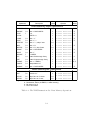
2.4
Instruction Set
The XPIC can execute 36 different instructions. The instruction set is summarized in Tables 2.2 and 2.3. Table 2.2 shows the instructions that read and
write data memory. Table 2.3 shows the literal, control, and table instructions.
2.4.1
Byte Instructions
The byte instructions are shown in Table 2.2 and operate on a data memory location and/or WREG. The general form is 00 iiii dfff ffff, where i
selects the instruction, d selects the destination for the result, and f selects a
data memory address to operate on. The destination (d) bit is clear to write
the result to WREG, and set to write the result to data memory. Some of the
byte instructions modify the Carry and Zero bits in STATUS, the affected bits
are shown in the far right column in Table 2.2. All byte instructions execute
in one clock cycle, except for DECFSZ and INCFSZ which take two clock cycles if
the result is zero. The execution pattern for single cycle instructions is shown
in Figure 2.5. The execution pattern for DECFSZ and INCFSZ when they cause a
skip is shown in Figure 2.6.
13
Mnemonic,
Operands
Description
Cycles
Opcode
Status
Data Memory Byte Operations
ADDWF
f, d
ANDWF
f
CLRF
1
00 0111 dfff ffff
dest = f AND WREG
1
00 0101 dfff ffff
f, d
dest = f + WREG
1
f=0
1
CLRW
WREG = 0
COMF
f, d
f, d
DECF
dest = f - 1
dest = f - 1, skip if zero
f, d
DECFSZ
f, d
INCF
1
dest = ~f
dest = f+1
f, d
INCFSZ
dest = f+1, skip if zero
f, d
IORWF
dest = f OR WREG
1
00 0011 dfff ffff
1,2
00 1011 dfff ffff
1
00 1010 dfff ffff
1,2
00 1111 dfff ffff
1
00 0100 dfff ffff
f, d Rotate f right through Carry
1
00 1100 dfff ffff
C
dest = f - WREG
1
00 0010 dfff ffff
C,Z
f, d Swap nibbles in f
1
00 1110 dfff ffff
1
00 0110 dfff ffff
dest = f XOR WREG
f, b Clear bit b in f
1
01 00bb bfff ffff
f, b Set bit b in f
1
01 01bb bfff ffff
1,2
01 10bb bfff ffff
f, b Skip if bit b in f is clear
BTFSS
1,2 01 11bb bfff ffff
f, b Skip if bit b in f is set
f : Data memory address (00h to 7Fh)
d : Destination Select (0=WREG, 1=data memory)
b : Bit select (0 to 7)
x : Don’t care value
Legend:
Table 2.2: The XPIC Instruction Set: Data Memory Operations
14
Z
Data Memory Bit Operations
BTFSC
Z
C
f, d
BSF
Z
00 1101 dfff ffff
BCF
Z
1
f, d
XORWF
Z
00 1001 dfff ffff
f, d Rotate f left through Carry
00 0000 1fff ffff
SWAPF
Z
00 0001 0xxx xxxx
1
SUBWF
f = WREG
f
RRF
Z
00 0001 1fff ffff
00 1000 dfff ffff
RLF
Z
1
MOVWF
dest = f
f, d
MOVF
C,Z
Z
Mnemonic,
Operands
Description
Cycles
Opcode
Status
C,Z
Literal Operations
ADDLW
ANDLW
IORLW
MOVLW
RETLW
SUBLW
XORLW
WREG = lit + WREG
1
11 111x kkkk kkkk
WREG = lit AND WREG
1
11 1001 kkkk kkkk
lit
lit
1
11 1000 kkkk kkkk
WREG = lit
1
11 00xx kkkk kkkk
WREG = lit, return from sub
1
11 01xx kkkk kkkk
WREG = lit - WREG
1
11 110x kkkk kkkk
WREG = lit XOR WREG
1
11 1010 kkkk kkkk
lit
lit
lit
lit
Z
WREG = lit OR WREG
lit
Z
C,Z
Z
Table Operations
TBLRD
Table Read
2
00 0000 0xxx 0100
Table Read using WREG
2
00 0000 0xxx 0101
Table Write
3
00 0000 0xxx 0110
TBLRDT
TBLWT
Control Operations
CALL
lit
Call Subroutine at lit
3
10 0kkk kkkk kkkk
GOTO
lit
Goto address lit
3
10 1kkk kkkk kkkk
NOP
No Operation
1
00 0000 0xxx 0000
RETFIE
Return from Interrupt
3
00 0000 0xxx 1001
RETURN
Return from Subroutine
3
00 0000 0xxx 1000
Legend:
k : Literal value; data or jump address
x : Don’t care value
Table 2.3: The XPIC Instruction Set: Literal, Table and Control Operations
15
Cycle 1
MOVWF
Cycle 2
MOVF
PRM1H
prod1,W MOVWF
Cycle 3
MOVF
PRM1H
prod1,W MOVWF
Cycle 4
MOVF
PRM1H
prod1,W MOVWF
Cycle 5
MOVF
Fetch
Read/Decode
Execute
PRM1H
prod1,W
Write
Figure 2.5: Execution pattern for byte, bit, and literal instructions.
Cycle 1
btfss
Cycle 2
goto
Cycle 3
movwf
TMR0, 6
aud_w1 btfss
PRM2L goto
Cycle 4
TMR0, 6
aud_w1 btfss
movwf
PRM2L
Cycle 5
TMR0, 6
Skipped
movwf
PRM2L
Cycle 6
btfss
Skipped
movwf
Fetch
Read/Decode
Execute
TMR0, 6
PRM2L
Write
Figure 2.6: Execution pattern for DECFSZ, INCFSZ, BTFSS, and BTFSC when a
skip is triggered. The BTFSS instruction will cause the GOTO aud w1 instruction
to be skipped.
2.4.2
Bit Instructions
The bit instructions are shown in Table 2.2 and operate on a bit in a data
memory location. The general form is 01 iibb bfff ffff, where i selects the
instruction, b selects the bit, and f selects a data memory address to operate
on. All bit instructions execute in one cycle, except for BTFSC and BTFSS which
take two clock cycles if the selected bit is clear or set respectively. The execution
pattern for single cycle bit instructions is shown in Figure 2.5. The execution
pattern for BTFSS and BTFSC when they cause a skip is shown in Figure 2.6.
2.4.3
Literal Instructions
The literal instructions are shown in Table 2.3 and operate on WREG using
a literal value provided in the instruction. The general form is 11 iiii kkkk
16
cos_zero
Cycle 1
GOTO
Cycle 2
XORLW
Cycle 3
MOVWF
Cycle 4
BCF
0x80 GOTO
cos_zero
PORTA XORLW
Cycle 5
0x80 GOTO
Flush
STATUS,C
BCF
cos_zero
Flush
Flush
STATUS,C
Cycle 6
GOTO
BCF
Flush
Flush
STATUS,C
Cycle 7
BCF
Flush
Read/Decode
Execute
cos_zero
STATUS,C
Write
Figure 2.7: Execution pattern for writes to PCL and the GOTO, CALL, and RETURN
instructions. The GOTO instruction causes the next two instructions to be flushed.
kkkk, where i selects the instruction and k is an 8-bit literal value to be used in
the operation. Some of the literal instructions modify the Carry and Zero bits
in STATUS, the affected bits are shown in the far right column in Table 2.3. All
literal instructions execute in one cycle, except for RETLW which takes three. The
execution pattern for literal instructions except for RETLW is shown in Figure 2.5.
2.4.4
Control Instructions
The control instructions are shown in Table 2.3. The NOP instruction performs
no operation and executes in one cycle. The other instructions, as well as RETLW
and any instruction that writes to PCL, all cause a jump and take three cycles
to execute. The execution pattern for these instructions is shown in Figure 2.7.
2.4.5
Table Instructions
The table instructions are shown in Table 2.3. These instructions are used to
read and write program memory. These instructions use the WREG, TBLATH,
TBLPTL, and TBLPTH registers.
17
Cycle 1
TBLRDT
Cycle 2
MOVWF
Cycle 3
Cycle 4
prod1 TBLRDT
Table Read Data
BCF
STATUS,C
Cycle 5
MOVWF
prod1 TBLRDT
Table Read Data
BCF
STATUS,C
Cycle 6
MOVWF
prod1 TBLRDT
Table Read Data
BCF
STATUS,C
Cycle 7
MOVWF
Read/Decode
Execute
prod1
Table Read Data
BCF
Fetch
STATUS,C
Write
Figure 2.8: Execution pattern for TBLRD and TBLRDT. The TBLRDT instruction
causes the fetch to read user data instead of an instruction.
2.4.5.1
TBLRD and TBLRDT
The TBLRD and TBLRDT instructions are used to read program memory. For
TBLRD, the lower 8 bits of the address to read is taken from TBLPTL, and the
upper 3 bits of the address is taken from TBLPTH. For TBLRDT, the lower 8
bits of the address are taken from WREG, and the upper 3 bits are taken from
TBLPTH. Both instructions place the lower 8 bits of the data read in WREG and
the upper 6 bits in TBLATH. These instructions normally take two clock cycles
to execute. The execution pattern for these instructions is shown in Figure 2.8.
Note that the instruction immediately after the table instruction is executed:
this means that if the table operation is followed by an instruction that causes
a jump (like CALL or RETURN), the table operation will effectively take one clock
cycle. This is because the pipeline bubble created by the table read operation
will be absorbed by the pipeline flush of a jump operation.
There are a few known bugs in this mechanism. First, interrupts must be
disabled during the table read operation. This is because WREG will not be
properly backed up by the interrupt logic if an interrupt occurs during a table
read. This can be worked around by disabling interrupts (clearing the GIE bit)
during the table read.
One instruction cycle is needed between writing TBLPTH and the table
instruction, otherwise the old TBLPTH value will be used. Also, one instruction
18
Cycle 1
TBLWT
Cycle 2
BSF
OUTB,2 TBLWT
Cycle 3
Table Write Data
Cycle 4
Table Write Data
Cycle 5
CLRF
TMR0
Cycle 6
BSF
OUTB,2 TBLWT
Table Write Data
Table Write Data
CLRF
TMR0
Cycle 7
OUTB,2 TBLWT
BSF
Table Write Data
Table Write Data
CLRF
TMR0
Cycle 8
BSF
OUTB,2
Table Write Data
Table Write Data
CLRF
Fetch
Read/Decode
Execute
TMR0
Write
Figure 2.9: Execution pattern for TBLWT. Since program memory is being written,
instruction fetches cannot take place.
cycle is needed between the table instruction and a read of TBLATH, otherwise
the old TBLATH value will be read. (WREG is updated immediately after a
table instruction.) For TBLRD, TBLPTL must either be written immediately
before the TBLRD instruction, or there must be at least two instruction cycles
between the write to TBLPTL and the TBLRD instruction. (TBLRDT does not
have this problem, as it does not use TBLPTL.)
2.4.5.2
TBLWT
The TBLWT instruction is used to write program memory. The low 8 bits
of the address to write is taken from TBLPTL, and the upper 3 bits of the
address is taken from TBLPTH. The low 8 bits of the value to write is taken
from WREG, and the upper 6 bits are taken from TBLPTH. This instruction
normally takes three clock cycles to execute. The execution pattern for TBLWT
is shown in Figure 2.9. Note that the instruction immediately after the TBLWT
instruction is executed: this means that if the table operation is followed by
an instruction that causes a jump (like CALL or RETURN), the TBLWT operation
will effectively take one clock cycle. This is because the pipeline bubble created
by the table write operation will be absorbed by the pipeline flush of a jump
operation.
19
There are several known bugs with TBLWT, One instruction cycle is needed
between writing TBLPTH or TBLATH and the TBLWT instruction, otherwise
the old TBLPTH or TBLATH value will be used. TBLPTL must either be
written immediately before the TBLWT instruction, or there must be at least two
instruction cycles between the write to TBLPTL and the TBLWT instruction.
Also, skip instructions will not work immediately after a TBLWT instruction, as
the skip will simply not be taken.
2.5
Interrupts
Interrupts occur whenever the GIE bit in STATUS is set and both an interrupt flag and its corresponding interrupt enable bit in the INT register are both
set. Interrupts always take three clock cycles between when the interrupt event
occurs and when the first instruction of the interrupt handler is executed. Whenever an interrupt occurs, the PC, STATUS, and WREG values are all saved to
shadow registers and do not have to be backed up by the user. The PC is then
set to 008h (the interrupt vector), and the GIE bit in STATUS is cleared.
An interrupt routine is ended with the RETFIE instruction. This instruction restores the previous values of PC, STATUS, and WREG from the shadow
registers.
2.6
I/O Ports
There are 18 general purpose I/O pins on the XPIC. Each pin can be used
as either an input or an output. Ports A and B have 8 pins each, while Port E
has 2 pins.
20
2.6.1
Port A
There are three SFR addresses for Port A: PORTA, OUTA, and TRISA.
These are shown in Table 2.1. The PORTA address writes to the Port A Output
Latch and reads the actual pin state. The OUTA address reads and writes the
Port A Output Latch. The TRISA address reads and writes the Port A Data
Direction Register. Setting a bit in this register makes the corresponding pin an
input while clearing a bit makes a pin an output. This register is set to all ones
during reset.
2.6.2
Port B
There are three SFR addresses for Port B: PORTB, OUTB, and TRISB.
These are shown in Table 2.1 and have the same function as the Port A SFRs
of the similar name. Port B also has the pulse rate modulator outputs and the
external interrupt input.
2.6.2.1
PRM Output
Pins 0 and 1 of Port B are also the pulse rate modulator outputs for PRM1
and PRM2 respectively. The pulse rate modulators are discussed in detail in
Section 2.7. To use the PRMs, the pin must be configured as an output in
TRISB, and the output value must be set to low (otherwise the output will be
held high).
2.6.2.2
External Interrupt Input
Pin 2 of Port B is the external interrupt input. The interrupt is edge triggered. The edge is selectable through the INTEDG bit in the OPTION register:
setting this bit will trigger on a rising edge of this pin, while clearing this bit will
trigger on a falling edge. When the edge is detected, the EINT bit in the INT
register is set. This will cause an interrupt if the EEN and GIE bits are set.
21
1/2
1/4
3/4
1/3
2/7
Figure 2.10: Example of pulse rate modulator output for various duty cycles.
2.6.3
Port E
Port E is a two pin port used primarily to read and write I2 C serial EEPROMs
and to determine the boot mode. There is one SFR address for Port E: PORTE.
The bits in this register are named after the two I2 C signal lines: SDA and SCL.
The SDA and SCL bits read the pin states and write the output latch. The
SDAT and SCLT read and write the data direction latch. Writing a one to one
of these bits makes the pin an input, while writing a zero makes the pin an
output.
2.7
Pulse Rate Modulators
Pulse rate modulation generates an output with a desired duty cycle. The
output is transitioned as quickly as possible, placing most of the noise generated
by the modulation near one half of the clock frequency. This is easy to filter out
using a low pass filter, making pulse rate modulation suitable for D/A conversion.
Some pulse rate modulation examples are shown in Figure 2.10. The hardware
to do pulse rate modulation is also rather simple, it is shown in Figure 2.11.
The XPIC has two 16-bit Pulse Rate Modulators (PRMs). Each PRM has
22
Output
Duty Cycle
Adder
Accumulator
Carry
16
16
16
Figure 2.11: Simplified version of the pulse rate modulators used in the XPIC.
two SFR addresses to specify the 16-bit duty cycle (PRMxL and PRMxH),
one enable bit (PRMxEN) in the OPTION register, and one speed control bit
(PRMSPx) in the PRMSPEED register. The PRMxH register sets the high 8
bits of the duty cycle, and the PRMxL register sets the low 8 bits. When the
enable bit PRMxEN is set, the output is enabled, otherwise it is held low. The
speed control bits PRMSPx set the clock speed for each PRM. Setting this bit
will run the PRM at 1/2 the core clock speed, clearing it will run the PRM at
1/510 the core clock speed (this divisor is achieved with an 8-bit LFSR). The
PRM outputs are on Port B, see Section 2.6.2.1 for how to configure the port
for PRM output.
2.8
Timer
The XPIC has an 8-bit timer with a 7-bit prescaler. The timer is clocked by
the instruction clock. The timer value is mapped in the SFR space as TMR0 and
can be both read and written. The timer will only increment when the T0EN
bit in the OPTION register is set.
23
TPS2 TPS1 TPS0 Timer Prescale Ratio
0
0
0
1:1
0
0
1
1:2
0
1
0
1:4
0
1
1
1:8
1
0
0
1:16
1
0
1
1:32
1
1
0
1:64
1
1
1
1:128
Table 2.4: Timer Prescaler ratios for various TPS bit settings
2.8.1
Prescaler
The prescaler can decrease the timer increment rate by 1, 2, 4, 8, 16, 32, 64,
or 128. The amount is controlled by the TPS bits in the OPTION register as
shown in Table 2.4. The prescaler value cannot be read by software. Whenever
the timer value is written, the value in the prescaler is cleared.
2.8.2
Interrupt on Overflow
Whenever the timer overflows (increments from FFh to 00h) the TINT bit
(timer interrupt flag) in the INT register is set. If the TEN (timer interrupt
enable) bit is set, and the GIE bit in STATUS is also set, an interrupt will
occur. The TINT bit must be cleared in software.
2.9
Serial Links
The XPIC has two bidirectional serial links, which are point to point serial
interfaces. The serial links can be used to communicate with other XPICs. Each
serial link consists of two unidirectional lines which transmit at a rate of 1/16
the core clock speed. The lines in either direction are independent, so it is
possible to transmit and receive simultaneously for full-duplex operation, as well
as communicate on each serial link independently.
24
2.9.1
Protocol
The protocol defined on these serial links is that a processor may transmit
one packet at a time, each containing a two bit header and eight bits of data.
Synchronization is done by the receiver upon seeing the first bit of the packet
header. The receiver must reply to each packet received with a two bit acknowledgement pulse before the transmitter can send the next packet. At full speed,
it takes approximately 14 serial clock cycles or 224 processor clock cycles to
complete the transmission and acknowledgement of one packet. Thus, when the
processor is running at 90 MHz, the speed of the serial links is 400 KB/s or 3.2
Mbps.
If a processor transmits a packet along a serial link, it expects to receive an
acknowledgement within 16 serial clock cycles. If it does not receive acknowledgement within this time, the transmission is considered a failure. At this
point, the byte is dropped, an error signal is sent to the processor, and the next
packet is readied for transmission. Retransmission in the presence of errors must
be done manually. Some instances in which a transmission error may occur is
if there is noise on the line, causing the receiver to not interpret the incoming
packet correctly, or if the receiver cannot accept the data because of a full buffer.
The second condition will also cause an error signal to be sent to the processor
on the receiver side.
Internally, each end of each line in the serial link is connected to a 4-byte
FIFO. Each link can be programmed to send or receive messages of 1 to 4 bytes
of data before signalling the processor. Such signalling can be done with an
interrupt or by polling a bit in the serial link status register. Thus, it is possible
to send or receive multi-byte packets with no processor intervention.
2.9.2
Transmission
A byte is transmitted by selecting the link with the LK bit in SCONTROL
(clear for link 0, set for link 1), and writing a byte to the TXBUF register. The
25
TxLEN bits in the MSGLEN register select the number of bytes that will be
sent before the Tx bit in STATREG is set. Up to four bytes can be queued for
transmission. Writing more bytes will result in lost data (and is not reported).
If an error occurred in transmission, the TEx bit is set. Both Tx and TEx must
be cleared by the program.
2.9.3
Reception
A byte is received by selecting the link with the LK bit in SCONTROL (clear
for link 0, set for link 1), reading the byte from RXBUF, and writing a one to
the READ bit in SCONTROL. (Writing a one to the READ bit was needed to
finish a read because the XPIC performs speculative reads.) The RxLEN bits
in the MSGLEN register select the number of bytes that will be received before
the Rx bit in STATREG is set. Up to four bytes can be received before the
input FIFO overflows. A receive FIFO overflow will cause the REx bit to be set.
Errors in reception can also cause the REx to be set. Both Rx and REx must
be cleared by the program.
2.9.4
Interrupts
The serial links can generate an interrupt whenever a bit in STATREG is
set. To use these interrupts, the GIE bit in STATUS must be set, the SEN bit
in INT must be set, and the MASKx bits for the desired serial links must be
set. The MASKx bits select which serial links interrupts will be enabled for. An
interrupt will occur whenever the enable bits are set and any of the Tx, TEx,
Rx, or REx bits in STATREG are set. To clear an interrupt, first the flags in
STATREG must be cleared, then the SINT bit in INT must be cleared.
26
Port E.1 Port E.2
Program to Run
SCL
SDA
Low
Low
Self Test
Low
High
Sine Wave Generation
High
X
Boot from Serial EEPROM
Table 2.5: Port E states at reset and the program that will be run.
2.9.5
Loopback
Setting the CS bit in SCONTROL will connect the transmit line of each
serial link to the receive line of the other serial link. This is done entirely on
the XPIC. Any data sent from one serial link is received by the other serial link.
Clearing the CS bit will return the serial links to their normal state. This feature
was used for testing the serial links in the ROM Self Test (Section 4.1.1).
2.10
ROM Software
The XPIC ROM contains several programs for testing and booting, as well
as several functions to make programming the XPIC easier.
2.10.1
Initialization
When the XPIC comes out of reset, it starts executing code at the beginning
of ROM. The XPIC has a short (12 words) initialization routine here that resets
some of the registers and starts the desired program. The program to run can
be either Self Test (Section 2.10.2), Sine Wave Generation (Section 2.10.3), or
Serial EEPROM Boot (Section 2.10.4). The program to start is selected by the
Port E state immediately after Reset. The Port E states and the program that
will be run is shown in Table 2.5.
27
2.10.2
Self Test
The Self Test program is a series of programs to test most of the internal
features of the chip. This is discussed in detail in Section 4.1.1.
2.10.3
Sine Wave Generation
This program uses the cosine function (Section 2.10.5.4) to generate sine
waves on the two pulse rate modulators. The first PRM has a single sine wave
at full amplitude running with a frequency of fclk /32768. The second PRM
has two sine waves digitally mixed together each at half amplitude and with
frequencies of fclk /32768 and fclk /163840. This program is 47 words long, not
including the cosine function or table. The sine wave output can be viewed with
an oscilloscope through a low pass filter connected to the PRM pin.
2.10.4
Boot (Serial EEPROM)
This program reads a program from a serial EEPROM connected to Port E,
saves it to the program RAM, and executes the program. The serial EEPROM
must be compatible to a 24LC32 and it must be configured to address zero [5].
(It is possible to have other I2 C devices or other serial EEPROMs connected
to Port E; only a serial EEPROM with address zero can be read by the boot
routine.) The serial EEPROM must have a weak pullup on the SDA line (this
is a requirement for any I2 C implementation), but SCL is fully driven by the
XPIC and a pullup resistor is only needed for boot mode selection.
A program on a serial EEPROM must be stored in the format shown in
Table 2.6. The first byte (I2 C speed) sets the I2 C bit rate. The bit rate is
approximately
bit rate =
fclk
4120 − 16n
where n is the I2 C speed value. Initially, the bit rate is set to zero, the slowest
speed possible. This was done to minimize boot times while keeping speed
28
Address
0000h
0001h
0002h
0003h
0004h
..
.
Value
ssssssss
00dddddd
dddddddd
00dddddd
dddddddd
..
.
Description
I C speed
High 6 bits of program RAM address 0
Low 8 bits of program RAM address 0
High 6 bits of program RAM address 1
Low 8 bits of program RAM address 1
..
.
2n + 1
2n + 2
2n + 3
2n + 4
00dddddd
dddddddd
01xxxxxx
xxxxxxxx
High 6 bits of program RAM address n
Low 8 bits of program RAM address n
End of transfer byte
User defined data (continues to end of device)
2
Table 2.6: Serial EEPROM format used in booting the XPIC.
compatibility at a maximum. Next, pairs of bytes are read from the serial
EEPROM and loaded into program RAM starting at address 0. This is done
with the program load function (Section 2.10.5.1). Data after the end of transfer
byte is not used during boot and can contain user data.
2.10.5
Helper Functions
There are several other functions that are included in the ROM that are
likely to be used by a user program. There are functions to read and write serial
EEPROMs, perform multiplications, and find the cosine of a value.
2.10.5.1
Serial EEPROM routines
These are high-level routines to read and write the serial EEPROM [5]. There
are three functions: program load, data load, and data save. These functions all
use the I2 C routines (Section 2.10.5.2).
Program Load (Address 6CCh) This function is used by the serial EEPROM
boot program (Section 2.10.4) and reads in byte pairs from a serial EEPROM to
program RAM. This function reads the high 6 bits, then the low 8 bits. For the
29
first byte of a pair, bit 6 is normally cleared. When this bit is set, this function
stops the I2 C connection and returns to the calling program. This function
assumes that the serial EEPROM is ready to be read, and that TBLPTL and
TBLPTH contain the starting address to write.
Data Load (Address 6BBh) This function reads bytes from the serial EEPROM and writes them to data memory starting at the address pointed to by
FSR. The number of bytes to read is equal to the value in data memory address 24h (prod0). After the data is read, the I2 C connection is stopped and the
function returns. This function assumes that the serial EEPROM is ready to be
read.
Data Save (Address 6B3h) This function reads bytes from data memory
(starting at FSR) and writes them to the serial EEPROM. The number of bytes
written is equal to the value in data memory address 24h (prod0). After the
data is written, the I2 C connection is stopped and the function returns. This
function assumes that the serial EEPROM is ready to be written. Note that
most (if not all) serial EEPROMs can only write to one page at a time, this
restriction must be handled by the calling program.
2.10.5.2
I2 C Functions
The I2 C functions perform the basic I2 C functions: start, restart, stop, byte
read, and byte write. These functions are used by all ROM routines that deal
with a serial EEPROM [5]. Four data memory locations are used by these
functions. Location 20h is cleared by I2 C delay, which is used by all of the I2 C
functions. Location 23h is cleared by the byte read and byte write functions.
Location 21h, known as iic delay val, sets the I2 C bit rate to
bit rate =
fclk
4120 − 16n
30
where n is the value in iic delay val. Location 22h, known as iic rw val, contains
the value to write to or read from the I2 C bus. Also, the carry flag in STATUS
contains the acknowledge bit to write or that was read.
I2 C Start and Restart I2 C Start (Address 6DBh) is used to begin an I2 C
transfer. An I2 C start is defined as a high-to-low transition on the SDA line
while SCL is high. I2 C Restart (Address 6DAh) is used to send a new control
byte when the I2 C bus is active. It does the same thing as I2 C start except that
a delay is added to the beginning to meet bus timing constraints.
I2 C Stop I2 C Stop (Address 6EAh) is used to end an I2 C transfer. An I2 C
stop is defined as a low-to-high transition on SDA while SCL is high.
I2 C Byte Read I2 C Byte Read (Address 71Ah) reads a byte from the I2 C
device on Port E. The data is written to iic rw val (22h). This function also
sends the acknowledge bit; this must be supplied in the carry flag. Data memory
location 23h is cleared by this function.
I2 C Byte Write I2 C Byte Write (Address 711h) writes a byte to the I2 C
device on Port E. The data to be written is taken from iic rw val (22h). This
function also gets the acknowledge bit; it is stored in the carry flag. Data memory
location 23h is cleared by this function.
I2 C Delay This function (Address 6D5h) generates the delays needed for I2 C
bus operation and is used by all of the other I2 C functions. This function uses
iic delay val (21h) to set the delay. The delay is 1030 − 4n clock cycles long,
where n is the value of iic delay val. The value in iic delay val is preserved by
this function, while data memory location 20h is cleared.
31
2.10.5.3
8x8 Multiply
(Address 74Bh) This function takes two 8-bit values, one in WREG and
the other in value0 (data address 23h), and multiplies them (both values are
considered to be unsigned). The product is written to prod0 (high byte, data
address 24h) and prod1 (low byte, data address 25h). This function uses the
right-shift algorithm and the loop is completely unrolled. It takes 37 clock cycles
to execute (plus the call to this function) and is 35 words long. There is a known
bug in this function in that if the carry bit is set and bit 0 of value0 is clear,
erroneous values may be produced. This can be worked around by making sure
carry is clear before calling this function.
2.10.5.4
Cosine Function
(Address: 72Ch, 8-bit; 72Dh, 9-bit) The cosine function reads an 8- or 9-bit
value and returns the cosine of this value in prod0 (high byte, data address 24h)
and prod1 (low byte, data address 25h). For 8-bit values, the function returns:
value × π
prod0 : prod1 = cos
128
!
× 32766
where value is the value in value0 (data address 23h). For 9-bit values, the
carry bit functions as the LSB below value0. The value is returned in two’s
complement form in the range −32766 to 32766 (which are equivalent to −1 and
+1 respectively). This function uses the cosine table (Section 2.10.7) to obtain
cosine values.
2.10.6
User Text
This is a small (17 words) block of memory which contains the text “Scott
Masch,Jon Hsu,Forrest Brewer” in packed ASCII format at address 76Eh. These
were the three primary people involved in designing the XPIC.
32
2.10.7
Cosine Table
This is a 128-entry quarter cosine table located between addresses 780h and
7FFh in the ROM. It is used by the cosine function (Section 2.10.5.4).
33
Chapter 3
XPIC Design
3.1
3.1.1
Design Methodology
Hardware
The processor core of the XPIC was designed using Synopsys Protocol Compiler [9], which is a high level synthesis tool that uses a regular expression like
input syntax and can generate VHDL, Verilog, or C output. The language used
in Protocol Compiler will be discussed in more detail in Section 3.2. Everything
was converted into a netlist and technology mapped using Synopsys Design Compiler. Layout, routing, static timing analysis, and module building (for ROMs,
RAMs, etc.) was done by Epoch from Cascade Design Automation (no longer
in existence). Most of the simulation was performed using Model Sim. The
boot code was tested using a serial EEPROM model generated with Synopsys
MemPro. Finally, DRC and LVS checking was performed with Mentor Graphics
CheckMate.
3.1.2
Software
The ROM code and other test programs were written in assembly and were
assembled using GPASM. GPASM is a GPL’d assembler for PICs, and was used
34
with the XPIC with no modification aside from a special include file. This include
file was needed to set the memory mapping and to add the table instructions.
There were several other programs that were written (in C) to create the ROM.
One program took the output of GPASM and generated the ROM image file for
Epoch. Another took the output of GPASM and generated a serial EEPROM
boot image.
3.2
Frame Modeling Language
Frame Modeling Language (FML)[8] is a regular expression based language
used to specify control structures. While FML has some characteristics (like
registers and I/O ports) common to other HDLs such as VHDL or Verilog, FML
has an advantage over other HDLs in that control mechanisms can be written
and modified easily. One example of a modification of the XPIC will be described
in Section 3.4, where the TBLWT timing was changed.
FML can be compiled into Verilog, VHDL, and C. A simple example of FML
is shown in Figure 3.1. This example detects the sequence “1101” on a, then
sets b high. The following sections describe how FML works.
3.2.1
Frames
Frames are roughly analogous to functions in other languages such as C.
Initially, the top level frame receives a single token immediately after reset. This
token then gets passed to the terminals (these are surrounded by [ and ]) in
the frame. When a terminal receives a token, it tests the condition defined in
the brackets, and if the condition is true it performs any actions associated with
it and passes the token in the next clock cycle. The two simplest terminals are
[0] (which absorbs a token and otherwise does nothing) and [1] (which always
passes a token and does the associated actions). The condition can be more
complicated: the example in Figure 3.1 tests the state of a in its terminals.
35
frame Top_example
{
repeat(+)
{
// Generate an infinite supply of tokens
{ [1] }
// Detect the sequence "1101" on a, set
//
b when sequence detected
{
[a == "1"]
[a == "1"]
[a == "0"]
[a == "1"]
set(b);
}
}
}
Figure 3.1: A simple example of FML
Terminals are always executed in sequence within a block (surrounded by {
and }). However, it is possible to have multiple blocks, which is two or more
blocks adjacent to each other. This is also known as an alternative block. In this
case, a token that reaches the first block will enter all of the blocks. Whenever
any of the blocks returns a token, a token is passed from the bottom of the last
block. The example in Figure 3.1 has two blocks within the repeat block.
It is possible for a design to have multiple frames. This is much like having a
program with multiple functions: one top level function can call other functions,
and these functions can call other functions, and so on. In FML, another frame
is called by simply using its name followed by a semicolon. This called frame
behaves like the code from the called frame was placed where the call was made.
The XPIC uses this primarily to help keep the code readable. The top frame of
the XPIC code in Figure 3.2 shows how other frames are called.
36
3.2.2
Actions
Actions are often associated with terminals (although the default action list
also has actions). They can be data movement operations, setting or clearing
of bits, or conditional operations. The syntax used is very similar to that of
VHDL or Verilog, and should be self explanatory. The only tricky part is the if
operator. Its syntax is if(cond ,then,else). Basically, if the condition cond is
true, the action then is performed, otherwise the action else is performed.
3.2.3
Repeats
The repeat operator will repeat as long as the condition within the block is
true. A token passed to a repeat block will enter the block. If and when the
block returns a token, the repeat block will pass a token and pass another token
to the beginning of the block. There are several different versions of repeat.
repeat (+) will only pass a token whenever the block inside it returns a token.
repeat (*) will both pass a token whenever the block inside it returns a token
and will immediately pass the initial token through immediately (also known as
an optional repeat). In the example, the repeat block is used to generate an
infinite supply of tokens.
The interrupt logic of the XPIC also uses the repeat operator to wait for a
condition to become true. The code in Figure 3.15 shows repeat (*) operator
being used to wait for an interrupt event.
3.2.4
Other Features
FML has other features that have counterparts in other languages such as
VHDL or Verilog. There are I/O ports and variables in FML. Default actions
(and reset actions) are always performed and behave like operations in VHDL
or Verilog. There are also expressions, they behave like the #define directive
in C. These features are discussed in the comments in the XPIC FML source in
37
frame Top
{
//Pipelined version of a PIC16C6X.
{
repeat (+)
{
{ data_hazards; }
{ execute; }
{ [1] }
}
}
{ interrupt; }
}
Figure 3.2: Top level FML frame for the XPIC
Appendix A.
3.3
XPIC Core
The XPIC core is written as a combination of default actions and frames.
Default actions are used extensively in the XPIC for optimization reasons (mostly
to eliminate unneeded reset logic). The top level frame for the XPIC is shown in
Figure 3.2. This frame passes a single token to the interrupt frame (discussed
in Section 3.3.14), and an infinite string of tokens to the data hazards frame
(Section 3.3.6) and the execute frame (various places). The entire FML source
of the XPIC is shown in Appendix A. The following sections describe the details
of how the XPIC works and how it was written.
3.3.1
Pipeline Flags
There are several pipeline flags that are used to control if an instruction is
executed. These are do1, do2, and x2. do1 is normally set but can be cleared to
stop execution of the instruction currently in the fetch stage. Clearing do1 will
38
PC
11 bit register
TBLPTR
11 bit register
0
read
addr Program data
1
Memory
ir1
14 bit register
pmem_addr_con
Figure 3.3: The Fetch hardware.
clear do2, x2, and pmem addr con in the next cycle. x2 (execute 2) is normally
set but can be cleared to prevent execution of the instruction currently in the
read/decode stage. do2 is normally the same as x2 and is used by the interrupt
logic (Section 3.3.14) to determine if an instruction would have been executed.
A fourth flag, pmem addr con, is set by the table instructions, but is cleared by
any instruction that clears x2.
3.3.2
Fetch
A block diagram of the Fetch stage is shown in Figure 3.3. When the
pmem addr con flag is clear (normal case), the instruction at the PC (Program
Counter) address is read and latched into ir1 (instruction register 1). The Program Counter is usually incremented, although there are several events (such
as interrupts and jumps) that will cause other values to be written to the Program Counter. When pmem addr con is set (table read or write), the data at
TBLPTR is read and latched into ir1.
3.3.3
Data Read
Most operation involving data (except moves) have two operands. These two
operands are generated over the Read cycle and part of the Execute cycle. These
two operands are fed to the ALU during the Execute stage. ALU operand A is
either a value from data memory or a literal value. ALU operand B is either
WREG or a value from the 3-to-8 decoder.
39
3.3.3.1
ALU Operand A
The first ALU operand comes from either the low 8 bits of the instruction
(literal instructions) or from a data memory location (bit and byte data memory
instructions). A block diagram of this mechanism is shown in Figure 3.4. This
read operation is split between the Read/Decode cycle and the Execute cycle.
Read/Decode First, the read address is calculated. Normally this will be the
low 7 bits of the instruction, but if the read is from INDF (address 00h) the actual
read address will be taken from FSR. This is done with the two NOR/MUX pairs
in Figure 3.4. The lower NOR/MUX pair performs an abbreviated version of
this calculation by testing only the upper four bits of the address. This is only
used for data memory reads outside of the core, which begins at address 0Ch.
The result of this read is stored in register a.
The upper NOR/MUX pair performs the full calculation and is the real read
address (also known as address1). This value is saved in address2 and is used for
local reads (addresses 01h to 0Bh, not including 04h (STATUS)). By default, the
result of this read is stored in register alt. If the instruction currently writing
back is writing to the address we are reading (address1 equals dmem waddr),
the data in dmem wdata is stored in register alt. If the instruction is a literal
instruction (upper bit of instruction is a one), a MOVWF instruction (needed for
simulation because of unknown propagation problems), or a CLRx instruction
(CLRW or CLRF, also needed for simulation), the lower 8 bits of the instruction
from ir1 are stored in register alt.
The alu a sel bits are also set in this stage. This will be discussed in the next
section.
Execute There are four possible sources for the first ALU operand: register a, register alt, STATUS, and dmem wdata. The value to use is selected by
the alu a sel register, which is set during the Read/Decode cycle. By default,
alu a sel is set to use register alt as the operand source. If the read was from
40
7:0
6:0
6:0
ir1
14 bit register
FSR
7 bit register
7:0
6:0
0
6:3
6:0
6:0
10
register_alt
8 bit register
00
3:0
1
0
7:0
Local
read Registers read
addr
data
dmem_wdata
8 bit register
7:0
alu_a_sel
2 bit register
6:0
address2
7 bit register
Data
7:0
read Memory read
addr
data
register_a
8 bit register
6:0
1
status
return
01
11
Status
6 bit register
Figure 3.4: Read mechanism for ALU operand A.
8
00
7:0
ir1
14 bit register
9:7
3-to-8 Decode
WREG
8 bit register
01 8
8
decode_latch
8 bit register
alu_b_sel
2 bit register
8
1X
2
Figure 3.5: Read mechanism for ALU operand B.
data memory (defined in the expression DATA HAZ DMEM), register a will be
set as the source. If the instruction currently writing back is writing the data
we need, dmem wdata will be the source. If the STATUS register is being read,
the STATUS register will be the source.
3.3.3.2
ALU Operand B
The second ALU operand is either WREG (most instructions), a value from
the 3-to-8 decoder (all bit instructions), or the low 8 bits of ir1 (immediately
after a TBLRD or TBLRDT instruction). A block diagram of this mechanism is
shown in Figure 3.5. This read operation is also split between the Read/Decode
cycle and the Execute cycle.
41
Read/Decode The 3-to-8 decoder takes bits 7 through 9 from ir1 (the bit
select field in bit instructions) and generates a one-of-eight output. This value
is latched in decode latch. The alu b sel bits are also set in this stage, and will
be discussed in the next section.
Execute There are three sources for the second ALU operand: WREG, decode latch, and the low 8 bits of ir1. The value to use is selected by alu b sel.
By default, WREG is used. If the previous instruction was TBLRD or TBLRDT,
the low 8 bits of ir1 is used (this was done to make WREG appear to update
immediately after these instructions). If this instruction is a bit instruction.
decode latch will be the source.
3.3.4
ALU Operation
The ALU operation is split across the Read/Decode and the Execute stages.
The ALU operation is determined in the Read/Decode cycle. The ALU operation
takes place during the Execute cycle.
3.3.4.1
Decode
The ALU operation is determined entirely by the upper 6 bits of the instruction. The ALU opcode is generated with the VHDL entity alu decode using
a WITH...SELECT table. The ALU decode operation was written in VHDL
instead of in FML because VHDL can handle don’t care conditions, which can
lead to a much more optimal design. The 8 bit opcode is saved in alu op.
3.3.4.2
Execute
The ALU opcode from alu op and the operands from the data read operation (Section 3.3.3) are processed in the ALU in this stage. The result of this
operation is written to alu result and is latched in dmem wdata. The ALU also
outputs Carry and Zero flags which may be written to the STATUS register.
42
3.3.5
WREG
The WREG register is used as a source or destination operand in many instructions. The ALU result is frequently written to this register. The ww (write
WREG) flag is set in the Decode cycle if the instruction is either a literal instruction or a byte instruction with the destination bit cleared (write to WREG). In
the Execute cycle, the ALU result is written to WREG if ww and x2 are both
set.
There are two other ways WREG can be written. A RETFIE instruction will
cause the value in iswreg (interrupt shadow WREG) to be written to WREG;
see Section 3.3.12 for details on this operation. A TBLRD or TBLRDT instruction
may write the low 8 bits from ir1 to WREG; see Section 3.3.13 for details on
this operation.
3.3.6
STATUS
The STATUS register holds the ALU status bits, the GIE (Global Interrupt
Enable) bit, and the PCLATH bits. This section will describe the interaction
between the ALU and the STATUS register. Handling of STATUS during interrupts is discussed in Section 3.3.14. Restoration of STATUS with RETFIE is
discussed in Section 3.3.12. Use of the PCLATH bits is discussed in Section
3.3.8.
3.3.6.1
STATUS Mask and ALU Status
The status mask register is a two bit register that controls which ALU status
bits will be written if the instruction executes. The status mask value is calculated from ir1 during the Decode stage. A bit is set when that bit should be
updated, and cleared when it should be held. During Execute, if the x2 flag is
set, the ALU Status bits that have their bit in status mask set will be updated.
Figure 3.6 shows the hardware used to update STATUS by this method.
43
Bit 0
Zero
status_mask
2 bit register
0
1
Carry
Write
Bit 0
Bit 2
Bit 1
0
1
x2 flag
1 bit register
w2 flag
1 bit register
Status
Carry
Status
Zero
Write
wx2
7:4
STATUS_HAZ
1 bit register
Status (upper)
4 bit register
Write
Figure 3.6: Mechanism for writing the STATUS register and updating the ALU
Status flags C and Z.
3.3.6.2
STATUS Writes
STATUS can be read or written, just like any other SFR. However, whenever
STATUS is both written to and updated by the ALU (because one or more
status mask bits are set), all ALU Status bits will behave as if the write was not
made to STATUS. The FML to deal with a write (and a read from) to STATUS
is shown in Figure 3.7, and the hardware is shown in Figure 3.6. In the Decode
stage, the STATUS read is detected and alu a sel is set to read STATUS. In
the Execute stage, the upper bits of STATUS are written and the lower bits are
written if status mask is clear.
3.3.7
Data Write
The write operation is split across the Execute and Write stages, although
some actions take place during Decode. The data write mechanism is shown in
Figure 3.8.
44
expression STATUS_HAZ = ir1[13] == "0" &&
address1 == "0000011" &&
ir1[13:9] != "00000";
frame data_hazards
{
{
//Status Hazards:
//ir1 is being tested in the decode phase
// (rather than testing dmem_waddr in
// execute phase) to minimize delays in
// writing to alu_a. Should override
// anything else.
// test for the Status Hazard condition
[STATUS_HAZ]
// write to alu_a_sel latch
alu_a_sel = "11";
// wait until execute phase
[1]
// write result to upper bits of Status if writing
if(wx2 == "1", status[5:2] = alu_result[7:4]);
// write result to lower bits of Status if writing
//
and instruction does not affect these bits
if(wx2 == "1" && status_mask[1:0] == "00",
status[1:0] = {alu_result[2], alu_result[0]});
}
}
Figure 3.7: FML code to handle STATUS reads and writes.
45
dmem_wdata
8 bit register
address2
7 bit register
x2 flag
1 bit register
1:0
0 1:0
1
2
6:3
w2 flag
1 bit register
"11"
dmem_waddr
7 bit register
Data
Memory
Local
Writes
2
"0000"
0 6:3
1
Figure 3.8: Data Write mechanism.
3.3.7.1
Decode
Two things happen during Decode: the write address is determined (described in Section 3.3.3), and the w2 (write 2) flag is set. The w2 flag is set if
the instruction is a data memory byte instruction with the destination bit set.
The w2 flag is also set for the BCF (bit clear) and BSF (bit set) instructions.
Otherwise, w2 is clear (indicating data memory will not be written).
3.3.7.2
Execute
In this stage, the write address may be modified if there is not a write, and
some of the local registers are written. dmem wdata is set to the ALU result and
will be the data to write. A write will take place if both w2 and x2 are set. If
these bits are both set, dmem waddr is set to the value of address2. Otherwise,
the upper 4 bits of dmem waddr are cleared and the lower 2 bits are set, which
will effectively write to either 03h (STATUS, but written during Execute) or 07h
(unused).
Some registers are written during Execute (instead of waiting for the Write
cycle). These are FSR, STATUS, and PCL. FSR is written whenever w2 and x2
are both set and address2 equals 04h (the FSR address); this was done to help
minimize the delay between when FSR is written and when INDF will function
correctly. Writing to STATUS is discussed in Section 3.3.6. Writing to PCL
46
causes a jump and is discussed in Section 3.3.8.
3.3.7.3
Write
The value in dmem wdata is written to the address in dmem waddr. As
discussed above, dmem waddr can be set to don’t care values to disable writes.
3.3.8
PCL Writes
Writing to the PCL register causes a jump to the address written, with
the upper address bits coming from the PCLATH bits in STATUS. Figure 3.9
shows the FML code to handle these events. This is handled entirely during the
Execute cycle. Whenever an instruction addresses PCL (address2 is 02h), writes
to data memory (w2 is set) and is being executed (x2 is set) the low 8 bits of
the Program Counter (PC) are set to the ALU result and the upper three bits
are set to the upper three bits of STATUS (the PCLATH bits). The x2, do2,
and do1 bits are cleared to flush the pipeline. pmem addr con is also cleared to
make sure the next program memory read is an instruction fetch and not a table
operation.
3.3.9
Skip Instructions
The BTFSS, BTFSC, INCFSZ, and DECFSZ instructions can all conditionally
generate a skip. A skip is created in the XPIC by clearing the execute flags
(do2 and x2) of the next instruction in the pipeline. The FML code is shown
in Figure 3.10. The Skip instruction is detected in the Decode stage. In the
Execute stage, a skip is taken if and only if the result from the ALU is zero. The
ALU operations for BTFSC and BTFSS are set to only provide a zero result if the
selected bit is clear or set, respectively.
47
expression PCL_HAZ = address2 == "0000010" && w2 && x2;
frame execute
{
...
{
[PCL_HAZ]
//New PC value
pc = {status[5:3], alu_result};
//Clear execute flags
clear(x2);
clear(do2);
clear(do1);
clear(pmem_addr_con);
}
...
}
Figure 3.9: FML code to handle PCL writes
3.3.10
Goto and Call Instructions
The GOTO and CALL instructions both force a jump to an address defined
in the instruction. In addition, the CALL instruction saves the PC of the next
instruction on the stack. The FML code to perform these actions is shown in
Figure 3.11. The first block of code writes ir2 (the low 11 bits of what was
previously ir1) to the PC and clears the execution flags. The instruction register
bits are tested in the Decode stage, and the GOTO action takes place during
Execute. The second block of code pushes the next PC value onto the stack.
The CALL instruction is tested in the Decode stage, and the push takes place
during Execute.
48
expression SKIP = ir1[13:11] == "011" ||
ir1[13:8] == "001-11";
frame execute
{
...
{
//This is used in all of the skip instructions
//(BTFSC, BTFSS, INCFSZ, DECFSZ)
[SKIP]
[x2]
// Flush next inst. if result is zero
if(alu_z == "1", clear(do2));
if(alu_z == "1", clear(x2));
if(alu_z == "1", clear(pmem_addr_con));
// Special Case: after TBLRD or TBLRDT
if(alu_z == "1" && do1 == "0", clear(do1));
}
...
}
Figure 3.10: FML code to handle the skip instructions
49
expression CALL = ir1[13:11] == "100";
frame execute
{
...
{
//This handles all of the GOTO actions, as
//well as some of the CALL actions.
[ir1[13:12] == "10"]
[x2]
//Write to PC
pc = ir2;
//Clear execution flags
clear(x2);
clear(do2);
clear(do1);
clear(pmem_addr_con);
}
{
//Push the stack for CALL instructions
[CALL]
[x2]
stack8 = stack7;
stack7 = stack6;
stack6 = stack5;
stack5 = stack4;
stack4 = stack3;
stack3 = stack2;
stack2 = stack1;
stack1 = spc;
}
...
}
Figure 3.11: FML code to handle the GOTO and CALL instructions
50
3.3.11
Return Instructions
There are two return instructions: RETURN and RETLW (Return with literal
in WREG). Executing either of these instructions causes the return stack to
be popped to the Program Counter. The FML code is shown in Figure 3.12.
The return instruction is detected in the Decode stage. The stack is popped
to the Program Counter and the pipeline is flushed (execution flags cleared) in
the Execute stage. The write to WREG by RETLW is not done in this code: it
is handled the same way other literal instructions are handled. This code also
does not handle the RETFIE instruction, see Section 3.3.12 for details on how
that instruction is handled.
3.3.12
RETFIE Instruction
The RETFIE (Return From Interrupt) instruction is used to return from an
interrupt routine. Executing this instruction will restore WREG, STATUS, and
the Program Counter. The FML code is shown in Figure 3.13. The RETFIE
instruction is detected in the Decode cycle. In the Execute stage, PC, WREG,
and STATUS are restored from the shadow registers ispc, iswreg, and isstatus,
respectively. The pipeline is also flushed (execution flags cleared).
3.3.13
Table Instructions
The TBLRD and TBLRDT instructions read data from program memory, while
TBLWT writes data to program memory. TBLRD takes the address in TBLPTL
(low 8 bits) and TBLPTH (high 3 bits) and writes the data to WREG (low 8
bits) and TBLATH (high 6 bits). TBLRDT does the same thing, except that the
low 8 bits of the address comes from WREG. TBLWT writes the data in WREG
(low 8 bits) and TBLATH (high 6 bits) the the address in TBLPTL (low 8 bits)
and TBLPTH (high 3 bits). (There is a TBLWTT instruction, but it gets both the
low 8 bits of the address and the low 8 bits of the data from WREG, making this
51
expression RETURNS = ir1 == "0000000---1000" ||
ir1[13:10] == "1101";
frame execute
{
...
{
//Used in return from subroutine functions
[RETURNS]
[x2]
//Pop stack to Program Counter
pc = stack1;
stack1 = stack2;
stack2 = stack3;
stack3 = stack4;
stack4 = stack5;
stack5 = stack6;
stack6 = stack7;
stack7 = stack8;
//Clear execute flags
clear(x2);
clear(do2);
clear(do1);
clear(pmem_addr_con);
}
...
}
Figure 3.12: FML code to handle the RETURN and RETLW instructions
52
expression RETFIE = ir1 == "0000000---1001";
frame execute
{
...
{
//RETFIE pops the interrupt stack and
// returns to the previously running
// program. Note that the GIE flag in
// STATUS is not manually set: this is done
// when the previous STATUS value is loaded.
[RETFIE]
[x2]
pc = ispc;
wreg = iswreg;
status = isstatus;
//Clear execute flags
clear(x2);
clear(do2);
clear(do1);
clear(pmem_addr_con);
}
}
Figure 3.13: FML code to handle the RETFIE instruction
53
instruction mostly useless.) The FML for handling these instructions is shown
in Figure 3.14. These instructions execute over the Decode, Execute, and Write
cycles.
3.3.13.1
Decode
The table instruction is detected in the Decode cycle. If the instruction looks
like it might be executed (do1 is set) the pmem addr con flag is set. If the next
instruction clears x2, pmem addr con will also be cleared by that instruction.
The low 8 bits of the read address are also calculated here. By default, this will
be the ALU address. If this is a TBLRDT instruction and the previous instruction
is not writing to WREG, the value in WREG will be used as the low 8 bits of
the address. If this is a TBLRD instruction and the previous instruction is not
writing to TBLPTL, the TBLPTL value will be used as the low 8 bits of the
address.
3.3.13.2
Execute
In the Execute cycle, all table instructions clear the do1 flag and hold the
Program Counter (PC does not increment) because a Fetch is not taking place.
The TBLWT instruction generate a program memory write pulse and will set
pmem addr con again to continue the write for a second cycle. The TBLRD and
TBLRDT instructions change alu b sel so that a read of WREG in the next cycle
will come from the low bits of ir1, effectively making the new WREG value
immediately available.
3.3.13.3
Write
The TBLWT instruction continues the write to program memory by clearing
the do1 flag and holding the Program Counter. Again, this is because a Fetch is
not taking place during the program memory write. The TBLRD and TBLRDT instructions finish the read operation by writing the upper bits of ir1 to TBLATH.
54
frame execute
{
{
[ir1 == "0000000---01--"]
if(do1 == "1", set(pmem_addr_con));
tblptr[7:0] = alu_result;
if((x2 == "0" || ww == "0") && ir1[0] == "1",
tblptr[7:0] = wreg;
if((wx2 == "0" || address2 != "0001010") &&
ir1[0] == "0", tblptr[7:0] = tblptr_l);
{
//Common operations
[x2]
pc = pc;
clear(do1);
}
{
//Write operations (now three cycle)
[x2 && ir2[1]]
pmem_we = Clock | !ir2[1];
set(pmem_addr_con);
[1]
pc = pc;
clear(do1);
}
{
//Read operations
[x2 && !ir2[1]]
set(alu_b_sel[0]);
[1]
if(ww == "0" || x2 == "0", wreg = ir1[7:0]);
tblath = ir1[13:8];
}
}
...
}
Figure 3.14: FML code to handle the TBLRD, TBLRDT, and TBLWT instructions
55
These two instructions also write the low 8 bits of ir1 to WREG if the currently
executing instruction is not writing to WREG.
3.3.14
Interrupt Logic
Interrupts are generated whenever the GIE bit in STATUS is set and both
the enable and flag bits are set for an interrupt source. The interrupt logic must
be able to stop instruction execution, save the state of the CPU, and start an
interrupt handler. The FML code to handle this is shown in Figure 3.15. Unlike
most of the FML frames on the XPIC, this frame does not get a continuous
string of tokens: it only gets a token at reset and will loop with the repeat (+)
operator. Initially, the code loops waiting for an interrupt event. When an
interrupt event occurs, two things are done: the processor state is saved and the
pipeline is flushed so the interrupt handler can be started.
3.3.14.1
Pipeline Flush
Here, the x2 and pmem addr con flags are held clear for three cycles. This
flushes the pipeline. In the second cycle, the Program Counter value is set to
008h, which is the interrupt vector.
3.3.14.2
State Backup
This is where the difference between x2 and do2 become important. While
x2 is cleared by the pipeline flush operation and prevents any more instructions
from executing, the do2 flag will still be set or cleared as if the interrupt never
occurred. The address of the first executable instruction (has do2 set) after we
start flushing the pipeline will be the return address. (ipc is the address of the
instruction currently in the Execute stage. It is the PC value delayed by two
cycles.) This address is saved to ispc. WREG and STATUS are also saved at
this point to iswreg and isstatus, respectively. Finally, the GIE flag in STATUS
is cleared to prevent this interrupt handler from being restarted.
56
expression INT_EVENT = status[2] == "1" &&
(pie & pir) != "000";
frame interrupt
{
repeat (+)
{
//Wait for an interrupt event
repeat (*)
{ [!INT_EVENT] }
[INT_EVENT]
clear(x2);
clear(pmem_addr_con);
{
//Wait for an executable instruction
repeat (*)
{ [!do2] }
[do2]
//Save the PC of this instruction
ispc = ipc;
iswreg = wreg;
isstatus = status;
clear(status[2]);
}
{
//Flush the pipeline
[1]
clear(x2);
clear(pmem_addr_con);
pc = "00000001000";
[1]
clear(x2);
clear(pmem_addr_con);
[0]
}
}
}
Figure 3.15: FML code to handle interrupts
57
One interesting rule about the state backup mechanism is that at least one
out of every three instructions that pass through the pipeline must be executable.
In other words, one of the instructions that pass through the Execute stage during the pipeline flush must be executable (do2 is set). This is why no instruction
takes more than 3 cycles (or 2 flushes) to execute. For example, if the interrupt
occurs during a GOTO operation, the return address will be the destination of the
GOTO. If the interrupt occurs when a GOTO was about to start, the address of the
GOTO will be stored.
3.4
FML In Practice
As previously mentioned, one of the key advantages of FML is that it can
be modified easily. One example of how FML can be quickly modified is when
the TBLWT instruction was extended from using two cycles to using three cycles
(this was because of timing problems). The original version of the table code
did not have a “write operations” block; the write operation was handled totally
as default actions. The pmem addr con flag also did not exist; the program
memory address was changed directly in the “common operations” block. The
pmem addr con flag had to be added to prevent glitches on the program memory
address lines during a write.
It took about half an hour to make the changes in the FML code, and about
three hours to rerun the design flow. The new version was then simulated, and
the modifications worked first time. The new version of the code is shown in
Figure 3.14.
58
Chapter 4
Testing
4.1
4.1.1
Test Software
ROM-Based Self Test
This is a series of programs intended to test most of the internal features
of the chip. It includes tests for the execution unit, data memory, program
memory, timer, interrupt, and serial links. For all of these tests, the Pulse Rate
Modulators (PRMs) are both running in slow mode with PRM1 running with a
1/3 duty cycle and PRM2 running with a 2/7 duty cycle. A value indicating the
current section of the code is written on Port B at various points in the code,
while other current information is periodically written on Port A.
4.1.1.1
Core Test
This is a long test that performs all sorts of basic arithmetic and logic operations, skips, direct and relative jumps, calls (using all 8 stack levels), direct
and indirect memory accesses, and status register tests. These tests output an
extensive amount of information on the I/O ports as failures here are likely to
cause problems in later tests.
59
4.1.1.2
Memory Tests
The program memory and data memory tests are very similar, so they will
be discussed together. In the first test, pseudo-random data generated from a
software based LFSR (9 bits wide for data memory, 17 bits wide for program
memory) is written to all locations. Then this data is verified by re-running the
LFSR routine and comparing the values. The second test is a variation of the
March algorithm where alternating 1’s and 0’s are written to and later read from
each location. (The only problem with this is that it is only performed at the
word level, and not at the bit level.)
4.1.1.3
Timer Test
This is a simple test where the timer is started, the program loops for a known
amount of time, and then the value in the timer is verified with the correct value.
This is done for the 1:1, 1:16, and 1:128 prescaler values.
4.1.1.4
Interrupt Test
For the interrupt tests, a GOTO instruction is loaded at the interrupt vector
(in program RAM) so that the interrupt routine in ROM will be used. The
interrupt routine sets a register in data memory to indicate which interrupts
have occurred, clears the interrupt flags, and returns. First, the timer is turned
on and the timer interrupt is enabled. The main loop waits for a length of time
while counting the interrupts. This part of the test passes if the proper number
of interrupts is generated before the time limit is exceeded. For the next test,
timer interrupts are disabled and the external interrupt is enabled and high-tolow edge sensitivity is selected. A high-to-low edge is generated on the interrupt
pin and the execution of an interrupt is verified. This is repeated for low-to-high
edge sensitivity.
60
4.1.1.5
Serial Link Test
All of these tests are first performed for transmission from serial port 1 to
serial port 2, then for transmission from serial port 2 to serial port 1. This is
done using the internal loopback. First, each byte is sent in sequence from 0
to 255, and reception of each byte is verified on the other side. Next, 5 bytes
of data is sent without reading any of the received bytes, causing the receive
FIFO (4 bytes deep) to overflow. This causes an error, which is verified before
continuing. Last, the receive buffer is cleared, the loopback is turned off, and a
byte is sent. This causes an error on the transmit side, which is verified.
4.1.2
RAM-Based Self Test
This is almost identical to the ROM-based self test, except that part of the
self test code is present in program RAM. Actually, most of the self test code
is still run from ROM, only the top level loop and the program memory test
routine is in RAM. Unlike the ROM-based test, this version also toggles one of
the serial EEPROM lines upon successful completion of a test loop as a simple
pass/fail indication. The program memory test loop from the ROM was not
used because this memory test is a destructive test, and would destroy the test
program in RAM. The new program memory test only tests the upper 75% of
the program memory leaving the test routine in the lower part of RAM alone.
4.1.3
I/O Port Test
This is a RAM-based program that performs a loopback test on the I/O
ports. For this test, Port A and Port B must be externally connected together.
First, Port A is set so all bits are outputs and then all combinations of outputs
are written onto the port. For each output combination, Port B is sampled to
check for the correct value. Incorrect values are flagged and are later written out
serially on Port E (the serial EEPROM port) for observation. This test is then
61
repeated with the output latch on Port A set to zero and the data direction,
TRIS, written. This causes the pins to only be driven low or be left floating.
Since there are weak pullups on each pin (on the circuit board), each pin will be
pulled high when the pin is an input. Like before, all possible combinations are
written to Port A, and incorrect values are looked for on Port B. This procedure
is repeated for sending from Port B to Port A.
4.1.4
Sine Wave Generation
This is a ROM-based program that generates sine waves on both of the
PRM ports. The first PRM port has a single sine wave running at fclk /32768.
The second PRM port has two sine waves each of equal amplitude running at
fclk /32768 and fclk /163840. These sine waves are generated in software and use
the quarter cosine table present in the ROM. Since the sine waves are generated
with the PRM units (in fast mode), an external low pass filter is needed to be
able to see the sine wave on an oscilloscope.
4.2
Test Setup
A printed circuit board (PCB) was made for testing the XPIC. This circuit
board has a ZIF socket for the XPIC, extensive power supply decoupling, a
socket for the serial EEPROM (for program code), connectors for all of the I/O
and serial ports, a clock buffer, and a reset circuit. Figures 4.1 and 4.2 show
these features of the PCB.
4.2.1
Test Socket
The XPIC was mounted using a ZIF socket (Aries Electronics #52-536-11).
This socket was used because it was the only one we could find that could handle
a 52 pin LCC device. Actually, this socket was made for PLCC chips and a block
62
Figure 4.1: The XPIC test board.
of foam (visible in Figures 4.4 and 4.5) had to be used to keep sufficient force
on the pins.
4.2.2
Power Supply
A large number of decoupling capacitors were installed on the board to help
keep the power supply stable at 100 MHz. These capacitors are chip capacitors
mounted on the bottom of the board and are visible in Figure 4.2. The larger
capacitors are 0.1µF and are scattered throughout the board. The smaller capacitors (located directly underneath the XPIC) are both 0.01µF and 0.001µF
and were added because of suspected power supply noise problems. The top
layer of the board (shown in Figure 4.3 without any parts mounted) is primarily
a ground plane, while the area around the XPIC is primarily a power plane;
63
Figure 4.2: Bottom of the XPIC test board.
this was done to keep power supply impedance to a minimum. There is also a
68µF capacitor mounted on the board to filter any low frequency noise, this is
shown in Figure 4.2 and is located along the lower edge to the right of the reset
circuit. Power enters the board through a three pin connector on one corner of
the board.
4.2.3
Reset
The reset circuit consists of a pushbutton, a resistor, a capacitor, and a
Schmitt Trigger inverter. It will generate a 0.3 second reset pulse to the XPIC
on power up and whenever the reset button is pressed. The reset circuit is shown
in Figure 4.2. The 5-pin device on the right side of the reset circuit is a single
Schmitt Trigger inverter (Fairchild #NC7S14).
64
Figure 4.3: Top layer of the XPIC board without any components.
4.2.4
Clock
The XPIC board has a 4-pin oscillator socket that can accept standard halfsize oscillators. The clock line of this socket is connected through an inverter
(Fairchild #NC7SZ04) to the clock input of the XPIC. This inverter is shown in
Figure 4.2.
For most of the testing, a variable frequency clock source was used. For
earlier parts of the testing, a high speed function generator was simply connected
between the clock and ground lines of the oscillator socket. Later on, an RF
generator was used, which required a DC block in order to be connected to the
XPIC board. The DC block module is shown in Figure 4.1. It is constructed
on Vector board, plugs directly into the 4 pin oscillator socket, and has an RG58 cable soldered to it which connects to the RF generator. A 47Ω resistor
65
terminates the cable while a 0.01µF capacitor couples the clock signal to the
XPIC board (both are surface mount parts on the bottom of the DC block
board). A variable resistor and inductor sets the DC bias on the XPIC side of
the DC block.
4.2.5
I/O Ports
Ports A and B (shown in Figure 4.1) can both be accessed via two connectors:
a male header designed for connection to a logic analyzer and a female connector
that can accept wires for easy connection. Each port pin has 47kΩ pullup resistor
to hold the pin high when it is otherwise left floating.
4.2.6
Serial EEPROM/Boot Mode Selection
The serial EEPROM (shown in Figure 4.1) is mounted in a 8 pin DIP socket
and can be removed for programming. These serial EEPROMs use a two wire
I2 C interface. The pullup resistors for I2 C are mounted on the board. The boot
mode selection jumpers are just below the serial EEPROM. In the figure, one of
the pins has a jumper to select Sine Wave Generation.
4.2.7
Serial Ports
The three-pin connectors on each side of the board allow connection to the
XPIC serial ports. The three pins are transmit, receive, and ground. The receive
lines are pulled up through resistors on the board.
4.3
Test Results
4.3.1
Functionality
Most of the functionality testing was performed with the ROM-based self
test. For these tests, a logic analyzer was connected to ports A and B. This
66
Figure 4.4: Another view of the test board showing the inside of the test socket.
Figure 4.5: The test board with an XPIC chip in position in the socket.
67
provides enough information to verify proper operation of the entire self test
and can also provide some debugging information if necessary. All of the chips
were able to pass this test.
The I/O port test was also run. All ports were observed to be working
correctly from port E data. Each loopback wire was then briefly removed: this
causes a failure for that pin on each port, this was also observed on port E. For
each port pair, a pull down resistor was briefly connected. This causes the drive
low/high impedance test for both ports to fail, but it does not affect the fully
driven test. These results are observed on port E. All chips were able to pass
this test.
4.3.2
Performance
The maximum clock frequency for each of the 12 chips tested is shown in
Figure 4.6. The maximum speed was found by running the RAM-based self test
and adjusting the clock frequency up to the point where the device quit working
properly, then adjusting the frequency back down until the device was stable.
This frequency was considered to be the maximum frequency. This was repeated
for each of the 12 chips and from 2.5 to 3.7 volts in 0.1 volt increments.
Three of the chips (numbers 6, 8, and 10) quit working before reaching the
2.5 volt lower limit. This is believed to be because the RAM sense amps ceased
to work below some power supply voltage.
4.3.3
Power Usage
The power consumption of the XPIC was measured both during performance
testing at maximum speed and later at a fixed frequency but variable voltage.
During performance testing (described above in 4.3.2) each time the maximum
frequency was found, the current at this frequency was also recorded. The results
of this are shown in Figure 4.7. For the fixed frequency testing, a constant clock
signal at 50 MHz was applied while the voltage was adjusted from the minimum
68
operating voltage of the device to a little over 3.7 volts. The results of this test
is shown in Figure 4.8.
69
3.6
3.4
Volts
3.2
3
2.8
2.6
50
60
70
80
90
100
110
#1
#2
#3
#4
#5
#6
#7
#8
#9
#10
#11
#12
120
Freq (MHz)
Figure 4.6: Maximum clock frequency at various voltages for each chip.
70
Figure 4.7: Current consumption at the maximum clock frequency.
71
Current (mA)
30
40
50
60
70
80
90
100
110
#1
#2
#3
#4
#5
#6
#7
#8
#9
#10
#11
#12
2.6
2.8
3
Volts
3.2
3.4
3.6
3.8
3.6
3.4
3.2
Volts
3
2.8
2.6
2.4
2.2
25
30
35
40
45
50
2
#1
#2
#3
#4
#5
#6
#7
#8
#9
#10
#11
#12
55
Current (mA)
Figure 4.8: Current consumption at 50 MHz from the minimum operating voltage to about 3.7 volts.
72
Chapter 5
Conclusion
This design definitely showed that regular expression languages can be used
in practical control-dominated design scenarios, and that such designs could have
competitive performance with at least semi-custom design flows. The methodology was difficult at first, but showed its utility when bugs were found and fixes
needed to be implemented. In many cases, changes altered one or two lines of
code, in stark contrast to conventional VHDL RT-level flows in which the behavior of a pipeline stage is typically spread across several modules. This was
particularly true in the case of the table write timing error and in modifications
for performance tuning at the end of the design cycle.
73
References
[1] Felix Sheng-Ho Chang and Alan J. Hu. Fast specification of cycle-accurate
processor models. In IEEE International Conference on Computer Design:
VLSI in Computers and Processors, September 2001.
[2] James C. Hoe. Operation-Centric Hardware Description and Synthesis. PhD
thesis, Massachusetts Institute of Technology, June 2000.
[3] Microchip Technology Inc. PIC16C6X Datasheet, 1997. Available from
http://www.microchip.com.
[4] Microchip Technology Inc. PICmicroT M Mid-Range MCU Family Reference
Manual, December 1997. Available from http://www.microchip.com.
[5] Microchip Technology Inc.
24LC32A Datasheet, 1999.
Available from
http://www.microchip.com.
[6] Microchip Technology Inc. PIC16F87X Data Sheet, 2001. Available from
http://www.microchip.com.
[7] Microchip
Technology
Inc.
Programming
Specifications
PIC16C6XX/7XX/9XX OTP MCUs, April 2001.
Available from
http://www.microchip.com.
[8] Synopsys Inc. Protocol Compiler FML Reference Manual, May 2000.
[9] Synopsys Inc. Protocol Compiler User Guide, May 2000.
74
for
[10] Ubicom
Inc.
SX28AC
Datasheet,
2000.
Available
from
http://www.ubicom.com.
[11] Andrew Seawright and Forrest Brewer.
Clairvoyant:
sis system for production-based specification.
tions on VLSI Systems, volume 2, June 1994.
http://bears.ece.ucsb.edu/pub/papers/trans.p1.pdf.
75
A synthe-
In IEEE TransacAvailable from
Appendix A
FML Source Code
This is the FML source code for the XPIC. It is somewhat different from the
original Synopsys Protocol Compiler version of FML [8]. The original version
uses a rather ugly, hard-to-type syntax; while this version is much cleaner and is
modeled after the Protocol Compiler graphical interface. The Protocol Compiler
specific stuff has also been removed, as this section is focusing on the specification
of the design, not on vendor-specific implementation issues.
This code has been commented to describe the syntax of the code, as well as
what is going on. The comment character is “//”, and comments continue to
the end of the line. For a complete description of FML, take a look at Section
3.2.
76
// I/O Port Definitions:
//
Format: "port" name dir type [attribute(attrib[,...])]
//
dir is either in or out
//
type is std_logic or std_logic_vector[size]
//
// Attribute "clock" makes this port a clock input
port Clock in std_logic attribute(clock = "rising_edge");
// Attribute "reset" makes this port the reset input
port Reset in std_logic attribute(reset = "active_high");
// Attribute "unregistered" omits the output latch
//
This makes the port update as soon as it is written, instead
//
of updating in the next cycle
port pmem_addr out std_logic_vector[10:0]
attribute(unregistered = "true");
port pmem_wdata out std_logic_vector[13:0]
attribute(unregistered = "true");
port pmem_rdata in std_logic_vector[13:0];
// Attribute "default_value" sets the value of the port when it
//
is not otherwise written
port pmem_we out std_logic
attribute(unregistered = "true", default_value = "set");
port dmem_waddr out std_logic_vector[6:0];
port dmem_raddr out std_logic_vector[6:0]
attribute(unregistered = "true");
port dmem_wdata out std_logic_vector[7:0];
port dmem_rdata in std_logic_vector[7:0];
port dmem_we out std_logic attribute(unregistered = "true");
port alu_a out std_logic_vector[7:0]
attribute(unregistered = "true");
port alu_b out std_logic_vector[7:0]
attribute(unregistered = "true");
port alu_op out std_logic_vector[7:0];
port alu_cout in std_logic;
port alu_z in std_logic;
port alu_result in std_logic_vector[7:0];
port alu_statusc out std_logic attribute(unregistered = "true");
port int_in in std_logic;
port int_ext in std_logic;
port prm1en out std_logic attribute(unregistered = "true");
port prm2en out std_logic attribute(unregistered = "true");
//
77
// Variable Definitions
//
like port definitions, but these values are not exported
//
// Attribute "reset_value" sets the reset value for the register
variable pc std_logic_vector[10:0]
attribute(reset_value = "10000000000");
variable tblptr std_logic_vector[10:0];
variable fsr std_logic_vector[6:0];
variable address2 std_logic_vector[6:0];
variable do1 std_logic
attribute(default_value = "set", reset_value = "set");
variable do2 std_logic;
variable x2 std_logic;
variable ww std_logic
attribute(default_value = "clear", reset_value = "clear");
variable w2 std_logic;
variable register_a std_logic_vector[7:0];
variable tmr std_logic_vector[7:0];
variable option std_logic_vector[6:0];
variable pir std_logic_vector[2:0]
attribute(reset_value = "clear");
variable pie std_logic_vector[2:0]
attribute(reset_value = "clear");
variable status std_logic_vector[5:0]
attribute(reset_value = "clear");
variable status_mask std_logic_vector[1:0]
attribute(default_value = "10", reset_value = "10");
variable ir2 std_logic_vector[10:0];
variable spc std_logic_vector[10:0];
variable ipc std_logic_vector[10:0];
variable prescaler std_logic_vector[6:0];
variable register_alt std_logic_vector[7:0]
attribute(default_value = "clear", reset_value = "clear");
variable decode_latch std_logic_vector[7:0]
attribute(default_value = "clear", reset_value = "clear");
variable ispc std_logic_vector[10:0];
variable iswreg std_logic_vector[7:0];
variable isstatus std_logic_vector[5:0];
variable stack8 std_logic_vector[10:0];
variable stack7 std_logic_vector[10:0];
variable stack6 std_logic_vector[10:0];
78
variable stack5 std_logic_vector[10:0];
variable stack4 std_logic_vector[10:0];
variable stack3 std_logic_vector[10:0];
variable stack2 std_logic_vector[10:0];
variable stack1 std_logic_vector[10:0];
variable iel std_logic;
// Attribute "local" works like "unregistered", but is used for
//
variables
variable address1 std_logic_vector[6:0] attribute(local = "true");
variable wx2 std_logic attribute(local = "true");
variable alu_b_sel std_logic_vector[1:0]
attribute(reset_value = "clear", default_value = "clear");
variable wreg std_logic_vector[7:0]
attribute(reset_value = "clear");
variable tblptr_l std_logic_vector[7:0];
variable tblath std_logic_vector[5:0];
variable iel2 std_logic;
variable ir1 std_logic_vector[13:0];
variable alu_op_temp std_logic_vector[7:0];
variable alu_a_sel std_logic_vector[1:0]
attribute(reset_value = "clear", default_value = "clear");
variable pmem_addr_con std_logic
attribute(reset_value = "clear", default_value = "clear");
//
// This line adds the alu_decode instance to our design. This
//
works much the same way as instancing another design into
//
VHDL or Verilog.
instance alu_decode U0(ir1[13:8], alu_op_temp)
attribute(package = "CONTROL_STUFF");
//
// The reset_actions are actions that are performed during reset.
//
The vast majority of the actions here are duplicated in the
//
default_actions section below. The reason for this is to
//
eliminate unnecessary reset logic that otherwise be present
//
(like, holding the value of a pipeline register just for
//
reset). Anything not reset-specific will be discussed in
//
the default_actions section.
reset_actions
{
if(ir1[6:0] == "0000000", address1 = fsr, address1 = ir1[6:0]);
if(ir1[6:0] == "0000000", address2 = fsr, address2 = ir1[6:0]);
79
x2 = do1;
do2 = do1;
wx2 = x2 & w2;
dmem_wdata = alu_result;
ir1 = pmem_rdata;
ir2 = ir1[10:0];
dmem_waddr = address2;
if(wx2 == "0", dmem_waddr = {"0000", dmem_waddr[2], "11"});
ipc = spc;
spc = pc;
ww = ir1[13] & ir1[12] | !(ir1[13] | ir1[12] | ir1[7]);
if(ir1[12:7] == "000000", clear(ww));
w2 = ir1[7] & !ir1[13];
register_a = dmem_rdata;
incr(prescaler);
if(ir1[9:7] == "000", set(decode_latch[0]));
if(ir1[9:7] == "001", set(decode_latch[1]));
if(ir1[9:7] == "010", set(decode_latch[2]));
if(ir1[9:7] == "011", set(decode_latch[3]));
if(ir1[9:7] == "100", set(decode_latch[4]));
if(ir1[9:7] == "101", set(decode_latch[5]));
if(ir1[9:7] == "110", set(decode_latch[6]));
if(ir1[9:7] == "111", set(decode_latch[7]));
if(FSR_HAZ, fsr = alu_result[6:0]);
if(STAT_NZERO, clear(status_mask[1]));
if(STAT_CARRY, set(status_mask[0]));
if(address1[3:0] == "0001", register_alt = tmr);
if(address1[3:0] == "0010", register_alt = pc[7:0]);
if(address1[3:0] == "0100", register_alt = {"1", fsr});
if(address1[3:0] == "0101",
register_alt = {option[6:3], "0", option[2:0]});
if(address1[3:1] == "011", register_alt[7:1] = {pie, "0", pir});
if(address1[3:0] == "1001", register_alt[5:0] = tblath);
if(address1[3:0] == "1010", register_alt = tblptr_l);
if(address1[3:0] == "1011", register_alt[2:0] = tblptr[10:8]);
if(DATA_HAZ_2NEXT, register_alt = dmem_wdata);
if(ir1[13] == "1" || ir1[13:9] == "00000",
register_alt = ir1[7:0]);
if(dmem_waddr == "0000001", tmr = dmem_wdata);
if(dmem_waddr == "0000001", prescaler = "0000000");
if(dmem_waddr == "0000101",
80
option = {dmem_wdata[7:4], dmem_wdata[2:0]});
if(dmem_waddr == "0000110", pir = dmem_wdata[3:1]);
if(dmem_waddr == "0000110", pie = dmem_wdata[7:5]);
if(dmem_waddr == "0001001", tblath = dmem_wdata[5:0]);
if(dmem_waddr == "0001010", tblptr_l = dmem_wdata);
if(dmem_waddr == "0001011", tblptr[10:8] = dmem_wdata[2:0]);
iel = int_ext;
iel2 = iel;
alu_op = alu_op_temp;
if(DATA_HAZ_DMEM, alu_a_sel = "01");
if(DATA_HAZ_NEXT, alu_a_sel = "10");
}
//
// The default_actions are performed every clock cycle when not
//
in reset. Actions in a frame can override any action here.
//
Also, an action further down this list can override an
//
action higher up on this list.
default_actions
{
// Calculate the read address. This has to be done twice for
//
some screwy reason, but it only results in one piece of
//
logic
if(ir1[6:0] == "0000000", address1 = fsr, address1 = ir1[6:0]);
if(ir1[6:0] == "0000000", address2 = fsr, address2 = ir1[6:0]);
// Pipeline registers
x2 = do1;
wx2 = x2 & w2;
// Usually increment the PC
incr(pc);
dmem_wdata = alu_result;
// Select where pmem_addr will come from
pmem_addr = pc;
if(pmem_addr_con == "1", pmem_addr = tblptr);
// Instruction latches
ir1 = pmem_rdata;
ir2 = ir1[10:0];
// Data write address
dmem_waddr = address2;
// Are we performing a data write?
if(wx2 == "0", dmem_waddr = {"0000", dmem_waddr[2], "11"});
// More pipeline registers
81
do2 = do1;
// Select operand A for the ALU
alu_a = register_alt;
if(alu_a_sel == "01", alu_a = register_a);
if(alu_a_sel == "10", alu_a = dmem_wdata);
if(alu_a_sel == "11",
alu_a = {status[5:2], "0", status[1], "0", status[0]});
// Select operand B for the ALU
alu_b = wreg;
if(alu_b_sel[0] == "1", alu_b = ir1[7:0]);
if(alu_b_sel[1] == "1", alu_b = decode_latch);
// Pipeline copies of PC
ipc = spc;
spc = pc;
prm1en = option[3];
prm2en = option[4];
// Determining if this is a write to WREG
ww = ir1[13] & ir1[12] | !(ir1[13] | ir1[12] | ir1[7]);
if(ir1[12:7] == "000000", clear(ww));
// Determining if this is a data mem write
w2 = ir1[7] & !ir1[13];
register_a = dmem_rdata;
pir[0] = pir[0] | int_in;
alu_statusc = status[0];
incr(prescaler);
// Data memory read address
dmem_raddr = ir1[6:0];
if(ir1[6:3] == "0000", dmem_raddr = fsr);
// 3 to 8 decode
if(ir1[9:7] == "000", set(decode_latch[0]));
if(ir1[9:7] == "001", set(decode_latch[1]));
if(ir1[9:7] == "010", set(decode_latch[2]));
if(ir1[9:7] == "011", set(decode_latch[3]));
if(ir1[9:7] == "100", set(decode_latch[4]));
if(ir1[9:7] == "101", set(decode_latch[5]));
if(ir1[9:7] == "110", set(decode_latch[6]));
if(ir1[9:7] == "111", set(decode_latch[7]));
// Status update by ALU
if(x2 == "1", status[1:0] = status_mask & {alu_z, alu_cout} |
~status_mask & status[1:0]);
// Write to WREG
82
if((x2 & ww) == "1", wreg = alu_result);
// Write to FSR
if(FSR_HAZ, fsr = alu_result[6:0]);
// Determining the Status Mask
if(STAT_NZERO, clear(status_mask[1]));
if(STAT_CARRY, set(status_mask[0]));
// Local reads
if(address1[3:0] == "0001", register_alt = tmr);
if(address1[3:0] == "0010", register_alt = pc[7:0]);
if(address1[3:0] == "0100", register_alt = {"1", fsr});
if(address1[3:0] == "0101",
register_alt = {option[6:3], "0", option[2:0]});
if(address1[3:1] == "011", register_alt[7:1] = {pie, "0", pir});
if(address1[3:0] == "1001", register_alt[5:0] = tblath);
if(address1[3:0] == "1010", register_alt = tblptr_l);
if(address1[3:0] == "1011", register_alt[2:0] = tblptr[10:8]);
// Instruction in write is writing data we need
if(DATA_HAZ_2NEXT, register_alt = dmem_wdata);
// Literal instruction
if(ir1[13] == "1" || ir1[13:9] == "00000",
register_alt = ir1[7:0]);
// Data to (maybe) write to prog mem
pmem_wdata = {tblath, wreg};
// Edge triggered interrupt
pir[2] = pir[2] | option[5] & !iel & iel2 |
!option[5] & iel & !iel2;
iel = int_ext;
iel2 = iel;
// Artifact from when dmem_we was actually used
dmem_we = Clock;
// Local writes
if(dmem_waddr == "0000001", tmr = dmem_wdata);
if(dmem_waddr == "0000001", prescaler = "0000000");
if(dmem_waddr == "0000101",
option = {dmem_wdata[7:4], dmem_wdata[2:0]});
if(dmem_waddr == "0000110", pir = dmem_wdata[3:1]);
if(dmem_waddr == "0000110", pie = dmem_wdata[7:5]);
if(dmem_waddr == "0001001", tblath = dmem_wdata[5:0]);
if(dmem_waddr == "0001010", tblptr_l = dmem_wdata);
if(dmem_waddr == "0001011", tblptr[10:8] = dmem_wdata[2:0]);
// Even more pipeline registers
83
alu_op = alu_op_temp;
// Setting the alu_a_sel bits for several hazards
if(DATA_HAZ_DMEM, alu_a_sel = "01");
if(DATA_HAZ_NEXT, alu_a_sel = "10");
}
//
// The list of expressions. This works kind of like #define
//
statements in C code
expression CALL = ir1[13:11] == "100";
expression RETFIE = ir1[13:0] == "0000000---1001";
expression INT_EVENT = status[2] == "1" && (pie & pir) != "000";
expression FSR_HAZ = wx2 == "1" && address2 == "0000100";
expression SKIP = ir1[13:11] == "011" || ir1[13:8] == "001-11";
expression PCL_HAZ = address2 == "0000010" && wx2;
expression DATA_HAZ_NEXT = wx2 == "1" && ir1[13] == "0" &&
address2 == address1 && ir1[13:9] != "00000";
expression DATA_HAZ_2NEXT = ir1[13] == "0" &&
address1 == dmem_waddr;
expression DATA_HAZ_DMEM = (address1[6:4] != "000" ||
address1[3:2] == "11") && ir1[13] == "0" &&
address1 != dmem_waddr && ir1[13:9] != "00000";
expression STAT_NZERO = ir1[13:11] == "001" && ir1[9:8] == "11" ||
ir1[13:8] == "000000" || ir1[13:10] == "0011" ||
ir1[13:12] == "01" || ir1[13:12] == "10" ||
ir1[13:11] == "110";
expression STAT_CARRY = ir1[13:9] == "00110" ||
ir1[13:8] == "000111" || ir1[13:8] == "000010" ||
ir1[13:10] == "1111";
expression RETURNS = ir1 == "0000000---1000" ||
ir1[13:10] == "1101";
expression TMRINC = dmem_waddr != "0000001" && option[6] == "1" &&
(prescaler[0] == "1" || option[2:0] == "000") &&
(prescaler[1] == "1" || option[2:1] == "00") &&
(prescaler[2] == "1" || option[2:1] == "00" ||
option[2:0] == "0-0") && (prescaler[3] == "1" ||
option[2] == "0") && (prescaler[4] == "1" ||
option[2] == "0" || option[1:0] == "00") &&
(prescaler[5] == "1" || option[2] == "0" ||
option[1] == "0") && (prescaler[6] == "1" ||
option[2] == "0" || option[1] == "0" || option[0] == "0");
expression STATUS_HAZ = ir1[13] == "0" && address1 == "0000011" &&
84
ir1[13:9] != "00000";
//
// The frames themselves
//
frame Top
{
//Pipelined version of a PIC16C6X.
{
repeat (+)
{
{ data_hazards; }
{ execute; }
{ [1] }
}
}
{ interrupt; }
}
frame data_hazards
{
{
//Status Hazards: ir1 is being tested in the decode phase
// (rather than testing dmem_waddr in execute phase) to
// minimize delays in writing to alu_a. Should override
// anything else.
[STATUS_HAZ]
alu_a_sel = "11";
[1]
if(wx2 == "1", status[5:2] = alu_result[7:4]);
if(wx2 == "1" && status_mask[1:0] == "00",
status[1:0] = {alu_result[2], alu_result[0]});
}
{
[TMRINC]
incr(tmr);
if(tmr == "11111111", set(pir[1]));
}
}
frame interrupt
{
85
//For this section to work properly, all of the bits tested
// in the INT_EVENT sections must be reset on startup. This
// is needed to run the simulator; it is probably not needed
// in reality.
repeat (+)
{
//Wait for an interrupt event
repeat (*)
{ [!INT_EVENT] }
[INT_EVENT]
clear(x2);
clear(pmem_addr_con);
{
//Wait for an executable instruction
repeat (*)
{ [!do2] }
[do2]
//Save the PC of this instruction
ispc = ipc;
iswreg = wreg;
isstatus = status;
clear(status[2]);
}
{
//Flush the pipeline
[1]
clear(x2);
clear(pmem_addr_con);
pc = "00000001000";
[1]
clear(x2);
clear(pmem_addr_con);
[0]
}
}
}
frame execute
{
{
[ir1 == "0000000---01--"]
86
if(do1 == "1", set(pmem_addr_con));
tblptr[7:0] = alu_result;
if((x2 == "0" || ww == "0") && ir1[0] == "1",
tblptr[7:0] = wreg;
if((wx2 == "0" || address2 != "0001010") &&
ir1[0] == "0", tblptr[7:0] = tblptr_l);
{
//Common operations
[x2]
pc = pc;
clear(do1);
}
{
//Write operations (now three cycle)
[x2 && ir2[1]]
pmem_we = Clock | !ir2[1];
set(pmem_addr_con);
[1]
pc = pc;
clear(do1);
}
{
//Read operations
[x2 && !ir2[1]]
set(alu_b_sel[0]);
[1]
if(ww == "0" || x2 == "0", wreg = ir1[7:0]);
tblath = ir1[13:8];
}
}
{
[PCL_HAZ]
//New PC value
pc = {status[5:3], alu_result};
//Clear execute flags
clear(x2);
clear(do2);
clear(do1);
clear(pmem_addr_con);
}
{
87
//This is used in all of the skip instructions
//(BTFSC, BTFSS, INCFSZ, DECFSZ)
[SKIP]
[x2]
// Flush next inst. if result is zero
if(alu_z == "1", clear(do2));
if(alu_z == "1", clear(x2));
if(alu_z == "1", clear(pmem_addr_con));
// Special Case: after TBLRD or TBLRDT
if(alu_z == "1" && do1 == "0", clear(do1));
}
{
//This is used in all of the bit instructions
//(BCF, BSF, BTFSS, BTFSC)
[ir1[13:12] == "01"]
w2 = !ir1[11];
set(alu_b_sel[1]);
}
{
//This handles all of the GOTO actions, as
//well as some of the CALL actions.
[ir1[13:12] == "10"]
[x2]
//Write to PC
pc = ir2;
//Clear execution flags
clear(x2);
clear(do2);
clear(do1);
clear(pmem_addr_con);
}
{
//Used in return from subroutine functions
[RETURNS]
[x2]
//Pop stack to Program Counter
pc = stack1;
stack1 = stack2;
stack2 = stack3;
stack3 = stack4;
stack4 = stack5;
88
stack5 = stack6;
stack6 = stack7;
stack7 = stack8;
//Clear execute flags
clear(x2);
clear(do2);
clear(do1);
clear(pmem_addr_con);
}
{
//Push
[CALL]
[x2]
stack8
stack7
stack6
stack5
stack4
stack3
stack2
stack1
the stack for CALL instructions
=
=
=
=
=
=
=
=
stack7;
stack6;
stack5;
stack4;
stack3;
stack2;
stack1;
spc;
}
{
//RETFIE pops the interrupt stack and returns to the
// previously running program. Note that the GIE flag
// in STATUS is not manually set: this is done when the
// previous STATUS value is loaded.
[RETFIE]
[x2]
pc = ispc;
wreg = iswreg;
status = isstatus;
//Clear execute flags
clear(x2);
clear(do2);
clear(do1);
clear(pmem_addr_con);
}
}
89
Appendix B
ROM Source Code
B.1
main.asm
This file holds the initialization code and the main loop for the ROM self
test.
90
PROCESSOR PIC16C64
RADIX
dec
;#define test
;do not do long memory tests
include "xpic.inc"
ORG
0x400
;new start of ROM
start:
;
;
clrf
OPTN
;instead of making this a reset action
clrf
TMR0
;fix "undefined" error messages
clrf
FSR
clrf
iic_delay_val
;set iic speed
movlw
0xE0
movwf
iic_delay_val
;Check to see if we want to boot, or if we want to test
;SCL is high for boot, low for test
;***Next two lines commented out for verification***
ifndef test
btfsc
PORTE, SCL
goto
boot
endif
;Okay, run the test routine...
;First, set up the ports
clrf
PORTA
clrf
TRISA
clrf
PORTB
clrf
TRISB
ifndef test
btfsc
PORTE, SDA
goto
audiotest
endif
;Start PRM
movlw
0x55
movwf
PRM1H
movwf
PRM1L
movlw
0x49
movwf
PRM2H
movlw
0x24
movwf
PRM2L
bsf
OPTN, PRM1EN
bsf
OPTN, PRM2EN
;Okay, unlike before, let’s only delay when a failure
91
;occurs, rather than loop in this master routine
;indefinitely.
main_loop:
;Processor core test, part 1
call
coretest
movwf
PORTA
;Display WREG
clrf
PORTB
;Set location ID to zero
xorlw
0
btfss
STATUS, Z
call
long_delay
;Data memory test
call
dmemtest
movwf
PORTA
;Display WREG
clrf
PORTB
;Set location ID to zero
xorlw
0
btfss
STATUS, Z
call
long_delay
;Program memory test
call
pmemtest
movwf
PORTA
;Display WREG
clrf
PORTB
;Set location ID to zero
xorlw
0
btfss
STATUS, Z
call
long_delay
;Timer test
call
timertest
movwf
PORTA
;Display WREG
clrf
PORTB
;Set location ID to zero
xorlw
0
btfss
STATUS, Z
call
long_delay
;Interrupt test
call
inttest
movwf
PORTA
;Display WREG
clrf
PORTB
;Set location ID to zero
xorlw
0
btfss
STATUS, Z
call
long_delay
;Serial link test
call
serialtest
;need more info for this...
movwf
PORTA
;Display WREG
92
clrf
xorlw
btfss
call
goto
PORTB
0
STATUS, Z
long_delay
main_loop
include
include
include
include
include
include
include
include
include
"coretest.asm"
"memtest.asm"
"serial.asm"
"audio.asm"
"boot.asm"
"iic.asm"
"helpers.asm"
"user_text.asm"
"cosine.asm"
;Set location ID to zero
;test the value of WREG
;delay to hold values on ports
END
93
B.2
coretest.asm
This contains the core test, timer test, and interrupt test portions of the
ROM self test.
94
;**************************************************************
;* Processor test routines for the XPIC
*
;*
*
;* Written March 3, 2000 by Scott Masch
*
;* Entry points: coretest - test of all literal, bit, and
*
;*
control instructions
*
;**************************************************************
;Uses locations 1 to 8, errors 1 to 21
coretest:
;Identify our location...
bsf
OUTB, 2 ;location 1 (assuming start at zero)
;logic tests
movlw
0xc3
movwf
PORTA
;report what is going on...
andlw
0x66
movwf
PORTA
xorlw
0x42
movwf
PORTA
btfss
STATUS, Z
retlw
1
;error 1
iorlw
0x5a
movwf
PORTA
xorlw
0x5a
movwf
PORTA
btfss
STATUS, Z
retlw
2
;error 2
bsf
OUTB, 3 ;location 2
clrw
;arith tests
addlw
0xff
movwf
PORTA
btfsc
STATUS, C
retlw
3
;error 3
addlw
0x11
movwf
PORTA
btfss
STATUS, C
retlw
4
;error 4
sublw
0x10
movwf
PORTA
btfsc
STATUS, Z
95
goto
coretest_2
retlw
5
;error 5
coretest_2
;wreg is zero here
bcf
OUTB, 2 ;location 3
call
coretest_3
movwf
PORTA
xorlw
0xc3
btfss
STATUS, Z
retlw
6
;error 6
movlw
7
call
coretest_4
xorlw
70
btfss
STATUS, Z
retlw
7
;error 7
bsf
OUTB, 4 ;location 4
bsf
STATUS, PCLATH2
bcf
STATUS, PCLATH1
bcf
STATUS, PCLATH0
btfsc
STATUS, PCLATH0
retlw
8
;error 8
btfss
STATUS, PCLATH2
retlw
9
;error 9
movlw
1
addwf
PCL
retlw
10
;error 10
goto
coretest2
retlw
11
;error 11
coretest2:
bsf
OUTB, 2 ;location 5
;logic tests
movlw
0xc3
movwf
0x20
movlw
0x66
andwf
0x20
movlw
0x42
xorwf
0x20
btfss
STATUS, Z
retlw
12
;error 12
movlw
0x5a
iorwf
0x20
96
xorwf
0x20
btfss
STATUS, Z
retlw
13
;error 13
;arith tests
bcf
OUTB, 3 ;location 6
movlw
0xff
addwf
0x20
btfsc
STATUS, C
retlw
14
;error 14
addwf
0x20
incf
0x20
btfss
STATUS, C
retlw
15
;error 15
subwf
0x20
btfsc
STATUS, Z
goto
coretest2_2
retlw
16
;error 16
coretest2_2:
bcf
OUTB, 2 ;location 7
movlw
0xC6
movwf
0x20
swapf
0x20
movlw
0x6C
xorwf
0x20, W
btfss
STATUS, Z
retlw
17
;error 17
decf
0x20
movlw
0x6B
xorwf
0x20, W
btfss
STATUS, Z
retlw
18
;error 18
decfsz 0x20
btfss
STATUS, Z
;zero should still be set
retlw
20
;error 20
bsf
OUTB, 5 ;location 8
coretest2_3:
decfsz 0x20
goto
coretest2_3
movf
0x20, F ;test the byte
btfss
STATUS, Z
retlw
21
;error 21
97
retlw
coretest_4:
addlw
movwf
btfss
call
addlw
movwf
return
coretest_3:
retlw
0
0xFF
PORTA
STATUS, Z
coretest_4
0x0A
PORTA
0xC3
;timertest: locations 25 to 27, errors 48 to 51
;Can this be modified to use t_delay?
timertest:
movlw
0x54
;Location 25
movwf
PORTB
INTOFF
;interrupts are not enabled
movlw
0xB0
;Set prescaler to 1:1 and
movwf
OPTN
; start timer
movlw
0xC2
clrf
TMR0
call
t_delay
;delay loop
movf
TMR0, W
movwf
PORTA
xorlw
251
;expected timer value
btfss
STATUS, Z
retlw
48
;error 48
bsf
OUTB, 3
;location 26
bsf
OPTN, TPS2
;set to divide by 16
movlw
0x02
clrf
TMR0
call
t_delay
movf
TMR0, W
movwf
PORTA
xorlw
63
btfss
STATUS, Z
retlw
49
;error 49
bcf
OUTB, 2
;location 27
bsf
OPTN, TPS1
;set to divide by 128
98
bsf
movlw
clrf
call
movf
movwf
xorlw
btfss
retlw
movf
movwf
xorlw
btfss
retlw
retlw
introutine:
movf
iorwf
movlw
andwf
;
bsf
retfie
;nop
;nop
introutine_end:
OPTN, TPS0
0x02
TMR0
t_delay
;delay loop
TMR0, W
PORTA
7
STATUS, Z
50
;error 50
TMR0, W
PORTA
8
STATUS, Z
51
;error 51
0
INT, W
0x22
0xF0
;Clear the interrupt flags
INT
STATUS, C
;inttest: locations 28 to 33, errors 52 to 54
inttest:
;First step: copy the interrupt routine into RAM
movlw
0x48
;Identify location 28
movwf
PORTB
intoff
clrf
TBLPTH
movlw
0x08
movwf
TBLPTL
movlw
(0x28|(introutine>>8))
movwf
TBLATH
movlw
(introutine & 0xFF)
tblwt
;OK, interrupt routine is where it should be, so let’s
99
; begin. First for an internal interrupt
bsf
OUTB, 2
;location 29
clrf
TMR0
clrf
INT
;Clear all interrupt enables and flags
;
bcf
STATUS, C
;Just another test
clrf
0x20
;Interrupts will be counted here
clrf
0x21
;This sets up a timeout
clrf
0x22
;Interrupts will be recorded here
movlw
0xF0
movwf
OPTN
;Set prescaler to 1:1 and start timer
bsf
INT, TEN
;Enable timer interrupt
inttest1:
INTOFF
;BEGIN CRITICAL SECTION
btfsc
0x22, TINT
;has the interrupt occured yet?
incf
0x20
;count the interrupts!
bcf
0x22, TINT
;clear the interrupt flag
INTON
;END CRITICAL SECTION
btfsc
0x20, 3
;have we had enough?
goto
inttest2
;stop the interrupts...
incfsz 0x21
;timeout counter
goto
inttest1
retlw
52
;error 52: timer interrupt fail
inttest2:
INTOFF
bcf
OUTB, 3
;location 30
;
movlw 0x90
;Identify location
;
movwf PORTB
; (bit 2 low for test)
;Now for an external interrupt
clrf
0x22
;bsf
OPTN, 6
;we already know this bit is set
clrf
INT
bsf
INT, EEN
INTON
bcf
OUTB, 2
;location 31 (high to low)
call
long_delay
;;delay for pin to transition
bsf
OUTB, 7
;location 32
btfss
0x22, EINT
retlw
53
;Error 53: low to high failure
bcf
OPTN, 6
bsf
OUTB, 2
;location 33 (low to high)
clrf
0x22
100
call
btfss
retlw
INTOFF
retlw
long_delay
0x22, EINT
54
;Error 54: high to low failure
;turn off interrupts
0
;test successful!
101
B.3
memtest.asm
This has the program memory and data memory tests for the ROM self test.
102
;**************************************************************
;* Memory test routines for the XPIC
*
;*
*
;* Written March 3, 2000 by Scott Masch
*
;* Entry points: dmemtest - tests data memory
*
;*
pmemtest - tests program RAM
*
;**************************************************************
;These values control the test length and the LFSR compare value
ifdef
test
dmemstart
EQU
0xF0
dmemlfsr
EQU
0xC8
pmemlfsr0
EQU
0x92
pmemlfsr1
EQU
0x49
else
dmemstart
EQU
0x20
dmemlfsr
EQU
0x13
pmemlfsr0
EQU
0x94
pmemlfsr1
EQU
0x38
endif
;dmemtest: locations 9 to 16, errors 22 to 29
dmemtest:
;Start with LFSR test
movlw
0x34
;Identify location
movwf
PORTB
;location 9
clrf
0x20
movlw
dmemstart
movwf
FSR
bsf
STATUS, C
dmemtest_1:
movlw
1
rlf
0x20
btfsc
0x20, 4
xorwf
0x20
movf
0x20, W
movwf
PORTA
;Write the contents of the LFSR value
movwf
INDF
;if at 0x20, we just write what is
incfsz FSR
; already there
goto
dmemtest_1
;Write complete, now time to read back
103
bsf
OUTB, 3 ;location 10
movlw
dmemstart
movwf
FSR
clrf
0x20
bsf
STATUS, C
dmemtest_2:
movlw
1
rlf
0x20
btfsc
0x20, 4
xorwf
0x20
movf
INDF, W
movwf
PORTA
;write contents of memory location
xorwf
0x20, W
btfss
STATUS, Z
retlw
23
;error 23: indirect fail
incfsz FSR
goto
dmemtest_2
movf
0x20, W
xorlw
dmemlfsr
btfss
STATUS, Z
retlw
24
;error 24, lfsr fail
;Readback complete, begin next test...
;Write all zeros, incrementing
movlw
dmemstart
movwf
FSR
bcf
OUTB, 2 ;location 11
dmemtest_3:
clrf
INDF
incfsz FSR
goto
dmemtest_3
;read all zeros, then write all ones (incrementing)
movlw
dmemstart
movwf
FSR
bcf
OUTB, 4 ;location 12
dmemtest_4:
movf
INDF, W ;test for zeros
movwf
PORTA
btfss
STATUS, Z
retlw
25
;error 25: nonzero readback
comf
INDF
;write 0xFF
incfsz FSR
104
goto
dmemtest_4
;read all ones, then write all zeros (incrementing)
movlw
dmemstart
movwf
FSR
bsf
OUTB, 2 ;location 13
dmemtest_5:
movf
INDF, W
movwf
PORTA
comf
INDF, F ;test for ones and write zeros
btfss
STATUS, Z
retlw
26
;error 26: non one readback
incfsz FSR
goto
dmemtest_5
;read all zeros (incrementing)
movlw
dmemstart
movwf
FSR
bcf
OUTB, 3 ;location 14
dmemtest_6:
movf
INDF, W ;test for zeros
movwf
PORTA
btfss
STATUS, Z
retlw
27
;error 27: nonzero readback
incfsz FSR
goto
dmemtest_6
;read all zeros, then write all ones (decrementing)
;FSR starts out at 0x80...
bcf
OUTB, 2 ;location 15
dmemtest_7:
decf
FSR
nop
movf
INDF, W ;test for zeros
movwf
PORTA
btfss
STATUS, Z
retlw
28
;error 28: nonzero readback
comf
INDF, F ;write ones
; this is needed because of destructive test
movlw
(dmemstart | 0x80)
xorwf
FSR, W ;compare values
btfss
STATUS, Z
goto
dmemtest_7
;read all ones, then write all zeros (decrementing)
105
;FSR starts out at dmemstart
bsf
OUTB, 6 ;location 16
clrf
FSR
dmemtest_8:
decf
FSR
nop
movf
INDF, W
movwf
PORTA
comf
INDF, F ;test for ones
btfss
STATUS, Z
retlw
29
;error 29: non one readback
; this is needed because of destructive test
movlw
(dmemstart | 0x80)
xorwf
FSR, W ;compare values
btfss
STATUS, Z
goto
dmemtest_8
;anything else?
retlw
0
;pmemtest: locations 17 to 24, errors 32 to 45
pmemtest:
movlw
0x64
;location 17
movwf
PORTB
clrf
0x20
clrf
0x21
bsf
STATUS, C
clrf
TBLPTH
clrf
TBLPTL
pmemtest_1:
movlw
0x80
;needed for the effective XOR
rrf
0x20
rrf
0x21
btfsc
0x20, 4
xorwf
0x20
;LFSR section complete, now to write the data
movf
0x21, W
movwf
PORTA
;echo data to the port
movwf
TBLATH
movf
0x20, W
tblwt
;write the data
movwf
PORTA
;echo the rest of the data to the port
106
call
ifdef
pmem_inc
test
btfss
TBLPTL, 4
;short test
btfss
;long test
else
TBLPTH, 2
endif
goto
pmemtest_1
clrf
0x20
clrf
0x21
bsf
STATUS, C
bsf
OUTB, 3 ;location 18
clrf
TBLPTH
clrf
TBLPTL
pmemtest_2:
movlw
0x80
rrf
0x20
rrf
0x21
btfsc
0x20, 4
xorwf
0x20
tblrd
;TBLRD
movwf
PORTA
xorwf
0x20, W
btfss
STATUS, Z
retlw
32
;fail low byte
movf
TBLATH, W
movwf
PORTA
xorwf
0x21, W
andlw
0x3F
btfss
STATUS, Z
retlw
33
;fail upper byte
;For full length test:
call
pmem_inc
ifdef
test
btfss
TBLPTL, 4
;short test
else
btfss
TBLPTH, 2
;long test
endif
goto
pmemtest_2
movf
0x20, W
xorlw
pmemlfsr0
btfss
STATUS, Z
107
retlw
34
;lfsr lower byte fail
movf
0x21, W
xorlw
pmemlfsr1
btfss
STATUS, Z
retlw
35
;lfsr upper byte fail
;The second half of the memory tests...
;Write all zeros, incrementing
bcf
OUTB, 2 ;location 19
clrf
TBLPTH
clrf
TBLPTL
pmemtest_3:
clrf
TBLATH
clrw
tblwt
;TBLWT
call
pmem_inc
ifdef
test
btfss
TBLPTL, 5
else
btfss
TBLPTH, 2
endif
goto
pmemtest_3
;read all zeros, then write all ones (incrementing)
bsf
OUTB, 4 ;location 20
clrf
TBLPTH
clrf
TBLPTL
pmemtest_4:
tblrd
;TBLRD
movwf
PORTA
xorlw
0
;test for zeros
btfss
STATUS, Z
retlw
36
;error 36: nonzero readback
movf
TBLATH, W
;test for zeros
movwf
PORTA
btfss
STATUS, Z
retlw
37
;error 37: nonzero readback
comf
TBLATH, F
movlw
0xFF
tblwt
call
pmem_inc
ifdef
test
btfss
TBLPTL, 5
108
else
btfss
TBLPTH, 2
endif
goto
pmemtest_4
;read all ones, then write all zeros (incrementing)
bsf
OUTB, 2 ;location 21
clrf
TBLPTH
clrf
TBLPTL
pmemtest_5:
tblrd
;TBLRD
movwf
PORTA
xorlw
0xFF
;test for ones and write zeros
btfss
STATUS, Z
retlw
38
;error 38: non one readback
movf
TBLATH, W
movwf
PORTA
xorlw
0x3F
btfss
STATUS, Z
;
and write zeros
retlw
39
;error 39: non one readback
clrf
TBLATH
clrw
tblwt
call
pmem_inc
ifdef
test
btfss
TBLPTL, 5
else
btfss
TBLPTH, 2
endif
goto
pmemtest_5
;read all zeros (incrementing)
bcf
OUTB, 3 ;location 22
clrf
TBLPTH
clrf
0x20
pmemtest_6:
movf
0x20, W
tblrdt
;had to try this...
movwf
PORTA
xorlw
0x0
;test for zeros
btfss
STATUS, Z
retlw
40
;error 40: non zero readback
movf
TBLATH, W
;test for zeros
109
movwf
btfss
retlw
incf
btfsc
incf
ifdef
PORTA
STATUS,
41
0x20
STATUS,
tblpth
test
btfss
Z
;error 41: non zero readback
Z
TBLPTL, 5
else
btfss
TBLPTH, 2
endif
goto
pmemtest_6
;read all zeros, then write all ones (decrementing)
;Why did we have to decrement too??!!!
;TBLPTR starts out at 0x400...
bcf
OUTB, 2 ;location 23
call
pmem_dec
pmemtest_7:
tblrd
;TBLRD
movwf
PORTA
xorlw
0x0
;test for zeros
btfss
STATUS, Z
retlw
42
;error 42: nonzero readback
movf
TBLATH, W
;test for zeros
movwf
PORTA
btfss
STATUS, Z
retlw
43
;error 43: nonzero readback
comf
TBLATH, F
movlw
0xff
;write 0xFF
tblwt
;TBLWT
call
pmem_dec
btfss
TBLPTH, 2
goto
pmemtest_7
;read all ones (decrementing)
;FSR starts out at 0x7FF
bcf
TBLPTH, 2
ifdef
test
bcf
TBLPTL, 5
bcf
TBLPTL, 6
bcf
TBLPTL, 7
clrf
TBLPTH
;temporary stuff...
110
endif
bcf
OUTB, 5 ;location 24
pmemtest_8:
tblrd
;TBLRD
movwf
PORTA
xorlw
0xff
;test for ones and write zeros
btfss
STATUS, Z
retlw
44
;error 44: non one readback
movf
TBLATH, W
movwf
PORTA
xorlw
0x3F
btfss
STATUS, Z
;
and write zeros
retlw
45
;error 45: non one readback
;movlw 0x0
;tblwt
;TBLWT
call
pmem_dec
btfss
TBLPTH, 2
goto
pmemtest_8
;anything else?
retlw
0
111
B.4
serial.asm
This is the serial link test for the ROM self test.
112
;Serial test routines for the XPIC
;serialtest: locations 36 to 46, errors 56 to 68
serialtest:
movlw
0xD8
;location 36
movwf
PORTB
clrf
MSGLEN
movlw
0x01
;Tx from link 0 (Loopback Mode)
movwf
SCONTROL
call
serialtest_1
xorlw
0
btfss
STATUS, Z
return
;Second Link
movlw
0xE8
;location 44
movwf
PORTB
movlw
3
movwf
SCONTROL
call
serialtest_1
xorlw
0
btfsc
STATUS, Z
retlw
0
iorlw
0x04
return
serialtest_1:
clrf
clrf
serialtest_2:
clrf
movf
movwf
btfsc
goto
bsf
serialtest_2a:
btfsc
goto
incfsz
goto
retlw
STATREG
0x20
0x21
;timeout counter
0x20, W ;data to write
TXBUF
;send the data
SCONTROL, LK
;skip if writing first link
serialtest_2b
SCONTROL, LK
STATREG, R1
serialtest_3
0x21
serialtest_2a
56
113
serialtest_2b:
bcf
serialtest_2c:
btfsc
goto
incfsz
goto
retlw
serialtest_3:
movf
movwf
bsf
clrf
xorwf
btfss
retlw
movlw
xorwf
nop
ifndef
SCONTROL, LK
STATREG, R0
serialtest_3
0x21
serialtest_2c
56
RXBUF, W
PORTA
SCONTROL, READ
STATREG
0x20, W
STATUS, Z
57
0x02
SCONTROL
;change the timing slightly
test
incfsz 0x20
goto
serialtest_2
endif
;Test overflow capability
bsf
OUTB, 2 ;location 37/45
clrf
0x21
bsf
0x21, 2
serialtest_4:
movwf
TXBUF
decfsz 0x21
goto
serialtest_4
serialtest_5:
incfsz 0x21
goto
serialtest_5
movwf
TXBUF
btfsc
SCONTROL, LK
;skip if writing first link
goto
serialtest_6b
bsf
SCONTROL, LK
serialtest_6a:
114
btfsc
goto
incfsz
goto
retlw
serialtest_6b
bcf
serialtest_6c:
btfsc
goto
incfsz
goto
retlw
serialtest_7:
movf
andlw
btfss
goto
decfsz
goto
retlw
STATREG, RE1
serialtest_7
0x21
serialtest_6a
58
SCONTROL, LK
STATREG, RE0
serialtest_7
0x21
serialtest_6c
58
STATREG, W
0x88
STATUS, Z
serialtest_7a
0x21
serialtest_7
59
serialtest_7a:
clrf
STATREG
bsf
SCONTROL, READ
bsf
SCONTROL, READ
bsf
SCONTROL, READ
bsf
SCONTROL, READ
movlw
0x02
xorwf
SCONTROL
;Turn off loopback and try transmitting
bcf
OUTB, 3 ;location 38/46
clrf
0x21
bcf
SCONTROL, CS
;turn off loopback
movwf
TXBUF
btfsc
SCONTROL, LK
;skip if writing first link
goto
serialtest_8b
serialtest_8a:
btfsc
STATREG, TE0
115
goto
incfsz
goto
retlw
serialtest_9
0x21
serialtest_8a
64
serialtest_8b:
btfsc
goto
incfsz
goto
retlw
STATREG, TE1
serialtest_9
0x21
serialtest_8b
64
serialtest_9:
clrf
retlw
STATREG
0
116
B.5
audio.asm
This is the demonstration program that generates sine waves on the PRM
ports.
117
;This routine generates a sine wave on PRM1 with a period of
; 2**15 clocks. This is about 2.75 kHz at 90 MHz.
;PRM2 also generates this sine wave mixed with another sine
; wave with 1/5 the frequency.
v1
v2
vcount
l1h
l1l
l2h
l2l
EQU
EQU
EQU
EQU
EQU
EQU
EQU
0x30
0x31
0x32
0x33
0x34
0x35
0x36
audiotest:
movlw
0xB0
;turn on the
movwf
OPTN
movwf
FSR
movlw
0x07
movwf
TBLPTH ;location of
comf
PRMSPEED
;set
p1:
;easy way to
clrf
INDF
incfsz FSR
goto
p1
audio_loop1:
movlw
5
movwf
vcount
incf
v2
audio_loop2:
movf
v2, W
movwf
value0
call
cosine_64
rrf
prod0, W
xorlw
0x40
movwf
l2h
rrf
prod1, W
addwf
l1l, W
;Add
btfsc
STATUS, C
incf
l1h
;wait for timer
audio_w1:
118
timer
cosine table
to fast PRM mode
reset all the registers
lower values
btfss
TMR0, 6
goto
audio_w1
movwf
PRM2L
movf
l2h, W
addwf
l1h, W
movwf
PRM2H
;Now for the other (primary) sine wave
incf
v1
movf
v1, W
movwf
value0
call
cosine_64
rrf
prod0, W
;Store the value for mixing
xorlw
0x40
movwf
l1h
rrf
prod1, W
movwf
l1l
movlw
0x80
;Prepare to write to the PRM
xorwf
prod0, W
;Wait for the timer
audio_w2:
btfsc
TMR0, 6
goto
audio_w2
;wait complete, now write new values
movwf
PRM1H
movf
prod1, W
movwf
PRM1L
;Now for second PRM
decfsz vcount
goto
audio_loop2
goto
audio_loop1
119
B.6
boot.asm
This contains the boot code as well as the serial EEPROM routines to read
and write blocks of data.
120
;Boot routines:
boot_fail:
call
iic_make_stop
;terminate connection...
boot:
btfss
PORTE, SDA
;make sure the data line is not
goto
boot_fail
; driven by a SEEP
call
iic_start
;start connection
movlw
0xA0
;Set up first device for write
movwf
iic_rw_val
call
iic_write_byte ;write it
;C should be zero if successful
btfsc
STATUS, C
goto
boot_fail
;loop if no ACK bit
clrf
iic_rw_val
;address zero
call
iic_write_byte
btfsc
STATUS, C
goto
boot_fail
call
iic_write_byte
btfsc
STATUS, C
goto
boot_fail
call
iic_restart
;Restart connection for read
movlw
0xA1
;Set up first device for read
movwf
iic_rw_val
call
iic_write_byte
btfsc
STATUS, C
goto
boot_fail
clrf
TBLPTH
;Clear the table pointers
clrf
TBLPTL
;First, get the IIC speed
call
iic_read_byte
movf
iic_rw_val, W
movwf
iic_delay_val
;Now start reading the data...
call
seep_pload
goto
0x0
;Goto startup vector
seep_dsave:
;This routine saves bytes to the seep starting at FSR.
;Writes number of bytes found in prod0
;Returns zero in prod0
121
movf
movwf
incf
call
decfsz
goto
call
return
INDF, W
iic_rw_val
FSR
iic_write_byte
prod0
seep_dsave
iic_stop
seep_dload:
;This routine loads bytes from the seep starting at FSR
;Writes number of bytes found in prod0
;Returns zero in prod0
bcf
status, c
seep_dload_1:
call
iic_read_byte
;get a byte
movf
iic_rw_val, W
movwf
INDF
incf
FSR
decfsz prod0
goto
seep_dload_1
bsf
STATUS, C
call
iic_read_byte
;read a byte without ACK
call
iic_stop
;end transmission
return
seep_pload_1:
;This routine assumes the seep is ready to be read.
;Continues reading until bit 6 of the high byte is
;zero. Reads high byte[13:8], then low byte[7:0].
;Data is written at TBLPTR
movf
iic_rw_val, W
movwf
TBLATH
call
iic_read_byte
;get the low byte
movf
iic_rw_val, W
tblwt
call
pmem_inc
;increment the table pointer
seep_pload:
bcf
STATUS, C
call
iic_read_byte
;get the high byte
btfss
iic_rw_val, 6
;test for EOF
122
goto
;Now to
bsf
call
call
return
seep_pload_1
stop transmission and start running
STATUS, C
iic_read_byte
;read a byte without ACK
iic_stop
;end transmission
123
B.7
iic.asm
This contains the low level I2 C routines discussed in Section 2.10.5.2.
124
long_delay:
clrf
iic_delay:
movf
t_delay:
movwf
iic_delay_1:
incfsz
goto
return
iic_restart:
call
iic_start:
movlw
movwf
call
call
movlw
movwf
call
call
movlw
movwf
call
return
iic_make_stop:
movlw
movwf
call
iic_stop:
movlw
movwf
call
movlw
movwf
call
call
movlw
movwf
iic_delay_val
iic_delay_val, W
iic_delay_temp
iic_delay_temp
iic_delay_1
iic_delay
SDA_FLOAT|SCL_HIGH
PORTE
iic_delay
iic_delay
SDA_LOW|SCL_HIGH
PORTE
iic_delay
iic_delay
SDA_LOW|SCL_LOW
PORTE
iic_delay
SDA_LOW|SCL_LOW
PORTE
iic_delay
SDA_LOW|SCL_LOW
PORTE
iic_delay
SDA_LOW|SCL_HIGH
PORTE
iic_delay
iic_delay
SDA_FLOAT|SCL_HIGH
PORTE
125
call
return
iic_delay
iic_write_bit:
;this routine writes the bit in carry...
movlw
SDA_FLOAT|SCL_LOW
btfss
STATUS, C
movlw
SDA_LOW|SCL_LOW
movwf
PORTE
call
iic_delay
movlw
SDA_FLOAT|SCL_HIGH
btfss
STATUS, C
movlw
SDA_LOW|SCL_HIGH
movwf
PORTE
call
iic_delay
call
iic_delay
;write cycle delay
bcf
PORTE, SCL
;set clock low
call
iic_delay
;low cycle delay
return
iic_read_bit:
;this routine reads a bit into carry...
bcf
STATUS, C
;assume bit to be low...
movlw
SDA_FLOAT|SCL_LOW
movwf
PORTE
call
iic_delay
;read cycle delay
movlw
SDA_FLOAT|SCL_HIGH
movwf
PORTE
call
iic_delay
btfsc
PORTE, SDA
;test data line
bsf
STATUS, C
;adj carry to SDA value
call
iic_delay
movlw
SDA_FLOAT|SCL_LOW
movwf
PORTE
call
iic_delay
;low cycle delay
return
iic_write_byte:
;this routine writes the byte in iic_rw_val and
;places the ack bit in carry
movlw
8
126
movwf
iic_write_b1:
rlf
call
decfsz
goto
rlf
call
return
value0
iic_rw_val
iic_write_bit
value0
iic_write_b1
iic_rw_val
iic_read_bit
;rotate to original pos
;get ack bit
iic_read_byte:
;this routine reads a byte into iic_rw_val and
;uses the carry bit as the ack bit
movlw
8
movwf
value0
iic_read_b1:
rlf
iic_rw_val
call
iic_read_bit
decfsz value0
goto
iic_read_b1
rlf
iic_rw_val
;rotate to original pos
call
iic_write_bit
;set ack bit
return
127
B.8
helpers.asm
This contains the cosine function and the multiply function.
128
pmem_inc:
incfsz
return
incf
return
pmem_dec:
movf
btfsc
decf
decf
return
TBLPTL
TBLPTH
TBLPTL
STATUS, Z
TBLPTH
TBLPTL
cosine_64:
bcf
STATUS, C
cosine_128:
;Check for special cases: 0x40 and 0xC0 (Output zero)
rlf
value0, W
xorlw
0x80
btfsc
STATUS, Z
goto
cos_zero
;Get the original value back
xorlw
0x80
;Now get the cosine value from the table
btfsc
value0, 6
sublw
0
iorlw
0x80
tblrdt
;Save and shift the values so they make sense
movwf
prod1
bcf
STATUS, C
rlf
prod1
rlf
TBLATH, W
movwf
prod0
;Output is currently in the range 0x0000 to 0x7FFE
;Check if output is negative
movlw
0x40
addwf
value0, W
bcf
STATUS, C
andlw
0x80
btfsc
STATUS, Z
129
return
decf
prod1
;2’s complement of prod1
comf
prod1
btfsc
STATUS, Z
;borrow from prod0
decf
prod0
comf
prod0
return
;29 clocks
;Special cases: Output is zero
cos_zero:
bcf
STATUS, C
clrf
prod0
clrf
prod1
return
mul8
macro
btfsc
addwf
rrf
rrf
endm
umul0808:
clrf
clrf
mul8
mul8
mul8
mul8
mul8
mul8
mul8
mul8
return
bit
value0, bit
prod0
prod0
prod1
prod0
prod1
0
1
2
3
4
5
6
7
;needed to ensure carry is clear
130
B.9
user text.asm
This is a small segment of memory that contains the text “Scott Masch,Jon
Hsu,Forrest Brewer” in packed ASCII format. These were the three primary
people involved in designing the XPIC.
131
;
;
;
User Text data
Printing the value:
"Scott Masch,Jon Hsu,Forrest Brewer"
text_data:
DATA
DATA
DATA
DATA
DATA
DATA
DATA
DATA
DATA
DATA
DATA
DATA
DATA
DATA
DATA
DATA
DATA
0x31A7
0x3ADE
0x10E8
0x309B
0x31E7
0x16D0
0x3795
0x10DC
0x3991
0x16EA
0x378D
0x39E4
0x39CB
0x10E8
0x3984
0x3BCB
0x39CA
132
B.10
cosine.asm
This is the quarter cosine table. The middle 120 values have been omitted
from this printing.
133
;
;
;
ROM Cosine Table
Generated by ctable
Created using 128 points
ORG
0x780
cos_tbl:
DATA
0x3FFF
DATA
0x3FFD
DATA
0x3FFA
DATA
0x3FF3
;****************************
;* 120 entries omitted here *
;****************************
DATA
0x0323
DATA
0x025B
DATA
0x0192
DATA
0x00C9
;0x3FFF
;0x3FFD
;0x3FFA
;0x3FF3
;0x0323
;0x025B
;0x0192
;0x00C9
134