1
iSBX 311™ ANALOG INPUT
MUL TIMODULETM BOARD
HARDWARE REFERENCE MANUAL
Manual Order Number: 142913-001
,-
I
Copyright © 1981 Intel Corporation
Intel Corporation, 3065 Bowers Avenue, Santa Clara, California 95051
I
REV.
REVISION HISTORY
-001
DATE
Original Issue
Additional
copi~s
2/81
of this manual or other Intel literature may be obtained from:
Literature Department
Intel Corporation
3065 Bowers Avenue
Santa Clara, CA 95051
The information in this document is subject to change without notice.
Intel Corporation makes no warranty of any kind with regard to this material, including, but
not limited to, the implied warranties of merchantability and fitness for a particular purpose.
Intel Corporation assumes no responsibility for any errors that may appear in this document.
Intel Corporation makes no commitment to update nor to keep current the information
contained in this document.
Intel Corporation assumes no responsibility for the use of any circuitry other than circuitry
embodied in an'Intel product. No other circuit patent licenses are implied.
Intel software products are copyrighted by and shall remain the property of Intel
Corporation. Use, duplication or disclosure is subject to restrictions stated in Intel's software
license, or as defined in ASPR 7-1D4.9(a)(9).
No part of this document may be copied or reproduced in any form or by any means without
the prior written consent of Intel Corporation.
The following are trademarks of Intel Corporation and its affiliates and may be used only to
identify Intel products:
BXP
CREDIT
i
ICE
iCS
im
Insite
Intel
Intel
Intelevision
IntelJec
iRMX
iSBC
iSBX
Library Manager
MCS
Megachassis
Micromap
Multibus
Multimodule
PROMPT
Promware
RMX/80
System 2000
UPI
pScope
and the combination of ICE, iCS, iRMX, iSBC, iSBX, MCS, or RMX and a numerical suffix.
ii
PREFACE
This manual provides general information, preparation for use, programming
information, principles of operation, and service information for the iSBX 311
Analog Input Multimodule Board. Supplementary information is provided in the
following documents.
.
•
Intel MCS-85 User's Manual, Order No. 9800366.
•
Intel Peripheral Design Handbook, Order No. 9800676.
•
Intel Multibus Specification, Order No. 9800683.
•
Intel iSBX Bus Specification, Order No. 142686-001
iii
CONTENTS
CHAPTER 1
GENERAL INFORMATION
PAGE
Introduction ....................................
Description .....................................
Equipment Supplied ............................
Compatible Equipment .........................
Specifications ...................................
1-1
1-1
1-1
1-2
1-2
CHAPTER 2
PREPARATION FOR USE
Introduction ................. . . . . . . . . . . . . . . . . . ..
Unpacking and Inspection ......................
Installation Considerations .....................
Power Requirements ..•.......................
Cooling Requirements ........................
Mounting Requirements .. . . . . . . . . . . . . . . . . . . ..
Physical Dimensions ...... . . . . . . . . . . . . . . . . . ..
DC Interface Characteristics ....................
Jumper Configuration ..........................
Connector Configuration ........................
Board Configuration ............................
Board Installation ..............................
2-1
2-1
2-1
2-1
2-1
2-1
2-1
2-2
2-2
2-6
2-6
2-6
CHAPTER 3
PROGRAMMING INFORMATION
Introduction ....................................
Addressing .................... . . . . . . . . . . . . . . . ..
Command Format ..............................
Data Format .... . . . . . . . . . . . . . . . . . . . . . . . . . . . . . ..
Status Format ..................................
Programming Example .......................
iv
3-1
3-1
3-1
3-2
3-2
3-3
CHAPTER 4
PRINCIPLES OF OPERATION
PAGE
Introduction ....................................
iSBXTM Bus Interface Signal Description ........
Functional Description ..........................
Input Channel Selector .......................
Channel Multiplexers ......................... '
Output Data Buffers ..........................
Sample-Start Pulse Generator .................
Buffer Amplifiers .............................
Differential Amplifiers ........................
Amplifier Gain Select .......................
Amplifier Offset Adjust .....................
Sample-and-Hold Circuitry ..................
Analog-to-Digital Conversion .................
Clock Divider Circuitry .......................
Interrupt Generation Circuitry ................
Reset Generation Circuitry ....................
4-1
4-1
4-1
4-1
4-5
4-5
4-5
4-5
4-5
4-5
4-5
4-6
4-6
4-6
4-6
4-7
CHAPTER 5
SERVICE INFORMATION
Introduction ....................................
Service and Repair Assistance ..................
Adjustment Procedures .........................
Test Equipment Required .....................
Preliminary Procedure ........................
A-to-D Converter (ADC)
Circuitry Calibration Procedure ...........
Amplifier Offset Adjust Procedure ..........
ADC Offset Adjust Procedure ...............
ADC Range Adjust Procedure ..............
Replaceable Parts ...............................
Service Diagrams ...............................
5-1
5-1
5-1
5-1
5-1
5-2
5-2
5-2
5-2
5-2
5-4
·nTABLE
1-1.
2-1.
2-2.
2-3.
2-4.
2-5.
2-6.
3-1.
3-2.
,
TABLES
TITLE
PAGE
Specifications ..........................
DC Interface Characteristics ...........
User-Configured Jumpers ..............
Gain Resistor Values ...................
iSBXTM BUS Pin Assignment ..........
Connector Jl Pin Assignment ..........
Compatible Jl Connector Details .......
I/O Port Addresses ....................
WRITE Commands ....................
1-2
2-2
2-4
2-5
2-5
2-7
2-7
3-1
3-2
TABLE
3-3.
5-1.
5-2.
5-3.
5-4.
5-5.
TITLE
PAGE
Programming Example .................
Power Supply Voltage Requirements ...
ADC Offset and Range Adjustment
Test Input ..... . . . . . . . . . . . . . . . . . . . . ..
Voltage Source Input Required
for ADC Offset and
Range Adjustment ...................
Replaceable Parts ......................
Manufacturer Codes ....................
3-3
5-2
5-2
5-2
5-3
5-4
ILLUSTRATIONS
FIGURE
1-1.
2-1.
2-2.
2-3.
2-4.
2-5.
2-6.
TITLE
PAGE
iSBX 31FM Analog Input
Multimodule™ Board .................
Board Dimensions (Inches) .............
Mounting Clearances ...................
Voltage Gain Resistor Location ........
Single Ended Input Configuration .. . ..
Differential Input Configuration .......
Mounting Technique ...................
1-1
2-2
2-3
2-4
2-8
2-8
2-9
FIGURE
3-1.
3-2.
4-l.
5-l.
5-2.
TITLE
PAGE
Channel Selection Byte Format ........
Data Format ...........................
iSBX 311 ™ Board Functional Block
Diagram .............................
iSBX 31FM Analog Input Multimodule™
Board Parts Location Diagram .......
iSBX 311 ™ Analog Input Multimodule™
Board Schematic Diagram ...........
3-2
3-2
4-3
5-5
5·7
v
•
n
1-1.
'
CHAPTER 1
GENERAL INFORMATION
INTRODUCTION
The iSBX 311 Analog Input Multimodule Board is a
member of Intel's growing family of expansion
boards, designed to allow quick, easy, and inexpensive expansion for the Intel single board computer
product line. The iSBX 311 Analog Input Multimodule Board (hereafter referred to as the Multimodule board) provides the ability to add analog
input functions to any host iSBC board that contains an iSBX bus connector. Compatibility can also
be maintained with the iCS 910 Analog Signal Conditioning/Termination Panel, since the Multimodule board contains a 50-pin edge connector with
a pin assignment compatible with that of the iSBC
711 Analog Input Board. This manual contains the
information required to use the Multimodule board,
including chapters on general information, preparation for use, programming, principles of operation,
and service information.
1-2.
DESCRIPTION
The Multimodule board, shown in figure 1-1, is
designed to plug onto any host iSBC microcomputer
that contains an iSBX bus connector (PI). The board
provides 8 differential or 16 single-ended analog
input channels that may be jumper-selected as the
application requires. The Multimodule board includes a user-configurable gain, and a userselectable voltage input range (0 to +5 volts, or -5 to
+5 volts).
The Multimodule board receives all power and
control signals through the iSBX bus connector to
initiate channel selection, sample and hold operation, and analog-to-digital conversion.
1-3.
EQUIPMENT SUPPLIED
Since the Multimodule board plugs directly onto the
host iSBC board, no interface cables are required for
Figure 1-1. iSBX 311™ Analog Input Multimodule™ Board
1-1
General Information
iSBX 311
the system. The following equipment is supplied
with the iSBX :n 1 Analog Input Multimodule
Board:
a.
Schematic Diagram. drawing' number 142820.
b.
Two plastic screws, 1/4 6-32.
c.
One plastic spacer, 1/2 6-32.
The input connector (J1) on the Multimodule board
is compatible with the J2 and J3 connectors on the
iSBC 711 Analog Board and on the iSBC 732
Combination Analog I/O Board. As a result, the
Multimodule board may be used in most analog
input applications satisfied by an iSBC 711 or iSBC
732 board. The Multimodule board interfaces readily
to an iCS 910 Analog Input Signal Conditioning/
Termination Panel in the same manner as the iSBC
711 and 732 boards.
1-4. COMPATIBLE EQUIPMENT
The Multimodule board must be used with a host
iSBC microcomputer that contains an iSBX bus
connector. Multibus interfacing must be performed
indirectly by means of a host iSBC microcomputer.
1-5. SPECIFICATIONS
The specifications for the iSBX 311 Analog Input
Multimodule Board are listed in table 1-1.
Table 1-1. Specifications
POWER REQUIREMENTS
Vee = +5 volts (± 0.25 volts)
Vdd = +12 volts (± 0.6 volts)
Vss =-12 volts (± 0.6 volts)
lee = 250mA maximum
Idd = SOmA maximum
Iss = 5SmA maximum
PHYSICAL CHARACTERISTICS
Height:
Width:
Length:
Weight:
2.03 em (0.80 inch)
2.82 em (1.13 inches)
6.35 em (2.S0 inches)
9.40 em (3.70 inches)
8S gm (2.31 ounces)
Multimodule board only.
Multimodule and iSBC boards.
ENVIRONMENTAL REQUIREMENTS
Operating Temperature:
Relative Humidity:
0° to, 60°C (32° to 131°F).
To 90% (without condensation)
INTERFACE COMPATIBILITY
Connector P.1 Interface:
Connector J1 Interface:
Compatible with the iSBX bus interface requirements.
Analog pinout compatible with the iSBC 711 and 732 Analog Board
input connector format. Connector details are contained in table
2-5.
OPERATING CHARACTERISTICS
1-2
Inputs:
8 differential.
16 single-ended.
Jumper selectable; see table 2-2.
Full Scale Input Voltage Range:
-5 to +5 volts (bipolar).
o to +5 volts (unipolar).
Jumper selectable; see table 2-2.
Gain:
User-configurable through installation of two resistors at E1 to E2
and E3 to E4. Factory-configured for gain of X1 (ES jumpered to
E6); gain above 250 is possible but not recommended; see table
2-3.
Resolution:
12 bits (11 bits plus sign for ±S volts).
Dynamic Error:
± 3/4 LSB (maximum) for a 10V voltage change.
iSBX 311
General Information
Table 1-1. Specifications (continued)
Accuracy:
Accuracy (max) at 25°CAccuracy at 0° to 60°C
±0.035% FSR ±1/2 LSB ±0.20% FSR ±1/2 LSB, typical
±0.36% FSR ±1/2 LSB, maximum
Note: Figures are typical and are listed in percent of full scale
reading (FSR) at a gain of 1. At any fixed temperature between
0° and 60°C, the accuracy is adjustable to ±0.025% ±1/2 LSB
of full scale.
Gain TC (at Gain
= 1):
30 PPM per degree centigrade, typical.
56 PPM per degree centigrade, maximum.
Offset TC (in percent of FCR/o C):
Gain
1
'5
50
250
BIPOLAR
UNIPOLAR
typical
maximum
typical
maximum
0.0018%
0.0036%
0.024%
0.116%
0.0047%
0.015%
0.069%
0.333%
0.0026%
0.0063%
0.048%
0.232% '
0.0076%
0.018%
0.137%
0.665%
*Offset is measured in bipolar mode and assumes that usersupplied gain resistors (10ppm) are installed for gains greater.
than 1.
Input Protection:
30 volts.
Input Impedance:
20 megohms (minimum).
Conversion Speed:
50 microseconds (typical).
Common Mode Rejection Ratio:
60 db (minimum).
1-3
CHAPTER 2
PREPARATION FOR USE
2-1.
INTRODUCTION
This chapter of the text provides information on
preparing and installing the iSBX 311 Analog Input
Multimodule Board. The instructions include unpacking and inspection instructions; installation
considerations, such as physical, power, cooling,
and mounting requirements; jumper configuration;
dc characteristics; connector assignments; jumper
configuration; and installation procedures.
2-2.
UNPACKING AND INSPECTION
Inspect the shipping carton immediately upon
receipt for evidence of mishandling during transit.
If the shipping carton is severely damaged or
waterstained, request that the carrier's agent be
present when the carton is opened. If the carrier's
agent is not present when the carton is opened and
the contents of the carton are damaged, keep the
carton and the packing material for the agent's
inspection.
For repair to a product damaged in shipment,
contact the Intel Technical Support Center to obtain
a Return Authorization Number and further instructions. A purchase order will be required to complete
the repair. A copy of the purchase order should be
submitted to the carrier with your claim.
The Multimodule board uses the -12 volt power
supply voltage and components R4 and VR1 to
create a -6.4 volt reference voltage and the DAC .
provides a +6.3 volt reference voltage from pin-24 for
use with the analog circuitry.
2-5. COOLING REQUIREMENTS
The Multimodule board dissipates 35.73 gramcalories/minute (0.14 BTU/minute) of heat and
adequate circulation of air must be provided to
prevent a temperature rise above 55°C (131°F). The
Intel Development Systems and other Intel system
cardcages provide adequate air circulation for use
with Multimodule boards.
2-6. MOUNTING REQUIREMENTS
Figure 2-1 shows the Multimodule board, the location of the iSBX bux connector, and the location of
the mounting hole. The Multimodule will mount
onto any host iSBC microcomputer containing an
iSBX bus connector and the required mounting hole.
The mounting hardware supplied with the Multimodule board includes:
a.
It is suggested that the salvageable shipping
b.
cartons and packing material be saved for future use
in the event that the product must be shipped.
c.
2-3.
NOTE
INSTALLATION CONSIDERATIONS
Installation considerations such as power, cooling,
mounting, and physical size requirements, are
outlined in the following paragraphs.
The Multimodule board, when installed
onto a host iSBC microcomputer, occupies
an additional card slot located within an
iSBC 604/614 Cardcage and adjacent to the
component side of the host iSBC microcomputer.
NOTE
Ensure that none of the iSBX bus specifications or standards is violated if modification of the Multimodule board is required.
2-4. POWER REQUIREMENTS
The Multimodule board requires three voltages for
operation; +5 volts (±0.25 volt) at 250 rnA maximum,
-12 volts (±O.6 volt) at 55 rnA maximum, and +12
volts (±0.6 volt) at 50 rnA maximum. All power for
the board is drawn through the iSBX bus connector
(PI) on the board.
2 plastic screws, 1/4 inch 6-32, separate from
board.
1 plastic spacer, 1/2 inch 6-32, separate from
board.
36-pin connector PI, factory installed onto
board.
2-7. PHYSICAL DIMENSIONS
The outside dimensions of the Multimodule board
are as follows:
a.
b.
c.
Width: 6.35 cm (2.50 inches).
Length: 9.40 cm (3.70 inches).
Height: 2.03 cm (0.80 inch) Multimodule board
only.
2.82 cm (1.13 inches) Multimodule and
iSBC boards.
2-1
iSBX 311
Preparation for Use
.
~-------3.700-----~
.. 1
I
1.....- - - - 1 . 5 0 0 -------l~1
.......;-------'--2.590-----~.. .250 ~
I
I
CONNECTOR J1
'~~~
MOUNTING HOLE
2.650
2.850
iSBX'· BUS CONNECTOR (P1)
eooooooooeooooooeel
l eooooooooeooooooee
Figure 2-1. Board Dimensions (Inches)
Figure 2-1 shows the outside dimensions of the
board and figure 2-2 gives the maximum height
dimensions for the Multimodule board mounted
onto a host iSBC microcomputer.
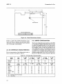
2-8. DC INTERFACE CHARACTERISTICS
The dc characteristics of the Multimodule board at
the J1 connector are listed in table 2-1.
2-9. JUMPER CONFIGURATION
The 22 user-configured jumper positions on the iSBX
311 Analog Input Multimodule Board allow the user
to select the operating mode for the input multiplexers and the DAC, and select the voltage gain for
the amplifier. Table 2-2 lists the functions of the
user-configurable jumpers. The Multimodule board
is configued to the single ended bipolar mode of
operation when shipped from the factory; this
includes jumpers from E5 to E6, E8 to E9, EIO to
E13, Ell to E12, E15 to E16, and E19 to E20. The
Table 2-1. DC Interface Characteristics
Type
Drive
IOl MAX
(mA)
VOL MAX
(IOL = MAX)
10H MAX
(PA)
VOH MIN
(loH = MAX)
Co MIN
(pf)
TRI
TTL
2.0
1.6
0.5
0.5
-200
-100
2.4
2.4
130
40
Type
Receiver
III MAX·
(Vll = 0.4)
Vil MAX
IiH MAX
(VIH = 2.4)
VIH MIN
CI MAX
(pF)
MOO-MD7
TRI
MAO
MCSOI
TTL
TTL
MRESET
IOWRT/, IORDI
MCLK
TTL
TTL
TTL
-0.5
-0.5
-4.0
-2.1
-1.0
-2.0
0.8
0.8
0.8
0.8
0.8
0.8
Output
Signal
MOD-M07
MINTRO
Input
Signal
TTL = Standard Totem Pole Output
TRI = Three-State
2-2
60
60
100
100
100
100
2.0
2.0
2.0
2.0
2.0
100
40
40
40
40
40
40
Preparation for Use
iSBX 311
IC
.400
SOCKET
-i-----T--
I
~
MULTIMODULE" BOARD
&.....--~---r------,.-r-------rr----
1.127
.337
.500
L
iSBX'· BUS
CONNECTOR
(MALE)
IC
f----------I
SOCKET
iSBX'· BUS
CONNECTOR
(FEMALE)
067
)
MICROCOMPUTER BOARD
~
~Ao.----~----.-r----~.093
Figure 2-2. Mounting Clearances (Inches)
following paragraphs give more details on the
various other jumper configurations available to the
user.
INPUT MULTIPLEXER MODE SELECTION.
Jumpers E19, E20, and E21 configure the multiplexer enable logic for either single-ended (connect
El9 to E20) or differential (E20 to E21) operation.
Single ended operation allows only one of the input
multiplexers to be enabled; differential operation
requires that both multiplexers be enabled to input
both halves of the differential signal.
INPUT MULTIPLEXER CONFIGURATION.
Jumpers E8, E9, Ell, and El2 configure the Multimodule board for either single ended (connect EB-to
E9 and Ell to E12) operation or differential (E9 to
E12) operation. The jumper connections control
which of the multiplexer outputs become amplifier
inputs. For pseudo-differential mode operation,
connect jumpers E8 to E9 and El2 to, E13; this
allows the ground reference to float with the user
input signal.
DAC MODE SELECfION. The operating mode of
the A-to-D converter is jumper selectable via
jumpers E14, E15, El6 and El7 to either Unipolar (0
to 5 volts) input mode or Bipolar (-5 to +5 volts) input
mode.
Unipolar operation (0 to 5 volts) requires a jumper
from El4 to El5 and El6 to El7 to connect two
internal DAC resistors in parallel into the signal
path. ,
Bipolar operation (-5 to +5 volts) requires a jumper
from El5 to E16. This configuration connects only
one internal DAC resistor into the signal path and
allows the DAC to be offset by 1.0 rnA (half scale).
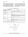
VOLTAGE GAIN: SELECfION. As shipped from
the factory, the Multimodule board contains a
2-3
Preparation for Use
iSBX 311
jumper connecting E5 to E6 and no resistors from
E3 to E4 and E 1 to E2. This configures the board for
a gain of 1. Configuration for a gain other than 1 is
performed by removing the jumper co.nnecting E5 to
E6 and installing resistors at the mounting locations E1 to E2 (Rb) and E3 to E4 (Ra). Refer to table
2-3 for a list of resistor values and the voltage gains
that they produce. The resistors shown in figure 2-3
must be axial 0.4 inch lead spacing to fit into the
moun ting positions (Ra is beneath U3, Rb is
between U2 and U3). The capacitor (Cb in figure 2-3)
must have 0.3 inch lead space in order to fit properly
into the mounting position (E5 to E7) under the U3
socket on the board.
Table 2-2. User-Configured Jumpers
Jumper Functions
Jumper Position
Number
Comments
Mode Selection for
Input Multiplexers
E19, E20, E21
Connect E19 to E20*-single ended operation, 16 channels maximum. Connect
E20 to E21-differential operation, 8 channels maximum.
Mode Selection for
Input Multiplexers
E8, E9, E11, E12
Connect E8 to E9* and E11 to E12*-single ended. Connect E9to E12-differential
operation.
Analog Ground onto
Input Returns
E10, E12, E13
Connect E10 to E13* to provide an analog ground out to the odd numbered pins
of the J1 connectors.
Connect E12 to E13 for pseudo-differential operation; the signal grounds float
with respect to the board ground thereby eliminating ground loops. However,
the ground differential must not exceed ±10V.
Mode Selection for
DAC
E14, E15, E16, E17
Connect E14 to E15 and E16 to E17 -unipolar operation. Connect E9 to E1O:
bipolar operation.
Voltage Gain Select
for Amplifier
E5, E6, E7
Connect E5 to E6*-Gain of one. Connect E5 to E7-mounting location for usersupplied capacitor to control noise.
Install resistors into mounting locations for user-configuration of voltage gain;
see table 2-3.
E1-E2, E3-E4
NOTES: * indicates the as-shipped configuration of the jumpers.
LF354
vIN-----------~
Ra
Rb
E1
">-----tlt-----'~VOUT
E2
E3
E4
Cb
E7
E5
I
I
I
I
I
------1
E6
Figure 2-3. Voltage Gain Resistor Location
2-4
iSBX 311
Preparation for Use
For higher gain applications, Rb should be 200
ohms or less to minimize noise pickup. Some configuration examples are listed in table 2-3.
Table 2-3. Gain Resistor Values
GAIN
Ra VALUE
Rb VALUE
none
2.5K
6K
4K
3.5K
4.5K
19K
none
2.5K
2K
1K
500 ohms
500 ohms
100 ohms
**
**
50 ohms
50 ohms
1
2
4
5·
8
10
20
50
250*
NOTE
When selecting an Rb resistor value, bear in
mind that the smallest possible value of Rb
will provide the best possible noise immunity.
When installing resistors Ra and Rb,
and capacitor Cb, ensure that the U3
and U4 chip sockets and surrounding
traces are not contaminated with solder. Failure to do so could result in
damage to the board.
Notes: * suggested maximum gain configuration.
** choose Ra so that Rb does not exceed 50
ohms.
To choose the proper resistor values (Ra and Rb) for
your application, first decide how much gain is
required for the application and then calculate the
resistor values as follows:
The Multimodule board includes a mounting position for the user-installed capacitor (Cb in figure 2-3)
under the U4 socket. The capacitor operates with Ra
to increase the noise immunity of the board at the
expense of reducing the bandwidth.
.
V OUT
Voltage Galn = - V
IN
Capacitor Cb provides the user the ability to dampen
high frequency noise at the U3 amplifier for applications using a higher gain. The capacitor works with
Ra to form a time constant of approximately 1mS
duration to allow time for the amplifier output to
settle. The value of the capacitor is dependent on the
value of resistor Ra, as shown in the following
equation:
Consider these examples. If a voltage gain of 2 is
required, then· the resistors Ra and Rb must be
chosen such that Ra =Rb. For a voltage gain of 10,
Ra and Rb must be chosen such that Ra = 9Rb. Each
. case, however, requires that the total resistance (Ra
+ Rb) can be approximately 2000 ohms so that the
amplifier can supply the required current output.
Table 2-4. iSBXTM BUS Pin Assignment
PIN
35
33
31
29
27
25
23
21
19
17
15
13
11
MNEMONIC
GND
MDO
MD1
MD2
MD3
MD4
MD5
MD6
MD7
GND
10RDI
10WRTI
MAO
9
7
5
3
1
. RESET
GND
+12V
DESCRIPTION
PIN
SIGNAL GROUND
M DATA BIT 0
M DATA BIT 1
36
34
32
M DATA BIT 2
M DATA BIT 3
M DATA BIT 4
M DATA BIT 5
M DATA BIT 6
M DATA BIT 7
SIGNAL GROUND
10 READ COMMAND
10 WRITE COMMAND
30
28
26
24
22
20
18
16
14
M ADDRESS 0
Reserved
Reserved
RESET
SIGNAL GROUND
+12V
12
10
8
6
4
2
DESCRIPTION
MNEMONIC
+5V
+5V
Reserved
Reserved
Reserved
Reserved
Reserved
Reserved
MCSOI
+5V
MINTRO
MPRT
MCLK
+5V
-12V
M CHIP SELECT 0
Reserved
+5V
Reserved
M INTERRUPT 0
Reserved
Reserved
M PRESENT
M CLOCK
+5V
-12V
2-5
Preparation for Use
iSBX 311
8(Ra)( Cb) = 1 mS delay, therefore,
2-11.
.
1 mS delay
CapacItance (Cb) = 8(Ra)
The Multimodule board may be configured to
operate in one of four modes; single-ended with
unipolar analog to digital (A-to-D) circuitry operation, single-ended with bipolar A-to-D circuitry
operation, differential with unipolar A-to-D circuitry
operation, and differential with bipolar A-D circuitry operation. Figure 2-4 shows a typical configuration for the Multimodule board in a single ended
input application and figure 2-5 shows a typical
differential input application.
Where Ra is listed in terms of ohms and Cb in terms
of farads.
NOTE
When changing channels with a Cb capacitor installed onto the Multimodule board,
the first conversion should be ignored and a
second con version of the same channel
should be performed 1 millisecond later to
obtain correct data.
Signal Ground Isolation. The signal ground may
be isolated from the Multimodule board ground by
removing the jumper connecting EI0 to E13 and
installing one from E12 to E13. This procedure
eliminates a potential ground loop problem by
connecting the analog signal ground directly to the
input of the amplifier.
.
Ensure that the potential on your analog
signal ground does not exceed ±12 volts.
Failure to do so could result in damage to
the amplifiers on the board.
2-10.
CONNECTOR CONFIGURATION
The Multimodule board contains two connectors,
the iSBX bus connector (PI) and the 1/0 connector
(Jl). Each of these is described in the following
paragraphs.
The iSBX bus connector (PI) interfaces the Multimodule board to any host iSBC microcomputer that
contains an iSBX bus connector. The signals found
on each pin of connector PI are listed in table 2-4
and described in Chapter 4.
The input connector (Jl) interfaces the Multim6dule
board to the application via user-supplied analog
data lines (channels). The channel input found on
each pin of connector Jl is listed in table 2-5. As the
table shows, the Multimodule board provides all but
four signals that are present on the J2 connector of
the iSBC 711 and 732 boards; the non-supported
signals include Clock Out, External Trigger In, EOC
Status Out, and EOS Status Out on pins 40, 42, 44,
and 46 respectively. Table 2-6 contains a list of part
numbers for compatible user-supplied connectors to
interface to the 50-pin Jl connector on the Multimodule board.
2-6
BOARD CONFIGURATION
Figure 2-4 shows the input stages to the Multimodule board when configured for the single-ended
operation. The single ended analog channel inputs
may be used with the A-to-D circuitry operating in
either the unipolar or bipolar mode. The only
hardware difference between the single ended
bipolar and single ended unipolar A-to-D circuitry
operation is that the A-to-D converter configuration
changes.
The input stages for the Multimodule board configured for differential operation are shown in figure 25. In this configuration, the differential analog
channel inputs may be used wA-to-D circuitry
operating in either the unipolar or bipolar mode.
2-12.
BOARD INSTALLATION
The Multimodule board mounts directly onto a host
iSBC microcomputer. Figure 2-6 shows the assembly
of the boards u mounting screws and spacer. Install
the board as follows:
With a plastic screw, 1/4 by 6-32, secure the
plastic 112 by 6-32 spacer to the host iSBC
board.
b. Locate pin 1 of the iSBX bus connector (PI) on
the Multimodule board and align it with pin 1 of
the iSBX bus connector on the host iSBC
microcomputer.
c. Align the mounting hole on the Multimodule
board with the mounting spacer installed onto
the host iSBC board in the first step.
d. Gently press the two boards together until the
connector seats.
e. Secure the Multimodule board to the top of the
spacer with another plastic 114 by 6-32 screw.
a.
NOTE
The location of an installed Multimodule
board and the iSBX bus connector number
on the host iSBC microcomputer may vary
according to the type of host iSBC microcomputer that is used.
iSBX 311'
Preparation. for Use
Table 2-5. Connector JI Pin Assignment
SINGLE-ENDED
PIN
1
Not Used
3
Analog Return
Analog Return
Analog Return
5
7
9
11
13
15
17
19
21
DIFFERENTIAL
Not Used
Analog Return
Analog Return
Analog Return
PIN
2
4
6
Analog
Analog
. Analog
Analog
Analog
Analog
Analog
Return
Return
Return
Return
Return
Return
Return
Analog
Analog
Analog
Analog
Analog
Analog
Analog
Return
Return
Return
Return
Return
Return
Return
8
10
12
14
16
18
20
22
Analog
Analog
Analog
Analog
Analog
Analog
Return
Return
Return
Return
Return
Return
Analog
Analog
Analog
Analog
Analog
Analog
Return
Return
Return
Return
Return
Return
24
26
28
30
32
34
Not Used
Not Used
Not Used
Not Used
Not Used
Not Used
Analog Return
-12v
36
38
40
23
25
27
29
31
33
35
37
39
41
Not Used
43
45
47
49
Not Used
Not Used
Analog Return
-12v
Not Used
Not Used
Not Used
42
44
46
48
50
SINGLE-ENDED
DIFFERENTIAL
Not Used
Channel 0
Not Used
Channel 0 High
Channel 8
Channel 1
Channel 0 Low
Channel 1 High
Channel
Channel
Channel
Channel
Channel
Channel
Channel
Channel
Channel
Channel
Channel
Channel
Channel
Channel
Channel
Channel
Channel
Channel
9
2
10
3
11
Channel 4
Channel 12
ChannelS
Channel 13
Channel 6
Channel 14
Channel 7
Channel 15
Not Used
Not Used
*Not Used
*Not Used
*Not Used
*Not Used
Analog Return
+12v
1
2
2
3
3
4
4
5
5
6
6
7
7
Low
High
Low
High
Low
High
Low
High
Low
High
Low
High
Low
Not Used
Not Used
*Not Used
*Not Used
*Not Used
*Not Used
Analog Return
+12v
Note: All odd-numbered pins (1, 3, ... 49) are on component side of the board. Pin 1 is the right-most pin when viewed from
the component side with the board extractors at the top.
An * marks those pins that are available on the iSBC 711 and 732 board interface, but not available on the Multimodule
board interface.
Table 2-6. Compatible JI Connector Details
Function
No. Of
Pairs
Pins
Centers
(Inches)
Connector
Type
Vendor
Vendor Part No.
3M
3M
AMP
ANSLEY
SAE
3415-0000* WITH EARS
3415-0001 W/O EARS
88083-1
609-5015
S06750 SERIES
Parallel
I/O
Connector
25/50
0.1
Female
Flat Crimp
Parallel *
I/O
Connector
25/50
0.1
Female
Soldered
GTE
VIKING
MASTERITE
Parallel
I/O
Connector
25/50
0.1
Female'
Wirewrap
TI
VIKING
ITT CANNON
6A001-25-1A 1-00
3KH25/9JN5
N008GR25-0R-H-X
H421011-25
3KH25/JN05
EC4A050A1A
Notes: * indicates that the connector includes screw-hold flanges that may have to be removed before installation.
2-7
Preparation for Use
iSBX 311
ANALOG INPUT
BUFFER
AMP
CHANNEL 0
ANALOG
INPUT
MULTIPLEXER
U6
CHANNEL 7
SEL
CHANNEL
SELECTOR
DECODE
U11
DIFFERENTIAL
AMP
E20
EB
CHANNEL B
OE12
BU:J~
R
ANALOG
INPUT
MULTIPLEXER
US
I
I
I
I
CHANNEL F
E13
SIGNAL GROUND
Figure 2-4. Single Ended Input Configuration
CHANNELO
CHANNEL 7
BUFFER
AMP
HI
ANALOG
INPUT
MULTIPLEXER
U6
HI
SEL
CHANNEL
SELECTOR
DECODE
U11
DIFFERENTIAL
AMP
E20
CHANNEL 0
LOW
ANALOG
I
MU~~I~~~XER
I
I
CHANNEL 7-
E9
US
I
LOW
E13
)
SIG"NAL GROUND
E10
J~
BOARD GROUND
Figure 2-5. Differential Input Configuration
2-8
iSBX 311
Preparation for Use
MULTIMODULE BOARD
1/2" THREADED PLASTIC SPACER
MICROCOMPUTER BOARD
1/4" 6-32 PLASTIC SCREW
Figure 2-6. Mounting Technique
2-9/2-10
CHAPTER 3
PROGRAMMING INFORMATION
3-1.
INTRODUCTION
the A register before the OUT instruction is directed
to one of the legal WRITE port addresses for the
Multimodule board (see table 3-1). The format of the
channel selection byte is shown in figure 3-1. The
channel selection byte (bits CO, C1, C2, and C3) is
decoded by the Multimodule board to select one of
the 16 (for single ended operation) or one of 8 (for
differential operation) analog input channels. The
high order bits (X, X, X, X) are not used. The WRITE
command is issued via an OUT instruction. When
the OUT command is executed by the host iSBC
microcomputer, the accumulator must contain the
proper channel address, as listed in table 3-2.
This chapter describes the user programming
required for the iSBX 311 Analog Input Multimodule
Board. Included are sections on addressing, command formats, data selection formats, interrupt
servicing, and programming examples.
3-2. ADDRESSING
The Multimodule board is addressed by executing
an IN or OUT instruction in the host iSBC microcomputer to one of the legal port addresses for the
Multimodule board. Since some host iSBC microcomputers will accept up to three Multimodule
boards, the upper address byte for each iSBX bus
connector will vary, as table 3-1 shows. The port
addresses vary according to whether an 8-bit board
or a 16-bit board is used as the host iSBC microcomputer board.
3-3. COMMAND FORMAT
The Multimodule board is capable of responding to 2
types of commands, READ commands and WRITE
commands. The READ command causes digital
data (high byte, low byte, or status) to be transferred
to the host iSBC microcomputer and the WRITE
command transfers the channel address to the
Multimodule board to select which channel will be
converted. Each of the commands is issued by the
host iSBC microcomputer via either an IN or an
OUT instruction directed to one of the legal port·
addresses.
The WRITE command must select the channel on
the Multimodule board which is to be converted; this
consists of loading the channel selection byte into
When a READ command (IN instruction) is directed
to one of the legal Multimodule port addresses and is
decoded by the Multimodule board, the command
causes converted digital data to be sent to the host
iSBC microcomputer from the Multimodule board·
data buffers. The READ command may call for
either the status of the Multimodule board, the LOW
BYTE of converted data, or the HIGH BYTE of
converted data. The data, recall, is the result of an
analog data conversion sequence from the channel
selected by the previous WRITE command. The
distinction between the LOW and HIGH data bytes
is performed by the port address used; refer to table
3-1.
NOTE
The RESET occurring as a result of poweron will not clear the interrupt request signal
(INTRa) from the Multimodule board.
Therefore, a READ HIGH BYTE command
should be issued after power-up to clear the
INTRa signal before starting an operation.
Table 3-1. 1/0 Port Addresses
FUNCTION
a-BIT PORT ADDRESS
16-BIT PORT ADDRESS
COMMENTS
READ HIGH BYTE
XO, X2, X4, or X6
XO, X4, XB, or XC
Transfer converted data from Multimodule board and resets the interrupt
request line.
READ LOW BYTE
and READ STATUS
X1, X3, X5, or X7
X2, X6, XA, or XE
Transfer converted data and status from
Multimodule board.
WRITE CHANNEL
SELECT ADDRESS
XO through X7
XO through XE
WRITE next channel address to Multi·module board and initiate conversion.
Note: Refer to the Hardware Reference Manual for your host iSBC microcomputer to determine the upper digit (X) of the
Multimodule port address.
3-1
Programming Information
bit position
7
6
iSBX 311
5
4
3
2
0
I
Channel Select Byte r-1X- r -X---.-I-X---.-I-X--r-I-C-3.....I-C-2..,.I-C-1..,.'-C-0.....
Figure 3-1. Channel Selection Byte Format
bit position
LOW BYTE
7
6
5
4
3
2
1
0
I
03' 02101 'DO' 0 'START/ , BUSy/I EOC/
HIGH BYTEID111D10lD91081D71
D6
D5
D4
Figure 3-2. Data Format
3-4. DATA FORMAT
3-5. STATUS FORMAT·
A READ command is issued to the multimodule
board to initiate a READ operation in which
converted data is sampled by the host iSBC microcomputer. The digital data created within the
Multimodule board is the result of operation of the
SAR, the DAC, and the comparator to transform the
analog input data into 12 bits of digital data which
are left-justified through two three-state multiplexers to form two 8-bit bytes of digital data. The
format of the digital data bytes created by the
Multimodule board is shown in figure 3-2. Bits DO
through D3 of the low byte interface to bidirectional
bus lines MD4 through MD7, respectively. The low
byte includes one unused bit (bit 3) and the status
bits (EOC/, BUSY I, and START I on MDO, MD1,
and MD2, respectively). The high byte includes data
bits D4 through Dll which are transferred on
bidirectional bus lines MDO through MD7, respectively.
Status for the Multimodule board is contained in the
three least significant bits of the LOW BYTE of data
(see figure 3-2). The status is read by the host iSBC
microcomputer whenever a READ LOW BYTE
command is issued by the host iSBC microcomputer
to the Multimodule board. When a READ LOW
BYTE command is issued, the status bits are
released onto the MDO, MDl, and MD2 data lines.
The STARTI status bit (bit 2) is used by the host
iSBC microcomputer to determine whether or not
the A-to-D converter on the Multimodule board has
started data conversion. When the STARTI bit is
LOW, it indicates that the Multimodule board is in
the process of sampling the analog data input; i.e.,
the A-to-D conversion is begun. When the STARTI
bit is HIGH, it indicates that the data sampling is
completed.
Table 3-2. WRITE Commands
COMMAND*
CHANNEL**
SELECTION BYTE
OUT
OUT
OUT
OUT
OUT
OUT
XX
XX
XX
XX
XX
XX
00
01
02
03
04
05
OUT
OUT
OUT
OUT
OUT
OUT
OUT
OUT
XX
XX
XX
XX
XX
XX
XX
XX
06
07
08
09
OA
OB
OC
OD
OUT XX
OUT XX
OE
OF
Notes:
MODE
FUNCTION
Single
Single
Single
Single
Ended/Differential
Ended/Differential
Ended/Differential
Ended/Differential
Select
Select
Select
Select
channel
channel
channel
channel
00
01
02
03
input.
input.
input.
input.
Single
Single
Single
Single
Single
Single
Single
Single
Single
Single
Single
Ended/Differential
Ended/Differential
Ended/Differential
Ended/Differential
Ended
Ended
Ended
Ended
Ended
Ended
Ended
Select
Select
Select
Select
Select
Select
Select
Select
Select
Select
Select
Select
channel
channel
channel
channel
channel
channel
channel
channel
channel
channel
channel
channel
04
05
06
07
08
09
10
11
12
13
14
15
input.
input.
input.
input.
input.
input.
input.
input.
input.
input.
input.
input.
Single Ended
* XX is any legal WRITE port address, as defined in table 3-1. Refer to the respective Hardware Reference Manual
for the host iSBC microcomputer for port addresses.
** The Channel Selection Byte must be contained in the accumulator in the CPU on the host iSBC microcomputer
board.
3-2
Programming Information
iSBX 311
The BUSY1 status bit (bit 1) is generated by the
SAR to show the condition of the successive
approximation routine that occurs for each data
input sequence on the Multimodule board. When the
dat conversion is started, the BUSY 1 signal goes
LOW a maximum of 3.8 microseconds after START1
goes LOW. When the board is finished converting·
the analog data to digital data, BUSY 1 goes HIGH,
indicating that the conversion within the SAR is
fully completed; i.e., data is available in the form of
a HIGH BYTE and LOW BYTE.
The EOCI status bit (bit 0) is used by the host iSBC
microcomputer to determine the end of conversion
when the host must determine the status of the
Multimodule board by polling the status byte. The
EOCI status bit is reset by issuing a READ HIGH
BYTE command to the Multimodule board. The
interrupt line (INTRO) from the Multimodule board
is an inverted version of the EOCI signal and is also
reset on a READ HIGH BYTE command. The
interrupt line may be used to request an interrupt
from the host iSBC microcomputer at the end of a
conversion.
3-6. PROGRAMMING EXAMPLE
Table 3-3 contains a programming example for the
Multimodule board that will read data from each of
sixteen single-ended analog input channels and
store the converted data in a 32-byte table in
memory. A program for a differential system would
be similar, with the exception that only 8 channel
inputs are available. The example uses a data table
to store up to 32 bytes of converted analog data
input through the Multimodule board. All 16
channels are scanned, implying that the Multimodule board is configured to operate in the single
ended mode. The end of a conversion cycle is sensed
by polling for the EOCI signal transition. The port
addresses used in the sample program are for use
with an iSBC 80/24 board (J6 Multimodule board
connector) and may have to be altered if another
host or another Multimodule connector is required.
For proper port addresses, refer to table 3-1 of this
manual.
Table 3-3. Programming Example
TABLE:
HIGH
OS
EQU
32
OFOH
LOW
EQU
OF1H
ADR
EQU
OFOH
ALL 16:
LXI
H,TABLE + 31
MVI
B,15
IN
HIGH
MOV
A,B
OUT
ADR
IN
LOW
;READ status byte to
;check for end of
;conversion.
ANI
01H
JNZ
INTR
IN
LOW
ANI
HIGH
;Checking for EOC/
;bit.
;Waiting for end of
:conversion.
;READ LOW BYTE of
;data.
;Mask off non-data
;bits of low byte.
MOV
M,A
DCX
H
IN
HIGH
MOV
M,A
OCR
B
;Store high byte data
;into table.
;Decrement channel
;counter.
;Return when all 16
;channels serviced.
LOOP
;Go to next channel.
LOOP
INTR
RM
JMP
END
;Define data table.
;High byte port
;address.
;Low byte port
;address.
;Channel select port
;address.
;Set data-table
;pointer.
;Set-up channel
;counter.
;Ensure EOC/ bit
;RESET
;(READ HIGH BYTE)
;Move next-channel
;address to A.
;WRITE channel
;address to Mtuli;module board and
;start conversion on
;channel data.
;Store low byte data
;into table:
;Decrement memory
;pointer.
;READ HIGH BYTE
;of data from the
;Multimodule board.
3-3/3-4
CHAPTER 4
PRINCIPLES OF OPERATION
4-1. "INTRODUCTION
This chapter provides a functional description of the "
interface signals detailing the circuit operation for
the iSBX 311 Analog Input Multimodule Board. The
functional description of the board includes details
on the operation of each of the major components on
the board, as shown in the functional block diagram
in figure 4-1.
4-2. iSBX™ BUS INTERFACE SIGNAL
DESCRIPTION
The Multimodule board is controlled by the signals
on the iSBX bus connector. The iSBX bus signals
and their functions are detailed in the following
paragraphs.
RESET (Reset)-This active high signal, when
asserted to the Multimodule board, clears the clock
divider and interrupt request circuitry on the board.
The DAC, Sample-and-Hold, and SAR devices are
not directly affected by RESET.
MCLK (Clock)-This signal is derived from the host
iSBC microcomputer to provide synchronous operation. MCLK is a 9 to 10 MHz clock provided by the
host iSBC microcomputer. It is used by the Multimodule board to generate a 2.7 to 2.5 microsecond
clock for the on-board Successive Approximation
Register (SAR).
MDO-MD7 (Bidirectional data bus)-These eight
bidirectional data lines provide a means of transferring commands and data to or form the Multimodule board. When not in use, the MDO-MD7 lines
are held at high impedance. When both MCSOI and
IORDI (or MCSOI and IOWRT I) are LOW, the data
lines are enabled.
IORDI (Read Command)-This active low signal is
generated by the host iSBC microcomputer as a
command to the Multimodule board to input data to
the host. IORDI works with MCSOI and MAO to
enable the bidirectional data bus (MDO-MD7) for
input, to reset the clock divider/interrupt request
circuitry, and to select whether the low or high data
byte is to be sent to the host.
MCSOI, the IOWRT I signal causes the channel
selection circuitry to be loaded with the address of
the channel from which input is desired, and causes
the data conversion process to begin.
MCSOI (Select)-MCSOI is an active low input
signal to the Multimodule board to allow it to accept
either an IORDI or IOWRTI command from the
host iSBC microcomputer board. When HIGH,
MCSOI holds the bidirectional data bus in a high
impedance state.
MAO (Byte Selector)-This input from the host
iSBC microcomputer is used during a READ operation to select whether the data put on the bidirectional bus by the Multimodule board is to be the
high or low byte of the last conversion. When MAO
is LOW (along with MCSOI and IORD/), the
Multimodule board gates the HIGH BYTE (data bits
Dll, DI0, D9, D8, D7, D6, D5, and D4) onto MD7MDO (respectively) to the host. When MAO is HIGH,
the Multimodule board gates the LOW BYTE (data
bits D3, D2, Dl, DO, 0, START/, BUSY/, and
INTRO/) onto MD7-MDO (respectively); 0 indicates
that the bit position is not used and may be ignored.
INTRO (Interrupt O)-This active high output signal
provides an indication to the host iSBC microcomputer that the analog data conversion for the last
channel is completed (BUSY ImO) and that service
from the host iSBC microcomputer is required. The
falling edge of BUSYI advances the count in the
binary counter (U8), changing the output from pin-3
to a HIGH. This output is the interrupt request
signal (INTRO) from the Multimodule board and
may be cleared by either a RESET pulse to U14 pin12 or by performing a READ HIGH BYTE command decode from U14 pin-3 which is inverted to
reset U8.
4-3.
FUNCTIONAL DESCRIPTION
The functional description is based upon the
functional block diagram shown in figure 4-1. Each
functional block in the figure is explained in detail
in the following paragraphs.
4-4. INPUT CHANNEL SELECTOR
IOWRTI (Write Command)-This active low signal
is generated by the host iSBC microcomputer as a
command to the Multimodule board to accept data
present on the bidirectional data bus. Along with
Logic device Ull serves as a decoding device to
determine which input chjannel to the Multimodule
board is selected for output to the host iSBC
4-1
iSBX 311
Principles of Operation
microcomputer. The channel selection byte (refer to
figure 3-1) from the host is decoded into MPXA,
MPXB, MPXC, MPXl, and MPX2 signals to operate
the channel selector devices (U5 and U6). These
signals select one of 8 differential or one of 16 singleended analog input channels.
4-5. CHANNEL MULTIPLEXERS
The channel multiplexers (U5 and U6) receive the
analog inputs from an external source. As shipped
from the factory, the analog multiplexers are set up
to operate in the single ended mode. In single ended
mode operation, only one multiplexer is enabled on
any operation to select channel data input; one of
sixteen channel inputs. In differential mode operation, the Multimodule board allows both U5 and U6
to operate simultaneously in multiplexing both
halves of a differential channel input signal;
selection of one of eight channel inputs. As a safety
feature, the multiplexers contain an internal device
to protect against overvoltage surges of up to 30
volts.
4-6. OUTPUT DATA BUFFERS
The output data buffers (U12 and U13) provide an 8bit register in which converted data for the host
iSBC microcomputer can be held until requested.
Depending on the command of the host, the buffers
can pass either the HIGH BYTE or the LOW BYTE
of the last data conversion to the host via the
bidirectional bus. The buffers are held in a high
impedance condition when not in use. The data in
the register may be read as many times as desired,
Ihowever, after reading the HIGH BYTE, the EOCI
status bit (bit 0) is reset and should be considered
not valid until after the next data conversion
sequence.
multiplexers (data bits D4, D5, D6, D7, D8, D9, DlO,
and Dll) are connected to the MDO through MD7
data lines, respectively.
4-7. SAMPLE-START PULSE GENERATOR
The monostable multi vibrator (U9) is triggered at
the end of the period when IOWRTI and MCSOI are
LOW. The mutivibrator generates a 10 to 15 microsecond Sample-and-Hold (SH)pulse to sample the
analog data into the Sample-and-Hold circuitry (U7)
and also generates a Start-Conversion pulse
(START/) to trigger the SAR to start a data
conversion sequence.
4-8. BUFFER AMPLIFIERS
The two buffer amplifiers (both contained in U4)
provide high impedance for the input multiplexers
(U5 and U6) and for the signal source to prevent
unnecessary input line lading. The buffer amplifiers
also provide a low input impedance for the differential amplifier (U3).
4-9. DIFFERENTIAL AMPLIFIERS
The differential amplifier (U3) operates as a unitygain bipolar amplifier. The amplifier provides a
single-ended output that is the difference between
the outputs on pin-l and pin-7 from the buffer
amplifiers (U4). The output of the amplifier feeds the
gain select and offset adjust stage of U3. The
amplifier includes four 0.02 percent resistors (R8,
R9, Rll, and R12) to provide greater than 60 db
Common Mode Rejection (CMR). Capacitors Cll
and C12 are included to filter high frequency noise
from the data.
To pass the LOW BYTE of converted data (bits D3,
D2, Dl, and DO on MD7 through MD4) and the
status bits (on MD3 through MDO), the Multimodule
board must sense a LOW on the IORDI line, a LOW
on MCSOI, and a HIGH on MAO. These signals
enable the output buffers (U12 and U13) to operate
and the MAO signal also provides the output
sequencing control for the output buffers. The MAO
signal is initially HIGH to select the "B" inputs to
the U12 and U13 multiplexers; i.e., EOCI, BUSY I,
START/, zero, DO, Dl, D2, and D3 are output on
data lines MDO through MD7, respectively, to the
host iSBC microcomputer.
4-10. AMPLIFIER GAIN SELECT. The gain
select is user configurable through jumper/resistor
locations (El through E7); factory configuration
includes a jumper from E5 to E6 which configures
the board to a gain of one. The Multimodule board
may be configured for a maximum gain of 250 by
installing two resistors (Rb from El to E2 and Ra
from E3 to E4) and removing the jumper from E5 to
E6. Configuration also includes installation of filter
capacitor Cb from E5 to E7 to limit the bandwidth.
More jumper wiring information is contained in
Chapter 2.
To pass the HIGH BYTE of converted data (bits D4,
D5, D6, D7, D8, D9, DlO, and Dll on MD7 through
MDO), the Multimodule board must sense a LOW on
the IORDI line, a LOW on MCSO/, and a LOW on
MAO. When MAO goes LOW, the "A" inputs to the
4-11. AMPLIFIER OFFSET ADJUST. The
offset adjust resistor (R2) and resistor RIO are
responsible for controlling the offset (if any) induced
into the input by the two buffers, the differential
amp, and the gain select circuitry. Chapter 5 of the
4-2
iSBX 311
text includes an adjustment procedure for the offset
R2). Once the offset on the channel input is corrected, the channel input is ready to be passed on to
the sample-and-hold stage.
4-12. SAMPLE-AND-HOLD CIRCUITRY.·
The sample-and-hold device (U7) samples the input
signal on pin-3 for 15 microseconds and holds the
sample for the duration of the conversion cycle. By
sampling and holding the input, the' Multimodule
board freezes the input signal for the duration of the
analog to digital (A-to-D) conversion so that a more
accurate A-to-D conversion can be performed. When
the sample-and-hold device senses a HIGH on pin-B
(the SH signal from U9), it samples the input on pin3. Capacitor C9 stores the sample of the input signal
voltage during the conversion.
4-13. ANALOG-TO-DIGITAL CONVERSION
The A-to-D Converter (ADC) logic on the Multimodule board consists of circuits to perform several
distinct functions, including:
•
a reference voltage (pin-24 of UI),
•
•
a Digital-to-Analog Converter (UI),
a voltage comparator (UIO),
•
a Successive Approximation Register-SAR (U2),
•
•
•
a clock (UB),
a DAC offset circuit (RI and RI4), and
a Dac gain adjust circuit (R3, R5, R6, and R7).
Each of these is discussed in detail in the following
paragraphs.
A voltage reference circuit of 6.3 volts within the
DAC (pin-24' of UI) establishes the full-scale current
reference for the DAC. More information on the
DAC can be found in the data book and data sheets
for the DAC device.
The DAC voltage gain adjust circuitry (R3, R5, R6,
and R7) modifies the full-scale voltage reference
output from the DAC by a maximum of 0.5% in order
to accurately set the full-scale reading for the DAC.
Chapter 5 contains a procedure for adjusting the
DAC voltage gain (R3).
The DAC offset adjust circuitry (RI and RI4)
establishes a true zero reading for unipolar operation or a negative full-scale reading for bipolar
operation. Chapter 5 contains a procedure for
adjusting the DAC offset (RI).
Principles of Operation
The SAR is a 12-bit register that sequentially tests
each bit against the value in the sample and hold
register. The state of each bit of the final output is
successively determined by the operation of DAC,
the sample-and-hold register, and the comparator
circuits. The result of the operation of these ciruits
builds, bit by bit, a digital data word within the SAR
device. One cycle for the SAR consists of 12
successive data approximations, and each approximation determines the proper value for one data bit
position within the SAR, starting with the most
significant bit and ending with the least significant
bit. As soon as the state of the last bit within the
, SAR is determined, the EOC/ signal from pin-3 of
the SAR goes LOW, indicating that conversion is
completed.
The voltage comparator circuitry includes some
internal DAC circuitry, amplifier UIO, diodes CRI
and CR2, resistor RI3, and capacitor CIB. For each
bit of the conversion operation, the comparator
circuitry compares the value held in the Sampleand-Hold register with the conversion value contained in the DAC, and with the results of the
compare operations, builds a converted data word in
the SAR. IfUIO senses a positive current flow at pin3, then a LOW is generated from pin-7 and fed back
into the SAR on pin-II to turn ON that particular bit
of the conversion data word. Conversely, if UIO
senses a negative current flow, then a HIGH is
generated from pin-7 to turn OFF that bit of the
conversion data word. Diodes CRI and CR2 limit
the voltage swing at the comparator in order to
increase con version speed.
4-14. CLOCK DIVIDER CIRCUITRY.
The Multimodule board includes on-board clock
divider circuitry (UB) that uses the MCLK signal (9
to 10 MHz clock) from the iSBX bus connector.
Device UB divides the MCLK signal by 25 to create a
CLOCK signal with a nominal 2.7 to 2.5 microsecond period. CLOCK controls the successive approximation cycle within the SAR; the nominal conversion time for one SAR cycle (12 bit approximation), including sample and hold time, is 50 microseconds.
4-15. INTERRUPT GENERATION
CIRCUITRY.
When the end of conversion signal is output from
the SAR device, the falling edge advances the count
in UB, generating an output from pin-3 of UB which
requests an interrupt from the host iSBC microcomputer. The interrupt request from UB remains
active until cleared by reading the HIGH BYTE of
data or by receiving RESET (the reset signal from
the iSBX bus connector).
4-3
iSBX 311
Principles of Operation
4-16. RESET GENERATION CIRCUITRY.
A RESET operation on the Multimodule board
clears only the interrupt request line (INTRO) from
UB. The RESET operation is performed through
device UI4 and QI and may be generated for the
Multimodule board in one of two methods:
a.
4-4
If a RESET command is issued by the host iSBC
microcomputer, the command is sensed on the
Multimodule board as RESET via pin-5 of the
iSBX bus connector. The power-on reset will not
clear the interrupt request line.
b.
If a READ HIGH BYTE command is issued to
the Multimodule board to input the upper byte of
the data word, UI4 pin-3 generates a pulse
which is inverted by Q2 to reset UB, clearing the
interrupt request line (INTRO) from UB. The
READ HIGH BYTE command also clears the
interrupt request line during initialization.
iSBX 311
Principles of Operation
.
ANALOG CHANNEL INPUT
V
"
~E21
IOWRTI
MCSOI
MOO
MOl
MD2
M03
CHANNEL
SELECTOR
DECODE
Ull
BUFFER
AMP
U4
ANALOG
INPUT
MULTIPLEXER
U6
""
lJ..
::...
LOW BYTE
DO 01 02 03
DIFFERENTIAL
AMP
~E20
GAIN
EFFECT
ADJUST
U3
U3
f----
SAMPLE!
HOLD
REGISTER
U7
""SEL
ANALOG
INPUT
MULTIPLEXER
US
ANALOG CHANNEL INPUT
~E8
E'
y
E13
SIGNAL GROUND
I~
E12
IOWRTI
MCSO!
El0
l
MDG
OUTPUT
BUFFER
U13
~
-!.
SH
. >MCSOI
>IORO!
~17
Ed.
BUFFER
M07
"
HIGH BYTE
08 09 010
11
DAC
U1
~
~
........
12-BITS
U10
>MAO
SAMPLEI
START
CLOCK
GUARANTEE
U9
~
V
LOW BYTE
.--
MD4
~I
HIGH BYTE
04 05 06.07
OFFSET
ADJUST
M05
STAT_U~
"
....
J
~
OUTPUT
BUFFER
U12
M03
MD2
MOl
V
....
~
MOO
START!
BOARD
-:- GROUND
SAR
U2
CLOCK
MCLK
ToCI
CLOCK
DIVIDER
US
RESET
J..~
I
l2-BITS
INTERRUPT
REQUEST
U8
INTROI
...
t
Figure 4-1. iSBX 31FM Board Functional Block Diagram (Single-Ended - Unipolar Operation)
CHAPTER 5
SERVICE INFORMATION
5-1. INTRODUCTION
This chapter provides a list of replaceable parts,
service diagrams, adjustment procedures, and
service and repair assistance instructions for the
iSBX 311 Analog Input Multimodule Board.
5-2.
SERVICE AND REPAIR ASSISTANCE·
United States Customers can obtain service and
repair assistance by contacting the Intel Product
Service Hotline in Phoenix, Arizona. Customers
outside the United States should contact their sales
source (Intel Sales Offices or Authorized Distributor) for service information and repair assistance.
Before calling the Product Service Hotline, you
should have the following information available:
a.
b.
c.
d.
e.
f.
Date you received the product.
Complete part number of the product (including
dash number). On boards, this number is
usually silk-screened onto the board. On other
MCSD products, it is usually stamped on a
label.
Serial number of product. On boards, this
number is usually stamped on the board. On
other MCSD products, the serial number is
usually stamped on a label.
Shipping and billing addresses.
If your Intel product warranty has expired, you
must provide a purchase order number for
billing purposes.
If you have an extended warranty agreement,
be sure to advise the Hotline personnel of this
agreement.
. Use the following telephone numbers for contacting
the Intel Product Service Hotline:
which will help Intel provide you with fast, efficient
service. If you are returning the product because of
damage sustained during shipment or if the product
is out of warranty, a purchase order is required
before Intel can initiate the repair.
In preparing the product for shipment to the Repair
Center, use the original factory packing material, if
possible. If this material is not available, wrap the
product in a cushioning material such as Air Cap
TH-240, manufactured by the Sealed Air Corporation, Hawthorne, N.J. Then enclose in a heavy duty
corrugated shipping carton, and label "FRAGILE"
to ensure careful handling. Ship only to the address
specified by Product Service Hotline personnel.
5-3.
ADJUSTMENT PROCEDURE
The adjustments for the iSBX 311 Analog Input
Multimodule Board include facilities for userperformed offset and voltage gain adjustments. The .
procedures are outlined in the following paragraphs.
Each Multimodule board is adjusted at the factory,
however, the boards should be readjusted on installation, and whenever reconfiguration occurs.
5-4. TEST EQUIPMENT REQUIRED
The test equipment required to adjust the gain and
offset for the Multimodule board is as follows:
a.
Digital Voltmeter with a voltage range of 0 to 15
volts and accuracy of ±0.005% or better.
b.
Precision voltage source; 0 to 15 volts dc
±0.001 (1\), continuously adjustable; source impedance less than 1.0 ohm.
All U.S. locations, except Alaska, Arizona &
Hawaii: (800) 528-0595
All other locations: (602) 869-4600
5-5. PRELIMINARY PROCEDURE
TWX Number: (910) 951-1330
Before beginning the calibration procedure, install
the Multimodule board onto a host iSBC microcomputer and verify the voltage levels of the dc
supply voltages as per table 5-1. If any of the voltage
levels are out of tolerance, they should be readjusted
before the calibration procedure is performed.
Always contact the Product Service Hotline before
returning a product to Intel for repair. You will be
given a repair authorization number, shipping
instructions, and other important information
5-1
iSBX 311
Service Information
'Table 5-1. Power Supply Voltage
Requirements
Supply
Tolerance
Voltmeter Connection
+12
-12
+ 5
±5%
±5%
115%
Across C23
Across C24
Across C21
a.
Connect the preCISIOn voltage source to the
connection points required for channel 0 as
listed in table 5-2.
Set the voltage source for the appropriate offset
input as required for the ADC range being used;
refer to table 5-3.
Call the ADCOFF subroutine and adjust the Rl
resistor until the readings on the monitor alternate equally between 000 and 001, as listed in
table 5-3.
b.
c.
Note: Refer to figure 5-1
for capacitor locations.
5-6. A-TO-D CONVERTER (ADC) CIRCUITRY CALIBRATION PROCEDURE. The calibration procedure for the A-to-D Converter (ADC)
circuits consists of a sequence of three steps which
must be performed in the following order: (1) amplifier offset adjustment, (2) ADC offset adjustment,
and (3) ADC range adjustment. These adjustments
, are explained in the following paragraphs. However, be aware that the procedures outlined in the
text assume that the calibration programs are run
on a microcomputer system that includes a monitor
screen and that contains a host microcomputer
board within the microcomputer system, and further
assumes that an ADC offset (ADCOFF) subroutine
and an ADC range (ADCRNG) subroutine are in the
resident program. Appendix A of this manual
includes an example of typical programs to use
when adjusting the ADC range and offset.
Table 5-2. ,ADC Offset and Range Adjustment
Test Input
Voltage
Input
High
Low
Ground
Source Connection
Single-ended
Differential
J2 pin 4
J2 pin 3
J2 pin 3
J2 pin 4
J2 pin 6
J2 pin 3
Table 5-3. Voltage Source Input Required
for ADC Offset and Range Adjustment
Operating
Mode
o to
+5 volts
±5 volts
Offset Adjust
Reading
Range Adjust
Reading
0.00061 volts
-4.9988 volts
4.9982 volts
4.9963 volts
NOTE
The calibration procedures are call for
adjusting the channel 0 input. Once channel
o is adjusted properly, it may be safely
assumed that the remaining channels are
adjusted properly.
5-9. ADC RANGE ADJUST PROCEDURE.
After the amplifier offset and ADC offset adjustments are made, adjust the ADC range as follows:
a.
b.
5-7. AMPLIFIER OFFSET ADJUST PROCEDURE. Adjust the amplifier offset as follows:
a.
Short input channel 0 by connecting J2 pin 4 to
J2 pin 3 (if in differential mode, also short J2 pin
6 to J2 pin 4).
b.
Set the DVM to the most sensitive dc voltage
scale. Then, connect the positive lead of the
DVM to E22 and the negative lead to jumper
post E18.
c.
Call the ADCOFF subroutine and adjust the R2
resistor to give a 0 volts reading on the DVM.
5-8. ADC OFFSET ADJUSTMENT PROCEDURE. After the amplifier is adjusted, adjust the
ADC offset as follows:
5-2
c.
Connect a precision voltage source to the
connection points for channel 0 input, as listed
in table 5-2.
Set the precision voltage source to the appropriate range input as required for the ADC
range being used; refer to table 5-3.
Call t he ADCRNG subroutine and adjust the
R3 resistor until the readings on the monitor
alternate equally between FFEH and FFFH, as
listed in table 5-3.
5-10.
REPLACEABLE PARTS
, Table 5-4 provides a list of replaceable parts for the
Multimodule board. Table 5-5 identifies and locates
the manufacturers specified in the MFR CODE
column of table 5-4. Intel parts that are available on
the open market are listed in the MFR CODE
column as "COML". Every effort should be made to
procure these parts from a local (commercial)
distributor.
iSBX 311
Service Information
Table 5-4. Replaceable Parts
Description
Reference Designator
Mfr. Code
Qty.
TI
TI
TI
TI
TI
TI
NAT
NAT
AOV
ANA
AOV
1
1
2
1
1
2
2
1
1
1
1
OBO
COML
1
OBO
OBO
OBO
OBO
OBO
COML
COML
COML
COML
COML
1
1
1
1
1
U9
U11
U12, U13
U14
U8
US, U6
U3, U4
U7
U2
U1
U10
IC,
IC,
IC,
IC,
IC,
IC,
IC,
IC,
IC,
IC,
IC,
R4
Resistor, 1.1K, %W, 5%
R7
R12
R13
R14
R15
Resistor,
Resistor,
Resistor,
Resistor,
Resistor,
R5, R6, R10
Resistor, 196K, YaW, 1%
OBO
COML
3
R8, R9, R11
Resistor, 2.5K, 1/20W, 0.02%, 10PPM
OBO
COML
3
R1, R2, R3
RP2
RP1
Resistor, 20K, V2W, 16 turn
Resistor Pack, 10K, 10 pin SIP, 9R
Resistor Pack, 1K, 6 pin SIP, 3R
3262X-203
4310R-101-103
4306R-1 02-1 02
BRN
BRN
BRN
3
1
1
C1
C8
C17
C18
C22
C25
Capacitor,
Capacitor,
Capacitor,
Capacitor,
Capacitor,
Capacitor,
aBO
aBO
aBO
aBO
aBO
aBO
COML
COML
COML
COML
COML
COML
1
1
1
1
1
1
C5, C7, C12, C13,
C16, C19, C20
Capacitor, dg., 0.1pF, 50V, +80%, -20%
aBO
COML
7
C10, C11, C14, C15
Capacitor, dg., 220pF, 50V, 10%
aBO
COML
4
C2, C3, C4, C6, C9
Capacitor, cer., 1pF, 50V, +80%, -20%
aBO
COML
5
C21
C23, C24
Capacitor, tant., 33pF, 10V, ±20%
Capacitor, tant., 15pF, 20V, ±20%
aBO
aBO
COML
COML
1
2
CR1, CR2
VR1
Q1
Diode HP2811
Diode, zener 1N4567
Transistor, PNP 2N4403
Shorting Plugs
Socket, SIP, 12-pin
Socket, SIP, 8-pin
Socket, SIP, 4-pin
Connector, 36-pin
Stake pins, brass
aBO
aBO
aBO
530153-2
7195-295-5
7195-295-5
7195-295-5
000292-0001
87623-1
COML
COML
COML
AMP
EMC
EMC
EMC
VIK
AMP
2
1
1
5
4
2
4
1
15
P1
E8-E22
Monostable Multivibrator
Quad O-type Flip-Flop
Quad 2-to-1 Multiplexer
Quad 2-input OR
Dual 4-bit Counter
8-to-1 Analog Multiplexer
Dual Op. Amplifier
Sample and Hold Register
Successive Approx. Register
Digital To Analog Converter
Comparator
Mfr. Part No.
39.2K, YaW, 1%
2.5323K, 1/20W, 0.02%, 10PPM
3.9K, YaW, 5%
681K, YaW, 1%
150 ohm, %W, 5%
cer., 0.01pF, 50V, +80%, -20%
cer., 0.001pF, 50V, 10%
cer., 1800pF, 50V, 10%
cer., 33pF, 50V, 5%
cer., 0.1pF, 50V, +80%, -20%
dg., 0.01pF,.50V, +80%, -20%
74121
74175
74LS258A
74LS32
74LS390
H 1-3-508-A-5
LF353BN
LF398N
AM2504CN
AO-OAC-80Z-CBI-I
LM311N
5-3
iSBX 311
Service Information
Table 5-5. Manufacturer Codes
Mfr. Code
AMP
ADV
ANA
BRN
EMC
HEW
Intel
MOT
TI
VIK
COML
5-4
Manufacturer
Address
AMP Incorporated
Harrisburg, PA
Advanced Microdevices Sunnyvale, CA
Analog Devices
Norwood, MA
Riverside, CA
Bourns, Inc.
EMC Technology, Inc.
Cherry Hill, NJ
Palo Alto, CA
Hewlett Packard
Santa Clara, CA
Intel Corporation
Motorola
Franklin Park, IL
Texas Instruments
Dallas, TX
Viking Connectors, Inc. Chatsworth, CA
Available from any commercial distributor;
Order by description (OBD).
5-11.
SERVICE DIAGRAMS
The parts location diagram and schematic diagrams for the Multimodule board are provided in
Figures 5-1 and 5-2, respectively. On the schematic
diagram, a signal mnemonic that ends with a slash
(e.g., MCSO/) is active LOW. Conversely, a signal
mnemonic without the slash (e.g., OPTO) is active
HIGH.
iSBX 311
8
7
6
5
Service Information
4
DWGNo.
3
TliIS DRAWING CONTAINS INFORMATION
WHICH IS TliE PROPRIETARY PROPERTY
Of INTEL CORPORAnON. THIS DRAWING
IS RECEIVED IN CONFlDEHCE AND IlS
CONTENTS MAY NOT BE DISClOSED WIllIOUT TliE PRIOR WRITTEN CONSEHT OF
INTEL CORPORAnON..
1~21'S1
DESCRIPTION
E:tO
APPROVED
"'\O-Ll~l
D
D
c
c
B
B
NOlES:
I.
THIS
Llc;.T
Z.
UNLESS OTHERWISE SPECIFIE.D
tI.~SEMBLY
PPlR.' l-JUMB(R. IS
147.751 -002.
DOc..UMEf\..IT. P~RTS Uc;.T f::\MD WI R[
AR.E TIZM.Klt.lG
DOC.UMEl-JTS.
WORKMIl..I'J':lI-\I?
PER.
Cj"l -0001 -001.
DA':,I-\ rJUMBER. A~D
U:'\lEL WITH PERMPd.JEf\.n
C.D~TRJ\.'::.TING tDLOR •• 121--\\[:,1-1. f\lONCONDUCTI\lE. ~PPRDMMt>.TELY W~E.RE '::.I-\OWN.
f"\l\..R.K WITH A.SSEMBLY
R£VISIOt\.l
Mt:l.RK VEflJDOR I..D. WITl-l PE.RM~NEII.JT
C.ONTRAST\l\.lt., COLOR. J .rz. \-\lC,H J
rJotuC.OrJDUC.TlVE J APPIZOr-IM~TELY WI-\E.R.E ~I-\OWN.
DESCRIPTION
5_
A
STA.KE PINS ARE. PREF"IXE-D wiTH liE"
OMIT"TED DUe: TO SP.A-.CE. UMI/AT10N5_
PARTS UST
A
3065 BOWERS AVE.
SANTA ClARA
CAlIF.9!IC51
TITlE
1-m;.,;-f1'£=:;-:';:=-'-±~~ PRltJ1£.D WIRlhl(, r... SSEM6lY
I\NtlLDG INPUT MUlTIMOOULE
REV
c
NEXT ASS.,
ROCI02I
8
7
6
5
4
USED ON
3
2.
Figure 5-1. iSBX 311 ™ Analog Input Multimodule™ Board Parts Location Diagram
5·5/5-6
iSBX 311
I
8
I
7
I
6
5
1MIS DRAWING CONTAINS INRlRMATlOII
IS R£C[JVQI IN CONRDEIIC£ AND ITS
COItTDOS MAY HOT II[ DlSQ.OS[D WlTHOUT TM£ PRIOR WRIJTDI CONsurr OF
IIfTEl. CORI'ORATION.
D
JI-4
.J 1- B
+12.V
c.;~V
cw
4_
j
JI-I'Z.
JI -ICo
,)1-20
JI-2.4
JI-2B
CD
-
aUl
I-'BO----t~~-3"_1rt___. B
1
IN~
CI5~-
~
1 11'14
12 IN;
\I INfl
Ufo
10 IN1 HI-3-500A5
JI-~(
triP'll
1~1'3
~------=..:..j~ 11'11
5 IN2
+-____-=:.t
w
~:~~~
MPXC....Q.
1"/"
Ve VV
~(;'.r.
~c,z.
-12V
.1
-
;£"1.Wpf
'hoW
V
Rr'
Y2
u3
7
<.
10,"
I
3
24
IJc.e.
WC.I 1-=3::-._ _ _ _ _ _ _ _ _ _-1 H BU5Y
U2
14
DM 2504CN
0"
r-------------------+_------~1~3cL
GND
.2~1~2~DI9~IB~11~lb~9=4B=+7~b~5~4~----------_+----------~~ Oil
~~~_4-+~~~4_4-------------r_--------~~
__~~~~_4_+_+_+------------~----------~~
STf>.~T
/
C.LOCK.
Sonl
Je;
1-----------------------,1
I 1.-_ _ _-+-________________--'
F
f----------------------.
PI-I. +IZV
-z. .
B
GIUD {
PI-4
-I-SV
t
f---:;:iC23
I 15
~ 20%
-I"LV
Ph3
PI -11
PI-35
PI-log
[ PI-3r..
I
roV
I_' rt::20V
;
I
s
[I"'"
1.1 K
l- _·\_______~-=- 20% 20V
2. CAPACITOR VALUES ARE IN MIC,RDFA~D!;,50YJ .. gD'7. -201.
3. S'fMBDL
DENOTES P<NALQ[., WMMQN.
4. ;'Hv\BDL -== D~NOTES DICoITAL COMMDN.
V
DlC.,ITAL
A
(0.
t<.r:rURN':;.
KESIS."TOR. PPo.CK.<;:,
POINT FOR ANALOC., AND
CUI, PIN 21)
MlE
z..''70
•
2 3 4 5 "
UI
AD D"'C
dr
c.t
J2
,fO >1
IZW I
r'.(;
-I2V
EI4
RI4
E%' -
~ ..,
~.!..!..._,I/B\V
CRZ
HP2911
.3'l.2K
IOTa
IISW
I/Z
-io.'\V
.I. CI~
V· I
3r:::--. 8
B
I
RPZ
10K
UID~")I...!----"'*-Io---------'
2
PI-~
JI-41
JI -4S
3~K
. ,/.W
gpl\1(£S
~
-IZV
CZ.O
I
T
\f
.. rz.v
t
-IZV
JI-SO
2..4
7
I
.8
4
4
1
f-H~I-:::.3-50,:::::.:e:-:-A:,:.'5~U~5~.U=b+_--::--+--=-.:14:"-+-:-::---t--"~'1=-----t-.::.3--r__--j Cr.l2.
~74~L~S~3~~~~u~e~~~e=-+__~1-~I~~~__-t____
~UI4
1+
r-__
5
t
1
I
1
,',
I
1
I
~I
PART NUMBER
DESCItIP'TlON
QUANTITY PER DASH NO.
VR I
PARTS UST
IONS ARE IN IN
L
CMK.!LfIitA ~
SHARP
2.8
100 NOT
WING.
4.
1~9'
(7
~.IJ
'-'Ill<
1%/",
mu:
•
AI"fD
: 2·
xx
sax-
4
31f
USED ON
I
SIZE
JIll
:.010
SURFACE FINISH
3
A
3DIi5 BOWERS AVE.
SAHTA ctNIA
CAUF. !l!iII5l
UNLESS OTHERWISE SPECIFIED<
LA':JT L(ff]) NOT I1.ID 142.15'1
REf. ru~.JIA"ollKi
NEXT ASSY
I
W
1%
I/BW
'~ ~~ HP2SlI
C~I ~l:Xi1?
"13 h
1------~-----+-----+----~---+----r---~--~RI5
I
n
~fF Il1•
I-l-jLjN\~~'3fllfNtt=iutl~D=~~==:t\==t=====~===~=::;8~=~==='\-==+====~ CZ5
~"
I
/O"~V
+5V
+IZV
2J
1:15 Elb
1"70
01
Dill
21
,~C
12
("'il K.
-bAY
POWER, GRDUND AND s>PIIoRES To..BLE
DEVICE
REF
POWER. PINt;
TYPE
DES
Dl6.GIJO ANL.G~D +5V
fl'lV
-1'lV
I~eol!
U I
ell]]
21['5J 13
22
1+
11
c.~
02
2"3
RIO
1/8 W 2t. 3 R"3
1=-=+----"I/VI...---+-.....
-vV\r---"i-<,. 20 K Gt\..IU
T
1% K
R7
'/I
.:u-.z -Co..
T" _ I
r;.........,
1:.>....
19
....
\;: K
GI\ID
14 15
H.'V
-I'ZV
r-_ _--=:-=:7=:--:=-:-:-:-:-:::-:-:7:::-::=-=:--:;O=;:-F-;:;F:;-SE;:-T
__
6
RS
F5'-"r-----....;.le"'"lL:'T':'":'~,....:::_----r.:;'------~~-------'C.oll~±
4----.....
OAC.
7
L~
'----,-r.----'
r
U9
7
•
OUT
"
V -
3
I2
~+-+_--------+------___1rv
.-+-----------~~--------~~
....,,:------------+----------17
B 9 10 1\ 12
,_
v" NlS5
'--_--=.;24::.j RE F DUT
RI
DM2504CN uz.
LF::AeN
U1
LF.35.3N U3.U4
I
~7~4:::'L~9~3~2~~U~I~4~~-=1--f.-----~1~4-;----~---t----~E22
7
04
~+_+_+_------------+_--------~~ 03
~7~4~L~~17~S~~U~II~+--'B~+----+~I~V--t--'---r----r-----jRP~
74S'Z.5~ UI'Z.UI'3
l3
ICo
0. I
OPTIOI'J.
8
~+-+-+-+-------------+---------~~
c
~~~_4_4------------_r----------~~ 05
13
N
K
7412.1
1_ 'Z W.
C
LF.3=35
..
33
I\IDTES:U NLES5 OTHERWI'1>E SPECIFIED
I. RESISTOR VALUE", P.RE IN Of-lMS,5%, if..,'N.
I tJ
U1
I
1f
c.S.Il... zz.
+ b.! '3V
2'2
1...
I~----'-I(,,=J~~ Ihl
1-.---t-
·W".
9
L=:J~----..---1----------------+; C21
@] COMMON - JU~CTIDN
JC~
.t,~;~" )<v
.. SY
~
Y+
L---------f.----------------------------------=:.II..ffiIC
R:'I
-L
O~
4
'2
I,
~+-~~~~~------------~--------~~
Q
C
~ ~ 1_ ~
II INCo
J I - 3.5, 1.'L \ 'S3.11;,11.IQ f-------------------.
21.'B.7.S.7.1.7.Q,31.·n
~ v
PI
-f12V
Et3
+5V
+1'2'1
DIll)
OS
~+_~~~~_4_4------------~----------~~ DB
~~~~_4_4_4------------_;----------~~ D7
2 EN
MP X2 E 1--_ _ _ _-:-1
J 1-:4
-
• L"'~
Me8
~c
10 IN7
9 INS
N'I'I!OYED
E4 " ..
l. E6 R.... E.5
R'I
JI-?O
I
E.'ZZ
I
U3
Z.SK
1'2. 1N5
DAn;
~
101
J 1-'22
J 1-2"
I
2Vmr---o
+
r--------------------+_--------~~T~~,
4 INI
5 I NZ
U5
" 11'13 HI':;'500-A-5
1 IN4
CHI(
D
J1~~ l--L~~
I~ ~
15 c
JI-fo
J I -10
.J 1-14
J \-IS
i
.. rz.v
v~~
'T~~
~
.02'70, V~.w EI
IlzoVl
'--------'
c
OfT
W
"1--,/
...--'--V. ;pD
~_RJ\'ilA,2",.5~K._?.I:.;:.W':":'!-JFI
Z.5~iL
L...!.!2 B
..1
DESCltIPTlON
"O-2.ILPi
£.<:"0
5~
.02"70
....J. A
I
B!
ZONE REV
RZ
I
-t...4V
'2.SK
4
AEVISIOHS
120K
l'\IoK
RII
I
Isr l"gl
14292.0
OFfSET
~-~~~~~-~TC-I-I~+
u4
'" INS
2 EN
A
11
.--J\AI\r---....
~-<
3
A.MPlIFIE.R.
J 12
riO
I
4
t
WHICH IS THE _ETAIn' I'RCf'£Im'
r# II(TD. COIIPOIIJ.1lON. nilS DRAWING
Service Information
D
r
I40
SCALE
I
2.
C;C~EMA.TIC,
ANALDb INPUT
t5B,)( 311
roDE tLA",
01
-
I-DWG. 110.
~
I
~
jB.
14'2B20
I
IN~
,-
MULII MODULE
SHEET
\
CF
2
1
Figure 5-2" iSBX 31pM Analog Input Multimodule™ Board Schematic Diagram (Sheet 1 of 2)
5-7/5-8
Service Information
iSBX 311
I
8
I
7
I
6
5
I
4
TliIS DRAWING CXlIITAlNS INFORMATION
WHICH IS TliE _ETAIIY PROP£R1Y
OF INlU COAI'OAAlION. TliIS DRAWING
IS R£CUVED IN aJHfID£HC[ AND ITS
CONTENTS MAY HOT 8[ DlsaDSm WITKOUT THE PRIOR WAITTIH CONSDfT OF
INlU COIII'OIIAlION.
I
3
IOWGHO. 1-42820
1~11f1
REV\SiOHS
I
lOtIE REV
1
I
D£SCRIPTlOH
I
OFT
CHK
I
I
Oot.TE
N'PROYED
SEE SHEET ONE
D
~ 2~~t3
4~
2B~
L -_ _ _ _ _ _ _ _ _ _ _ _ _ _ _ _ _ _ _ _ _ _ _ _ _ _ _ _ _ _ _ _ _ _ _ _ _ _ _ _ _ _ _ _ _ _ _ _ _ _ _ _ _ _ _ _ _ _ _ _ _ _ _ _ _ _ _ _ _ _ _
MCLK, PI -b "
ue
IB
"74L~ 2O:::[j-:g~------------------------------4U CLOCK
L
f----------------------------.!.1132~,,~II,...,"-'I...!...I-----.-_--,-14--1CLrJ
RE5ET, PI - 5
J..,n~
7"lL53Z.
-
+!iV
-+5V
1 ...-----,(
z.
elK.
Z(2"
4
b
\ I<..
::.
I 10K
}:.3
I
31
IA
_
1
CI7
,gOOrFI
ID'I..
II
Rt"T
'""
Al.
74 I 2
5
17.. ~
I
CLR
-+____
I Q j-::2.=--_ _ _ _ _ _ _ _
2Q 7
5 ~D UII
.3Q 10
"74LS175 L1.Q.I 14
MDI
'f-'
1\.Ic.~
I
,------------j--------------------------t---------+-----~ I B NC NC
IOWRT /,PI-13 f---------------=~:,..')u--...15,)-b=----f---..--9..:...r>
MCScD/, PI - C!2
7'1L,,)37..
~ -4 ID
110
C,....,J-=='=>::....-_-------------lF SA H
Ug
-4
~b~
"7
-
RP2
+5'\1
I K-
+f5V
7.."
I
RP I
L -_ _....
RPI
f!!.;
IA
'---
c
2.
5
(\..-!)
RPI
> 'K.
.3
IQA~_------------------------~PI-/4,INTR¢
ZQc ~
1"'\
L..!?
ell
2.N+103
D
lo.C.
IODn
I'
NC.~
R.IS
~
1.
+5V
01
1
150
RI~~ 0r---'----+---'VV"v------------------1f---------l G
f~
13
1 "1!
I
~b~
I
Ffo'f<. ~itK.
1
c
STARTI
I
RitK. R~5K
z___-I'B"" MP XA
f-_--'-_ _ _ _ _ _ _--I_ _......
"1_-t-S_-11-4_-+_'3_-t-
n~
MPXC
_A
I
MPXB
MPX
T
MD2 123D
oE21
~~I~s----~---~O---r----r-------------4---------------~---~E ~PX ~
MD3 13 4D
IORD/, PI- 15 f--______-+__IO~;:__,.,
9JUI"!, e
1
EZD
EOC
7<fL':>32
I
7'1LS32.
H
~IB
D4 lrr-----------------------------------~4_----~--~~~IA
BUSY
B
EI".
~3
MA<7', PI - II
A15
G
IY~
D5"5
Db
5 2A
D7P
1-+ 4A 74LS2.5BA
b 2B
3Y~
R
113A
-
~.3B
;
-4 B
UI2.
50 I
B
2Y~
~PI-.33'
MD<;Z>
PI-31, MD I
PI- 29, MD~
-4yp:=12:....:M.:.:;D3:::.::::..1_ _ _ _ _ _ _ _ _ _ _ _ _ _ _ _ _-'--_ _ _-+-____________""--_~PI - 27; M D-3
~------4-------~1
-
D¢7
3 'B
De~~------------------------------------4_--------~~~IA
D I \N
b 2B
0C3
'iv1
5 2A
UI3
2.,{ h.7 MD5
rv
10 3B ~LS255.A.
~PI- 25, MD4
II -3A
:5Y 9 MOb
PI- 2..3, MD5
ru
13 -4
B
P
I- 2. I, NOb
D"~r_------------------------------------t_--------~~~~~A~~5G~I~~4~Y~~I2.~M~D7~--____________________________________________________________________
~DI - Ig, M 0 7
D2.
DIO~
D.3
A
A
L -_ _
IIDRAWNO.
: D 1..<01°1
SIZE ICODE leLA'S
I ISSUED
8
I
7
I
6
I
5
t
4
I
3
I
DWG NO.
1-42.520
I SHEET 2.
-#OPP£A.:J
I SCALE
2
I
I
18
1
Figure 5-2. iSBX 31FM Analog Input Multimodule™ Board Schematic Diagram (Sheet 2 of 2)
5-9/5-10
.
.
•
n
,
APPENDIX A
CALIBRATION PROGRAMS
.
The calibration program presented in this appendix
is intended to show a typical approach to programming the iSHX :31 1 Analog Input Multimodule
Hoard when calibrating the ADC as explained in
Chapter f) of this text. The program contains port
addresses that are valid for an iSRC HO/24 board
with the Multimodule board mounted onto the J6
Multimodule connector. If a different configuration
is required, refer to the hardware reference manual
for the host iSBC microcomputer to determine the
proper port addresses.
EXTRN
DBYTE,RXRDY
CSEL
LOW
HIGH
STATUS
CSEG
ADCOFF:
ADCRNG:
EOU
EOU
EOU
EOU
OFOH
OF1H
OFOH
OF1H
;Channel select port address.
;LOW data byte port address.
;HIGHdata byte port address.
;STATUS byte port address.
MVI
OUT
IN
ANI
JNZ
IN
MOV
CALL
IN
MOV
CALL
A,O
CSEL
LOW
01
EOC
HIGH
C,A
DBYTE
LOW
C,A
DBYTE
C,(cr)
CO
C,(1f)
CO
CRTS
;Select channel O.
;Start conversion on channel O.
;READ LOW BYTE (status) from Multimodule board.
;Mask for EOC/ status bit.
;Wait until EOC/.
;READ HIGH BYTE of data from Multimodule board.
;Save in C register.
;Output HIGH BYTE to console output device.
;READ LOW BYTE of data from the Multimodule board.
;Save in C register.
;Output LOW BYTE to console output device.
;Prepare a carriage return character.
;Output carriage return to console output device.
;Prepare a line feed character.
;Output line feed to console output device.
;Check the status byte of the console device for halt request from
operator. .
;Mask for keyboard input request.
;No input request sensed, perform calibration test again.
;Input request sensed from console device, exit calibration routine.
EOC:
MVI
CALL
MVI
CALL
IN
ANI
JZ
RET
RXRDY
ADCRNG
A-I
iSBX 311'" Analog Input Multimodule'" Board
Hardware Reference Manual
142913-001
REQUEST FOR READER'S COMMENTS
Intel Corporation attempts to provide documents that meet the needs of all Intel product users. This form lets
you participate directly in the documentation process.
Please restrict your comments to the usability, accuracy, readability, organization, and completeness of this
document.
1. Please specify by page any errors you found in this manual.
2. Does the document cover the information you expected or required?
improvement.
Please make suggestions for
3. Is this the right type of document for your needs? Is it at the right level? What other types of documents are
needed?
4. Did you have any difficulty understanding descriptions or wording? Where?
5. Please rate this document on a scale of 1 to 10 with 10 being the best rating. _ _ _ _ __
NAME _____________________________________________________ DATE _____________
TITLE _____________________________________________________________________
COMPANY NAME/DEPARTMENT _______________________________________________
ADDRESS _________________________________________________________________
CITY _________________________________________ STATE _____ ZI P CODE ______
Please check here if you require a written reply.
0
WE'D LIKE YOUR COMMENTS ...
This document is one of a series describing Intel products. Your commOents on the back of this form will
help us produce better manuals. Each reply will be carefully reviewed by the responsible person. All
comments and suggestions become the property of Intel Corporation.
If you are in the United States, use the preprinted address provided on this form to return your
comments. No postage is required. If you are not in the United States, return your comments to the Intel
sales office in your country. For your convenience, international sales office addresses are printed on
the last page of this document.
NO POSTAGE
NECESSARY
IF MAILED
INTHE
UNITED STATES
BUSINESS
FIRST CLASS
MAIL
REPLY
PERMIT NO. 79
HILLSBORO, OR
POSTAGE WILL BE PAID BY ADDRESSEE
Intel Corporation
OM SO Technical Publications, MS: HF3·72
5200 N.E. Elam Young Parkway
Hillsboro, OR 97124·9978
11.1 •• 1.. .111.11111.1.1 •• 11.1111.111111.11 •• 1•• 1•• 11
INTEL CORPORATION, 3065 Bowers Avenue, Santa Clara, California 95051 (408) 987-8080
Printed in U.S.A.