1
ADVANCED AND EVER ADVANCING
Preliminary
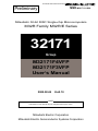
MSD-M32171-U-0008
Mitsubishi 32-bit RISC Single-chip Microcomputers
M32R Family M32R/E Series
32171
Group
M32171F4VFP
M32171F3VFP
User’s Manual
2000-08-04
Ver0.10
NOTE
Information in this manual may be changed without prior notice.
Mitsubishi Electric Corporation
Mitsubishi Electric Semiconductor Systems Corporation
PREFACE
This manual describes the hardware specifications of Mitsubishi’s 32171 group of 32-bit
CMOS microcomputers.
This manual was created to help you understand the hardware specifications of the
32171-group microcomputers so you can take
full advantage of the versatile performance capabilities of these microcomputers. The CPU
features and the functionality of each internal
peripheral circuit are described in detail, which
we hope will prove useful for your circuit design.
For details about the M32R-family software
products and development support tools,
please refer to the user’s manuals and related
other documentation included with your products and tools.
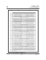
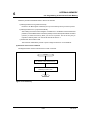
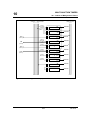
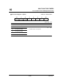
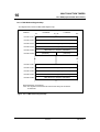
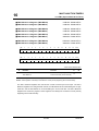
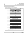
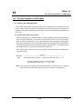
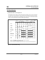
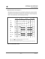
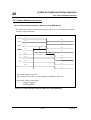
How to read internal I/O register tables
➀ Bit Numbers: Each register is connected with an internal bus of 16-bit
wide, so the bit numbers of the registers located at even
addresses are D0-D7, and those at odd addresses are
D8-D15.
➁ State of Register at Reset: Represents the initial state of each register
immediately after reset with hexadecimal numbers
(undefined bits after reset are indicated each in column ➂.)
➂ At read:
... read enabled
? ... read disabled (read value invalid)
0 ... Read always as 0
1 ... Read always as 1
④ At write:
: Write enabled
: Write enable conditionally
(include some conditions at write)
: Write disabled (Written value invalid)
-
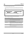
<Example of representation>
Registers represented with thick rectangles
are accessible only with halfwords or words
(not accessible with bytes).
Not implemented
in the shaded portion.
D0
1
1
2
3
4
Abit
Bbit
Cbit
2
D
Bit name
0
Not assigned.
1
2
3
Function
<at reset: H'04>
R
W
0
Abit
0: -----
(...................)
1: -----
Bbit
0: -----
(...................)
1: -----
Cbit
0: -----
(...................)
1: ----3
4
Contents
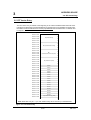
CHAPTER 1 OVERVIEW
1.1 Outline of the 32171 .......................................................................................... 1-2
1.1.1 M32R Family CPU Core .................................................................. 1-2
1.1.2 Built-in Multiply-Accumulate Operation Function ............................. 1-3
1.1.3 Built-in Flash Memory and RAM ...................................................... 1-3
1.1.4 Built-in Clock Frequency Multiplier .................................................. 1-4
1.1.5 Built-in Powerful Peripheral Functions ............................................. 1-4
1.1.6 Built-in Full-CAN Function ............................................................... 1-6
1.1.7 Built-in Debug Function ................................................................... 1-6
1.2 Block Diagram ................................................................................................... 1-7
1.3 Pin Function .................................................................................................... 1-10
1.4 Pin Layout ........................................................................................................ 1-16
CHAPTER 2 CPU
2.1 CPU Registers ................................................................................................... 2-2
2.2 General-purpose Registers .............................................................................. 2-2
2.3 Control Registers .............................................................................................. 2-3
2.3.1 Processor Status Word Register: PSW (CR0) ................................. 2-4
2.3.2 Condition Bit Register: CBR (CR1) .................................................. 2-5
2.3.3 Interrupt Stack Pointer: SPI (CR2) ................................................... 2-5
User Stack Pointer: SPU (CR3)
2.3.4 Backup PC: BPC (CR6) ................................................................... 2-5
2.4 Accumulator ...................................................................................................... 2-6
2.5 Program Counter .............................................................................................. 2-6
2.6 Data Formats ..................................................................................................... 2-7
2.6.1 Data Types ...................................................................................... 2-7
2.6.2 Data Formats ................................................................................... 2-8
(1)
CHAPTER 3 ADDRESS SPACE
3.1 Outline of Address Space ................................................................................ 3-2
3.2 Operation Modes ............................................................................................... 3-5
3.3 Internal ROM Area and Extended External Area ............................................ 3-7
3.3.1 Internal ROM Area ........................................................................... 3-7
3.3.2 Extended External Area ................................................................... 3-7
3.4 Internal RAM Area and SFR Area .................................................................... 3-8
3.4.1 Internal RAM Area ........................................................................... 3-8
3.4.2 Special Function Register (SFR) Area ............................................. 3-8
3.5 EIT Vector Entry .............................................................................................. 3-22
3.6 ICU Vector Table ............................................................................................. 3-23
3.7 Note about Address Space ............................................................................ 3-25
CHAPTER 4 EIT
4.1 Outline of EIT ..................................................................................................... 4-2
4.2 EIT Event ............................................................................................................ 4-3
4.2.1 Exception ......................................................................................... 4-3
4.2.2 Interrupt ........................................................................................... 4-3
4.2.3 Trap ................................................................................................. 4-3
4.3 EIT Processing Procedure ............................................................................... 4-4
4.4 EIT Processing Mechanism ............................................................................. 4-6
4.5 Acceptance of EIT Event .................................................................................. 4-7
4.6 Saving and Restoring the PC and PSW .......................................................... 4-8
4.7 EIT Vector Entry .............................................................................................. 4-10
4.8 Exception Processing .................................................................................... 4-11
4.8.1 Reserved Instruction Exception (RIE) ............................................ 4-11
4.8.2 Address Exception (AE) ................................................................. 4-13
4.9 Interrupt Processing ....................................................................................... 4-15
4.9.1 Reset Interrupt (RI) ........................................................................ 4-15
4.9.2 System Break Interrupt (SBI) ......................................................... 4-16
4.9.3 External Interrupt (EI) .................................................................... 4-18
(2)
4.10 Trap Processing ............................................................................................ 4-20
4.10.1 Trap (TRAP) ................................................................................ 4-20
4.11 EIT Priority Levels ......................................................................................... 4-22
4.12 Example of EIT Processing .......................................................................... 4-23
CHAPTER 5 INTERRUPT CONTROLLER (ICU)
5.1 Outline of Interrupt Controller (ICU) ................................................................ 5-2
5.2 Interrupt Sources of Internal Peripheral I/Os ................................................. 5-4
5.3 ICU-Related Registers ...................................................................................... 5-5
5.3.1 Interrupt Vector Register .................................................................. 5-6
5.3.2 Interrupt Mask Register ................................................................... 5-7
5.3.3 SBI (System Break Interrupt) Control Register ................................ 5-8
5.3.4 Interrupt Control Registers ............................................................... 5-9
5.4 ICU Vector Table ............................................................................................. 5-13
5.5 Description of Interrupt Operation ................................................................ 5-16
5.5.1 Acceptance of Internal Peripheral I/O Interrupts ............................ 5-16
5.5.2 Processing of Internal Peripheral I/O Interrupts by Handlers ........ 5-19
5.6 Description of System Break Interrupt (SBI) Operation .............................. 5-21
5.6.1 Acceptance of SBI ......................................................................... 5-21
5.6.2 SBI Processing by Handler ............................................................ 5-21
CHAPTER 6 INTERNAL MEMORY
6.1 Outline of the Internal Memory ........................................................................ 6-2
6.2 Internal RAM ...................................................................................................... 6-2
6.3 Internal Flash Memory ...................................................................................... 6-2
6.4 Registers Associated with the Internal Flash Memory .................................. 6-3
6.4.1 Flash Mode Register ........................................................................ 6-4
6.4.2 Flash Status Registers ..................................................................... 6-5
6.4.3 Flash Controle Registers ................................................................. 6-8
6.4.4 Virtual Flash L Bank Registers ...................................................... 6-14
6.4.5 Virtual Flash S Bank Registers ...................................................... 6-15
6.5 Programming of the Internal Flash Memory ................................................. 6-16
(3)
6.5.1 Outline of Programming Flash Memory ......................................... 6-16
6.5.2 Controlling Operation Mode during Programming Flash ............... 6-22
6.5.3 Programming Procedure to the Internal Flash Memory ................. 6-25
6.5.4 Flash Write Time (for Reference) .................................................. 6-38
6.6 Boot ROM ........................................................................................................ 6-39
6.7 Virtual Flash Emulation Function .................................................................. 6-40
6.7.1 Virtual Flash Emulation Area ......................................................... 6-41
6.7.2 Entering Virtual Flash Emulation Mode ......................................... 6-46
6.7.3 Application Example of Virtual Flash Emulation Mode .................. 6-47
6.8 Connecting to A Serial Programmer ............................................................. 6-49
6.9 Precautions to Be Taken When Rewriting Flash Memory ........................... 6-51
CHAPTER 7 RESET
7.1 Outline of Reset ................................................................................................ 7-2
7.2 Reset Operation ................................................................................................ 7-2
7.2.1 Reset at Power-on ........................................................................... 7-2
7.2.2 Reset during Operation .................................................................... 7-2
7.2.3 Reset Vector Relocation during Flash Rewrite ................................ 7-2
7.3 Internal State Immediately after Reset Release ............................................. 7-3
7.4 Things To Be Considered after Reset Release .............................................. 7-4
CHAPTER 8 INPUT/OUTPUT PORTS AND PIN FUNCTIONS
8.1 Outline of Input/Output Ports .......................................................................... 8-2
8.2 Selecting Pin Functions ................................................................................... 8-4
8.3 Input/Output Port Related Registers ............................................................... 8-6
8.3.1 Port Data Registers ......................................................................... 8-8
8.3.2 Port Direction Registers ................................................................... 8-9
8.3.3 Port Operation Mode Registers ..................................................... 8-10
8.4 Port Peripheral Circuits .................................................................................. 8-22
CHAPTER 9 DMAC
9.1 Outline of the DMAC ......................................................................................... 9-2
(4)
9.2 DMAC Related Registers .................................................................................. 9-4
9.2.1 DMA Channel Control Register ....................................................... 9-6
9.2.2 DMA Software Request Generation Registers .............................. 9-17
9.2.3 DMA Source Address Registers .................................................... 9-18
9.2.4 DMA Destination Address Registers ............................................. 9-19
9.2.5 DMA Transfer Count Registers ...................................................... 9-20
9.2.6 DMA Interrupt Request Status Registers ....................................... 9-21
9.2.7 DMA Interrupt Mask Registers ....................................................... 9-23
9.3 Functional Description of the DMAC ............................................................ 9-27
9.3.1 Cause of DMA Request ................................................................. 9-27
9.3.2 DMA Transfer Processing Procedure ............................................ 9-31
9.3.3 Starting DMA ................................................................................. 9-32
9.3.4 Channel Priority ............................................................................. 9-32
9.3.5 Gaining and Releasing Control of the Internal Bus ........................ 9-32
9.3.6 Transfer Units ................................................................................ 9-33
9.3.7 Transfer Counts ............................................................................. 9-33
9.3.8 Address Space .............................................................................. 9-33
9.3.9 Transfer Operation ......................................................................... 9-33
9.3.10 End of DMA and Interrupt ............................................................ 9-37
9.3.11 Status of Each Register after Completion of DMA Transfer ........ 9-37
9.4 Precautions about the DMAC ........................................................................ 9-38
CHAPTER 10 MULTIJUNCTION TIMERS
10.1 Outline of Multijunction Timers ................................................................... 10-2
10.2 Common Units of Multijunction Timer ........................................................ 10-7
10.2.1 Timer Common Register Map ...................................................... 10-7
10.2.2 Prescaler Unit .............................................................................. 10-9
10.2.3 Clock Bus/Input-Output Event Bus Control Unit ........................ 10-10
10.2.4 Input Processing Control Unit .................................................... 10-15
10.2.5 Output Flip-Flop Control Unit ..................................................... 10-21
10.2.6 Interrupt Control Unit ................................................................. 10-29
10.3 TOP (Output-related 16-bit Timer) ............................................................. 10-45
10.3.1 Outline of TOP ........................................................................... 10-45
10.3.2 Outline of Each Mode of TOP .................................................... 10-47
10.3.3 TOP Related Register Map ........................................................ 10-49
(5)
10.3.4 TOP Control Registers ............................................................... 10-52
10.3.5 TOP Counters (TOP0CT-TOP10CT) ......................................... 10-59
10.3.6 TOP Reload Registers (TOP0RL-TOP10RL) ............................ 10-60
10.3.7 TOP Correction Registers (TOP0CC-TOP10CC) ..................... 10-61
10.3.8 TOP Enable Control Register .................................................... 10-62
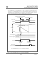
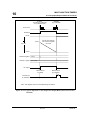
10.3.9 Operation in TOP Single-shot Output Mode (with Correction Function) ......... 10-66
10.3.10 Operation in TOP Delayed Single-shot Output Mode (With Correction Function) ...... 10-73
10.3.11 Operation in TOP Continuous Output Mode (Without Correction Function) .............. 10-78
10.4 TIO (Input/Output-related 16-bit Timer) ..................................................... 10-82
10.4.1 Outline of TIO ............................................................................ 10-82
10.4.2 Outline of Each Mode of TIO ..................................................... 10-84
10.4.3 TIO Related Register Map ......................................................... 10-87
10.4.4 TIO Control Registers ................................................................ 10-90
10.4.5 TIO Counter (TIO0CT-TIO9CT) ............................................... 10-101
10.4.6 TIO Reload 0/ Measure Register (TIO0RL0-TIO9RL0) ........... 10-102
10.4.7 TIO Reload 1 Registers (TIO0RL1-TIO9RL1) ......................... 10-103
10.4.8 TIO Enable Control Registers .................................................. 10-104
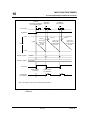
10.4.9 Operation in TIO Measure Free-run/Clear Input Modes .......... 10-107
10.4.10 Operation in TIO Noise Processing Input Mode ..................... 10-111
10.4.11 Operation in TIO PWM Output Mode ...................................... 10-112
10.4.12 Operation in TIO Single-shot Output Mode (without Correction Function) .. 10-116
10.4.13 Operation in TIO Delayed Single-shot Output Mode (without Correction Function) .. 10-118
10.4.14 Operation in TIO Continuous Output Mode (Without Correction Function) 10-120
10.5 TMS (Input-related 16-bit Timer) .............................................................. 10-122
10.5.1 Outline of TMS ......................................................................... 10-122
10.5.2 Outline of TMS Operation ........................................................ 10-122
10.5.3 TMS Related Register Map ..................................................... 10-124
10.5.4 TMS Control Registers ............................................................ 10-125
10.5.5 TMS Counter (TMS0CT, TMS1CT) ......................................... 10-127
10.5.6 TMS Measure Registers (TMS0MR3-0, TMS1MR3-0) ............ 10-128
10.5.7 Operation of TMS Measure Input ............................................ 10-129
10.6 TML (Input-related 32-bit Timer) .............................................................. 10-131
10.6.1 Outline of TML ......................................................................... 10-131
10.6.2 Outline of TML Operation ........................................................ 10-132
10.6.3 TML Related Register Map ...................................................... 10-133
10.6.4 TML Control Registers ............................................................. 10-134
(6)
10.6.5 TML Counters .......................................................................... 10-136
10.6.6 TML Measure Registers .......................................................... 10-138
10.6.7 Operation of TML Measure Input ............................................. 10-140
CHAPTER 11 A-D CONVERTERS
11.1 Outline of A-D Converter .............................................................................. 11-2
11.1.1 Conversion Modes ....................................................................... 11-5
11.1.2 Operation Modes ......................................................................... 11-6
11.1.3 Special Operation Modes .......................................................... 11-10
11.1.4 A-D Converter Interrupt and DMA Transfer Requests ............... 11-13
11.2 A-D Converter Related Registers .............................................................. 11-14
11.2.1 A-D Single Mode Register 0 ...................................................... 11-16
11.2.2 A-D Single Mode Register 1 ...................................................... 11-19
11.2.3 A-D Scan Mode Register 0 ........................................................ 11-21
11.2.4 A-D Scan Mode Register 1 ........................................................ 11-24
11.2.5 A-D Successive Approximation Register ................................... 11-26
11.2.6 A-D0 Comparate Data Register .................................................. 11-27
11.2.7 10-bit A-D Data Registers .......................................................... 11-28
11.2.8 8-bit A-D Data Registers ............................................................ 11-29
11.3 Functional Description of A-D Converters ............................................... 11-30
11.3.1 How to Find Along Input Voltages ............................................. 11-30
11.3.2 A-D Conversion by Successive Approximation Method ............ 11-31
11.3.3 Comparator Operation ............................................................... 11-33
11.3.4 Calculation of the A-D Conversion Time .................................... 11-34
11.3.5 Definition of the A-D Conversion Accuracy ................................ 11-37
11.4 Precautions on Using A-D Converters ...................................................... 11-40
CHAPTER 12 SERIAL I/O
12.1 Outline of Serial I/O ....................................................................................... 12-2
12.2 Serial I/O Related Registers ......................................................................... 12-6
12.2.1 SIO Interrupt Related Registers ................................................... 12-7
12.2.2 SIO Interrupt Control Registers ................................................... 12-9
12.2.3 SIO Transmit Control Registers ................................................. 12-13
12.2.4 SIO Transmit/Receive Mode Registers ..................................... 12-15
(7)
12.2.5 SIO Transmit Buffer Registers ................................................... 12-18
12.2.6 SIO Receive Buffer Registers .................................................... 12-19
12.2.7 SIO Receive Control Registers .................................................. 12-20
12.2.8 SIO Baud Rate Registers .......................................................... 12-23
12.3 Transmit Operation in CSIO Mode ............................................................ 12-25
12.3.1 Setting the CSIO Baud Rate ...................................................... 12-25
12.3.2 Initial Settings for CSIO Transmission ....................................... 12-26
12.3.3 Starting CSIO Transmission ...................................................... 12-28
12.3.4 Successive CSIO Transmission ................................................ 12-28
12.3.5 Processing at End of CSIO Transmission ................................. 12-29
12.3.6 Transmit Interrupt ...................................................................... 12-29
12.3.7 Transmit DMA Transfer Request ............................................... 12-29
12.3.8 Typical CSIO Transmit Operation .............................................. 12-31
12.4 Receive Operation in CSIO Mode .............................................................. 12-33
12.4.1 Initial Settings for CSIO Reception ............................................ 12-33
12.4.2 Starting CSIO Reception ........................................................... 12-35
12.4.3 Processing at End of CSIO Reception ....................................... 12-35
12.4.4 About Successive Reception ..................................................... 12-36
12.4.5 Flags Indicating the Status of CSIO Receive Operation ............ 12-37
12.4.6 Typical CSIO Receive Operation ............................................... 12-38
12.5 Precautions on Using CSIO Mode ............................................................. 12-40
12.6 Transmit Operation in UART Mode ........................................................... 12-42
12.6.1 Setting the UART Baud Rate ..................................................... 12-42
12.6.2 UART Transmit/Receive Data Formats ..................................... 12-43
12.6.3 Initial Settings for UART Transmission ...................................... 12-45
12.6.4 Starting UART Transmission ..................................................... 12-47
12.6.5 Successive UART Transmission ............................................... 12-47
12.6.6 Processing at End of UART Transmission ................................ 12-48
12.6.7 Transmit Interrupt ...................................................................... 12-48
12.6.8 Transmit DMA Transfer Request ............................................... 12-48
12.6.9 Typical UART Transmit Operation ............................................. 12-50
12.7 Receive Operation in UART Mode ............................................................. 12-52
12.7.1 Initial Settings for UART Reception ........................................... 12-52
12.7.2 Starting UART Reception .......................................................... 12-54
12.7.3 Processing at End of UART Reception ...................................... 12-54
(8)
12.7.4 Typical UART Receive Operation .............................................. 12-56
12.8 Fixed Period Clock Output Function ......................................................... 12-58
12.9 Precautions on Using UART Mode ............................................................ 12-59
CHAPTER 13 CAN MODULE
13.1 Outline of the CAN Module .......................................................................... 13-2
13.2 CAN Module Related Registers ................................................................... 13-4
13.2.1 CAN Control Register .................................................................. 13-8
13.2.2 CAN Status Register .................................................................. 13-11
13.2.3 CAN Extended ID Register ........................................................ 13-15
13.2.4 CAN Configuration Register ...................................................... 13-16
13.2.5 CAN Time Stamp Count Register .............................................. 13-19
13.2.6 CAN Error Count Registers ....................................................... 13-20
13.2.7 CAN Baud Rate Prescaler ......................................................... 13-21
13.2.8 CAN Interrupt Related Registers ............................................... 13-22
13.2.9 CAN Mask Registers ................................................................. 13-30
13.2.10 CAN Message Slot Control Registers ...................................... 13-34
13.2.11 CAN Message Slots ................................................................. 13-38
13.3 CAN Protocol ............................................................................................... 13-53
13.3.1 CAN Protocol Frame .................................................................. 13-53
13.4 Initializing the CAN Module ........................................................................ 13-56
13.4.1 Initialization of the CAN Module ................................................. 13-56
13.5 Transmitting Data Frames .......................................................................... 13-59
13.5.1 Data Frame Transmit Procedure ............................................... 13-59
13.5.2 Data Frame Transmit Operation ................................................ 13-61
13.5.3 Transmit Abort Function ............................................................ 13-62
13.6 Receiving Data Frames .............................................................................. 13-63
13.6.1 Data Frame Receive Procedure ................................................ 13-63
13.6.2 Data Frame Receive Operation ................................................. 13-65
13.6.3 Reading Out Received Data Frames ......................................... 13-67
13.7 Transmitting Remote Frames .................................................................... 13-69
13.7.1 Remote Frame Transmit Procedure .......................................... 13-69
13.7.2 Remote Frame Transmit Operation ........................................... 13-71
13.7.3 Reading Out Received Data Frames when Set for Remote Frame Transmission ...... 13-74
(9)
13.8 Receiving Remote Frames ......................................................................... 13-76
13.8.1 Remote Frame Receive Procedure ........................................... 13-76
13.8.2 Remote Frame Receive Operation ............................................ 13-78
CHAPTER 14 REAL-TIME DEBUGGER (RTD)
14.1 Outline of the Real-Time Debugger (RTD) .................................................. 14-2
14.2 Pin Function of the RTD ............................................................................... 14-3
14.3 Functional Description of the RTD .............................................................. 14-4
14.3.1 Outline of RTD Operation ............................................................ 14-4
14.3.2 Operation of RDR (Real-time RAM Content Output) ................... 14-5
14.3.3 Operation of WRR (RAM Content Forcible Rewrite) ................... 14-7
14.3.4 Operation of VER (Continuous Monitor) ...................................... 14-9
14.3.5 Operation of VEI (Interrupt Request) ......................................... 14-10
14.3.6 Operation of RCV (Recover from Runaway) ............................. 14-11
14.3.7 Method to Set a Specified Address when Using the RTD ......... 14-12
14.3.8 Resetting the RTD ..................................................................... 14-13
14.4 Typical Connection with the Host ............................................................. 14-14
CHAPTER 15 EXTERNAL BUS INTERFACE
15.1 External Bus Interface Related Signals ...................................................... 15-2
15.2 Read/Write Operations ................................................................................. 15-6
15.3 Bus Arbitration ............................................................................................ 15-12
15.4 Typical Connection of External Extension Memory ................................ 15-14
CHAPTER 16 WAIT CONTROLLER
16.1 Outline of the Wait Controller ...................................................................... 16-2
16.2 Wait Controller Related Registers ............................................................... 16-4
16.2.1 Wait Cycles Control Register ....................................................... 16-5
16.3 Typical Operation of the Wait Controller .................................................... 16-6
(10)
CHAPTER 17 RAM BACKUP MODE
17.1 Outline ............................................................................................................ 17-2
17.2 Example of RAM Backup when Power is Down ......................................... 17-2
17.2.1 Normal Operating State ............................................................... 17-3
17.2.2 RAM Backup State ...................................................................... 17-4
17.3 Example of RAM Backup for Saving Power Consumption ....................... 17-5
17.3.1 Normal Operating State ............................................................... 17-6
17.3.2 RAM Backup State ...................................................................... 17-7
17.3.3 Precautions to Be Observed at Power-on ................................... 17-8
17.4 Exiting RAM Backup Mode (Wakeup) ......................................................... 17-9
CHAPTER 18 OSCILLATION CIRCUIT
18.1 Oscillator Circuit ........................................................................................... 18-2
18.1.1 Example of an Oscillator Circuit ................................................... 18-2
18.1.2 System Clock Output Function .................................................... 18-3
18.1.3 Oscillation Stabilization Time at Power-on .................................. 18-4
18.2 Clock Generator Circuit ................................................................................ 18-5
CHAPTER 19 JTAG
19.1 Outline of JTAG ............................................................................................. 19-2
19.2 Configuration of the JTAG Circuit ............................................................... 19-3
19.3 JTAG Registers ............................................................................................. 19-4
19.3.1 Instruction Register (JTAGIR) ...................................................... 19-4
19.3.2 Data Registers ............................................................................. 19-5
19.4 Basic Operation of JTAG ............................................................................. 19-6
19.4.1 Outline of JTAG Operation .......................................................... 19-6
19.4.2 IR Path Sequence ........................................................................ 19-8
19.4.3 DR Path Sequence .................................................................... 19-10
19.4.4 Examining and Setting Data Registers ...................................... 19-12
19.5 Boundary Scan Description Language ..................................................... 19-14
19.6 Precautions about Board Design when Connecting JTAG ..................... 19-29
(11)
CHAPTER 20 POWER-UP/POWER-SHUTDOWN SEQUENCE
20.1 Configuration of the Power Supply Circuit ................................................ 20-2
20.2 Power-On Sequence ..................................................................................... 20-3
20.2.1 Power-On Sequence When Not Using RAM Backup .................. 20-3
20.2.2 Power-On Sequence When Using RAM Backup ......................... 20-4
20.3 Power-Shutdown Sequence ......................................................................... 20-5
20.3.1 Power-Shutdown Sequence When Not Using RAM Backup ....... 20-5
20.3.2 Power-Shutdown Sequence When Using RAM Backup .............. 20-6
CHAPTER 21 ELECTRICAL CHARACTERISTICS
21.1 Absolute Maximum Ratings ......................................................................... 21-2
21.2 Recommended Operating Conditions ........................................................ 21-3
21.3 DC Characteristics ........................................................................................ 21-5
21.3.1 Electrical Characteristics ............................................................. 21-5
21.3.2 Flash Related Electrical Characteristics .................................... 21-10
21.4 A-D Conversion Characteristics ................................................................ 21-11
21.5 AC Characteristics ...................................................................................... 21-12
21.5.1 Timing Requirements ................................................................. 21-12
21.5.2 Switching Characteristics ........................................................... 21-15
21.5.3 AC Characteristics ..................................................................... 21-18
CHAPTER 22 TYPICAL CHARACTERISTICS
22.1 A-D Conversion Characteristics .................................................................. 22-2
APPENDIX 1 MECHANICAL SPECIFICATIONS
Appendix 1.1 Dimensional Outline Drawing ....................................... Appendix 1-2
APPENDIX 2 INSTRUCTION PROCESSING TIME
Appendix 2.1 32170 Instruction Processing Time ............................. Appendix 2-2
(12)
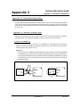
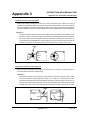
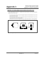
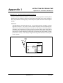
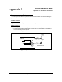
APPENDIX 3 PRECAUTIONS ABOUT NOISE
Appendix 3.1 Precautions about Noise .............................................. Appendix 3-2
Appendix 3.1.1 Reduction of Wiring Length ...................................... Appendix 3-2
Appendix 3.1.2 Inserting a Bypass Capacitor between VSS and VCC Lines ... Appendix 3-4
Appendix 3.1.3 Processing Analog Input Pin Wiring ........................ Appendix 3-5
Appendix 3.1.4 Consideration about the Oscillator ........................... Appendix 3-6
Appendix 3.1.5 Processing Input/Output Ports ................................. Appendix 3-8
(13)
❊ This is a blank page. ❊
(14)
CHAPTER 1
OVERVIEW
1.1
1.2
1.3
1.4
Outline of the 32171
Block Diagram
Pin Function
Pin Layout
OVERVIEW
1
1.1 Outline of the 32171
1.1 Outline of the 32171
1.1.1 M32R Family CPU Core
(1) Based on RISC architecture
• The 32171 is a 32-bit RISC single-chip microcomputer which is built around the M32R family
CPU core (hereafter referred to as the M32R) and incorporates flash memory, RAM, and
various other peripheral functions-all integrated into a single chip.
• The M32R is based on RISC architecture. Memory access is performed using load and store
instructions, and various arithmetic operations are executed using register-to-register
operation instructions. The M32R internally contains sixteen 32-bit general-purpose registers
and has 83 distinct instructions.
• The M32R supports compound instructions such as Load & Address Update and Store &
Address Update, in addition to ordinary load and store instructions. These compound
instructions help to speed up data transfers.
(2) 5-stage pipelined processing
• The M32R uses 5-stage pipelined instruction processing consisting of Instruction Fetch,
Decode, Execute, Memory Access, and Write Back. Not just load and store instructions or
register-to-register operation instructions, compound instructions such as Load & Address
Update and Store & Address Update also are executed in one cycle.
• Instructions are entered into the execution stage in the order they are fetched, but this does not
always mean that the first instruction entered is executed first. If the execution of a load or
store instruction entered earlier is delayed by one or more wait cycles inserted in memory
access, a register-to-register operation instruction entered later may be executed before said
load or store instruction. By using "out-of-order-completion" like this, the M32R controls
instruction execution without wasting clock cycles.
(3) Compact instruction code
• The M32R instructions come in two types: one consisting of 16 bits in length, and the other
consisting of 32 bits in length. Use of the 16-bit length instruction format especially helps to
suppress the program code size.
• Some 32-bit long instructions can branch directly to a location 32 Mbytes forward or backward
from the instruction address being executed. Compared to architectures where address space
is segmented, this direct jump allows for easy programming.
1-2
Ver.0.10
OVERVIEW
1
1.1 Outline of the 32171
1.1.2 Built-in Multiply-Accumulate Operation Function
(1) Built-in high-speed multiplier
• The M32R incorporates a 32-bit × 16-bit high-speed multiplier which enables it to execute a
32-bit × 32-bit integral multiplication instruction in three cycles (1 cycle = 25 ns when using a 40
MHz internal CPU clock).
(2) Supports Multiply-Accumulate operation instructions comparable to DSP
• The M32R supports the following four modes of Multiply-Accumulate operation instructions (or
multiplication instructions) using a 56-bit accumulator. Any of these operations can be
executed in one cycle.
➀ 16 high-order register bits × 16 high-order register bits
➁ 16 low-order register bits × 16 low-order register bits
➂ Entire 32 register bits × 16 high-order register bits
➃ Entire 32 register bits × 16 low-order register bits
• The M32R has instructions to round off the value stored in the accumulator to 16 or 32 bits, as
well as instructions to shift the accumulator value to adjust digits and store the digit-adjusted
value in a register. These instructions also can be executed in one cycle, so that when
combined with high-speed data transfer instructions such as Load & Address Update and
Store & Address Update, they enable the M32R to exhibit high data processing capability
comparable to that of DSP.
1.1.3 Built-in Flash Memory and RAM
• The 32171 contains flash memory and RAM which can be accessed with no wait states,
allowing you to build a high-speed embedded system.
• The internal flash memory allows for on-board programming (you can write to it while being
mounted on the printed circuit board). Use of flash memory means the chip engineered at the
development phase can be used directly in mass-production, so that you can smoothly
migrate from prototype to mass-production without changing the printed circuit board.
• The internal flash memory can be rewritten 100 times.
• The internal flash memory has a pseudo-flash emulation function, allowing the internal RAM to
be artificially mapped into part of the internal flash memory. This function, when combined with
the internal Real-Time Debugger (RTD), facilitates data tuning on ROM tables.
• The internal RAM can be accessed for read or rewrite from an external device independently
of the M32R by using RTD (real-time debugger). It is communicated with external devices by
RTD's exclusive clock-synchronized serial I/O.
1-3
Ver.0.10
OVERVIEW
1
1.1 Outline of the 32171
1.1.4 Built-in Clock Frequency Multiplier
• The 32171 internally multiplies the input clock signal frequency by 4 and the internal peripheral
clock by 2. If the input clock frequency is 10.0 MHz, the CPU clock frequency will be 40 MHz
and the internal clock frequency 20 MHz.
1.1.5 Built-in Powerful Peripheral Functions
(1) Built-in multijunction timer (MJT)
• The multijunction timer is configured with the following 37 channels timers:
➀ 16-bit output-related timer × 11 channels
➁ 16-bit input/output-related timer × 10 channels
➂ 16-bit input-related timer × 8 channels (incorporating three channels of multiply-by-4
counter)
➃ 32-bit input-related timer × 8 channels
Each timer has multiple modes of operation, which can be selected according of the purpose of use.
• The multijunction timer has internal clock bus, input event bus, and output event bus, allowing
multiple timers to be combined for use internally. This provides a flexible way to make use of
timer functions.
• The output-related timers (TOP) have a correction function. This function allows the timer's
count value in progress to be increased or reduced as desired, thus materializing real-time
output control.
(2) Built-in 10-channel DMA
• The 10-channel DMA is built-in, supporting data transfers between internal peripheral I/Os or
between internal peripheral I/O and internal RAM. Not only can DMA transfer requests be
generated in software, but can also be triggered by a signal generated by an internal
peripheral I/O (e.g., A-D converter, MJT, or serial I/O).
• Cascaded connection between DMA channels (DMA transfer in a channel is started by
completion of transfer in another) is also supported, allowing for high-speed transfer
processing without imposing any extra load on the CPU.
(3) Built-in 16-channel A-D converters
• The 32171 contains one 16-channel A-D converters which can convert data in 10-bit
resolution. In addition to single A-D conversion in each channel, successive A-D conversion in
four, eight, or 16 channels combined into one unit is possible.
• In addition to ordinary A-D conversion, a comparator mode is supported in which the A-D
conversion result is compared with a given set value to determine the relative magnitudes of
two quantities.
• When A-D conversion is completed, the 32171 can generate not only an interrupt, but can also
generate a DMA transfer request.
• The 32171 supports two read out modes, so that A-D conversion results can be read out in 8
bits or 10 bits.
1-4
Ver.0.10
OVERVIEW
1
1.1 Outline of the 32171
(4) High-speed serial I/O
• The 32171 incorporates 3 channels of serial I/O, which can be set for clock-synchronized
serial I/O or UART.
• When set for clock-synchronized serial I/O, the data transfer rate is a high 2 Mbits per second.
• When data reception is completed or the transmit buffer becomes empty, the serial I/O can
generate a DMA transfer request signal.
(5) Built-in Real-Time Debugger (RTD)
• The Real-Time Debugger (RTD) provides a function for the M32R/E's internal RAM to be
accessed directly from an external device. The debugger communicates with external devices
through its exclusive clock-synchronized serial I/O.
• By using the RTD, you can read the contents of the internal RAM or rewrite its data from an
external device independently of the M32R.
• The debugger can generate an RTD interrupt to notify that RTD-based data transmission or
reception is completed.
(6) Eight-level interrupt controller
• The interrupt controller manages interrupt requests from each internal peripheral I/O by
resolving interrupt priority in eight levels including an interrupt-disabled state. Also, it can
accept external interrupt requests due to power-down detection or generated by a watchdog
timer as a System Break Interrupt (SBI).
(7) Three operation modes
• The M32R/E has three operation modes-single-chip mode, extended external mode, and
processor mode. The address space and external pin functions of the M32R/E are switched
over according to a mode in which it operates. The MOD0 and MOD1 pins are used to set a
mode.
(8) Wait controller
• The wait controller supports access to external devices by the M32R. In all but single-chip
mode, the extended external area provides 4 Mbytes of space.
1-5
Ver.0.10
OVERVIEW
1
1.1 Outline of the 32171
1.1.6 Built-in Full-CAN Function
• The 32171 contains CAN Specification V2.0B-compliant CAN module, thereby providing 16
message slots.
1.1.7 Built-in Debug Function
• The 32171 supports JTAG interface. Boundary scan test can be performed using this JTAG
interface.
1-6
Ver.0.10
OVERVIEW
1
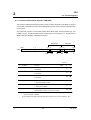
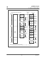
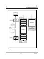
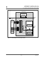
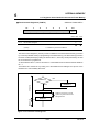
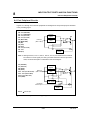
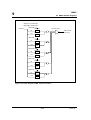
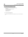
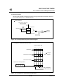
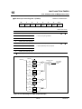
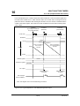
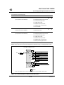
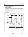
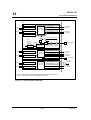
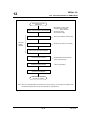
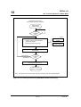
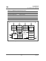
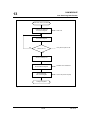
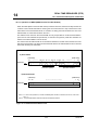
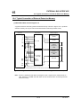
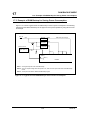
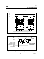
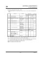
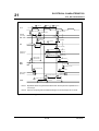
1.2 Block Diagram
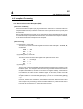
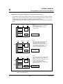
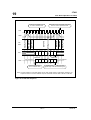
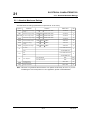
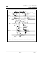
1.2 Block Diagram
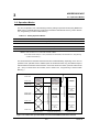
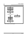
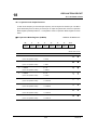
Figure 1.2.1 shows a block diagram of the 32171. Features of each block are shown in Tables 1.2.1
through 1.2.3.
32171
Internal bus interface
M32R CPU core
(max 40 MHz)
DMA C
(10 channels)
Multiplieraccumulator
(32 X 16 + 56)
Internal 32-bit bus
Multijunction timer
(MJT: 37 channels)
A-D converter
(10-bit resolution, 16 channels)
Internal 16-bit bus
Internal flash memory
(M32171F4:512KB)
(M32171F3:384KB)
Serial I/O
(3 channels)
Interrupt controller
(22 sources, 8 levels)
Internal RAM
(16KB)
Wait controller
Full CAN
(1 channel)
Real-time debugger ( RTD)
External bus
interface
PLL clock generator circuit
Data
Address
Input/output port (JTAG), 97 lines
Figure 1.2.1 Block Diagram of the 32171
1-7
Ver.0.10
OVERVIEW
1
1.2 Block Diagram
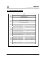
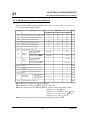
Table 1.2.1 Features of the M32R Family CPU Core
Functional Block
Features
M32R family
• Bus specifications
CPU core
Basic bus cycle: 25 ns (when operating with 40 MHz CPU clock)
Logical address space: 4Gbytes, linear
Extended external area: Maximum 4 Mbytes
External data bus: 16 bits
• Implementation: Five-stage pipeline
• Internal 32-bit architecture for the core
• Register configuration
General-purpose register: 32 bits × 16 registers
Control register: 32 bits × 5 registers
• Instruction set
16-bit and 32-bit instruction formats
83 distinct instructions and 9 addressing modes
• Built-in multiplier/accumulator (32 × 16 + 56)
Table 1.2.2 Features of Internal Memory
Functional Block
Features
RAM
• Capacity : 16 Kbytes
• No-wait access (when operating with 40 MHz CPU clock)
• By using RTD (real-time debugger), the internal RAM can be accessed for read or
rewrite from external devices independently of the M32R.
Flash memory
• Capacity
M32171F4 : 512 Kbytes
M32171F3 : 384 Kbytes
• No-wait access (when operating with 40 MHz CPU clock)
• Durability: Can be rewritten 100 times
1-8
Ver.0.10
OVERVIEW
1
1.2 Block Diagram
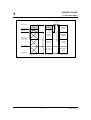
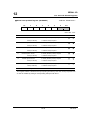
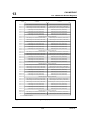
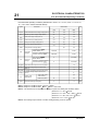
Table 1.2.3 Features of Internal Peripheral I/O
Functional Block
Features
DMA
• 10-channel DMA
• Supports transfer between internal peripheral I/Os and between internal peripheral I/O
and internal RAM.
• Capable of advanced DMA transfer when operating in combination with internal
peripheral I/O
• Capable of cascaded connection between DMA channels (DMA transfer in a channel
is started by completion of transfer in another)
Multijunction
• 37-channel multifunction timer
• Contains output-related timer × 11 channels, input/output-related timer × 10 channels,
16-bit input-related timer × 8 channels, and 32-bit input-related timer × 8 channels.
• Capable of flexible timer configuration by mutual connection between each channel.
A-D converter
• 16-channel, 10-bit resolution A-D converter
• Incorporates comparator mode
• Can generate interrupt or start DMA transfer upon completion of A-D conversion.
• Can read out conversion results in 8 or 10 bits.
Serial I/O
• 3-channel serial I/O
• Can be set for clock-synchronized serial I/O or UART.
• Capable of high-speed data transfer at 2 Mbits per second when clock synchronized or
156 Kbits per second during UART.
Real-time debugger • Can rewrite or monitor the internal RAM independently of the CPU by command input
from an external source.
• Has its exclusive clock-synchronized serial port.
Interrupt controller
• Accepts and manages interrupt requests from internal peripheral I/O.
• Resolves interrupt priority in 8 levels including interrupt-disabled state.
Wait controller
• Controls wait state for access to extended external areas.
• Can insert 1 to 4 wait cycles by setting in software and extend wait period by external
WAIT signal.
Clock PLL
• Multiply-by-4 clock generator circuit
• Maximum 40 MHz of CPU clock (CPU, internal ROM, internal RAM access)
• Maximum 20 MHz of internal peripheral clock (peripheral module access)
• Maximum external input clock frequency=10 MHz
CAN
• Sixteen message slots
JTAG
• Capable of boundary scan
1-9
Ver.0.10
OVERVIEW
1
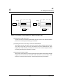
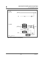
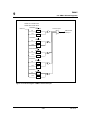
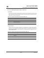
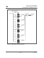
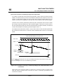
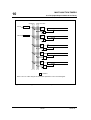
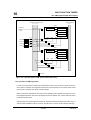
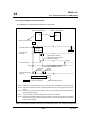
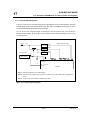
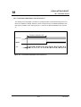
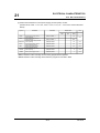
1.3 Pin Function
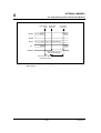
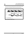
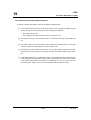
1.3 Pin Function
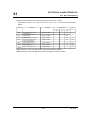
Figure 1.3.1 shows pin functions of the M32171FxVFP. Table 1.3.1 explains the pin functions.
Clock
Port 7
3.3V (Note 1)
XIN
XOUT
VCNT
OSC-VCC
OSC-VSS
P45 / CS1
P44 / CS0
P43 / RD
P42 / BHW / BHE
P41 / BLW / BLE
P71 / WAIT
P72 / HREQ
P73 / HACK
P70 / BCLK / WR
P220 / CTX
P221 / CRX
P150,P153 / TIN0,TIN3
P130- P137 / TIN16 - TIN23
Multi-junction
timer
P124 -P127 / TCLK0 -TCLK3
P93 -P97 / TO16 -TO20
P100 - P107 / TO8 - TO15
P110 - P117 / TO0 - TO7
A-D converter
Port 6
Port 6
Port 7
Interrupt
controller
AD0IN0- AD0IN15
AVCC0
AVSS0
VREF0
P61-P63
21
VCCI
Address
bus
Port 2
Port 3
Port 4
Port 22
P00 -P07 / DB0- DB7
P10-P17 / DB8 -DB15
Data
bus
Port 0
Port 1
P82 / TXD0
P83 / RXD0
P84 / SCLKI 0 / SCLKO 0
Port 8
Port 17
P174 / TXD2
P175 / RXD2
16
P74 / RTDTXD
P75 / RTDRXD
P76 / RTDACK
P77 / RTDCLK
Real-time Port 7
debugger
JTMS
JTCK
JTRST
JTDO
JTDI
JTAG
3
P64 / SBI
VCCE
P20- P27 / A23 - A30
P30 - P37 / A15 - A22
P46,P47 / A13,A14
P225 / A12 (Note2)
Serial
P85 / TXD1
I/O
P86 / RXD1
P87 / SCLKI 1 / SCLKO 1
4
3
3.3V
Port 11
Port 10
Port 9
4
3.3V
Port 15
Port 13
10
16
5V
CAN
M32171FxVFP
Mode
MOD0
MOD1
FP
5V (Note 1)
19
Port 12
Port 4
RESET
Reset
Port 22
Bus
control
VDD
FVCC
5
VSS
Note1.
3.3V
5V
: denotes blocks operating with a 3.3 V power supply.
: denotes blocks operating with a 5 V power supply.
Note2. Use caution when using this port because it has a debug event function.
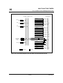
Figure 1.3.1 Pin Function Diagram of 240QFP
1-10
Ver.0.10
OVERVIEW
1
1.3 Pin Function
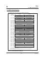
Table 1.3.1 Description of the 32171 Pin Function (1/5)
Type
Pin Name Signal Name
Input/Output Function
Power
VCCE
Power supply
—
Power supply to external I/O ports (5 V).
VCCI
Power supply
—
Power supply to internal logic (3.3 V).
VDD
RAM power supply
—
Power supply for internal RAM backup (3.3 V).
FVCC
FLASH power supply —
Power supply for internal flash memory (3.3 V).
VSS
Ground
—
Connect all VSS to ground (GND).
XIN,
Clock
Input
Clock input/output pins. These pins contains a PLL-based
Output
frequency multiplier circuit. Apply a clock whose frequency
supply
Clock
XOUT
is 1/4 the operating frequency. (When using 40 MHz CPU
clock, XIN input = 10.0 MHz)
BCLK/WR System clock
Output
This pin outputs a clock whose frequency is twice that of
external input clock. (When using 10 MHz external input
clock, BCLK output = 20 MHz). Use this output when
external operation needs to be synchronized.
OSC-VCC Power supply
—
Power supply for PLL circuit. Connect OSC-VCC to the
power supply rail.
OSC-VSS Ground
—
Connect OSC-VSS to ground.
VCNT
Input
This pin controls the PLL circuit. Connect a resistor and
PLL control
capacitor to it. (For external circuits, refer to Section 18.1.1,
"Example of an Oscillator Circuit.")
Reset
Mode
RESET
Reset
Input
This pin resets the internal circuit.
MOD0
Mode
Input
These pins set operation mode.
MOD1
MOD0
Address A12 – A30 Address
Bus
Bus
Output
MOD1
Mode
0
0
Single-chip mode
0
1
Extended external mode
1
0
Processor mode
0
0
(Boot mode)
1
1
(Reserved)
(Note)
The device has 19 address lines (A12-A30) to allow two
channels of up to 1 MB of memory space to be added
external to the chip. A31 is not output.
Note: For boot mode, refer to Chapter 6, "Internal Memory."
1-11
Ver.0.10
OVERVIEW
1
1.3 Pin Function
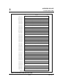
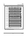
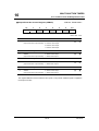
Table 1.3.1 Description of the 32171 Pin Function (2/5)
Type
Pin Name Signal Name
Input/Output Function
Data
DB0-DB15 Data bus
Input/output These pins comprise 16-bit data bus to connect external devices. In write
bus
cycles, the valid byte positions to be written on the 16-bit data bus are
output as BHW/BHE and BLW/BLE. In read cycles, data is always read
from the 16-bit data bus. However, when transferring to the internal circuit
of the M32R, only data at the valid byte positions are transferred.
___
Bus
CS0,
control
CS1
Chip select
Output
These pins comprise external device chip select signal. For
___
areas for which a chip select signal is output, refer to
Chapter 3, "Address Space."
__
RD
Read
Output
This signal is output when reading an external device.
Output
Indicates the byte position to which valid data is transferred
___ ___
BHW/BHE Byte high
___ ___
write/enable
when writing to an external device. BHW/BHE corresponds
___ ___
___ ___
BLW/BLE Byte low
Output
write/enable
to the upper address (D0-D7 is valid); BLW/BLE
corresponds to the lower address (D8-D15 is valid).
____
WAIT
Wait
Input
When the M32R accesses an external device, a low on this
____
WAIT input extends the wait cycle.
____
HREQ
Hold request
Input
This pin is used by an external device to request control of
____
the external bus. A low on this HREQ input causes the
M32R to enter a hold state.
____
HACK
Hold
Output
acknowledge
Multijunction
timer
A-D
This signal is used to notify that the M32R has entered a
hold state and relinquished control of the external bus.
TIN 0,TIN 3
TIN 16–TIN 23 Timer input
Input
Input pins for multijunction timer.
TO 0– TO 20 Timer output
Output
Output pins for the multijunction timer.
TCLK 0– TCLK 3 Timer clock
Input
Clock input pins for the multijunction timer.
AVCC0
Analog power supply
—
converter
AVCC0 is the power supply for the A-D0 converter.
Connect AVCC0 to the power supply rail.
AVSS0
Analog ground
—
AVSS0 is analog ground for the A-D0 converter.
—
Connect AVSS0 to the ground.
1-12
Ver.0.10
OVERVIEW
1
1.3 Pin Function
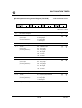
Table 1.3.1 Description of the 32171 Pin Function (3/5)
Type
Pin Name Signal Name
Input/Output Function
A-D
AD0IN0
Analog input
Input
16-channel analog input pins for the A-D0 converter.
voltage input
Input
VREF0 is the reference voltage input pin for the A-D1 converter.
converter – AD0IN15
VREF0
___
Interrupt
System break Input
System break interrupt (SBI) input pin for the interrupt
controller
SBI
interrupt
controller
Serial I/O SCLKI0 /
UART transmit/ Input/output
When channel 0 is in UART mode:
SCLKO0
This pin outputs a clock derived from BRG output by halving it.
receive clock
output or CSIO
transmit/receive
When channel 0 is in CSIO mode:
clock input/output
This pin accepts as its input a transmit/receive clock when external clock
source is selected or outputs a transmit/receive clock when internal clock
source is selected.
SCLKI1 /
UART transmit/ Input/output
SCLKO1
receive clock
When channel 1 is in UART mode:
This pin outputs a clock derived from BRG output by halving it.
output or CSIO
transmit/receive
When channel 1 is in CSIO mode:
clock input/output
This pin accepts as its input a transmit/receive clock when external clock
source is selected or outputs a transmit/receive clock when internal clock
source is selected.
Real-time
debugger
TXD0
Transmit data output
Transmit data output pin for serial I/O channel 0
RXD0
Receive data
Receive data input pin for serial I/O channel 0
TXD1
Transmit data Output
Transmit data output pin for serial I/O channel 1.
RXD1
Receive data
Receive data input pin for serial I/O channel 1.
TXD2
Transmit data Output
Transmit data output pin for serial I/O channel 2.
RXD2
Receive data
Receive data input pin for serial I/O channel 2.
RTDTXD
Transmit data Output
Serial data output pin for the real-time debugger.
RTDRXD
Receive data
Input
Serial data input pin for the real-time debugger.
RTDCLK
Clock input
Input
Input
Input
Input
Serial data transmit/receive clock input pin for the
real-time debugger.
RTDACK
Acknowledge
Output
This pin outputs a low pulse synchronously with the beginning
clock of the real-time debugger's serial data output word. The
duration of this low pulse indicates the type of command/data
that the real-time debugger has received.
Flash
-only
FP
Flash Protect
Input
This mode pin has a function to protect the flash
memory against E/W in hardware.
1-13
Ver.0.10
OVERVIEW
1
1.3 Pin Function
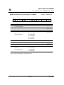
Table 1.3.1 Description of the 32171 Pin Function (4/5)
Type
Pin Name Signal Name
Input/Output Function
CAN
CTX
Data output
Output
This pin outputs data from the CAN module.
CRX
Data input
Input
This pin is used to input data to the CAN module.
JTMS
Test mode
Input
Test mode select input to control state transition of the
JTAG
test circuit.
JTCK
clock
Input
Clock input for the debug module and test circuit.
JTRST
Test reset
Input
Test reset input to initialize the test circuit
asynchronously.
JTDI
Serial input
Input
This pin is used to input test instruction code or test
data serially.
JTDO
Serial output
Output
This pin outputs test instruction code or test data
serially.
Input/
output
port
(Note)
P00 – P07 Input/output
Input/output
Programmable input/output port.
Input/output
Programmable input/output port.
Input/output
Programmable input/output port.
Input/output
Programmable input/output port.
Input/output
Programmable input/output port.
Input/output
Programmable input/output port.
port 0
P10 – P17 Input/output
port 1
P20 – P27 Input/output
port 2
P30 – P37 Input/output
port 3
P41 – P47 Input/output
port 4
P61 – P64 Input/output
port 6
P70 – P77 Input/output
(However, P64 is an input-only port.)
Input/output
Programmable input/output port.
Input/output
Programmable input/output port.
Input/output
Programmable input/output port.
Input/output
Programmable input/output port.
Input/output
Programmable input/output port.
port 7
P82 – P87 Input/output
port 8
P93 – P97 Input/output
port 9
P100
Input/output
– P107
port 10
P110
Input/output
– P117
port 11
Note: Input/output port 5 is reserved for future use.
1-14
Ver.0.10
OVERVIEW
1
1.3 Pin Function
Table 1.3.1 Description of the 32171 Pin Function (5/5)
Type
Pin Name Signal Name
Input/Output Function
Input/
output
port
P124
Input/output
Input/output
Programmable input/output port.
– P127
port 12
(Note1)
P130
Input/output
Input/output
Programmable input/output port.
– P137
port 13
P150,
Input/output
Input/output
Programmable input/output port.
P153
port 15
Input/output
Programmable input/output port.
Input/output
Programmable input/output port.
P174,
Input/output
P175
port 17
P220,P221 Input/output
P225(Note2) port 22
(However, P221 is an input only port.)
Note 1: For the 32171, input/output ports 14, 16, 18, 19, 20, and 21 are nonexistent.
Note 2: Use caution when using P225 because they have a debug event function.
1-15
Ver.0.10
OVERVIEW
1
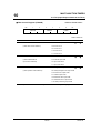
1.4 Pin Layout
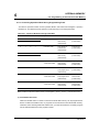
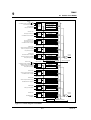
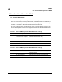
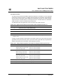
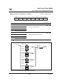
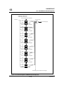
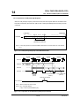
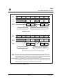
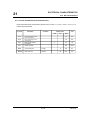
1.4 Pin Layout
Figure 1.4.1 shows pin assignments on the M32171FxVFP. Table 1.4.1 lists the pin
P64/ SBI
P63
P62
P61
FVCC
108
107
106
105
104
103
102
101
100
99
98
97
96
95
94
93
92
91
90
89
88
87
86
85
84
83
82
81
80
79
78
77
76
75
74
73
VDD
P102/TO10
P101/TO9
P100/TO8
P117/TO7
P116/TO6
P115/TO5
P114/TO4
P113/TO3
P112/TO2
P111/TO1
P110/TO0
VSS
VCCE
FP
MOD1
MOD0
RESET
P97/TO20
P96/TO19
P95/TO18
P94/TO17
P93/TO16
P77/RTDCLK
P76/RTDACK
P75/RTDRXD
P74/RTDTXD
P73/ HACK
P72/ HREQ
P71/ WAIT
P70/BCLK / WR
assignments.
109
110
111
112
113
114
115
116
117
118
119
120
121
122
123
124
125
126
127
128
129
130
131
132
133
134
135
136
137
138
139
140
141
142
143
144
M32171FxVFP
72
71
70
69
68
67
66
65
64
63
62
61
60
59
58
57
56
55
54
53
52
51
50
49
48
47
46
45
44
43
42
41
40
39
38
37
VSS
P87/SCLKI1/SCLKO1
P86/RXD1
P85/TXD1
P84/SCLKI0/SCLKO0
P83/RXD0
P82/TXD0
VCCE
P175/RXD2
P174/TXD2
VSS
VCCI
AVSS0
AD0IN15
AD0IN14
AD0IN13
AD0IN12
AD0IN11
AD0IN10
AD0IN9
AD0IN8
AD0IN7
AD0IN6
AD0IN5
AD0IN4
AD0IN3
AD0IN2
AD0IN1
AD0IN0
AVCC0
VREF0
P17/DB15
P16/DB14
P15/DB13
P14/DB12
P13/DB11
P24/A27
P25/A28
P26/A29
P27/A30
P00/DB0
P01/DB1
P02/DB2
P03/DB3
P04/DB4
P05/DB5
P06/DB6
P07/DB7
P10/DB8
P11/DB9
P12/DB10
(Note)
P221/CRX
P225/A12
OSC-VSS
XIN
XOUT
OSC-VCC
VCNT
P30/A15
P31/A16
P32/A17
P33/A18
P34/A19
P35/A20
P36/A21
P37/A22
P20/A23
P21/A24
P22/A25
P23/A26
VCCE
VSS
1
2
3
4
5
6
7
8
9
10
11
12
13
14
15
16
17
18
19
20
21
22
23
24
25
26
27
28
29
30
31
32
33
34
35
36
JTMS
JTCK
JTRST
JTDO
JTDI
P103/TO11
P104/TO12
P105/TO13
P106/TO14
P107/TO15
P124/TCLK0
P125/TCLK1
P126/TCLK2
P127/TCLK3
VCCI
P130/TIN16
P131/TIN17
P132/TIN18
P133/TIN19
P134/TIN20
P135/TIN21
P136/TIN22
P137/TIN23
VCCE
P150/TIN0
P153/TIN3
P41/ BLW / BLE
P42/ BHW / BHE
VCCI
VSS
P43/ RD
P44/ CS0
P45/ CS1
P46/A13
P47/A14
P220/CTX
Package: 144P6Q (0.5 mm pitch)
Note: Use caution when using these pins because they have a debug event function.
Figure 1.4.1 Pin Layout Diagram of the M32171FxVFP (Top View)
1-16
Ver.0.10
OVERVIEW
1
1.4 Pin Layout
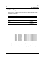
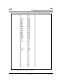
Table 1.4.1 Pin Assignments of the M32171FxVFP
No.
Pin Name
No.
Pin Name
No.
Pin Name
No.
Pin Name
1
P221/CRX
2
P225/A12
41
P17 / DB15
81
P73/HACK
121
P126 / TCLK2
42
VREF0
82
P74 / RTDTXD
122
3
OSC-VSS
43
P127 / TCLK3
AVCC0
83
P75 / RTDRXD
123
VCCI
4
XIN
44
5
XOUT
45
AD0IN0
84
P76 / RTDACK
124
P130 / TIN16
AD0IN1
85
P77 / RTDCLK
125
P131 / TIN17
6
OSC-VCC
46
7
VCNT
47
AD0IN2
86
P93 / TO16
126
P132 / TIN18
AD0IN3
87
P94 / TO17
127
8
P30 / A15
P133 / TIN19
48
AD0IN4
88
P95 / TO18
128
9
P134 / TIN20
P31 / A16
49
AD0IN5
89
P96 / TO19
129
P135 / TIN21
10
P32 / A17
50
AD0IN6
90
P97 / TIN20
130
P136 / TIN22
11
P33 / A18
51
AD0IN7
91
RESET
131
P137 / TIN23
12
P34 / A19
52
AD0IN8
92
MOD0
132
VCCE
13
P35 / A20
53
AD0IN9
93
MOD1
133
P150 / TIN0
14
P36 / A21
54
AD0IN10
94
FP
134
P153 / TIN3
15
P37 / A22
55
AD0IN11
95
VCCE
135
P41 / BLW / BLE
16
P20 / A23
56
AD0IN12
96
VSS
136
P42 / BHW / BHE
17
P21 / A24
57
AD0IN13
97
P110 / TO0
137
VCCI
18
P22 / A25
58
AD0IN14
98
P111 / TO1
138
VSS
19
P23 / A26
59
AD0IN15
99
P112 / TO2
139
P43 / RD
20
VCCE
60
AVSS0
100
P113 / TO3
140
P44 / CS0
21
VSS
61
VCCI
101
P114 / TO4
141
P45 / CS1
22
P24 / A27
62
VSS
102
P115 / TO5
142
P46 / A13
23
P25 / A28
63
P174 / TXD2
103
P116 / TO6
143
P47 / A14
24
P26 / A29
64
P175 / RXD2
104
P117 / TO7
144
P220 / CTX
25
P27 / A30
65
VCCE
105
P100 / TO8
26
P00 / DB0
66
P82 / TXD0
106
P101/ TO9
27
P01 / DB1
67
P83 / RXD0
107
P102 / TO10
28
P02 / DB2
68
P84 / SCLKI0 / SCLKO0
108
VDD
29
P03 / DB3
69
P85 / TXD1
109
JTMS
30
P04 / DB4
70
P86 / RXD1
110
JTCK
31
P05 / DB5
71
P87 / SCLKI1 / SCLKO1
111
JTRST
32
P06 / DB6
72
VSS
112
JTDO
33
P07 / DB7
73
FVCC
113
JTDI
34
P10 / DB8
74
P61
114
P103 / TO11
35
P11 / DB9
75
P62
115
P104 / TO12
36
P12 / DB10
76
P63
116
P105 / TO13
37
P13 / DB11
77
P64 / SBI
117
P106 / TO14
38
P14 / DB12
78
P70/ BCLK / WR
118
P107 / TO15
39
P15 / DB13
79
P71 / WAIT
119
P124 / TCLK0
40
P16 / DB14
80
P72 / HREQ
120
P125 / TCLK1
1-17
Ver.0.10
1
❊ This is a blank page. ❊
1-18
Ver.0.10
CHAPTER 2
CPU
2.1
2.2
2.3
2.4
2.5
2.6
CPU Registers
General-purpose Registers
Control Registers
Accumulator
Program Counter
Data Formats
CPU
2
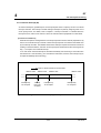
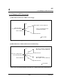
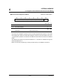
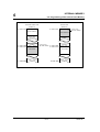
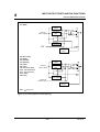
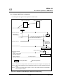
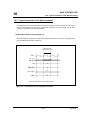
2.1 CPU Registers
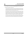
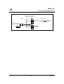
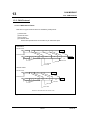
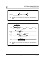
2.1 CPU Registers
The M32R has sixteen general-purpose registers, five control registers, an accumulator, and a
program counter. The accumulator is a 56-bit configuration, and all other registers are a 32-bit
configuration.
2.2 General-purpose Registers
General-purpose registers are 32 bits in width and there are sixteen of them (R0 to R15), which are
used to hold data and base addresses. Especially, R14 is used as a link register, and R15 is used
as a stack pointer. The link register is used to store the return address when executing a subroutine
call instruction. The stack pointer is switched between an interrupt stack pointer (SPI) and a user
stack pointer (SPU) depending on the value of the Processor Status Word register (PSW)'s stack
mode (SM) bit.
0
0
31
R0
R1
R2
R3
R4
R5
R6
R7
31
R8
R9
R10
R11
R12
R13
R14 (Link register)
R15 (Stack pointer)
(Note)
Note: The stack pointer is switched between an interrupt stack pointer (SPI) and a user stack pointer
(SPU) depending on the value of the PSW's SM bit.
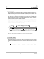
Figure 2.2.1 General-purpose Registers
2-2
Ver.0.10
CPU
2
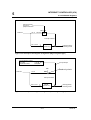
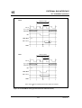
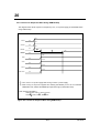
2.3 Control Registers
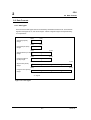
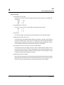
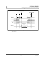
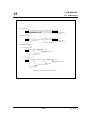
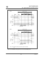
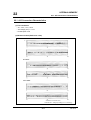
2.3 Control Registers
There are five control registers-Processor Status Word Register (PSW), Condition Bit Register
(CBR), Interrupt Stack Pointer (SPI), User Stack Pointer (SPU), and Backup PC (BPC).
Dedicated "MVTC" and "MVFC" instructions are used to set and read these control registers.
CRn
Control Registers
0
31
CR0
CR1
CR2
CR3
PSW
CBR
SPI
SPU
Processor status Word Register
Condition Bit Register
Interrupt Stack Pointer
User Stack Pointer
CR6
BPC
Backup PC
Notes 1: CRn (n = 0-3, 6) denotes control register numbers.
2: Dedicated "MVTC" and "MVFC" instructions are used to set and read the control registers.
Figure 2.3.1 Control Registers
2-3
Ver.0.10
CPU
2
2.3 Control Registers
2.3.1 Processor Status Word Register: PSW (CR0)
The Processor Status Word Register (PSW) is used to indicate the status of the M32R. It consists
of a regularly used PSW field and a special BPSW field which is used to save the PSW field when
an EIT occurs.
The PSW field consists of several bits labeled Stack Mode (SM), Interrupt Enable (IE), and
Condition bit (C). The BPSW field consists of backup bits of the foregoing, i.e., Backup SM bit
(BSM), Backup IE bit (BIE), and Backup C bit (BC).
BPSW field
0(MSB)
PSW
7
8
PSW field
15 16 17
0 0 0 0 0 0 0 0 0 0 0 0 0 0 0 0
BSM
31(LSB)
23 24 25
0 0 0 0 0
BIE
BC
0 0 0 0 0
SM
IE
C
(Note 1)
D
Bit Name
Function
Initial
16
BSM (Backup SM)
Holds the value of SM bit when EIT
R
W
Indeterminate
is accepted.
17
BIE (Backup IE)
Holds the value of IE bit when EIT
Indeterminate
is accepted.
23
BC (Backup C)
Holds the value of C bit when EIT
Indeterminate
is accepted.
24
SM (Stack Mode)
0: Interrupt stack pointer is used.
0
1: User stack pointer is used.
25
IE (Interrupt Enable)
0: No interrupt is accepted.
0
1: Interrupt is accepted.
31
C (Condition bit)
Depending on instruction execution, it indicates
0
whether operation resulted in a carry, borrow, or overflow.
Notes 1: "Initial" shows the state immediately after reset, R = O means the register is readable, W = O
means the register is writable.
2: For changes of the state of each bit when an EIT event occurs, refer to Chapter 4, "EIT.”
2-4
Ver.0.10
CPU
2
2.3 Control Registers
2.3.2 Condition Bit Register: CBR (CR1)
The Condition Bit Register (CBR) is created as a separate register from the PSW by extracting the
Condition bit (C) from it. The value written to the PSW C bit is reflected in this register. This register
is a read-only register (writes to this register by "MVTC" instruction are ignored).
0(MSB)
31(LSB)
CBR 0 0 0 0 0 0 0 0 0 0 0 0 0 0 0 0 0 0 0 0 0 0 0 0 0 0 0 0 0 0 0 C
2.3.3 Interrupt Stack Pointer: SPI (CR2)
User Stack Pointer: SPU (CR3)
The Interrupt Stack Pointer (SPI) and User Stack Pointer (SPU) hold the current address of the
stack pointer. These registers can be accessed as general-purpose register R15. In this case,
whether R15 is used as SPI or as SPU depends on the PSW's Stack Mode (SM) bit.
0(MSB)
31(LSB)
SPI
SPI
0(MSB)
31(LSB)
SPU
SPU
2.3.4 Backup PC: BPC (CR6)
The Backup PC (BPC) is a register used to save the value of the Program Counter (PC) when an
EIT occurs. Bit 31 is fixed to 0.
When an EIT occurs, the value held in the PC immediately before the EIT occurred or the value of
the next instruction is set in this register. When the "RTE" instruction is executed, the saved value
is returned from the BPC to the PC. However, the two low-order bits of the PC when thus returned
are always fixed to "00" (control always returns to word boundaries.)
0(MSB)
31(LSB)
BPC
BPC
2-5
0
Ver.0.10
CPU
2
2.4 Accumulator
2.4 Accumulator
The accumulator (ACC) is a 56-bit register used by DSP function instructions. When read out or
written to, it is handled as a 64-bit register. When reading, the value of bit 8 is sign-extended. When
writing, bits 0--7 are ignored. Also, the accumulator is used by the multiplication instruction "MUL."
Note that when executing this instruction, the value of the accumulator is destroyed.
The "MVTACHI" and "MVTACLO" instructions are used to write to the accumulator. The
"MVTACHI" instruction writes data to the 32 high-order bits (bits 0-31), and the "MVTACLO"
instruction writes data to the 32 low-order bits (bits 32-63).
The "MVFACHI," "MVFACLO," and "MVFACMI" instructions are used to read data from the
accumulator. The "MVFACHI" instruction reads data from the 32 high-order bits (bits 0-31), the
"MVFACLO" instruction reads data from the 32 low-order bits (bits 32-63), and the "MVFACHI"
instruction reads data from the 32 middle bits (bits 16-47).
Range of bits read by MVFACMI
instruction
(Note)
0(MSB)
78
15 16
31 32
47 48
63(LSB)
ACC
Range of bits read/written to by
MVFACHI/MVTACHI instructions
Range of bits read/written to by
MVFACLO/MVTACLO instructions
Note: Bits 0-7 always show the sign-extended value of bit 8. Writes to this bit field are ignored.
2.5 Program Counter
The Program Counter (PC) is a 32-bit counter used to hold the address of the currently executed
instruction. Because M32R instructions each start from an even address, the LSB (bit 31) is always
0.
0(MSB)
31(LSB)
PC
PC
2-6
0
Ver.0.10
CPU
2
2.6 Data Formats
2.6 Data Formats
2.6.1 Data Types
There are several data types that can be handled by the M32R's instruction set. These include
signed and unsigned 8, 16, and 32-bit integers. Values of signed integers are represented by
2's complements.
0(MSB)
Signed byte (8-bit)
integer
7(LSB)
S
0(MSB)
7(LSB)
Unsigned byte (8-bit)
integer
15(LSB)
0(MSB)
Signed halfword (16-bit)
S
integer
15(LSB)
0(MSB)
Unsigned halfword
(16-bit) integer
31(LSB)
0(MSB)
Signed word (32-bit)
integer
S
31(LSB)
0(MSB)
Unsigned word (32-bit)
integer
S : Sign bit
Figure 2.6.1 Data Types
2-7
Ver.0.10
CPU
2
2.6 Data Formats
2.6.2 Data Formats
(1) Data formats in register
Data sizes in M32R registers are always words (32 bits).
When loading byte (8-bit) or halfword (16-bit) data from memory into a register, the data is signextended (LDB, LDH instructions) or zero-extended (LDUB, LDUH instructions) into word (32-bit)
data before being stored in the register. When storing data from M32R register into memory, the
register data is stored in memory in different sizes depending on the instructions used. The ST
instruction stores the entire 32-bit data of the register, the STH instruction stores the least
significant 16-bit data, and the STB instruction stores the least significant 8-bit data.
<When loading>
0(MSB)
Sign-extended (LDB instruction) or
zero-extended (LDUB instruction)
From memory (LDB,
LDUB instructions)
24
Rn
31(LSB)
Byte
Sign-extended (LDH instruction) or
zero-extended (LDUH instruction)
From memory (LDH, LDUH instructions)
16
0(MSB)
31(LSB)
Halfword
Rn
From memory (LD instructions)
0(MSB)
31(LSB)
Word
Rn
<When storing>
0(MSB)
24
31(LSB)
Byte
Rn
To memory (STB instruction)
16
0(MSB)
31(LSB)
Halfword
Rn
To memory (STH instruction)
0(MSB)
31(LSB)
Rn
Word
To memory (ST instruction)
Figure 2.6.2 Data Formats in Register
2-8
Ver.0.10
CPU
2
2.6 Data Formats
(2) Data formats in memory
Data sizes in memory are either byte (8 bits), halfword (16 bits), or word (32 bits). Byte data can
be located at any address. However, halfword data must be located at halfword boundaries
(where the LSB address bit = "0"), and word data must be located at word boundaries (where two
LSB address bits = "00"). If an attempt is made to access memory data across these halfword or
word boundaries, an address exception is generated.
Address
+ 0 address
0
+ 1 address
7 8
+ 2 address
15 16
+ 3 address
23 24
31
Byte
Byte
Byte
Byte
Byte
(MSB)
(LSB)
Halfword
Halfword
Halfword
(MSB)
(LSB)
Word
Word
Figure 2.6.3 Data Formats in Memory
2-9
Ver.0.10
CPU
2
2.6 Data Formats
(3) Endian
The following shows the generally used endian methods and the M32R family endian.
Bit endian
(H'01)
MSB
Byte endian
(H'01234567)
LSB
MSB
B'0000001
Big endian
D0
D7
MSB
LSB
D7
H'23
H'45
H'67
HH
HL
LH
LL
MSB
B'0000001
Little endian
LSB
H'01
D0
LSB
H'67
H'45
H'23
H'01
LL
LH
HL
HH
Note: Even for bit big endian, H'01 is not B'10000000.
Figure 2.6.4 Endian Methods
7700 family
M16C family
MPU name
Endian
(Bit/Byte)
Address
Little/Little
+0
+1
+2
MSB
Data
arrangement
Bit number
Ex:0x01234567
+3
LSB
LL
LH
31-24
23-16
HL
15-8
HH
7-0
+0
Competition
M32R family
M16 family
Little/Big
Big/Big
+1
+2
+3
MSB
LSB
HH
HL
31-24
23-16
.byte 67,45,23,01
LH
15-8
LL
7-0
.byte 01,23,45,67
+0
+1
+2
+3
HL
LH
LL
MSB
HH
0-7
LSB
8-15
16-23
24-31
.byte 01,23,45,67
Note: The M32R's endian method is big endian for both bit and byte.
Figure 2.6.5 M32R Family Endian
2-10
Ver.0.10
CPU
2
2.6 Data Formats
(4) Transfer instructions
• Constant transfer
LD24
Rdest, #imm24
imm24
LD24
Rdest, #imm24
LDI
Rdest, #imm16
LDI
Rdest, #imm8
0
23
Rdest
00
0
8
31
SETH Rdest, #imm16
SETH Rdest, #imm16
imm16
0
15
Rdest
00
0
00
31
15
• Register to register transfer
MV
MV
Rdest, Rsrc
Rdest, Rsrc
Rsrc
0
31
Rdest
0
31
• Control register transfer
MVTC Rsrc, CRdest
MVFC Rdest, CRsrc
Rsrc
MVTC Rsrc, CRdest
0
31
CRdest
0
31
Note: For the MVTC instruction, the condition bit C does not change unless CRdest is CR0 (PSW).
Figure 2.6.6 Transfer instructions
2-11
Ver.0.10
CPU
2
2.6 Data Formats
(5) Memory (signed) to register transfer
Memory
Register
• Signed 32 bits
LD24
LD
Rsrc, #label
Rdest, @Rsrc
label
Rdest
+0
+1
+2
+3
+0
+1
+2
+3
0
31
• Signed 16 bits
label
LD24
LDH
Rdest
Rsrc, #label
Rdest, @Rsrc
Check the MSB
0 = positive
1 = negative
00
00
FF
FF
0
31
• Signed 8 bits
label
LD24
LDB
Rdest
Rsrc, #label
Rdest, @Rsrc
+0
+1
+2
+3
Check the MSB
0 = positive
1 = negative
00
00
00
FF
FF
FF
0
31
Figure 2.6.7 Memory (signed) to register transfer
(6) Memory (unsigned) to register transfer
Memory
• Unsigned 32 bits
LD24
LD
Rsrc, #label
Rdest, @Rsrc
Register
Rdest
label
+0
+1
+2
+3
0
31
• Unsigned 16 bits
label
Rdest
LD24 Rsrc, #label
LDUH Rdest, @Rsrc
00
+0
+1
+2
+3
00
0
31
• Unsigned 8 bits
label
Rdest
LD24 Rsrc, #label
LDUB Rdest, @Rsrc
00
+0
+1
+2
+3
0
00
00
31
Figure 2.6.8 Memory (unsigned) to register transfer
2-12
Ver.0.10
CPU
2
2.6 Data Formats
(7) Things to be noted for data transfer
Note that in data transfer, data arrangements in registers and those in memory are different.
Data in memory
Data in register
(R0-R15)
Word data (32 bits)
HH
HL
LH
LL
D0
D31
MSB
LSB
(R0-R15)
Half-word data (16 bits)
H
+0
+1
+2
+3
HH
HL
LH
LL
D0
D0
D31
LSB
(R0-R15)
LSB
+0
+1
H
L
L
MSB
D31
MSB
D0
+2
+3
+2
+3
D15
MSB
+0
LSB
+1
Byte data (8 bits)
D0
D31
MSB
LSB
D0
D7
MSB LSB
Figure 2.6.9 Difference in Data Arrangements
2-13
Ver.0.10
2
❊ This is a blank page. ❊
2-14
Ver.0.10
CHAPTER 3
ADDRESS SPACE
3.1 Outline of Address Space
3.2 Operation Modes
3.3 Internal ROM Area and Extended
External Area
3.4 Internal RAM Area and SFR Area
3.5 EIT Vector Entry
3.6 ICU Vector Table
3.7 Note about Address Space
ADDRESS SPACE
3
3.1 Outline of Address Space
3.1 Outline of Address Space
The M32R's logical addresses are always handled in 32 bits, providing 4 Gbytes of linear address space. The M32R/E's address space consists of the following:
(1) User space
• Internal ROM area
• Extended external area
• Internal RAM area
• Special Function Register (SFR) area
(2) Boot program space
(3) System space (areas not open to the user)
(1) User space
A 2 Gbytes of address space from H'0000 0000 to H'7FFF FFFF is the user space. Located in
this space are the internal ROM area, extended external area, internal RAM area, and Special Function Register (SFR) area, an area containing a group of internal peripheral I/O registers. Of these, the internal ROM and extended external areas are located differently depending on mode settings which will be described later.
(2) Boot program space
A 1 Gbyte of address space from H'8000 0000 to H'BFFF FFFF is the boot program space.
This space stores a program (boot program) which enables on-board programming when the
internal flash area is blank.
(3) System space
A 1 Gbyte of address space from H'C000 0000 to H'FFFF FFFF is the system space. This
space is reserved for use by development tools such as an in-circuit emulator or a debug
monitor, and cannot be used by the user.
3-2
Ver.0.10
ADDRESS SPACE
3
3.1 Outline of Address Space
<Logical address space of M32171F4>
Extended external
area
(4 Mbytes)
EIT vector entry
Logical address
H'0000 0000
H'0000 0000
Internal ROM area
(Note 1)
(16 Mbytes)
H'0007 FFFF
Reserved area
(512 Kbytes)
2 Gbytes
Ghost area
in units of
16 Mbytes
H'001F FFFF
CS1 area
(1 Mbyte)
Ghost area in
CS1
(1 Mbyte)
BOOT ROM area
(8 Kbytes)
Reserved area
(8 Kbytes)
H'8000 0000
H'8000 1FFF
H'8000 2000
H'007F FFFF
SFR area
(16 Kbytes)
Ghost area
in units of
16 Mbytes
H'002F FFFF
H'0030 0000
Ghost area in
4 Mbytes
H'8000 3FFF
H'8000 4000
Boot
program
space
(Note 2)
H'0020 0000
H'003F FFFF
H'0040 0000
H'7FFF FFFF
1 Gbyte
H'000F FFFF
H'0010 0000
CS0 area
(1 Mbyte)
User space
H'8000 0000
H'0008 0000
H'0080 0000
H'0080 3FFF
H'0080 4000
Internal RAM area
(16 Kbytes)
H'0080 7FFF
H'0080 8000
Reserved area
(96 Kbytes)
H'BFFF FFFF
H'BFFF FFFF
H'C000 0000
1 Gbyte
H'0081 FFFF
H'0082 0000
Ghost area in
units of 128
Kbytes
System space
H'FFFF FFFF
H'00FF FFFF
Notes1: This location varies with chip mode settings.
2: The boot program space can read out only when FP = 1, MOD0 = 1, and MOD1 = 0.
Figure 3.1.1 Address Space of the M32171F4
3-3
Ver.0.10
ADDRESS SPACE
3
3.1 Outline of Address Space
<Logical address space of M32171F3>
Extended external
area
(4 Mbytes)
EIT vector entry
Logical address
H'0000 0000
H'0000 0000
Internal ROM area
(Note 1)
(16 Mbytes)
Reserved area
(640 Kbytes)
2 Gbytes
H'0005 FFFF
H'0006 0000
H'000F FFFF
H'0010 0000
CS0 area
(1 Mbyte)
User space
Ghost area
in units of
16 Mbytes
H'001F FFFF
H'0020 0000
CS1 area
(1 Mbyte)
H'002F FFFF
H'0030 0000
Ghost area in
CS1
(1 Mbyte)
H'7FFF FFFF
H'8000 0000
BOOT ROM area
(8 Kbytes)
Reserved area
(8 Kbytes)
1 Gbyte
H'8000 0000
H'8000 1FFF
H'8000 2000
Ghost area in
4 Mbytes
H'8000 3FFF
H'8000 4000
H'007F FFFF
SFR area
(16 Kbytes)
Boot
program
space
(Note 2)
H'003F FFFF
H'0040 0000
Ghost area
in units of
16 Mbytes
H'0080 0000
H'0080 3FFF
H'0080 4000
Internal RAM area
(16 Kbytes)
H'0080 7FFF
H'0080 8000
Reserved area
(96 Kbytes)
H'BFFF FFFF
H'BFFF FFFF
H'C000 0000
1 Gbyte
H'0081 FFFF
H'0080 8000
Ghost area in
units of 128
Kbytes
System space
H'FFFF FFFF
H'00FF FFFF
Notes1: This location varies with chip mode settings.
2: The boot program space can read out only when FP = 1, MOD0 = 1, and MOD1 = 0.
Figure 3.1.2 Address Space of the M32171F3
3-4
Ver.0.10
ADDRESS SPACE
3
3.2 Operation Modes
3.2 Operation Modes
The 32171 is placed in one of the following modes by setting its operation mode (using MOD0 and
MOD1 pins). For details about the mode used to rewrite the internal flash memory, refer to Section
6.5, "Programming of Internal Flash Memory."
Table 3.2.1 Setting Operation Modes
MOD0
MOD1 (Note 1)
Operation Mode (Note 2)
VSS
VSS
Single-chip mode
VSS
VCC
Extended external mode
VCC
VSS
Processor mode (FP = VSS)
VCC
VCC
Reserved (cannot be used)
Notes 1: VCC connects to +5 V, and VSS connects to GND.
2: For flash rewrite mode (FP = VCC) not listed in the above table, refer to Section 6.5, "Programming
of Internal Flash Memory."
The internal ROM and extended external areas are located differently depending on the 32171's
operation mode. (All other areas in address space are located the same way.) The address maps of
internal ROM and extended external areas in each mode are shown below. (For flash rewrite mode
(FP = VCC) not listed in the above table, refer to Section 6.5, "Programming of Internal Flash
Memory.")
Non-CS0 area
H'0000 0000
Internal ROM
area
(512 Kbytes)
CS0 area
(1 Mbytes)
Reserved area
(512 Kbytes)
H'000F FFFF
H'0010 0000
CS0 area
(1 Mbyte)
Extended external area
H'001F FFFF
H'0020 0000
H'002F FFFF
H'0020 0000
CS1 area
(1 Mbytes)
Ghost area in
CS1
(1 Mbyte)
Extended external area
H'0007 FFFF
H'0008 0000
Internal ROM
area
(512 Kbytes)
Ghost area in
CS0
(1 Mbyte)
CS1 area
(1 Mbytes)
Ghost area in
CS1
(1 Mbyte)
H'003F FFFF
<Single-chip mode>
<Extended external mode>
<Processor mode>
Figure 3.2.1 M32171F4 Operation Mode and Internal ROM/Extended External Areas
3-5
Ver.0.10
ADDRESS SPACE
3
3.2 Operation Modes
Non-CS0 area
H'0000 0000
Internal ROM
area
(384 Kbytes)
CS0 area
(1 Mbytes)
Reserved area
(640 Kbytes)
H'000F FFFF
H'0010 0000
CS0 area
(1 Mbyte)
Extended external area
H'001F FFFF
H'0020 0000
H'002F FFFF
H'0030 0000
CS1 area
(1 Mbytes)
Ghost area in
CS1 (1 Mbytes)
Extended external area
H'0005 FFFF
H'0006 0000
Internal ROM
area
(384 Kbytes)
Ghost area in
CS0
(1 Mbytes)
CS1 area
(1 Mbytes)
Ghost area in
CS1
(1 Mbytes)
H'003F FFFF
<Single-chip mode>
<Extended external mode>
<Processor mode>
Figure 3.2.2 M32171F3 Operation Mode and Internal ROM/Extended External Areas
3-6
Ver.0.10
ADDRESS SPACE
3
3.3 Internal ROM/Extended External Area
3.3 Internal ROM Area and Extended External Area
The 8 Mbyte area at addresses H'0000 0000 to H'007F FFFF in the user space accommodates the
internal ROM and extended external areas. Of this, a 4 Mbytes of address space from H'0000 0000
to H'0003 FFFF is the area that the user can actually use. All other areas here comprise a 4 Mbytes
of ghost area. (When programming, do not use this ghost area intentionally.)
For details on how the internal ROM and extended external areas are located differently depending
on the 32171's operation modes set, refer to Section 3.2, "Operation Modes."
3.3.1 Internal ROM Area
The internal ROM is located in the area shown below. Also, this area has an EIT vector entry
(and ICU vector table) located in it at the beginning.
Table 3.3.1 Addresses at Which the 32171's Internal ROM is Located
Type Name
Size
Located address
M32171F4
512 Kbytes
H'0000 0000 - H'0007 FFFF
M32171F3
384 Kbytes
H'0000 0000 - H'0005 FFFF
3.3.2 Extended External Area
An extended external area is provided only when extended external mode or processor mode has
been selected when setting the 32171's operation mode. For access to this extended external area,
the 32171 outputs the control signals necessary to access external devices.
________
_______
The 32171's CS0 and CS1 signals are output corresponding to the address mapping of the ex________
_______
tended external area. The CS0 signal is output for the CS0 area, and the CS1 signal is output for
the CS1 area.
Table 3.3.2 Address Mapping of the Extended External Area in Each Operation Mode of the
32171
Operation Mode
Address mapping of the extended external area
Single-chip mode
None
Extended external mode
Addresses H'0010 0000 to H'001F FFFF (CS0 area: 1 Mbytes)
Addresses H'0020 0000 to H'002F FFFF (CS1 area: 1 Mbytes) (Note 1)
Processor mode
Addresses H'0000 0000 to H'000F FFFF (CS0 area: 1 Mbytes) (Note 2)
Addresses H'0020 0000 to H'002F FFFF (CS1 area: 1 Mbytes) (Note 2)
Note 1: During extended external mode, a ghost (1 Mbyte) of the CS1 area appears in an area of
H’0030 0000 through H’003F FFFF.
Note 2: During processor mode, a ghost (1 Mbyte) of the CS0 area appears in an area of H’0010
0000 through H’001F FFFF and a ghost (1 Mbyte) of the CS1 area appears in an area of
H’0030 0000 through H’003F FFFF.
3-7
Ver.0.10
ADDRESS SPACE
3
3.4 Internal ROM/SFR Area
3.4 Internal RAM Area and SFR Area
The 8 Mbyte area at addresses H'0080 0000 to H'00FF FFFF in the user space accommodates the
internal RAM area and Special Function Register (SFR) area. Of this, a 128 Kbytes of address
space from H'0080 0000 to H'0081 FFFF is the area that the user can actually use. All other areas
here comprise a ghost area in units of 128 Kbytes. (When programming, do not use this ghost area
intentionally.)
3.4.1 Internal RAM Area
The internal RAM (16-Kbyte) is allocated to the addresses H’0080 4000 through H’0080 3FFF.
3.4.2 Special Function Register (SFR) Area
Addresses H'0080 0000 to H'0080 3FFFF are the Special Function Register (SFR) area. This area
has registers for internal peripheral I/O located in it.
H'0080 0000
SFR area
(16 Kbytes)
H'0080 3FFF
H'0080 4000
Internal RAM
(16 Kbytes)
Pseudo-flash emulation
areas separated in units of 8
Kbytes or 4 Kbytes can be
allocated here. For details,
refer to Section 6.7.
H'0080 7FFF
Figure 3.4.1 Internal RAM Area and Special Function Register (SFR) Area
3-8
Ver.0.10
ADDRESS SPACE
3
3.4 Internal ROM/SFR Area
0
7 8
+0 address
0
15
7 8
+0 address
+1 address
15
+1 address
H'0080 07E0
H'0080 0000
Flash control
H'0080 07F2
Interrupt
controller (ICU)
H'0080 007E
H'0080 0080
A-D0 converter
H'0080 00EE
H'0080 0100
H'0080 0FE0
MJT (TML1)
Serial I/O0
H'0080 0 FFE
H'0080 0146
Multijunction timer
(MJT)
H'0080 1000
CAN0
H'0080 0180
Wait controller
H'0080 11 FE
H'0080 0200
MJT (common part)
H'0080 023E
H'0080 0240
MJT (TOP)
H'0080 3FFE
H'0080 02FE
H'0080 0300
MJT (TIO)
Multijunction timer
(MJT)
H'0080 03BE
H'0080 03C0
MJT (TMS)
H'0080 03D8
H'0080 03 E0
H'0080 03FE
H'0080 0400
H'0080 0478
MJT (TML0)
DMAC
H'0080 0700
Input/output port
H'0080 0756
H'0080 0760
Note: The Real-time Debugger (RTD) is designed to be an independent module
operated from an external source, and is transparent to the CPU.
Figure 3.4.2 Outline Address Mapping of the SFR Area
3-9
Ver.0.10
ADDRESS SPACE
3
3.4 Internal ROM/SFR Area
Address
+0 Address
+1 Address
D0
D7
H'0080 0000
D8
D15
Interrupt Vector Register (IVECT)
H'0080 0002
H'0080 0004
Interrupt Mask Register (IMASK)
H'0080 0006
SBI Control Register ( SBICR)
~
~
H'0080 0060
~
~
CAN0 Transmit/Receive & Error Interrupt Control Register (ICAN0CR)
H'0080 0062
H'0080 0064
H'0080 0066
H'0080 0068
RTD Interrupt Control Register (IRTDCR)
SIO2,3 Transmit/Receive Interrupt Control Register (ISO23CR)
DMA5-9 Interrupt Control Register (IDMA59CR)
H'0080 006A
H'0080 006C
A-D0 Conversion Interrupt Control Register (IAD0CCR)
H'0080 006E
SIO0 Receive Interrupt Control Register (ISIO0RXCR)
H'0080 0070
SIO1 Receive Interrupt Control Register (ISIO1RXCR)
DMA0-4 Interrupt Control Register (IDMA04CR)
H'0080 0072
MJT Output Interrupt Control Register 0 (IMJTOCR0)
MJT Output Interrupt Control Register 1 (IMJTOCR1)
H'0080 0074
MJT Output Interrupt Control Register 2 (IMJTOCR2)
SIO0 Transmit Interrupt Control Register (ISIO0TXCR)
SIO1 Transmit Interrupt Control Register (ISIO1TXCR)
MJT Output Interrupt Control Register 3 (IMJTOCR3)
H'0080 0076
MJT Output Interrupt Control Register 4 (IMJTOCR4)
MJT Output Interrupt Control Register 5 (IMJTOCR5)
H'0080 0078
MJT Output Interrupt Control Register 6 (IMJTOCR6)
MJT Output Interrupt Control Register 7 (IMJTOCR7)
MJT Input Interrupt Control Register 1 (IMJTICR1)
H'0080 007A
MJT Input Interrupt Control Register 3 (IMJTICR3)
H'0080 007C
MJT Input Interrupt Control Register 2 (IMJTICR2)
H'0080 007E
MJT Input Interrupt Control Register 4 (IMJTICR4)
H'0080 0080
A-D0 Single Mode Register 0 (AD0SIM0)
A-D0 Single Mode Register 1 (AD0SIM1)
A-D0 Scan Mode Register 0 (AD0SCM0)
A-D0 Scan Mode Register 1 (AD0SCM1)
H'0080 0082
H'0080 0084
H'0080 0086
H'0080 0088
A-D0 Successive Approximation Register (AD0SAR)
H'0080 008A
H'0080 008C
A-D0 Comparate Data Register (AD0CMP)
~
~
~
~
H'0080 0090
10-bit A-D0 Data Register 0 (AD0DT0)
H'0080 0092
10-bit A-D0 Data Register 1 (AD0DT1)
H'0080 0094
10-bit A-D0 Data Register 2 (AD0DT2)
H'0080 0096
10-bit A-D0 Data Register 3 (AD0DT3)
H'0080 0098
10-bit A-D0 Data Register 4 (AD0DT4)
H'0080 009A
10-bit A-D0 Data Register 5 (AD0DT5)
H'0080 009C
10-bit A-D0 Data Register 6 (AD0DT6)
H'0080 009E
10-bit A-D0 Data Register 7 (AD0DT7)
H'0080 00A0
10-bit A-D0 Data Register 8 (AD0DT8)
H'0080 00A2
10-bit A-D0 Data Register 9 (AD0DT9)
H'0080 00A4
10-bit A-D0 Data Register 10 (AD0DT10)
H'0080 00A6
10-bit A-D0 Data Register 11 (AD0DT11)
H'0080 00A8
10-bit A-D0 Data Register 12 (AD0DT12)
H'0080 00AA
10-bit A-D0 Data Register 13 (AD0DT13)
H'0080 00AC
10-bit A-D0 Data Register 14 (AD0DT14)
H'0080 00AE
10-bit A-D0 Data Register 15 (AD0DT15)
~
~
~
~
8-bit A-D0 Data Register 0 (AD08DT0)
H'0080 00D0
Blank addresses are reserved areas
Figure 3.4.3 Register Mapping of the SFR Area (1)
3-10
Ver.0.10
ADDRESS SPACE
3
3.4 Internal ROM/SFR Area
Address
+0 Address
+1 Address
D0
D7 D8
H'0080 0000
D15
Interrupt Vector Register (IVECT)
H'0080 0002
H'0080 0004
Interrupt Mask Register (IMASK)
H'0080 0006
SBI Control Register ( SBICR)
~
~
H'0080 0060
~
~
CAN0 Transmit/Receive & Error Interrupt Control Register (ICAN0CR)
H'0080 0062
H'0080 0064
H'0080 0066
H'0080 0068
RTD Interrupt Control Register (IRTDCR)
SIO2,3 Transmit/Receive Interrupt Control Register (ISO23CR)
DMA5-9 Interrupt Control Register (IDMA59CR)
H'0080 006A
H'0080 006C
A-D0 Conversion Interrupt Control Register (IAD0CCR)
H'0080 006E
SIO0 Receive Interrupt Control Register (ISIO0RXCR)
H'0080 0070
SIO1 Receive Interrupt Control Register (ISIO1RXCR)
DMA0-4 Interrupt Control Register (IDMA04CR)
H'0080 0072
MJT Output Interrupt Control Register 0 (IMJTOCR0)
MJT Output Interrupt Control Register 1 (IMJTOCR1)
H'0080 0074
MJT Output Interrupt Control Register 2 (IMJTOCR2)
SIO0 Transmit Interrupt Control Register (ISIO0TXCR)
SIO1 Transmit Interrupt Control Register (ISIO1TXCR)
MJT Output Interrupt Control Register 3 (IMJTOCR3)
H'0080 0076
MJT Output Interrupt Control Register 4 (IMJTOCR4)
MJT Output Interrupt Control Register 5 (IMJTOCR5)
H'0080 0078
MJT Output Interrupt Control Register 6 (IMJTOCR6)
MJT Output Interrupt Control Register 7 (IMJTOCR7)
MJT Input Interrupt Control Register 1 (IMJTICR1)
H'0080 007A
MJT Input Interrupt Control Register 3 (IMJTICR3)
H'0080 007C
MJT Input Interrupt Control Register 2 (IMJTICR2)
H'0080 007E
MJT Input Interrupt Control Register 4 (IMJTICR4)
H'0080 0080
A-D0 Single Mode Register 0 (AD0SIM0)
A-D0 Single Mode Register 1 (AD0SIM1)
A-D0 Scan Mode Register 0 (AD0SCM0)
A-D0 Scan Mode Register 1 (AD0SCM1)
H'0080 0082
H'0080 0084
H'0080 0086
H'0080 0088
A-D0 Successive Approximation Register (AD0SAR)
H'0080 008A
H'0080 008C
A-D0 Comparate Data Register (AD0CMP)
~
~
~
~
H'0080 0090
10-bit A-D0 Data Register 0 (AD0DT0)
H'0080 0092
10-bit A-D0 Data Register 1 (AD0DT1)
H'0080 0094
10-bit A-D0 Data Register 2 (AD0DT2)
H'0080 0096
10-bit A-D0 Data Register 3 (AD0DT3)
H'0080 0098
10-bit A-D0 Data Register 4 (AD0DT4)
H'0080 009A
10-bit A-D0 Data Register 5 (AD0DT5)
H'0080 009C
10-bit A-D0 Data Register 6 (AD0DT6)
H'0080 009E
10-bit A-D0 Data Register 7 (AD0DT7)
H'0080 00A0
10-bit A-D0 Data Register 8 (AD0DT8)
H'0080 00A2
10-bit A-D0 Data Register 9 (AD0DT9)
H'0080 00A4
10-bit A-D0 Data Register 10 (AD0DT10)
H'0080 00A6
10-bit A-D0 Data Register 11 (AD0DT11)
H'0080 00A8
10-bit A-D0 Data Register 12 (AD0DT12)
H'0080 00AA
10-bit A-D0 Data Register 13 (AD0DT13)
H'0080 00AC
10-bit A-D0 Data Register 14 (AD0DT14)
H'0080 00AE
10-bit A-D0 Data Register 15 (AD0DT15)
~
~
~
~
8-bit A-D0 Data Register 0 (AD08DT0)
H'0080 00D0
Blank addresses are reserved areas
Figure 3.4.4 Register Mapping of the SFR Area (2)
3-11
Ver.0.10
ADDRESS SPACE
3
3.4 Internal ROM/SFR Area
Address
+0 Address
+1 Address
D0
D7 D8
D15
H'0080 0216
H'0080 0218
TIN Input Processing Control Register 3 (TINCR3)
H'0080 021A
TIN Input Processing Control Register 4 (TINCR4)
H'0080 021C
H'0080 021E
F/F Source Select Register 0 (FFS0)
H'0080 0220
H'0080 0222
F/F Source Select Register 1 (FFS1)
H'0080 0224
F/F Protect Register 0 (FFP0)
H'0080 0226
F/F Data Register 0 (FFD0)
F/F Protect Register 1 (FFP1)
H'0080 0228
H'0080 022A
F/F Data Register 1 (FFD1)
~
~
~
~
H'0080 0230
TOP Interrupt Control Register 0 (TOPIR0)
TOP Interrupt Control Register 1 (TOPIR1)
H'0080 0232
TOP Interrupt Control Register 2 (TOPIR2)
TOP Interrupt Control Register 3 (TOPIR3)
H'0080 0234
TIO Interrupt Control Register 0 (TIOIR0)
TIO Interrupt Control Register 1 (TIOIR1)
H'0080 0236
TIO Interrupt Control Register 2 (TIOIR2)
TMS Interrupt Control Register (TMSIR)
H'0080 0238
TIN Interrupt Control Register 0 (TINIR0)
TIN Interrupt Control Register 1 (TINIR1)
H'0080 023C
TIN Interrupt Control Register 4 (TINIR4)
TIN Interrupt Control Register 5 (TINIR5)
H'0080 023E
TIN Interrupt Control Register 6 (TINIR6)
H'0080 023A
H'0080 0240
TOP0 Counter (TOP0CT)
H'0080 0242
TOP0 Reload Register (TOP0RL)
H'0080 0244
H'0080 0246
TOP0 Correction Register (TOP0CC)
~
~
~
~
H'0080 0250
TOP1 Counter (TOP1CT)
H'0080 0252
TOP1 Reload Register (TOP1RL)
H'0080 0254
H'0080 0256
TOP1 Correction Register (TOP1CC)
~
~
~
~
H'0080 0260
TOP2 Counter (TOP2CT)
H'0080 0262
TOP2 Reload Register (TOP2RL)
H'0080 0264
H'0080 0266
TOP2 Correction Register (TOP2CC)
~
~
~
~
H'0080 0270
TOP3 Counter (TOP3CT)
H'0080 0272
TOP3 Reload Register (TOP3RL)
H'0080 0274
H'0080 0276
TOP3 Correction Register (TOP3CC)
~
~
~
~
H'0080 0280
TOP4 Counter (TOP4CT)
H'0080 0282
TOP4 Reload Register (TOP4RL)
H'0080 0284
H'0080 0286
TOP4 Correction Register (TOP4CC)
~
~
~
~
H'0080 0290
TOP5 Counter (TOP5CT)
H'0080 0292
TOP5 Reload Register (TOP5RL)
H'0080 0294
Blank addresses are reserved areas.
Figure 3.4.5 Register Mapping of the SFR Area (3)
3-12
Ver.0.10
ADDRESS SPACE
3
3.4 Internal ROM/SFR Area
Address
D0
+0 Address
H'0080 0296
+1 Address
D7 D8
D15
TOP5 Correction Register (TOP5CC)
H'0080 0298
H'0080 029A
TOP0-5 Control Register 0 (TOP05CR0)
H'0080 029C
TOP0-5 Control Register 1 (TOP05CR1)
H'0080 029E
H'0080 02A0
TOP6 Counter (TOP6CT)
H'0080 02A2
TOP6 Reload Register (TOP6RL)
H'0080 02A4
TOP6 Correction Register (TOP6CC)
H'0080 02A6
H'0080 02A8
H'0080 02AA
TOP6, 7 Control Register (TOP67CR)
~
~
~
~
H'0080 02B0
TOP7 Counter (TOP7CT)
H'0080 02B2
TOP7 Reload Register (TOP7RL)
H'0080 02B4
TOP7 Correction Register (TOP7CC)
H'0080 02B6
~
~
~
~
H'0080 02C0
TOP8Counter (TOP8CT)
H'0080 02C2
TOP8 Reload Register (TOP8RL)
H'0080 02C4
TOP8 Correction Register (TOP8CC)
H'0080 02C6
~
~
~
~
H'0080 02D0
TOP9 Counter (TOP9CT)
H'0080 02D2
TOP9 Reload Register (TOP9RL)
H'0080 02D4
TOP9 Correction Register (TOP9CC)
H'0080 02D6
~
~
~
~
H'0080 02E0
TOP10 Counter (TOP10CT)
H'0080 02E2
TOP10 Reload Register (TOP10RL)
H'0080 02E4
H'0080 02E6
TOP10 Correction Register (TOP10CC)
H'0080 02E8
H'0080 02EA
TOP8-10 Control Register (TOP810CR)
~
~
~
~
H'0080 02FA
TOP0-10 External Enable Register (TOPEEN)
H'0080 02FC
TOP0-10 Enable Protect Register (TOPPRO)
H'0080 02FE
TOP0-10 Count Enable Register (TOPCEN)
H'0080 0300
TIO0 Counter (TIO0CT)
H'0080 0302
H'0080 0304
TIO0 Reload Register (TIO0RL)
H'0080 0306
TIO0 Reload 0/Measure Register (TIO0RL0)
~
~
~
~
H'0080 0310
TIO1 Counter (TIO1CT)
H'0080 0312
H'0080 0314
TIO1 Reload Register (TIO1RL)
H'0080 0316
TIO1 Reload 0/Measure Register (TIO1RL0)
H'0080 0318
H'0080 031A
TIO0-3 Control Register 0 (TIO03CR0)
Blank addresses are reserved areas.
Figure 3.4.6 Register Mapping of the SFR Area (4)
3-13
Ver.0.10
ADDRESS SPACE
3
3.4 Internal ROM/SFR Area
Address
+0 Address
+1 Address
D0
D7 D8
H'0080 031C
D15
TIO0-3 Control Register 1 (TIO03CR1)
~
~
~
~
H'0080 0320
TIO2 Counter (TIO2CT)
H'0080 0322
H'0080 0324
TIO2 Reload 1 Register (TIO2RL1)
H'0080 0326
TIO2 Reload 0/Measure Register (TIO2RL0)
~
~
~
~
H'0080 0330
TIO3 Counter (TIO3CT)
H'0080 0332
H'0080 0334
TIO3 Reload 1 Register (TIO3RL1)
H'0080 0336
TIO3 Reload 0/Measure Register (TIO3RL0)
~
~
~
~
H'0080 0340
TIO4 Counter (TIO4CT)
H'0080 0342
H'0080 0344
TIO4 Reload 1 Register (TIO4RL1)
H'0080 0346
TIO4 Reload 0/Measure Register (TIO4RL0)
H'0080 0348
H'0080 034A
TIO5 Control Register (TIO5CR)
TIO4 Control Register (TIO4CR)
~
~
~
~
H'0080 0350
TIO5 Counter (TIO5CT)
H'0080 0352
H'0080 0354
TIO5 Reload 1 Register (TIO5RL1)
H'0080 0356
TIO5 Reload 0/Measure Register (TIO5RL0)
~
~
~
~
H'0080 0360
TIO6 Counter (TIO6CT)
H'0080 0362
H'0080 0364
TIO6 Reload 1 Register (TIO6RL1)
H'0080 0366
TIO6 Reload 0/Measure Register (TIO6RL0)
H'0080 0368
H'0080 036A
TIO6 Control Register (TIO6CR)
TIO7 Control Register (TIO7CR)
~
~
~
~
H'0080 0370
TIO7 Counter (TIO7CT)
H'0080 0372
H'0080 0374
TIO7 Reload 1 Register (TIO7RL1)
H'0080 0376
TIO7 Reload 0/Measure Register (TIO7RL0)
~
~
~
~
H'0080 0380
TIO8 Counter (TIO8CT)
H'0080 0382
H'0080 0384
TIO8 Reload 1 Register (TIO8RL1)
H'0080 0386
TIO8 Reload 0/Measure Register (TIO8RL0)
H'0080 0388
H'0080 038A
TIO8 Control Register (TIO8CR)
TIO9 Control Register (TIO9CR)
~
~
~
~
H'0080 0390
TIO9 Counter (TIO9CT)
H'0080 0392
H'0080 0394
TIO9 Reload 1 Register (TIO9RL1)
H'0080 0396
TIO9 Reload 0/Measure Register (TIO9RL0)
~
~
~
~
Blank addresses are reserved areas.
Figure 3.4.7 Register Mapping of the SFR Area (5)
3-14
Ver.0.10
ADDRESS SPACE
3
3.4 Internal ROM/SFR Area
Address
+0 Address
+1 Address
D0
D7 D8
D15
H'0080 03BC
TIO0-9 Enable Protect Register (TIOPRO)
H'0080 03BE
TIO0-9 Count Enable Register (TIOCEN)
H'0080 03C0
TMS0 Counter (TMS0CT)
H'0080 03C2
TMS0 Measure 3 Register (TMS0MR3)
H'0080 03C4
TMS0 Measure 2 Register (TMS0MR2)
H'0080 03C6
TMS0 Measure 1 Register (TMS0MR1)
H'0080 03C8
TMS0 Measure 0 Register (TMS0MR0)
H'0080 03CA
TMS0 Control Register (TMS0CR)
TMS1 Control Register (TMS1CR)
~
~
~
~
H'0080 03D0
TMS1 Counter (TMS1CT)
H'0080 03D2
TMS1 Measure 3 Register (TMS1MR3)
H'0080 03D4
TMS1 Measure 2 Register (TMS1MR2)
H'0080 03D6
TMS1 Measure 1 Register (TMS1MR1)
TMS1 Measure 0 Register (TMS1MR0)
H'0080 03D8
~
~
~
~
H'0080 03E0
TML0 Counter, High (TML0CTH)
H'0080 03E2
TML0 Counter, Low (TML0CTL)
~
~
~
~
H'0080 03EA
TML0 Control Register (TML0CR)
~
~
~
~
TML0 Measure 3 Register, High (TML0MR3H)
H'0080 03F0
H'0080 03F2
TML0 Measure 3 Register, Low (TML0MR3L)
H'0080 03F4
TML0 Measure 2 Register, High (TML0MR2H)
H'0080 03F6
TML0 Measure 2 Register, Low (TML0MR2L)
H'0080 03F8
TML0 Measure 1 Register, High (TML0MR1H)
H'0080 03FA
TML0 Measure 1 Register, Low (TML0MR1L)
H'0080 03FC
TML0 Measure 0 Register, High (TML0MR0H)
TML0 Measure 0 Register, Low (TML0MR0L)
H'0080 03FE
H'0080 0400
DMA0-4 Interrupt Request Status Register (DM04ITST)
DMA0-4 Interrupt Mask Register (DM04ITMK)
DMA5-9 Interrupt Request Status Register (DM59ITST)
DMA5-9 Interrupt Mask Register (DM59ITMK)
DMA0 Channel Control Register (DM0CNT)
DMA0 Transfer Count Register (DM0TCT)
~
~
H'0080 0408
~
~
~
~
H'0080 0410
~
~
H'0080 0412
DMA0 Source Address Register (DM0SA)
H'0080 0414
DMA0 Destination Address Register (DM0DA)
H'0080 0416
H'0080 0418
DMA5 Channel Control Register (DM5CNT)
H'0080 041A
DMA5 Transfer Count Register (DM5TCT)
DMA5 Source Address Register (DM5SA)
H'0080 041C
DMA5 Destination Address Register (DM5DA)
H'0080 041E
H'0080 0420
DMA1 Channel Control Register (DM1CNT)
DMA1 Transfer Count Register (DM1TCT)
H'0080 0422
DMA1 Source Address Register (DM1SA)
H'0080 0424
DMA1 Destination Address Register (DM1DA)
H'0080 0426
H'0080 0428
DMA6 Channel Control Register (DM6CNT)
DMA6 Transfer Count Register (DM6TCT)
H'0080 042A
DMA6 Source Address Register (DM6SA)
H'0080 042C
DMA6 Destination Address Register (DM6DA)
H'0080 042E
Blank addresses are reserved areas.
Figure 3.4.8 Register Mapping of the SFR Area (6)
3-15
Ver.0.10
ADDRESS SPACE
3
3.4 Internal ROM/SFR Area
Address
+0 Address
+1 Address
D0
H'0080 0430
D7 D8
DMA2 Channel Control Register (DM2CNT)
H'0080 0432
D15
DMA2 Transfer Count Register (DM2TCT)
DMA2 Source Address Register (DM2SA)
H'0080 0434
DMA2 Destination Address Register (DM2DA)
H'0080 0436
H'0080 0438
DMA7 Channel Control Register (DM7CNT)
H'0080 043A
DMA7 Transfer Count Register (DM7TCT)
DMA7 Source Address Register (DM7SA)
H'0080 043C
DMA7 Destination Address Register (DM7DA)
H'0080 043E
H'0080 0440
DMA3 Channel Control Register (DM3CNT)
DMA3 Transfer Count Register (DM3TCT)
H'0080 0442
DMA3 Source Address Register (DM3SA)
H'0080 0444
DMA3 Destination Address Register (DM3DA)
H'0080 0446
H'0080 0448
DMA8 Channel Control Register (DM8CNT)
DMA8 Transfer Count Register (DM8TCT)
H'0080 044A
DMA8 Source Address Register (DM8SA)
H'0080 044C
DMA8 Destination Address Register (DM8DA)
H'0080 044E
H'0080 0450
DMA4 Channel Control Register (DM4CNT)
DMA4 Transfer Count Register (DM4TCT)
H'0080 0452
DMA4 Source Address Register (DM4SA)
H'0080 0454
DMA4 Destination Address Register (DM4DA)
H'0080 0456
H'0080 0458
DMA9 Channel Control Register (DM9CNT)
DMA9 Transfer Count Register (DM9TCT)
H'0080 045A
DMA9 Source Address Register (DM9SA)
H'0080 045C
DMA9 Destination Address Register (DM9DA)
H'0080 045E
H'0080 0460
DMA0 Software Request Generation Register (DM0SRI)
H'0080 0462
DMA1 Software Request Generation Register (DM1SRI)
H'0080 0464
DMA2 Software Request Generation Register (DM2SRI)
H'0080 0466
DMA3 Software Request Generation Register (DM3SRI)
H'0080 0468
DMA4 Software Request Generation Register (DM4SRI)
~
~
~
~
H'0080 0470
DMA5 Software Request Generation Register (DM5SRI)
H'0080 0472
DMA6 Software Request Generation Register (DM6SRI)
H'0080 0474
DMA7 Software Request Generation Register (DM7SRI)
H'0080 0476
DMA8 Software Request Generation Register (DM8SRI)
H'0080 0478
DMA9 Software Request Generation Register (DM9SRI)
~
~
~
~
H'0080 0700
P0 Data Register (P0DATA)
P1 Data Register (P1DATA)
H'0080 0702
P2 Data Register (P2DATA)
P3 Data Register (P3DATA)
H'0080 0704
P4 Data Register (P4DATA)
H'0080 0706
P6 Data Register (P6DATA)
P7 Data Register (P7DATA)
H'0080 0708
P8 Data Register (P8DATA)
P9 Data Register (P9DATA)
H'0080 070A
P10 Data Register (P10DATA)
P11Data Register (P11DATA)
H'0080 070C
P12 Data Register (P12DATA)
P13 Data Register (P13DATA)
H'0080 070E
P15 Data Register (P15DATA)
H'0080 0710
P17 Data Register (P17DATA)
H'0080 0712
H'0080 0714
Blank addresses are reserved areas.
Figure 3.4.9 Register Mapping of the SFR Area (7)
3-16
Ver.0.10
ADDRESS SPACE
3
3.4 Internal ROM/SFR Area
+0 Address
Address
+1Address
D0
H'0080 0716
D7 D8
D15
P22 Data Register (P22DATA)
~
~
~
~
H'0080 0720
P0 Direction Register (P0DIR)
P1 Direction Register (P1DIR)
H'0080 0722
P2 Direction Register (P2DIR)
P3 Direction Register (P3DIR)
H'0080 0724
P4 Direction Register (P4DIR)
H'0080 0726
P6 Direction Register (P6DIR)
H'0080 0728
P8 Direction Register (P8DIR)
P9 Direction Register (P9DIR)
H'0080 072A
P10 Direction Register (P10DIR)
P11 Direction Register (P11DIR)
P7 Direction Register (P7DIR)
H'0080 072C
P12 Direction Register (P12DIR)
P13 Direction Register (P13DIR)
H'0080 072E
P14 Direction Register (P14DIR)
P15 Direction Register (P15DIR)
H'0080 0730
P16 Direction Register (P16DIR)
P17 Direction Register (P17DIR)
H'0080 0732
P18 Direction Register (P18DIR)
P19 Direction Register (P19DIR)
H'0080 0734
P20 Direction Register (P20DIR)
P21 Direction Register (P21DIR)
H'0080 0736
P22 Direction Register (P22DIR)
~
~
~
~
Port Input Function Enable Register (PIEN)
H'0080 0744
P7 Operation Mode Register (P7MOD)
H'0080 0746
P6 Operation Mode Register (P6MOD)
H'0080 0748
P8 Operation Mode Register (P8MOD)
P9 Operation Mode Register (P9MOD)
H'0080 074A
P10 Operation Mode Register (P10MOD)
P11 Operation Mode Register (P11MOD)
H'0080 074C
P12 Operation Mode Register (P12MOD)
P13 Operation Mode Register (P13MOD)
H'0080 074E
P14 Operation Mode Register (P14MOD)
P15 Operation Mode Register (P15MOD)
H'0080 0750
P16 Operation Mode Register (P16MOD)
P17 Operation Mode Register (P17MOD)
H'0080 0752
P18 Operation Mode Register (P18MOD)
P19 Operation Mode Register (P19MOD)
H'0080 0754
P20 Operation Mode Register (P20MOD)
P21 Operation Mode Register (P21MOD)
H'0080 0756
P22 Operation Mode Register (P22MOD)
~
~
~
~
Bus Mode Control Register (BUSMODC)
H'0080 077E
~
~
~
~
H'0080 07E0
Flash Mode Register (FMOD)
Flash Status Register 1 (FSTAT1)
H'0080 07E2
Flash Control Register 1 (FCNT1)
Flash Control Register 2 (FCNT2)
H'0080 07E4
Flash Control Register 3 (FCNT3)
Flash Control Register 4 (FCNT4)
H'0080 07E6
H'0080 07E8
Pseudo-flash L Bank Register 0 (FELBANK0)
~
~
H'0080 07F0
~
~
Pseudo-flash S Bank Register 0 (FESBANK0)
H'0080 07F2
Pseudo-flash S Bank Register 1 (FESBANK1)
~
~
~
~
H'0080 0FE0
TML1 Counter, High (TML1CTH)
H'0080 0FE2
TML1 Counter, Low (TML1CTL)
~
~
~
~
H'0080 0FEA
TML1 Control Register (TML1CR)
~
~
~
~
H'0080 0FF0
TML1 Measure 3 Register, High (TML1MR3H)
H'0080 0FF2
TML1 Measure 3 Register, Low (TML1MR3L)
Blank addresses are reserved areas.
Figure 3.4.10 Register Mapping of the SFR Area (8)
3-17
Ver.0.10
ADDRESS SPACE
3
3.4 Internal ROM/SFR Area
Address
+0
Address
+1
D0
Address
D7 D8
H'0080 0FF4
D15
TML1 Measure 2 Register, High(TML1MR2H)
H'0080 0FF6
TML1 Measure 2 Register, Low(TML1MR2L)
H'0080 0FF8
TML1 Measure 1 Register, High(TML1MR1H)
H'0080 0FFA
TML1 Measure 1 Register, Low(TML1MR1L)
H'0080 0FFC
TML1 Measure 0 Register, High(TML1MR0H)
H'0080 0FFE
TML1 Measure 0 Register, Low(TML1MR0L)
~
~
~
~
H'0080 1000
CAN0 Control Register (CAN0CNT)
H'0080 1002
CAN0 Status Register (CAN0STAT)
H'0080 1004
CAN0 Extension ID Register (CAN0EXTID)
H'0080 1006
CAN0 Configuration Register (CAN0CONF)
H'0080 1008
H'0080 100A
CAN0 Time Stamp Count Register (CAN0TSTMP)
CAN0 Transmit Error Count Register (CAN0TEC)
CAN0 Receive Error Count Register (CAN0REC)
CAN0 Slot Interrupt Status Register (CAN0SLIST)
H'0080 100C
H'0080 100E
H'0080 1010
CAN0 Slot Interrupt Mask Register (CAN0SLIMK)
H'0080 1012
H'0080 1014
CAN0 Error Interrupt Status Register (CAN0ERIST)
H'0080 1016
CAN0 Baut Rate Prescaler (CAN0BRP)
CAN0 Error Interrupt Mask Register (CAN0ERIMK)
~
~
~
~
H'0080 1028
CAN0 Global Mask Register Standard ID0(C0GMSKS0)
CAN0 Global Mask Register Standard ID1(C0GMSKS1)
H'0080 102A
CAN0 Global Mask Register Extended ID0(C0GMSKE0)
CAN0 Global Mask Register Extended ID1(C0GMSKE1)
H'0080 102C
CAN0 Global Mask Register Extended ID2(C0GMSKE2)
H'0080 102E
H'0080 1030
CAN0 Local Mask Register A Standard ID0(C0LMSKAS0)
CAN0 Local Mask Register A Standard ID1(C0LMSKAS1)
H'0080 1032
CAN0 Local Mask Register A Extended ID0(C0LMSKAE0)
CAN0 Local Mask Register A Extended ID1(C0LMSKAE1)
H'0080 1034
CAN0 Local Mask Register A Extended ID2(C0LMSKAE2)
H'0080 1036
H'0080 1038
CAN0 Local Mask Register B Standard ID0(C0LMSKBS0)
CAN0 Local Mask Register B Standard ID1(C0LMSKBS1)
H'0080 103A
CAN0 Local Mask Register B Extended ID0(C0LMSKBE0)
CAN0 Local Mask Register B Extended ID1(C0LMSKBE1)
H'0080 103C
CAN0 Local Mask Register B Extended ID2(C0LMSKBE2)
~
~
~
~
H'0080 1050
CAN0 Message Slot 0 Control Register (C0MSL0CNT)
H'0080 1052
CAN0 Message Slot 2 Control Register (C0MSL2CNT)
CAN0 Message Slot 3 Control Register (C0MSL3CNT)
H'0080 1054
CAN0 Message Slot 4 Control Register (C0MSL4CNT)
CAN0 Message Slot 5 Control Register (C0MSL5CNT)
H'0080 1056
CAN0 Message Slot 6 Control Register (C0MSL6CNT)
CAN0 Message Slot 7 Control Register (C0MSL7CNT)
H'0080 1058
CAN0 Message Slot 8 Control Register (C0MSL8CNT)
CAN0 Message Slot 9 Control Register (C0MSL9CNT)
CAN0 Message Slot 1 Control Register (C0MSL1CNT)
H'0080 105A
CAN0 Message Slot 10 Control Register (C0MSL10CNT)
CAN0 Message Slot 11 Control Register (C0MSL11CNT)
H'0080 105C
CAN0 Message Slot 12 Control Register (C0MSL12CNT)
CAN0 Message Slot 13 Control Register (C0MSL13CNT)
H'0080 105E
CAN0 Message Slot 14 Control Register (C0MSL14CNT)
CAN0 Message Slot 15 Control Register (C0MSL15CNT)
~
~
~
~
Blank addresses are reserved areas.
Figure 3.4.11 Register Mapping of the SFR Area (9)
3-18
Ver.0.10
ADDRESS SPACE
3
3.4 Internal ROM/SFR Area
Address
+0 Address
+1 Address
D0
D7 D8
D15
CAN0 Message Slot 0 Standard ID1 (C0MSL0SID1)
H'0080 1100
CAN0 Message Slot 0 Standard ID0 (C0MSL0SID0)
H'0080 1102
CAN0 Message Slot 0 Extended ID0 (C0MSL0EID0)
CAN0 Message Slot 0 Extended ID1 (C0MSL0EID1)
H'0080 1104
CAN0 Message Slot 0 Extended ID2 (C0MSL0EID2)
CAN0 Message Slot 0 Data Length Register (C0MSL0DLC)
H'0080 1106
CAN0 Message Slot 0 Data 0 (C0MSL0DT0)
CAN0 Message Slot 0 Data 1 (C0MSL0DT1)
H'0080 1108
CAN0 Message Slot 0 Data 2 (C0MSL0DT2)
CAN0 Message Slot 0 Data 3 (C0MSL0DT3)
H'0080 110A
CAN0 Message Slot 0 Data 4 (C0MSL0DT4)
CAN0 Message Slot 0 Data 5 (C0MSL0DT5)
H'0080 110C
CAN0 Message Slot 0 Data 6 (C0MSL0DT6)
CAN0 Message Slot 0 Data 7 (C0MSL0DT7)
CAN0 Message Slot 0 Time Stamp (C0MSL0TSP)
H'0080 110E
H'0080 1110
CAN0 Message Slot 1 Standard ID0 (C0MSL1SID0)
CAN0 Message Slot 1 Standard ID1 (C0MSL1SID1)
H'0080 1112
CAN0 Message Slot 1 Extended ID0 (C0MSL1EID0)
CAN0 Message Slot 1 Extended ID1 (C0MSL1EID1)
H'0080 1114
CAN0 Message Slot 1 Extended ID2 (C0MSL1EID2)
CAN0 Message Slot 1 Data Length Register (C0MSL1DLC)
H'0080 1116
CAN0 Message Slot 1 Data 0 (C0MSL1DT0)
CAN0 Message Slot 1 Data 1 (C0MSL1DT1)
H'0080 1118
CAN0 Message Slot 1 Data 2 (C0MSL1DT2)
CAN0 Message Slot 1 Data 3 (C0MSL1DT3)
H'0080 111A
CAN0 Message Slot 1 Data 4 (C0MSL1DT4)
CAN0 Message Slot 1 Data 5 (C0MSL1DT5)
H'0080 111C
CAN0 Message Slot 1 Data 6 (C0MSL1DT6)
CAN0 Message Slot 1 Data 7 (C0MSL1DT7)
H'0080 111E
CAN0 Message Slot 1 Time Stamp (C0MSL1TSP)
H'0080 1120
CAN0 Message Slot 2 Standard ID0 (C0MSL2SID0)
CAN0 Message Slot 2 Standard ID1 (C0MSL2SID1)
H'0080 1122
CAN0 Message Slot 2 Extended ID0 (C0MSL2EID0)
CAN0 Message Slot 2 Extended ID1 (C0MSL2EID1)
H'0080 1124
CAN0 Message Slot 2 Extended ID2 (C0MSL2EID2)
CAN0 Message Slot 2 Data Length Register (C0MSL2DLC)
H'0080 1126
CAN0 Message Slot 2 Data 0 (C0MSL2DT0)
CAN0 Message Slot 2 Data 1 (C0MSL2DT1)
H'0080 1128
CAN0 Message Slot 2 Data 2 (C0MSL2DT2)
CAN0 Message Slot 2 Data 3 (C0MSL2DT3)
H'0080 112A
CAN0 Message Slot 2 Data 4 (C0MSL2DT4)
CAN0 Message Slot 2 Data 5 (C0MSL2DT5)
H'0080 112C
CAN0 Message Slot 2 Data 6 (C0MSL2DT6)
CAN0 Message Slot 2 Data 7 (C0MSL2DT7)
H'0080 112E
CAN0 Message Slot 2 Time Stamp (C0MSL2TSP)
H'0080 1130
CAN0 Message Slot 3 Standard ID0 (C0MSL3SID0)
CAN0 Message Slot 3 Standard ID1 (C0MSL3SID1)
H'0080 1132
CAN0 Message Slot 3 Extended ID0 (C0MSL3EID0)
CAN0 Message Slot 3 Extended ID1 (C0MSL3EID1)
H'0080 1134
CAN0 Message Slot 3 Extended ID2 (C0MSL3EID2)
CAN0 Message Slot 3 Data Length Register (C0MSL3DLC)
H'0080 1136
CAN0 Message Slot 3 Data 0 (C0MSL3DT0)
CAN0 Message Slot 3 Data 1 (C0MSL3DT1)
H'0080 1138
CAN0 Message Slot 3 Data 2 (C0MSL3DT2)
CAN0 Message Slot 3 Data 3 (C0MSL3DT3)
H'0080 113A
CAN0 Message Slot 3 Data 4 (C0MSL3DT4)
CAN0 Message Slot 3 Data 5 (C0MSL3DT5)
H'0080 113C
CAN0 Message Slot 3 Data 6 (C0MSL3DT6)
CAN0 Message Slot 3 Data 7 (C0MSL3DT7)
H'0080 113E
CAN0 Message Slot 3 Time Stamp (C0MSL3TSP)
H'0080 1140
CAN0 Message Slot 4 Standard ID0 (C0MSL4SID0)
CAN0 Message Slot 4 Standard ID1 (C0MSL4SID1)
H'0080 1142
CAN0 Message Slot 4 Extended ID0 (C0MSL4EID0)
CAN0 Message Slot 4 Extended ID1 (C0MSL4EID1)
H'0080 1144
CAN0 Message Slot 4 Extended ID2 (C0MSL4EID2)
CAN0 Message Slot 4 Data Length Register (C0MSL4DLC)
H'0080 1146
CAN0 Message Slot 4 Data 0 (C0MSL4DT0)
CAN0 Message Slot 4 Data 1 (C0MSL4DT1)
H'0080 1148
CAN0 Message Slot 4 Data 2 (C0MSL4DT2)
CAN0 Message Slot 4 Data 3 (C0MSL4DT3)
H'0080 114A
CAN0 Message Slot 4 Data 4 (C0MSL4DT4)
CAN0 Message Slot 4 Data 5 (C0MSL4DT5)
H'0080 114C
CAN0 Message Slot 4 Data 6 (C0MSL4DT6)
CAN0 Message Slot 4 Data 7 (C0MSL4DT7)
H'0080 114E
CAN0 Message Slot 4 Time Stamp (C0MSL4TSP)
H'0080 1150
CAN0 Message Slot 5 Standard ID0 (C0MSL5SID0)
CAN0 Message Slot 5 Standard ID1 (C0MSL5SID1)
H'0080 1152
CAN0 Message Slot 5 Extended ID0 (C0MSL5EID0)
CAN0 Message Slot 5 Extended ID1 (C0MSL5EID1)
Blank addresses are reserved areas.
Figure 3.4.12 Register Mapping of the SFR Area (10)
3-19
Ver.0.10
ADDRESS SPACE
3
3.4 Internal ROM/SFR Area
Address
+0 Address
+1 Address
D0
H'0080 1154
H'0080 1156
D7 D8
CAN0 Message Slot 5 Extended ID2 (C0MSL5EID2)
D15
CAN0 Message Slot 5 Data Length Register (C0MSL5DLC)
CAN0 Message Slot 5 Data 0 (C0MSL5DT0)
CAN0 Message Slot 5 Data 1 (C0MSL5DT1)
H'0080 1158
CAN0 Message Slot 5 Data 2 (C0MSL5DT2)
CAN0 Message Slot 5 Data 3 (C0MSL5DT3)
H'0080 115A
CAN0 Message Slot 5 Data 4 (C0MSL5DT4)
CAN0 Message Slot 5 Data 5 (C0MSL5DT5)
H'0080 115C
CAN0 Message Slot 5 Data 6 (C0MSL5DT6)
CAN0 Message Slot 5 Data 7 (C0MSL5DT7)
H'0080 115E
CAN0 Message Slot 5 Time Stamp (C0MSL5TSP)
H'0080 1160
CAN0 Message Slot 6 Standard ID0 (C0MSL6SID0)
H'0080 1162
CAN0 Message Slot 6 Extended ID0 (C0MSL6EID0)
CAN0 Message Slot 6 Extended ID1 (C0MSL6EID1)
H'0080 1164
CAN0 Message Slot 6 Extended ID2 (C0MSL6EID2)
CAN0 Message Slot 6 Data Length Register (C0MSL6DLC)
CAN0 Message Slot 6 Standard ID1 (C0MSL6SID1)
H'0080 1166
CAN0 Message Slot 6 Data 0 (C0MSL6DT0)
CAN0 Message Slot 6 Data 1 (C0MSL6DT1)
H'0080 1168
CAN0 Message Slot 6 Data 2 (C0MSL6DT2)
CAN0 Message Slot 6 Data 3 (C0MSL6DT3)
H'0080 116A
CAN0 Message Slot 6 Data 4 (C0MSL6DT4)
CAN0 Message Slot 6 Data 5 (C0MSL6DT5)
H'0080 116C
CAN0 Message Slot 6 Data 6 (C0MSL6DT6)
CAN0 Message Slot 6 Data 7 (C0MSL6DT7)
H'0080 116E
CAN0 Message Slot 6 Time Stamp (C0MSL6TSP)
H'0080 1170
CAN0 Message Slot 7 Standard ID0 (C0MSL7SID0)
H'0080 1172
CAN0 Message Slot 7 Extended ID0 (C0MSL7EID0)
CAN0 Message Slot 7 Extended ID1 (C0MSL7EID1)
H'0080 1174
CAN0 Message Slot 7 Extended ID2 (C0MSL7EID2)
CAN0 Message Slot 7 Data Length Register (C0MSL7DLC)
CAN0 Message Slot 7 Standard ID1 (C0MSL7SID1)
H'0080 1176
CAN0 Message Slot 7 Data 0 (C0MSL7DT0)
CAN0 Message Slot 7 Data 1 (C0MSL7DT1)
H'0080 1178
CAN0 Message Slot 7 Data 2 (C0MSL7DT2)
CAN0 Message Slot 7 Data 3 (C0MSL7DT3)
H'0080 117A
CAN0 Message Slot 7 Data 4 (C0MSL7DT4)
CAN0 Message Slot 7 Data 5 (C0MSL7DT5)
H'0080 117C
CAN0 Message Slot 7 Data 6 (C0MSL7DT6)
CAN0 Message Slot 7 Data 7 (C0MSL7DT7)
H'0080 117E
CAN0 Message Slot 7 Time Stamp (C0MSL7TSP)
H'0080 1180
CAN0 Message Slot 8 Standard ID0 (C0MSL8SID0)
CAN0 Message Slot 8 Standard ID1 (C0MSL8SID1)
H'0080 1182
CAN0 Message Slot 8 Extended ID0 (C0MSL8EID0)
H'0080 1184
CAN0 Message Slot 8 Extended ID2 (C0MSL8EID2)
CAN0 Message Slot 8 Extended ID1 (C0MSL8
EID1)
CAN0 Message Slot 8 Data Length Register (C0MSL8DLC)
H'0080 1186
CAN0 Message Slot 8 Data 0 (C0MSL8DT0)
CAN0 Message Slot 8 Data 1 (C0MSL8DT1)
H'0080 1188
CAN0 Message Slot 8 Data 2 (C0MSL8DT2)
CAN0 Message Slot 8 Data 3 (C0MSL8DT3)
CAN0 Message Slot 8 Data 4 (C0MSL8DT4)
CAN0 Message Slot 8 Data 5 (C0MSL8DT5)
CAN0 Message Slot 8 Data 6 (C0MSL8DT6)
CAN0 Message Slot 8 Data 7 (C0MSL8DT7)
H'0080 118A
H'0080 118C
H'0080 118E
CAN0 Message Slot 8 Time Stamp (C0MSL8TSP)
CAN0 Message Slot 9 Standard ID1 (C0MSL9SID1)
H'0080 1190
CAN0 Message Slot 9 Standard ID0 (C0MSL9SID0)
H'0080 1192
CAN0 Message Slot 9 Extended ID0 (C0MSL9EID0)
CAN0 Message Slot 9 Extended ID1 (C0MSL9EID1)
H'0080 1194
CAN0 Message Slot 9 Extended ID2 (C0MSL9EID2)
CAN0 Message Slot 9 Data Length Register (C0MSL9DLC)
H'0080 1196
CAN0 Message Slot 9 Data 0 (C0MSL9DT0)
CAN0 Message Slot 9 Data 1 (C0MSL9DT1)
H'0080 1198
CAN0 Message Slot 9 Data 2 (C0MSL9DT2)
CAN0 Message Slot 9 Data 3 (C0MSL9DT3)
H'0080 119A
CAN0 Message Slot 9 Data 4 (C0MSL9DT4)
CAN0 Message Slot 9 Data 5 (C0MSL9DT5)
H'0080 119C
CAN0 Message Slot 9 Data 6 (C0MSL9DT6)
CAN0 Message Slot 9 Data 7 (C0MSL9DT7)
H'0080 119E
CAN0 Message Slot 9 Time Stamp (C0MSL9TSP)
H'0080 11A0
CAN0 Message Slot 10 Standard ID0 (C0MSL10SID0)
CAN0 Message Slot 10 Standard ID1 (C0MSL10SID1)
H'0080 11A2
CAN0 Message Slot 10 Extended ID0 (C0MSL10EID0)
CAN0 Message Slot 10 Extended ID1 (C0MSL10EID1)
H'0080 11A4
CAN0 Message Slot 10 Extended ID2 (C0MSL10EID2)
CAN0 Message Slot 10 Data Length Register (C0MSL10DLC)
H'0080 11A6
CAN0 Message Slot 10 Data 0 (C0MSL10DT0)
CAN0 Message Slot 10 Data 1 (C0MSL10DT1)
Blank addresses are reserved areas.
Figure 3.4.13 Register Mapping of the SFR Area (11)
3-20
Ver.0.10
ADDRESS SPACE
3
3.4 Internal ROM/SFR Area
Address
+0 Address
+1 Address
D0
D7
D8
D15
H'0080 11A8
CAN0 Message Slot 10 Data 2 (C0MSL10DT2)
CAN0 Message Slot 10 Data 3 (C0MSL10DT3)
H'0080 11AA
CAN0 Message Slot 10 Data 4 (C0MSL10DT4)
CAN0 Message Slot 10 Data 5 (C0MSL10DT5)
H'0080 11AC
CAN0 Message Slot 10 Data 6 (C0MSL10DT6)
CAN0 Message Slot 10 Data 7 (C0MSL10DT7)
H'0080 11AE
CAN0 Message Slot 10 Time Stamp (C0MSL10TSP)
H'0080 11B0
CAN0 Message Slot 11 Standard ID0 (C0MSL11SID0)
CAN0 Message Slot 11 Standard ID1 (C0MSL11SID1)
H'0080 11B2
CAN0 Message Slot 11 Extended ID0 (C0MSL11EID0)
CAN0 Message Slot 11 Extended ID1 (C0MSL11EID1)
H'0080 11B4
CAN0 Message Slot 11 Extended ID2 (C0MSL11EID2)
CAN0 Message Slot 11 Data Length Register (C0MSL11DLC)
H'0080 11B6
CAN0 Message Slot 11 Data 0 (C0MSL11DT0)
CAN0 Message Slot 11 Data 1 (C0MSL11DT1)
H'0080 11B8
CAN0 Message Slot 11 Data 2 (C0MSL11DT2)
CAN0 Message Slot 11 Data 3 (C0MSL11DT3)
H'0080 11BA
CAN0 Message Slot 11 Data 4 (C0MSL11DT4)
CAN0 Message Slot 11 Data 5 (C0MSL11DT5)
H'0080 11BC
CAN0 Message Slot 11 Data 6 (C0MSL11DT6)
CAN0 Message Slot 11 Data 7 (C0MSL11DT7)
H'0080 11BE
CAN0 Message Slot 11 Time Stamp (C0MSL11TSP)
H'0080 11C0
CAN0 Message Slot 12 Standard ID0 (C0MSL12SID0)
CAN0 Message Slot 12 Standard ID1 (C0MSL12SID1)
H'0080 11C2
CAN0 Message Slot 12 Extended ID0 (C0MSL12EID0)
CAN0 Message Slot 12 Extended ID1 (C0MSL12EID1)
H'0080 11C4
CAN0 Message Slot 12 Extended ID2 (C0MSL12EID2)
CAN0 Message Slot 12 Data Length Register (C0MSL12DLC)
H'0080 11C6
CAN0 Message Slot 12 Data 0 (C0MSL12DT0)
CAN0 Message Slot 12 Data 1 (C0MSL12DT1)
H'0080 11C8
CAN0 Message Slot 12 Data 2 (C0MSL12DT2)
CAN0 Message Slot 12 Data 3 (C0MSL12DT3)
H'0080 11CA
CAN0 Message Slot 12 Data 4 (C0MSL12DT4)
CAN0 Message Slot 12 Data 5 (C0MSL12DT5)
H'0080 11CC
CAN0 Message Slot 12 Data 6 (C0MSL12DT6)
CAN0 Message Slot 12 Data 7 (C0MSL12DT7)
H'0080 11CE
CAN0 Message Slot 12 Time Stamp (C0MSL12TSP)
H'0080 11D0
CAN0 Message Slot 13 Standard ID0 (C0MSL13SID0)
CAN0 Message Slot 13 Standard ID1 (C0MSL13SID1)
H'0080 11D2
CAN0 Message Slot 13 Extended ID0 (C0MSL13EID0)
CAN0 Message Slot 13 Extended ID1 (C0MSL13EID1)
H'0080 11D4
CAN0 Message Slot 13 Extended ID2 (C0MSL13EID2)
CAN0 Message Slot 13 Data Length Register (C0MSL13DLC)
H'0080 11D6
CAN0 Message Slot 13 Data 0 (C0MSL13DT0)
CAN0 Message Slot 13 Data 1 (C0MSL13DT1)
H'0080 11D8
CAN0 Message Slot 13 Data 2 (C0MSL13DT2)
CAN0 Message Slot 13 Data 3 (C0MSL13DT3)
H'0080 11DA
CAN0 Message Slot 13 Data 4 (C0MSL13DT4)
CAN0 Message Slot 13 Data 5 (C0MSL13DT5)
H'0080 11DC
CAN0 Message Slot 13 Data 6 (C0MSL13DT6)
CAN0 Message Slot 13 Data 7 (C0MSL13DT7)
H'0080 11DE
CAN0 Message Slot 13 Time Stamp (C0MSL13TSP)
H'0080 11E0
CAN0 Message Slot 14 Standard ID0 (C0MSL14SID0)
CAN0 Message Slot 14 Standard ID1 (C0MSL14SID1)
CAN0 Message Slot 14 Extended ID0 (C0MSL14EID0)
CAN0 Message Slot 14 Extended ID1 (C0MSL14EID1)
H'0080 11E4
CAN0 Message Slot 14 Extended ID2 (C0MSL14EID2)
CAN0 Message Slot 14 Data Length Register (C0MSL14DLC)
H'0080 11E6
CAN0 Message Slot 14 Data 0 (C0MSL14DT0)
CAN0 Message Slot 14 Data 1 (C0MSL14DT1)
H'0080 11E8
CAN0 Message Slot 14 Data 2 (C0MSL14DT2)
CAN0 Message Slot 14 Data 3 (C0MSL14DT3)
H'0080 11EA
CAN0 Message Slot 14 Data 4 (C0MSL14DT4)
CAN0 Message Slot 14 Data 5 (C0MSL14DT5)
H'0080 11EC
CAN0 Message Slot 14 Data 6 (C0MSL14DT6)
CAN0 Message Slot 14 Data 7 (C0MSL14DT7)
H'0080 11E2
H'0080 11EE
CAN0 Message Slot 14 Time Stamp (C0MSL14TSP)
H'0080 11F0
CAN0 Message Slot 15 Standard ID0 (C0MSL15SID0)
CAN0 Message Slot 15 Standard ID1 (C0MSL15SID1)
H'0080 11F2
CAN0 Message Slot 15 Extended ID0 (C0MSL15EID0)
CAN0 Message Slot 15 Extended ID1 (C0MSL15EID1)
H'0080 11F4
CAN0 Message Slot 15 Extended ID2 (C0MSL15EID2)
CAN0 Message Slot 15 Data Length Register (C0MSL15DLC)
H'0080 11F6
CAN0 Message Slot 15 Data 0 (C0MSL15DT0)
CAN0 Message Slot 15 Data 1 (C0MSL15DT1)
H'0080 11F8
CAN0 Message Slot 15 Data 2 (C0MSL15DT2)
CAN0 Message Slot 15 Data 3 (C0MSL15DT3)
H'0080 11FA
CAN0 Message Slot 15 Data 4 (C0MSL15DT4)
CAN0 Message Slot 15 Data 5 (C0MSL15DT5)
H'0080 11FC
CAN0 Message Slot 15 Data 6 (C0MSL15DT6)
CAN0 Message Slot 15 Data 7 (C0MSL15DT7)
CAN0 Message Slot 15 Time Stamp (C0MSL11TSP)
H'0080 11FE
~
~
~
~
H'0080 3FFE
Blank addresses are reserved areas.
Figure 3.4.14 Register Mapping of the SFR Area (12)
3-21
Ver.0.10
ADDRESS SPACE
3
3.5 EIT Vector Entry
3.5 EIT Vector Entry
The EIT vector entry is located at the beginning of the internal ROM/extended external areas.
Instructions for branching to the start addresses of respective EIT event handlers are written here.
Note that it is branch instructions and not the jump addresses that are written here. For details, refer
to Chapter 4, "EIT."
0
31
H'0000 0000
H'0000 0004
RI (Reset Interrupt)
H'0000 0008
H'0000 000C
H'0000 0010
H'0000 0014
SBI (System Break Interrupt)
H'0000 0018
H'0000 001C
H'0000 0020
H'0000 0024
RIE
(Reserved Instruction Exception)
H'0000 0028
H'0000 002C
H'0000 0030
H'0000 0034
AE (Address Exception)
H'0000 0038
H'0000 003C
H'0000 0040
TRAP0
H'0000 0044
TRAP1
H'0000 0048
TRAP2
H'0000 004C
TRAP3
H'0000 0050
TRAP4
H'0000 0054
TRAP5
H'0000 0058
TRAP6
H'0000 005C
TRAP7
H'0000 0060
TRAP8
H'0000 0064
TRAP9
H'0000 0068
TRAP10
H'0000 006C
TRAP11
H'0000 0070
TRAP12
H'0000 0074
TRAP13
H'0000 0078
TRAP14
TRAP15
H'0000 007C
EI (External Interrupt) (Note)
H'0000 0080
~
~
Note: When flash entry bit = 1 (i.e., flash enable mode), the EI vector entry is at H'0080 4000.
Figure 3.5.1 EIT Vector Entry
3-22
Ver.0.10
ADDRESS SPACE
3
3.6 ICU Vector Table
3.6 ICU Vector Table
The ICU vector table is used by the internal interrupt controller. The start addresses of interrupt
handlers for the interrupt requests from respective internal peripheral I/Os are set at the addresses shown below. For details, refer to Chapter 5, "Interrupt Controller."
The 32171's ICU vector table is shown in Figures 3.6.1 and 3.6.2.
Address
D0
+0 Address
D7 D8
+1 Address
H'0000 0094
MJT Input Interrupt 4 Handler Start Address (A0-A15)
H'0000 0096
MJT Input Interrupt 4 Handler Start Address (A16-A31)
H'0000 0098
MJT Input Interrupt 3 Handler Start Address (A0-A15)
H'0000 009A
MJT Input Interrupt 3 Handler Start Address (A16-A31)
H'0000 009C
MJT Input Interrupt 2 Handler Start Address (A0-A15)
H'0000 009E
MJT Input Interrupt 2 Handler Start Address (A16-A31)
H'0000 00A0
MJT Input Interrupt 1 Handler Start Address (A0-A15)
H'0000 00A2
MJT Input Interrupt 1 Handler Start Address (A16-A31)
D15
H'0000 00A4
H'0000 00A6
H'0000 00A8
MJT Output Interrupt 7 Handler Start Address (A0-A15)
H'0000 00AA
MJT Output Interrupt 7 Handler Start Address (A16-A31)
H'0000 00AC
MJT Output Interrupt 6 Handler Start Address (A0-A15)
H'0000 00AE
MJT Output Interrupt 6 Handler Start Address (A16-A31)
H'0000 00B0
MJT Output Interrupt 5 Handler Start Address (A0-A15)
H'0000 00B2
MJT Output Interrupt 5 Handler Start Address (A16-A31)
H'0000 00B4
MJT Output Interrupt 4 Handler Start Address (A0-A15)
H'0000 00B6
MJT Output Interrupt 4 Handler Start Address (A16-A31)
H'0000 00B8
MJT Output Interrupt 3 Handler Start Address (A0-A15)
H'0000 00BA
MJT Output Interrupt 3 Handler Start Address (A16-A31)
H'0000 00BC
MJT Output Interrupt 2 Handler Start Address (A0-A15)
H'0000 00BE
MJT Output Interrupt 2 Handler Start Address (A16-A31)
H'0000 00C0
MJT Output Interrupt 1 Handler Start Address (A0-A15)
H'0000 00C2
MJT Output Interrupt 1 Handler Start Address (A16-A31)
H'0000 00C4
MJT Output Interrupt 0 Handler Start Address (A0-A15)
H'0000 00C6
MJT Output Interrupt 0 Handler Start Address (A16-A31)
~
Blank addresses are reserved areas.
~
Figure 3.6.1 ICU Vector Table of the 32171 (1/2)
3-23
Ver.0.10
ADDRESS SPACE
3
3.6 ICU Vector Table
Address
D0
+0 Address
D7 D8
+1 Address
H'0000 00C8
DMA0-4 Interrupt Handler Start Address (A0-A15)
H'0000 00CA
DMA0-4 Interrupt Handler Start Address (A16-A31)
H'0000 00CC
SIO1 Receive Interrupt Handler Start Address (A0-A15)
H'0000 00CE
SIO1 Receive Interrupt Handler Start Address (A16-A31)
H'0000 00D0
SIO1 Transmit Interrupt Handler Start Address (A0-A15)
H'0000 00D2
SIO1 Transmit Interrupt Handler Start Address (A16-A31)
H'0000 00D4
SIO0 Receive Interrupt Handler Start Address (A0-A15)
H'0000 00D6
SIO0 Receive Interrupt Handler Start Address (A16-A31)
H'0000 00D8
SIO0 Transmit Interrupt Handler Start Address (A0-A15)
H'0000 00DA
SIO0 Transmit Interrupt Handler Start Address (A16-A31)
H'0000 00DC
A-D0 Conversion Interrupt Handler Start Address (A0-A15)
H'0000 00DE
A-D0 Conversion Interrupt Handler Start Address (A16-A31)
D15
H'0000 00E0
H'0000 00E2
H'0000 00E4
H'0000 00E6
H'0000 00E8
DMA5-9 Interrupt Handler Start Address (A0-A15)
H'0000 00EA
DMA5-9 Interrupt Handler Start Address (A16-A31)
H'0000 00EC
SIO2,3 Transmit/Receive Interrupt Handler Start Address (A0-A15)
H'0000 00EE
SIO2,3 Transmit/Receive Interrupt Handler Start Address (A16-A31)
H'0000 00F0
RTD Interrupt Handler Start Address (A0-A15)
H'0000 00F2
RTD Interrupt Handler Start Address (A16-A31)
H'0000 00F4
H'0000 00F6
H'0000 00F8
H'0000 00FA
H'0000 00FC
H'0000 00FE
H'0000 0100
H'0000 0102
H'0000 0104
H'0000 0106
H'0000 0108
H'0000 010A
H'0000 010C
CAN0 Transmit/Receive & Error Interrupt Handler Start Address (A0-A15)
H'0000 010E
CAN0 Transmit/Receive & Error Interrupt Handler Start Address (A16-A31)
Blank addresses are reserved areas.
Figure 3.6.2 ICU Vector Table of the 32171 (2/2)
3-24
Ver.0.10
ADDRESS SPACE
3
3.7 Notes on Address Space
3.7 Note about Address Space
•
Virtual flash emulation function
The 32171 can map one 8-Kbyte block of internal RAM beginning with the start address into one of
8-Kbyte areas (L banks) of the internal flash memory and can map up to two 4-Kbyte blocks of
internal RAM beginning with address H’0080 6000 into one of 4-Kbyte areas (S banks) of the internal flash memory. This capability is referred to as the “pseudo-flash emulation” function. For details
about this function, refer to Section 6.7, “Pseudo-Flash Emulation Function.”
3-25
Ver.0.10
ADDRESS SPACE
3
3.7 Notes on Address Space
❊ This is a blank page. ❊
3-26
Ver.0.10
CHAPTER 4
EIT
4.1
4.2
4.3
4.4
4.5
4.6
Outline of EIT
EIT Event
EIT Processing Procedure
EIT Processing Mechanism
Acceptance of EIT Events
Saving and Restoring the PC
and PSW
4.7 EIT Vector Entry
4.8 Exception Processing
4.9 Interrupt Processing
4.10 Trap Processing
4.11 EIT Priority Levels
4.12 Example of EIT Processing
EIT
4
4.1 Outline of EIT
4.1 Outline of EIT
If some event occurs when the CPU is executing an ordinary program, it may become necessary to
suspend the program being executed and execute another program. Events like this one are
referred to by a generic name as EIT (Exception, Interrupt, and Trap).
(1) Exception
This is an event related to the context being executed. It is generated by an error or violation
during instruction execution. In the M32R/E, this type of event includes Address Exception (AE)
and Reserved Instruction Exception (RIE).
(2) Interrupt
This is an event generated irrespective of the context being executed. It is generated in hardware
by a signal from an external source. In the M32R/E, this type of event includes External Interrupt
(EI), System Break Interrupt (SBI), and Reset Interrupt (RI).
(3) Trap
This refers to a software interrupt generated by executing a TRAP instruction. This type of event
is intentionally generated in a program as in the OS's system call by the programmer.
EIT
Exception
Reserved Instruction Exception (RIE)
Address Exception (AE)
Interrupt
Reset Interrupt (RI)
System Break Interrupt (SBI)
External Interrupt (EI)
Trap
TRAP
Figure 4.1.1 Classification of EITs
4-2
Ver.0.10
EIT
4
4.2 EIT Event
4.2 EIT Event
4.2.1 Exception
(1) Reserved Instruction Exception (RIE)
Reserved Instruction Exception (RIE) is generated when execution of a reserved instruction
(unimplemented instruction) is detected.
(2) Address Exception (AE)
Address Exception (AE) is generated when an attempt is made to access a misaligned address
in Load or Store instructions.
4.2.2 Interrupt
(1) Reset Interrupt (RI)
____________
Reset Interrupt (RI) is always accepted by entering the RESET signal. The reset interrupt is
assigned the highest priority.
(2) System Break Interrupt (SBI)
System Break Interrupt (SBI) is an emergency interrupt which is used when power outage is
detected or a fault condition is notified by an external watchdog timer. This interrupt can only be
used in cases when after interrupt processing, control will not return to the program that was
being executed when the interrupt occurred.
(3) External Interrupt (EI)
External Interrupt (EI) is requested from internal peripheral I/Os managed by the interrupt
controller. The 32171's internal interrupt controller manages these interrupts by assigning each
one of eight priority levels including an interrupt-disabled state.
4.2.3 Trap
Traps are software interrupts which are generated by executing the TRAP instruction. Sixteen
distinct vector addresses are provided corresponding to TRAP instruction operands 0-15.
4-3
Ver.0.10
EIT
4
4.3 EIT Processing Procedure
4.3 EIT Processing Procedure
EIT processing consists of two parts, one in which they are handled automatically by hardware, and
one in which they are handled by user-created programs (EIT handlers). The procedure for
processing EITs when accepted, except for a rest interrupt, is shown below.
EIT request
generated
Program execution restarted
Instruction Instruction Instruction
A
B
C
Program
suspended
EIT request
accepted
Instruction Instruction ••••
C
D
Instruction
processingcanceled type
(RIE, AE)
PC BPC
Hardware
PSW (B)PSW preprocessing
Instruction processing
-completed type
(EI, TRAP)
Hardware
postprocessing
(B)PSW PSW
BPC PC
User-created EIT handler
EIT vector
entry
EIT handlers except for SBI
BPC, (B)PSW,
and general-purpose
registers saved to
stack
Branch
instruc
-tion
(SBI)
Processing
by
handler
SBI
(System Break Interrupt
processing)
General-purpose
registers, (B)PSW,
and BPC restored
from stack
RTE
instruction
Program terminated or
system is reset
Note: (B)PSW denotes the BPSW field of the PSW register.
Figure 4.3.1 Outline of EIT Processing Procedure
4-4
Ver.0.10
EIT
4
4.3 EIT Processing Procedure
When an EIT is accepted, the M32R/E saves the PC and PSW (as will be described later) and
branches to the EIT vector. The EIT vector has an entry address assigned for each EIT. This is
where the BRA (branch) instruction (note that these are not branch address) for the EIT handler is
written.
In the M32R/E's hardware preprocessing, only the contents of the PC and PSW registers are
transferred to the backup registers (BPC register and the BPSW field of the PSW register), and no
other operations are performed. Therefore, please make sure the BPC register, the PSW register
(including the BPSW field), and the general-purpose registers to be used in the EIT handler are
saved to the stack by the EIT handler you write. (Remember that these registers must be saved to
the stack in a program by the user.)
When processing by the EIT handler is completed, restore the saved registers from the stack and
finally execute the "RTE" instruction. Control is thereby returned from EIT processing to the
program that was being executed when the EIT occurred. (This does not apply to the System Break
Interrupt, however.)
In the M32R/E's hardware postprocessing, the contents of the backup registers (BPC register and
the BPSW field of the PSW register) are moved back to the PC and PSW registers.
4-5
Ver.0.10
EIT
4
4.4 EIT Processing Mechanism
4.4 EIT Processing Mechanism
The M32R/E's EIT processing mechanism consists of the M32R CPU core and the interrupt
controller for internal peripheral I/Os. It also has the backup registers for the PC and PSW (BPC
register and the BPSW field of the PSW register). The M32R/E's internal EIT processing
mechanism is shown below.
M32R/E
M32R CPU core
RI
RI
High
RESET
AE, RIE, TRAP
Priority
SBI
SBI
Internal
peripheral
I/O
•
•
•
•
•
•
Interrupt
controller
(ICU)
SBI
EI
EI
Low
IE flag
(PSW)
BPC register
BPSW PSW
PC register
PSW register
Figure 4.4.1 The M32R/E's EIT Processing Mechanism
4-6
Ver.0.10
EIT
4
4.5 Acceptance of EIT Events
4.5 Acceptance of EIT Event
When an EIT event occurs, the M32R/E suspends the program it has hitherto been executing and
branches to EIT processing by the relevant handler. Conditions under which each EIT event occurs
and the timing at which they are accepted are shown below.
Table 4.5.1 Acceptance of EIT Events
EIT Event
Type of Processing
Acceptance Timing
Reserved Instruction
Instruction processing-
During instruction
PC value of the instruction
Exception (RIE)
canceled type
execution
which generated RIE
Address Exception (AE)
Instruction processing-
During instruction
PC value of the instruction
canceled type
execution
which generated AE
Instruction processing-
Each machine cycle
Indeterminate value
PC value of the next instruction
Reset Interrupt (RI)
Values Set in BPC Register
aborted type
System Break
Instruction processing-
Break in instructions
Interrupt (SBI)
completed type
(only word boundaries)
External Interrupt (EI)
Instruction processing-
Break in instructions
completed type
(only word boundaries)
Instruction processing-
Break in instructions
Trap (TRAP)
completed type
PC value of the next instruction
PC value of TRAP
instruction + 4
4-7
Ver.0.10
EIT
4
4.6 Saving and Restoring the PC and PSW
4.6 Saving and Restoring the PC and PSW
The following describes operation of the M32R at the time when it accepts an EIT and when it
executes the "RTE" instruction.
(1) Hardware preprocessing when an EIT is accepted
➀ Save the SM, IE, and C bits of the PSW register
BSM
BIE
← SM
← IE
BC
← C
➁ Update the SM, IE, and C bits of the PSW register
SM
← Remains unchanged (RIE, AE, TRAP)
or set to 0 (SBI, EI, RI)
IE
C
← Set to 0
← Set to 0
➂ Save the PC register
BPC
← PC
➃ Set the vector address in the PC register
Branches to the EIT vector and executes the branch instruction ("BRA" instruction) written
in it, thereby transferring control to the user-created EIT handler.
(2) Hardware postprocessing when the "RTE" instruction is executed
❶ Restore the SM, IE, and C bits of the PSW register from their backup bits.
SM
← BSM
IE
C
← BIE
← BC
❷ Restore the value of the PC register from the BPC register
PC
← BPC
Note: The value of the BPC register and those of the BSM, BIE, and BC bits of the PSW register
after execution of the "RTE" instruction are indeterminate.
4-8
Ver.0.10
EIT
4
4.6 Saving and Restoring the PC and PSW
1 Save SM, IE, and C bits
BSM
SM
BIE
IE
BC
C
3 Save PC
BPC
PC
4 Set vector address in PC
PC
2 Update SM, IE, and C bits
SM
Unchanged/0
IE
0
C
0
1 Restore BSM, BIE, and BC bits
Vector address
2 Restore PC value from BPC
from backup bits
SM
BSM
The value of BPC after
IE
BIE
execution of the "RTE"
C
BC
instruction is indeterminate.
The values of BSM, BIE, and BC
bits after execution of the "RTE"
instruction are indeterminate.
AA
AAA
PSW
BPC
PC
1
When EIT is accepted
3
2
When "RTE" instruction is executed
4
1
2
AA
0(MSB)
PSW
7
AAA
BPSW field
8
15 16 17
0 0 0 0 0 0 0 0 0 0 0 0 0 0 0 0
BSM
PSW field
23 24 25
0 0 0 0 0
BIE
BC
31(LSB)
0 0 0 0 0
SM
IE
C
Figure 4.6.1 Saving and Restoring the PC and PSW
4-9
Ver.0.10
EIT
4
4.7 EIT Vector Entry
4.7 EIT Vector Entry
The EIT vector entry is located in the user space starting from address H'0000 0000. The table
below lists the EIT vector entry.
Table 4.7.1 EIT Vector Entry
Name
Abbreviation Vector Address
SM
IE
BPC
Reset Interrupt
RI
H'0000 0000 (Note 1)
0
0
Indeterminate
System Break Interrupt SBI
H'0000 0010
0
0
PC of the next instruction
Reserved Instruction
H'0000 0020
Indeterminate
0
PC of the instruction that
RIE
Exception
Address Exception
generated EIT
AE
H'0000 0030
Indeterminate
0
PC of the instruction that
generated RIE
Trap
External Interrupt
TRAP0
H'0000 0040
Indeterminate
0
PC of TRAP instruction + 4
TRAP1
H'0000 0044
Indeterminate
0
PC of TRAP instruction + 4
TRAP2
H'0000 0048
Indeterminate
0
PC of TRAP instruction + 4
TRAP3
H'0000 004C
Indeterminate
0
PC of TRAP instruction + 4
TRAP4
H'0000 0050
Indeterminate
0
PC of TRAP instruction + 4
TRAP5
H'0000 0054
Indeterminate
0
PC of TRAP instruction + 4
TRAP6
H'0000 0058
Indeterminate
0
PC of TRAP instruction + 4
TRAP7
H'0000 005C
Indeterminate
0
PC of TRAP instruction + 4
TRAP8
H'0000 0060
Indeterminate
0
PC of TRAP instruction + 4
TRAP9
H'0000 0064
Indeterminate
0
PC of TRAP instruction + 4
TRAP10
H'0000 0068
Indeterminate
0
PC of TRAP instruction + 4
TRAP11
H'0000 006C
Indeterminate
0
PC of TRAP instruction + 4
TRAP12
H'0000 0070
Indeterminate
0
PC of TRAP instruction + 4
TRAP13
H'0000 0074
Indeterminate
0
PC of TRAP instruction + 4
TRAP14
H'0000 0078
Indeterminate
0
PC of TRAP instruction + 4
TRAP15
H'0000 007C
Indeterminate
0
PC of TRAP instruction + 4
EI
H'0000 0080 (Note 2)
0
PC of the next instruction
0
Note 1: During boot mode, this vector address is moved to the beginning of the boot ROM (address H'8000
0000). For details, refer to Section 6.5, "Programming of Internal Flash Memory."
Note 2: During flash E/W enable mode, this vector address is moved to the beginning of the internal RAM
(address H'0080 4000). For details, refer to Section 6.5, "Programming of Internal Flash Memory."
4-10
Ver.0.10
EIT
4
4.8 Exception Processing
4.8 Exception Processing
4.8.1 Reserved Instruction Exception (RIE)
[Occurrence Conditions]
Reserved Instruction Exception (RIE) is generated when execution of a reserved instruction
(unimplemented instruction) is detected. Instruction check is performed on the op-code part of
the instruction.
When a reserved instruction exception occurs, the instruction which generated it is not executed.
If an external interrupt is requested at the same time a reserved instruction exception is detected,
it is the reserved instruction exception that is accepted.
[EIT Processing]
(1) Saving SM, IE, and C bits
The SM, IE, and C bits of the PSW register are saved to their backup bits – the BSM, BIE,
and BC bits.
BSM
BIE
BC
← SM
← IE
← C
(2) Updating SM, IE, and C bits
The SM, IE, and C bits of the PSW register are updated as shown below.
SM
← Unchanged
BIE
BC
← 0
← 0
(3) Saving PC
The PC value of the instruction that generated the reserved instruction exception is set in
the BPC register. For example, if the instruction that generated the reserved instruction
exception is at address 4, the value 4 is set in the BPC register. Similarly, if the instruction
is at address 6, the value 6 is set in the BPC register. In this case, the value of the BPC
register bit 30 indicates whether the instruction that generated the reserved instruction
exception resides on a word boundary (BPC[30] = 0) or not on a word boundary (BPC[30]
= 1).
However, in either case of the above, the address to which the "RTE" instruction returns
after completion of processing by the EIT handler is address 4. (This is because the two
low-order bits are cleared to "00" when returning to the PC.)
4-11
Ver.0.10
EIT
4
4.8 Exception Processing
+0
Address
Return
address
+1
+2
~
+3
+0
~
Address
H'00
H'04
H'08
+1
+2
+3
~
~
H'00
RIE occurred
Return
address
H'0C
RIE occurred
H'04
H'08
H'0C
~
~
BPC
~
H'04
~
BPC
H'06
Figure 4.8.1 Example of a Return Address for Reserved Instruction Exception (RIE)
(4) Branching to the EIT vector entry
Control branches to the address H'0000 0020 in the user space. This is the last operation
performed in hardware preprocessing by the M32R/E.
(5) Jumping from the EIT vector entry to the user-created handler
The M32R/E executes the "BRA" instruction written at address H'0000 0020 of the EIT
vector entry by the user to jump to the start address of the user-created handler. At the
beginning of the EIT handler you created, first save the BPC and PSW registers and the
necessary general-purpose registers to the stack.
(6) Returning from the EIT handler
At the end of the EIT handler, restore the general-purpose registers and the BPC and PSW
registers from the stack and then execute the "RTE" instruction. As you execute the "RTE"
instruction, hardware postprocessing is automatically performed by the M32R/E.
4-12
Ver.0.10
EIT
4
4.8 Exception Processing
4.8.2 Address Exception (AE)
[Occurrence Conditions]
Address Exception (AE) is generated when an attempt is made to access a misaligned address
in Load or Store instructions. The following lists the combination of instructions and accessed
addresses that may cause address exceptions to occur:
• When the LDH, LDUH, or STH instruction accesssed an address whose two low-order bits are
"01" or "11"
• When the LD, ST, LOCK, or UNLOCK instruction accessed an address whose two low-order
bits are "01," "10," or "11"
When an address exception occurs, memory access by the instruction that generated the
exception is not performed. If an external interrupt is requested at the same time an address
exception is detected, it is the address exception that is accepted.
[EIT Processing]
(1) Saving SM, IE, and C bits
The SM, IE, and C bits of the PSW register are saved to their backup bits – the BSM, BIE,
and BC bits.
BSM
BIE
BC
← SM
← IE
← C
(2) Updating SM, IE, and C bits
The SM, IE, and C bits of the PSW register are updated as shown below.
SM
← Unchanged
IE
C
← 0
← 0
(3) Saving PC
The PC value of the instruction that generated the address exception is set in the BPC
register. For example, if the instruction that generated the address exception is at address
4, the value 4 is set in the BPC register. Similarly, if the instruction is at address 6, the value
6 is set in the BPC register. In this case, the value of the BPC register bit 30 indicates
whether the instruction that generated the address exception resides on a word boundary
(BPC[30] = 0) or not on a word boundary (BPC[30] = 1).
However, in either case of the above, the address to which the "RTE" instruction returns
after completion of processing by the EIT handler is address 4. (This is because the two
low-order bits are cleared to "00" when returning to the PC.)
4-13
Ver.0.10
EIT
4
4.8 Exception Processing
+0
Address
+1
+2
~
+3
+0
~
Address
H'00
Return
address
+1
+2
+3
~
~
H'00
AE occurred
H'04
H'08
Return
address
H'0C
AE occurred
H'04
H'08
H'0C
~
~
BPC
~
~
BPC
H'04
H'06
Figure 4.8.2 Example of a Return Address for Address Exception (AE)
(4) Branching to the EIT vector entry
Control branches to the address H'0000 0030 in the user space. This is the last operation
performed in hardware preprocessing by the M32R/E.
(5) Jumping from the EIT vector entry to the user-created handler
The M32R/E executes the "BRA" instruction written at address H'0000 0030 of the EIT
vector entry by the user to jump to the start address of the user-created handler. At the
beginning of the EIT handler you created, first save the BPC and PSW registers and the
necessary general-purpose registers to the stack.
(6) Returning from the EIT handler
At the end of the EIT handler, restore the general-purpose registers and the BPC and PSW
registers from the stack and then execute the "RTE" instruction. As you execute the "RTE"
instruction, hardware postprocessing is automatically performed by the M32R/E.
4-14
Ver.0.10
EIT
4
4.9 Interrupt Processing
4.9 Interrupt Processing
4.9.1 Reset Interrupt (RI)
[Occurrence Conditions]
____________
Reset Interrupt (RI) is unconditionally accepted in any machine cycle by pulling the RESET input
signal low. The reset interrupt is assigned the highest priority among all EITs.
[EIT Processing]
(1) Initializing SM, IE, and C bits
The SM, IE, and C bits of the PSW register are initialized in the manner shown below.
For the reset interrupt, the values of BSM, BIE, and BC bits are indeterminate.
SM
← 0
IE
C
← 0
← 0
(2) Branching to the EIT vector entry
Control branches to the address H'0000 0000 in the user space. However, when operating
in boot mode, control goes to the beginning of the boot ROM (address H'8000 0000). For
details, refer to Section 6.5, "Programming of Internal Flash Memory."
(3) Jumping from the EIT vector entry to the user program
The M32R/E executes the instruction written at address H'0000 0000 of the EIT vector
entry by the user. In the reset vector entry, be sure to initialize the PSW and SPI registers
before jumping to the start address of the program you created.
4-15
Ver.0.10
EIT
4
4.9 Interrupt Processing
4.9.2 System Break Interrupt (SBI)
System Break Interrupt (SBI) is an emergency interrupt which is used when power outage is
detected or a fault condition is notified by an external watchdog timer. The system break interrupt
cannot be masked by the PSW register IE bit. Therefore, the system break interrupt can only be
used when some fatal event has already occurred to the system when the interrupt is detected.
Also, this interrupt must be used on condition that after processing by the SBI handler, control will
not return to the program that was being executed when the system break interrupt occurred.
[Occurrence Conditions]
_______
A system break interrupt is accepted by a falling edge on SBI input pin. (The system break
interrupt cannot be masked by the PSW register IE bit.)
In no case will a system break interrupt be activated immediately after executing a 16-bit
instruction that starts from a word boundary. (For 16-bit branch instructions, however, the
interrupt may be accepted immediately after branching.)
Order in which instructions are executed
Address 1000
Address 1002
Address 1004
16-bit instruction 16-bit instruction
Interrupt may
be accepted
Interrupt
cannot be
accepted
Interrupt may
be accepted
Address 1008
32-bit instruction
Interrupt may
be accepted
Figure 4.9.1 Timing at Which System Break Interrupt (SBI) is Accepted
4-16
Ver.0.10
EIT
4
4.9 Interrupt Processing
[EIT Processing]
(1) Saving SM, IE, and C bits
The SM, IE, and C bits of the PSW register are saved to their backup bits-the BSM, BIE,
and BC bits.
BSM
BIE
BC
← SM
← IE
← C
(2) Updating SM, IE, and C bits
The SM, IE, and C bits of the PSW register are updated as shown below.
SM
IE
← 0
← 0
C
← 0
(3) Saving PC
The content (always word boundary) of the PC register is saved to the BPC register.
(4) Branching to the EIT vector entry
Control branches to the address H'0000 0010 in the user space. This is the last operation
performed in hardware preprocessing by the M32R/E.
(5) Jumping from the EIT vector entry to the user-created handler
The M32R/E executes the "BRA" instruction written at address H'0000 0010 of the EIT
vector entry by the user to jump to the start address of the user-created handler. The
system break interrupt can only be used when some fatal event has occurred to the
system. Also, this interrupt must be used on condition that after processing by the SBI
handler, control will not return to the program that was being executed when the system
break interrupt occurred.
4-17
Ver.0.10
EIT
4
4.9 Interrupt Processing
4.9.3 External Interrupt (EI)
An external interrupt is generated upon an interrupt request which is output by the 32171's internal
interrupt controller. The interrupt controller manages interrupt requests by assigning each one of
seven priority levels. For details, refer to Chapter 5, "Interrupt Controller." For details about the
interrupt sources, refer to each section in which the relevant internal peripheral I/O is described.
[Occurrence Conditions]
External interrupts are managed based on interrupt requests from each internal peripheral I/O by
the 32171's internal interrupt controller. These interrupt requests are notified to the M32R CPU
by the interrupt controller. The M32R/E checks these interrupt requests at a break in instructions
residing on word boundaries, and when an interrupt request is detected and the PSW register IE
flag = 1, accepts it as an external interrupt.
In no case will an external interrupt be activated immediately after executing a 16-bit instruction
that starts from a word boundary. (For 16-bit branch instructions, however, the interrupt may be
accepted immediately after branching.)
Order in which instructions are executed
Address 1000
Address 1002
Address 1004
16-bit instruction 16-bit instruction
Interrupt may
be accepted
Interrupt
cannot be
accepted
Address 1008
32-bit instruction
Interrupt may
be accepted
Interrupt may
be accepted
Figure 4.9.2 Timing at Which External Interrupt (EI) is Accepted
4-18
Ver.0.10
EIT
4
4.9 Interrupt Processing
[EIT Processing]
(1) Saving SM, IE, and C bits
The SM, IE, and C bits of the PSW register are saved to their backup bits – the BSM, BIE,
and BC bits.
BSM
BIE
BC
← SM
← IE
← C
(2) Updating SM, IE, and C bits
The SM, IE, and C bits of the PSW register are updated as shown below.
SM
IE
← 0
← 0
C
← 0
(3) Saving PC
The content (always word boundary) of the PC register is saved to the BPC register.
(4) Branching to the EIT vector entry
Control branches to the address H'0000 0080 in the user space. However, when operating
in flash E/W enable mode, control goes to the beginning of the internal RAM (address
H'0080 4000). (For details, refer to Section 6.5, "Writing to Internal Flash Memory.") This is
the last operation performed in hardware preprocessing by the M32R/E.
(5) Jumping from the EIT vector entry to the user-created handler
The M32R/E executes the "BRA" instruction written at address H'0000 0080 of the EIT
vector entry by the user to jump to the start address of the user-created handler. At the
beginning of the EIT handler you created, first save the BPC and PSW registers and the
necessary general-purpose registers to the stack.
(6) Returning from the EIT handler
At the end of the EIT handler, restore the general-purpose registers and the BPC and PSW
registers from the stack and then execute the "RTE" instruction. As you execute the "RTE"
instruction, hardware postprocessing is automatically performed by the M32R/E.
4-19
Ver.0.10
EIT
4
4.10 Trap Processing
4.10 Trap Processing
4.10.1 Trap (TRAP)
[Occurrence Conditions]
Traps refer to software interrupts which are generated by executing the "TRAP" instruction.
Sixteen distinct traps are generated, each corresponding to one of "TRAP" instruction operands
0-15. Accordingly, sixteen vector entries are provided.
[EIT Processing]
(1) Saving SM, IE, and C bits
The SM, IE, and C bits of the PSW register are saved to their backup bits – the BSM, BIE,
and BC bits.
BSM
BIE
← SM
← IE
BC
← C
(2) Updating SM, IE, and C bits
The SM, IE, and C bits of the PSW register are updated as shown below.
Unchanged
SM
IE
C
← 0
← 0
← 0
(3) Saving PC
When the trap instruction is executed, the "PC value of the TRAP instruction + 4" is set in
the BPC register. For example, if the "TRAP" instruction is located at address 4, the value
H'08 is set in the BPC register. Similarly, if the instruction is located at address 6, the value
H'0A is set in the BPC register. In this case, the value of the BPC register bit 30 indicates
whether the trap instruction resides on a word boundary (BPC[30] = 0) or not on a word
boundary (BPC[30] = 1).
However, in either case of the above, the address to which the "RTE" instruction returns
after completion of processing by the EIT handler is address 8. (This is because the two
low-order bits are cleared to "00" when returning to the PC.)
Normally, when the program has been written in assembler, the halfword that immediately
follows the "TRAP" instruction placed at a word boundary has the "NOP" instruction
automatically inserted by the assembler.
4-20
Ver.0.10
EIT
4
4.10 Trap Processing
+0
Address
Return
address
H'00
H'04
H'08
H'0C
+1
+2
+3
~
+0
~
TRAP occurred
Address
Return
address
~
+2
+3
~
H'00
H'04
H'08
H'0C
~
BPC
+1
~
TRAP occurred
~
H'08
~
BPC
H'0A
Figure 4.10.1 Example of a Return Address for Trap (TRAP)
(4) Branching to the EIT vector entry
Control branches to the addresses H'0000 0040 through H'0000 007C in the user space.
This is the last operation performed in hardware preprocessing by the M32R/E.
(5) Jumping from the EIT vector entry to the user-created handler
The M32R/E executes the "BRA" instruction written at addresses H'0000 0040 through
H'0000 007C of the EIT vector entry by the user to jump to the start address of the usercreated handler. At the beginning of the EIT handler you created, first save the BPC and
PSW registers and the necessary general-purpose registers to the stack.
(6) Returning from the EIT handler
At the end of the EIT handler, restore the general-purpose registers and the BPC and PSW
registers from the stack and then execute the "RTE" instruction. As you execute the "RTE"
instruction, hardware postprocessing is automatically performed by the M32R/E.
4-21
Ver.0.10
EIT
4
4.11 EIT Priority Levels
4.11 EIT Priority Levels
The table below lists the priority levels of EIT events. When multiple EITs occur simultaneously, the
event with the highest priority is accepted first.
Table 4.11.1 Priority of EIT Events and How Returned from EIT
Priority
1(Highest)
EIT Event
Type of Processing
Values Set in BPC Register
Reset Interrupt (RI)
Instruction processing Indeterminate
-aborted type
Address Exception (AE)
Instruction processing- PC of the instruction that
canceled type
2
generated AE
Reserved Instruction
Instruction processing- PC of the instruction that
Exception (RIE)
canceled type
Trap (TRAP)
Instruction processing- TRAP instruction + 4
generated AE
completed type
3
4
System Break
Instruction processing- PC of the next instruction
Interrupt (SBI)
completed type
External Interrupt (EI)
Instruction processing- PC of the next instruction
completed type
Note that for External Interrupt (EI), the priority levels of interrupt requests from each peripheral I/O
are set by the 32171's internal interrupt controller. For details, refer to Chapter 5, "Interrupt
Controller."
4-22
Ver.0.10
EIT
4
4.12 Example of EIT Processing
4.12 Example of EIT Processing
(1) When RIE, AE, SBI, EI, or TRAP occurs singly
IE=1
BPC register = Return address A
IE=0
RIE, AE, SBI, EI,
or TRAP occurrs Singly
If IE = 0, no events but reset
and SBI are accepted
Return address A:
IE=1
RTE instruction
:EIT handler
Figure 4.12.1 Processing of Events When RIE, AE, SBI, EI, or TRAP Occurs Singly
(2) When RIE, AE, or TRAP and EI occurs simultaneously
RIE, AE, or TRAP is accepted first
BPC register = Return address A
IE=1
IE=0
RIE, AE, or TRAP and EI
occurs simultaneously
IE=1
RTE instruction
IE=0
Return address A:
IE=1
EI is accepted next
BPC register = Return address A
RTE instruction
:EIT handler
Figure 4.12.2 Processing of Events when RIE, AE, or TRAP and EI Occurs Simultaneously
4-23
Ver.0.10
EIT
4
4.12 Example of EIT Processing
EIT vector entry
~
~
BRA instruction
~
~
(Any event other than SBI)
(SBI)
EIT handler
PC BPC
Hardware
preprocessing PSW (B)PSW
Save BPC to stack
Save PSW to stack
Program
being executed
EIT
event
occurs
Save general-purpose
registers to stack
•
•
•
•
•
•
•
System Break
Interrupt processing
Program terminated
or system reset
Processing by EIT
handler
•
•
•
•
•
•
•
AA
AA
Restore generalpurpose registers
Restore PSW
(B)PSW PSW
Hardware
BPC PC
postprocessing
Restore BPC
AA
AA
RTE
Figure 4.12.3 Example of EIT Processing
4-24
Ver.0.10
CHAPTER 5
INTERRUPT
CONTROLLER (ICU)
5.1 Outline of the Interrupt Controller (ICU)
5.2 Interrupt Sources of Internal Peripheral
5.3
5.4
5.5
5.6
I/Os
ICU-Related Registers
ICU Vector Table
Description of Interrupt Operation
Description of System Break Interrupt
(SBI) Operation
INTERRUPT CONTROLLER (ICU)
5
5.1 Outline of the Interrupt Controller (ICU)
5.1 Outline of Interrupt Controller (ICU)
The Interrupt Controller (ICU) manages maskable interrupts from internal peripheral I/Os and a
system break interrupt (SBI). The maskable interrupts from internal peripheral I/Os are notified to
the M32R CPU as external interrupts (EI).
There are a total of 31 interrupt sources for the maskable interrupts from internal peripheral I/Os,
which are managed by assigning them one of eight priority levels including an interrupt-disabled
state. When multiple interrupt requests of the same priority level occur simultaneously, their
priorities are resolved by predetermined hardware priority. The source of an interrupt request
generated in internal peripheral I/Os is identified by reading the relevant interrupt status register
provided for internal peripheral I/Os.
On the other hand, the system break interrupt (SBI) is recognized when a low-going transition
_______
occurs on the SBI signal input pin. This interrupt is used for emergency purposes such as when
power outage is detected or a fault condition is notified by an external watchdog timer, so that it is
always accepted irrespective of the PSW register IE bit status. When the ICU has finished servicing
an SBI, terminate or reset the system without returning to the program that was being executed
when the interrupt occurred.
Specifications of the interrupt controller are outlined in the table below.
Table 5.1.1 Outline of Interrupt Controller (ICU)
Item
Specification
Interrupt source
Maskable interrupt from internal peripheral I/O : 22 sources
System break interrupt
Level management
: 1 source (entered from SBI pin)
Eight levels including an interrupt-disabled state
(However, interrupts of the same level have their priorities resolved by fixed
hardware priority.)
5-2
Ver.0.10
INTERRUPT CONTROLLER (ICU)
5
5.1 Outline of the Interrupt Controller (ICU)
Interrupt controller
System Break Interrupt
request generated
SBI Control Register
SBIREQ
(SBICR)
SBI To
the CPU
core
SBI
Peripheral
circuits
Interrupt
control circuit
Interrupt
control circuit
Interrupt
control circuit
.
.
Edgerecognized
Edgerecognized
.
.
.
.
.
.
.
Levelrecognized
Levelrecognized
Levelrecognized
IREQ
IREQ
IREQ
IREQ
IREQ
IREQ
Priority resolution by fixed hardware priority
.
.
.
.
.
.
.
Edgerecognized
Priority resolution by interrupt priority levels set
Interrupt
request
Interrupt
request
Interrupt
request
ILEVEL
Maskable interrupt
request generated
Interrupt Vector Register
(IVECT)
IMASK
Compared
EI
To
the CPU
core
NEW_IMASK
Interrupt Mask Register
(IMASK)
Interrupt Control
Register
Figure 5.1.1 Block Diagram of the Interrupt Controller
5-3
Ver.0.10
INTERRUPT CONTROLLER (ICU)
5
5.2 Interrupt Sources of Internal Peripheral I/Os
5.2 Interrupt Sources of Internal Peripheral I/Os
The interrupt controller receives as its inputs the interrupt requests from MJT (multijunction timer),
DMAC, serial I/O, A-D converter, RTD, and CAN. For details about these interrupts, refer to each
section in which the relevant internal peripheral I/O is described.
Table 5.2.1 Interrupt Sources of Internal Peripheral I/Os (1/2)
Interrupt Cause
Contents
Number of Input
Sources
ICU Type of Input
Source(Note)
A-D0 conversion interrupt
Single-shot conversion in A-D0 converter scan mode completed,
single mode completed, or comparator mode completed
1
Edge-recognized
SIO0 transmit interrupt
SIO0 transmit buffer empty interrupt
1
Edge-recognized
SIO0 receive interrupt
SIO0 reception completed or receive error interrupt
1
Edge-recognized
SIO1transmit interrupt
SIO1 transmit buffer empty interrupt
1
Edge-recognized
SIO1 receive interrupt
SIO1 reception completed or receive error interrupt
1
Edge-recognized
SIO2,3 transmit/receive
interrupt
SIO2 reception completed or receive error interrupt
Transmit buffer empty interrupt
2
Level-recognized
RTD interrupt
RTD interrupt generation command
1
Edge-recognized
DMA transfer interrupt 0
DMA0-4 transfer completed
5
Level-recognized
DMA transfer interrupt 1
DMA5-9 transfer completed
5
Level-recognized
CAN0 transmit/receive
& error interrupt
CAN0 transmission completed, CAN0 reception completed,
CAN0 error passive, CAN0 error bus-off, CAN0 bus error
199
Level-recognized
MJT output interrupt 7
MJT output interrupt group 7 (TMS0, TMS1 output)
2
Level-recognized
MJT output interrupt 6
MJT output interrupt group 6 (TOP8, TOP9 output)
2
Level-recognized
MJT output interrupt 5
MJT output interrupt group 5 (TOP10 output)
1
Edge-recognized
MJT output interrupt 4
MJT output interrupt group 4 (TIO4 - TIO7 output)
4
Level-recognized
MJT output interrupt 3
MJT output interrupt group 3 (TIO8, TIO9 output)
2
Level-recognized
MJT output interrupt 2
MJT output interrupt group 2 (TOP0 - TOP5 output)
6
Level-recognized
MJT output interrupt 1
MJT output interrupt group 1 (TOP6, TOP7 output)
2
Level-recognized
MJT output interrupt 0
MJT output interrupt group 0 (TIO0 - TIO3 output)
4
Level-recognized
MJT input interrupt 4
MJT input interrupt group 4 (TIN3 input)
1
Level-recognized
MJT input interrupt 3
MJT input interrupt group 3 (TIN20-TIN23 input)
4
Level-recognized
MJT input interrupt 2
MJT input interrupt group 2 (TIN16-TIN19 input)
4
Level-recognized
MJT input interrupt 1
MJT input interrupt group 1 (TIN0 input)
1
Level-recognized
Note: ICU type of input source
• Edge-recognized: Interrupt requests are generated on a falling edge of the interrupt signal applied to
the ICU.
• Level-recognized: Interrupt requests are generated when the interrupt signal applied to the ICU is
held low. For these level-recognized interrupts, the ICU's Interrupt Control
Register IRQ bit cannot be set or cleared in software.
5-4
Ver.0.10
INTERRUPT CONTROLLER (ICU)
5
5.3 ICU-Related Registers
5.3 ICU-Related Registers
The diagram below shows a map of the Interrupt Controller (ICU)'s related registers.
Address
D0
H'0080 0000
+0 Address
D7
+1 Address
D8
D15
Interrupt Vector Register (IVECT)
H'0080 0002
H'0080 0004
Interrupt Mask Register (IMASK)
H'0080 0006
SBI Control Register (SBICR)
~
~
~
~
H'0080 0060
CAN0 Transmit/Receive & Error
Interrupt Control Register (ICAN0CR)
H'0080 0062
H'0080 0064
RTD Interrupt Control Register
(IRTDCR)
H'0080 0066
SIO2,3 Transmit/Receive Interrupt
Control Register (ISIO23CR)
DMA5-9 Interrupt Control Register
(IDMA59CR)
H'0080 006C
A-D0 Conversion Interrupt Control
Register (IAD0CCR)
SIO0 Transmit Interrupt Control
Register (ISIO0TXCR)
H'0080 006E
SIO0 Receive Interrupt Control
Register (ISIO0RXCR)
SIO1 Transmit Interrupt Control
Register (ISIO1TXCR)
H'0080 0070
SIO1 Receive Interrupt Control
Register (ISIO1RXCR)
DMA0-4 Interrupt Control
Register (IDMA04CR)
H'0080 0072
MJT Output Interrupt Control Register 0
(IMJTOCR0)
MJT Output Interrupt Control Register
(IMJTOCR1)
H'0080 0074
MJT Output Interrupt Control Register 2
(IMJTOCR2)
MJT Output Interrupt Control Register 3
(IMJTOCR3)
H'0080 0076
MJT Output Interrupt Control Register 4
(IMJTOCR4)
MJT Output Interrupt Control Register5
(IMJTOCR5)
H'0080 0078
MJT Output Interrupt Control Register
(IMJTOCR6)
MJT Output Interrupt Control Register7
(IMJTOCR7)
H'0080 0068
H'0080 006A
MJT Input Interrupt Control
Register 1 (IMJTICR1)
H'0080 007A
H'0080 007C
MJT Input Interrupt Control
Register 2 (IMJTICR2)
H'0080 007E
MJT Input Interrupt Control
Register 4 (IMJTICR4)
MJT Input Interrupt Control
Register 3 (IMJTICR3)
Blank addresses are reserved for future use.
Note: The registers in the thick frames must always be accessed in halfwords.
Figure 5.3.1 Interrupt Controller (ICU) Related Register Map
5-5
Ver.0.10
INTERRUPT CONTROLLER (ICU)
5
5.3 ICU-Related Registers
5.3.1 Interrupt Vector Register
■ Interrupt Vector Register (IVECT)
D0
1
2
3
4
5
<Address:H'0080 0000>
6
7
8
9
10
11
12
13
14
D15
IVECT
<When reset: Indeterminate>
D
Bit Name
0 – 15
Function
R
IVECT (16 low-order
When an interrupt is accepted, the 16 low-order bits
bits of ICU vector
in ICU vector table address for the accepted
table address)
interrupt source is stored in this register.
W
–
Note: This register must always be accessed in halfwords.
The Interrupt Vector Register (IVECT) is used when an interrupt is accepted to store the 16 loworder bits of ICU vector table address for the accepted interrupt source.
Before this function can work, the ICU vector table (addresses H'0000 0094 through H'0000
010F) must have set in it the start addresses of interrupt handlers for each internal peripheral I/O.
When an interrupt is accepted, the 16 low-order bits of ICU vector table address for the accepted
interrupt source is stored in this IVECT register. The EIT handler reads out the content of the
IVECT register by the "LDH" instruction to acquire the ICU vector table address.
When the IVECT register is read out, operations (1) to (4) below are automatically performed in
hardware:
(1) The accepted new IMASK (NEW_IMASK) is set in the IMASK register.
(2) The accepted interrupt request is cleared (not cleared for level-recognized interrupt
sources).
(3) The interrupt request (EI) to the CPU core is cleared.
(4) The ICU's internal sequencer is activated to start internal processing (interrupt priority
resolution).
CAUTION
Note that the Interrupt Vector Register (IVECT) can only be read out by the EIT handler (PSW
register IE bit being disabled). Also, make sure that in the EIT handler, the Interrupt Mask
Register (IMASK) is read out before reading out the IVECT register.
5-6
Ver.0.10
INTERRUPT CONTROLLER (ICU)
5
5.3 ICU-Related Registers
5.3.2 Interrupt Mask Register
■ Interrupt Mask Register (IMASK)
D0
1
2
<Address:H'0080 0004>
3
4
5
6
D7
IMASK
<When reset: H''07>
D
Bit Name
0–4
No functions assigned
5– 7
IMASK (Interrupt mask)
Function
R
W
0
–
000 : Maskable interrupts are disabled
001 : Level 0 interrupts can be accepted
010 : Level 0-1 interrupts can be accepted
011 : Level 0-2 interrupts can be accepted
100 : Level 0-3 interrupts can be accepted
101 : Level 0-4 interrupts can be accepted
110 : Level 0-5 interrupts can be accepted
111 : Level 0-6 interrupts can be accepted
The Interrupt Mask Register (IMASK) is used to finally determine whether an interrupt request
can be accepted after comparing its priority with the priority levels that have been set for each
interrupt source (by setting the Interrupt Control Register ILEVEL bits). When the Interrupt Vector
Register (IVECT) described above is read out, a new mask value (NEW_IMASK) is set in this
IMASK register.
When any value is written to the IMASK register, operations (1) to (2) below are automatically
performed in hardware:
(1) The interrupt request (EI) to the CPU core is cleared.
(2) The ICU's internal sequencer is activated to start internal processing (interrupt priority
resolution).
CAUTION
Note that the Interrupt Mask Register (IMASK) can only be read out by the EIT handler (PSW
register IE bit being disabled).
5-7
Ver.0.10
INTERRUPT CONTROLLER (ICU)
5
5.3 ICU-Related Registers
5.3.3 SBI (System Break Interrupt) Control Register
■ SBI (System Break Interrupt) Control Register
D0
1
2
3
<Address:H'0080 0006>
4
5
6
D7
SBIREQ
<When reset: H''00>
D
Bit Name
0–6
No functions assigned
7
SBI REQ (SBI request)
Function
R
W
0
–
0 : SBI is not requested
1 : SBI is requested
W=
: Writable for only clearing operation (see the description below)
_______
The SBI (System Break Interrupt) is an interrupt generated by a falling edge on SBI signal input pin.
When an SBI occurs, the SBI Control Register's SBIREQ (SBI request) bit is set to 1. The SBIREQ
bit cannot be set in software. To clear the SBIREQ bit after being set, perform the operation
described below. (Be careful not to clear this bit when no SBI request has been generated.)
• Write a 1 and then a 0 to SBIREQ.
5-8
Ver.0.10
INTERRUPT CONTROLLER (ICU)
5
5.3 ICU-Related Registers
5.3.4 Interrupt Control Registers
■ CAN0 Transmit/Receive & Error Interrupt Control Register (ICAN0CR)
<Address:H'0080 0060>
■ RTD Interrupt Control Register (IRTDCR)
■ SIO2,3 Transmit/Receive Interrupt Control Register (ISIO23CR)
<Address:H'0080 0067>
<Address:H'0080 0068>
■ DMA5-9 Interrupt Control Register (IDMA59CR)
■ A-D0 Converter Interrupt Control Register (IAD0CCR)
<Address:H'0080 0069>
<Address:H'0080 006C>
■ SIO0 Transmit Interrupt Control Register (ISIO0TXCR)
■ SIO0 Receive Interrupt Control Register (ISIO0RXCR)
<Address:H'0080 006D>
<Address:H'0080 006E>
■ SIO1 Transmit Interrupt Control Register (ISIO1TXCR)
■ SIO1 Receive Interrupt Control Register (ISIO1RXCR)
<Address:H'0080 006F>
<Address:H'0080 0070>
■ DMA0-4 Interrupt Control Register (IDMA04CR)
■ MJT Output Interrupt Control Register 0 (IMJTOCR0)
<Address:H'0080 0071>
<Address:H'0080 0072>
■ MJT Output Interrupt Control Register 1 (IMJTOCR1)
■ MJT Output Interrupt Control Register 2 (IMJTOCR2)
<Address:H'0080 0073>
<Address:H'0080 0074>
■ MJT Output Interrupt Control Register 3 (IMJTOCR3)
■ MJT Output Interrupt Control Register 4 (IMJTOCR4)
<Address:H'0080 0075>
<Address:H'0080 0076>
■ MJT Output Interrupt Control Register 5 (IMJTOCR5)
■ MJT Output Interrupt Control Register 6 (IMJTOCR6)
<Address:H'0080 0077>
<Address:H'0080 0078>
■ MJT Output Interrupt Control Register 7 (IMJTOCR7)
■ MJT Input Interrupt Control Register 1 (IMJTICR1)
<Address:H'0080 0079>
<Address:H'0080 007B>
■ MJT Input Interrupt Control Register 2 (IMJTICR2)
■ MJT Input Interrupt Control Register 3 (IMJTICR3)
<Address:H'0080 007C>
<Address:H'0080 007D>
■ MJT Input Interrupt Control Register 4 (IMJTICR4)
<Address:H'0080 007E>
5-9
Ver.0.10
INTERRUPT CONTROLLER (ICU)
5
5.3 ICU-Related Registers
D0
1
2
3
4
5
6
D7
(D8
9
10
11
12
13
14
D15)
IREQ
ILEVEL
<When reset: H''07>
D
Bit Name
0–2
Function
No functions assigned
R
W
0
–
0
–
(8-10)
IREQ (Interrupt request)
3
(11)
0 : Interrupt is not requested
1 : Interrupt is requested
4
No functions assigned
(12)
5-7
ILEVEL (Interrupt priority level) 000 : Interrupt priority level 0
(13-15)
001 : Interrupt priority level 1
010 : Interrupt priority level 2
011 : Interrupt priority level 3
100 : Interrupt priority level 4
101 : Interrupt priority level 5
110 : Interrupt priority level 6
111 : Interrupt priority level 7 (Interrupt-disabled state)
W=
: Can be set and cleared only when the type of input source is "Edge-recognized" type (with
only one interrupt source being input).
(1) IREQ (Interrupt Request) bit (D3 or D11)
When an interrupt request from some internal peripheral I/O occurs, the corresponding IREQ
(Interrupt Request) bit is set to 1.
This bit can be set and cleared in software for only edge-recognized interrupt sources (and not for
level-recognized interrupt sources). Also, when the IREQ bit is set by an interrupt request
generated by an edge-recognized interrupt source, it is automatically cleared to 0 by reading out
the Interrupt Vector Register (IVECT) (not cleared in the case of level-recognized interrupt
sources).
If the IREQ bit is cleared in software at the same time it is set by an interrupt request generated,
clearing in software has priority. Also, if the IREQ bit is cleared by reading out the IVECT register
at the same time it is set by an interrupt request generated, clearing by a read of IVECT has
priority.
5-10
Ver.0.10
INTERRUPT CONTROLLER (ICU)
5
5.3 ICU-Related Registers
Interrupt request
from each
peripheral function
Data bus
D3,11
IREQ set
set/clear
F/F
Interrupt enabled
D5-7,13-15
3
ILEVEL
(Levels 0-7)
Interrupt priority
resolving circuit
Figure 5.3.2 Interrupt Control Register Configuration (Edge-recognized Type)
Group Interrupt request
from each
peripheral function
Group interrupt
RD
Data bus
Read-only circuit
IREQ
D3,11
Interrupt enabled
D5-7,13-15
3
ILEVEL
(Levels 0-7)
Interrupt priority
resolving circuit
Figure 5.3.3 Interrupt Control Register Configuration (Level-recognized Type)
5-11
Ver.0.10
INTERRUPT CONTROLLER (ICU)
5
5.3 ICU-Related Registers
(2) ILEVEL (Interrupt Priority Level) (D5-D7 or D13-D15)
These bits set the priority levels of interrupt requests from each internal peripheral I/O. Set
priority level 7 to disable interrupts from some internal peripheral I/O or priority levels 0-6 to
enable interrupts.
When an interrupt occurs, the interrupt controller resolves priority between this interrupt and
other interrupt sources based on ILEVEL settings and finally compares its priority with the IMASK
value to determine whether to forward an EI request to the CPU or keep it pending.
The table below shows the relationship between ILEVEL settings and the IMASK values at which
interrupts are accepted.
Table 5.3.1 ILEVEL Settings and Accepted IMASK Values
ILEVEL values set
IMASK values at which interrupts are accepted
0 (ILEVEL="000")
Accepted when IMASK is 1-7
1 (ILEVEL="001")
Accepted when IMASK is 2-7
2 (ILEVEL="010")
Accepted when IMASK is 3-7
3 (ILEVEL="011")
Accepted when IMASK is 4-7
4 (ILEVEL="100")
Accepted when IMASK is 5-7
5 (ILEVEL="101")
Accepted when IMASK is 6-7
6 (ILEVEL="110")
Accepted when IMASK is 7
7 (ILEVEL="111")
Not accepted (interrupts disabled)
5-12
Ver.0.10
INTERRUPT CONTROLLER (ICU)
5
5.4 ICU Vector Table
5.4 ICU Vector Table
The ICU vector table is used to set the start addresses of interrupt handlers for each internal
peripheral I/O. The 22-source interrupts are assigned the following addresses:
Table 5.4.1 ICU Vector Table Addresses
Interrupt Source
ICU Vector Table Address
MJT Input Interrupt 4
H'0000 0094-H'0000 0097
MJT Input Interrupt 3
H'0000 0098-H'0000 009B
MJT Input Interrupt 2
H'0000 009C-H'0000 009F
MJT Input Interrupt 1
H'0000 00A0-H'0000 00A3
MJT Output Interrupt 7
H'0000 00A8-H'0000 00AB
MJT Output Interrupt 6
H'0000 00AC-H'0000 00AF
MJT Output Interrupt 5
H'0000 00B0-H'0000 00B3
MJT Output Interrupt 4
H'0000 00B4-H'0000 00B7
MJT Output Interrupt 3
H'0000 00B8-H'0000 00BB
MJT Output Interrupt 2
H'0000 00BC-H'0000 00BF
MJT Output Interrupt 1
H'0000 00C0-H'0000 00C3
MJT Output Interrupt 0
H'0000 00C4-H'0000 00C7
DMA0-4 Interrupt
H'0000 00C8-H'0000 00CB
SIO1 Receive Interruptt
H'0000 00CC-H'0000 00CF
SIO1 Transmit Interruptt
H'0000 00D0-H'0000 00D3
SIO0 Receive Interruptt
H'0000 00D4-H'0000 00D7
SIO0 Transmit Interruptt
H'0000 00D8-H'0000 00DB
A-D0 Converter Interruptt
H'0000 00DC-H'0000 00DF
DMA5-9 Interruptt
H'0000 00E8-H'0000 00EB
SIO2,3 Transmit/Receive Interrupt t
H'0000 00EC-H'0000 00EF
RTD Interruptt
H'0000 00F0-H'0000 00F3
CAN0 Transmit/Receive & Error Interrupt
H'0000 010C-H'0000 010F
5-13
Ver.0.10
INTERRUPT CONTROLLER (ICU)
5
5.4 ICU Vector Table
Address
D0
+0 Address
D7 D8
+1 Address
H'0000 0094
MJT Input Interrupt 4 Handler Start Address (A0-A15)
H'0000 0096
MJT Input Interrupt 4 Handler Start Address (A16-A31)
H'0000 0098
MJT Input Interrupt 3 Handler Start Address (A0-A15)
H'0000 009A
MJT Input Interrupt 3 Handler Start Address (A16-A31)
H'0000 009C
MJT Input Interrupt 2 Handler Start Address (A0-A15)
H'0000 009E
MJT Input Interrupt 2 Handler Start Address (A16-A31)
H'0000 00A0
MJT Input Interrupt 1 Handler Start Address (A0-A15)
H'0000 00A2
MJT Input Interrupt 1 Handler Start Address (A16-A31)
D15
H'0000 00A4
H'0000 00A6
H'0000 00A8
MJT Output Interrupt 7 Handler Start Address (A0-A15)
H'0000 00AA
MJT Output Interrupt 7 Handler Start Address (A16-A31)
H'0000 00AC
MJT Output Interrupt 6 Handler Start Address (A0-A15)
H'0000 00AE
MJT Output Interrupt 6 Handler Start Address (A16-A31)
H'0000 00B0
MJT Output Interrupt 5 Handler Start Address (A0-A15)
H'0000 00B2
MJT Output Interrupt 5 Handler Start Address (A16-A31)
H'0000 00B4
MJT Output Interrupt 4 Handler Start Address (A0-A15)
H'0000 00B6
MJT Output Interrupt 4 Handler Start Address (A16-A31)
H'0000 00B8
MJT Output Interrupt 3 Handler Start Address (A0-A15)
H'0000 00BA
MJT Output Interrupt 3 Handler Start Address (A16-A31)
H'0000 00BC
MJT Output Interrupt 2 Handler Start Address (A0-A15)
H'0000 00BE
MJT Output Interrupt 2 Handler Start Address (A16-A31)
H'0000 00C0
MJT Output Interrupt 1 Handler Start Address (A0-A15)
H'0000 00C2
MJT Output Interrupt 1 Handler Start Address (A16-A31)
H'0000 00C4
MJT Output Interrupt 0 Handler Start Address (A0-A15)
H'0000 00C6
MJT Output Interrupt 0 Handler Start Address (A16-A31)
Blank addresses are reserved for future use.
Figure 5.4.1 ICU Vector Table Memory Map (1/2)
5-14
Ver.0.10
INTERRUPT CONTROLLER (ICU)
5
5.4 ICU Vector Table
Address
D0
+0 Address
D7 D8
+1 Address
H'0000 00C8
DMA0-4 Interrupt Handler Start Address (A0-A15)
H'0000 00CA
DMA0-4 Interrupt Handler Start Address (A16-A31)
H'0000 00CC
SIO1 Receive Interrupt Handler Start Address (A0-A15)
H'0000 00CE
SIO1 Receive Interrupt Handler Start Address (A16-A31)
H'0000 00D0
SIO1 Transmit Interrupt Handler Start Address (A0-A15)
H'0000 00D2
SIO1 Transmit Interrupt Handler Start Address (A16-A31)
H'0000 00D4
SIO0 Receive Interrupt Handler Start Address (A0-A15)
H'0000 00D6
SIO0 Receive Interrupt Handler Start Address (A16-A31)
H'0000 00D8
SIO0 Transmit Interrupt Handler Start Address (A0-A15)
H'0000 00DA
SIO0 Transmit Interrupt Handler Start Address (A16-A31)
H'0000 00DC
A-D0 Converter Interrupt Handler Start Address (A0-A15)
H'0000 00DE
A-D0 Converter Interrupt Handler Start Address (A16-A31)
D15
H'0000 00E0
H'0000 00E2
H'0000 00E4
H'0000 00E6
H'0000 00E8
DMA5-9 Interrupt Handler Start Address (A0-A15)
H'0000 00EA
DMA5-9 Interrupt Handler Start Address (A16-A31)
H'0000 00EC
SIO2,3 Transmit/Receive Interrupt Handler Start Address (A0-A15)
H'0000 00EE
SIO2,3 Transmit/Receive Interrupt Handler Start Address (A16-A31)
H'0000 00F0
RTD Interrupt Handler Start Address (A0-A15)
H'0000 00F2
RTD Interrupt Handler Start Address (A16-A31)
H'0000 00F4
H'0000 00F6
H'0000 00F8
H'0000 00FA
H'0000 00FC
H'0000 00FE
H'0000 0100
H'0000 0102
H'0000 0104
H'0000 0106
H'0000 0108
H'0000 010A
H'0000 010C
CAN0 Transmit/Receive & Error Interrupt Handler Start Address (A0-A15)
H'0000 010E
CAN0 Transmit/Receive & Error Interrupt Handler Start Address (A16-A31)
Blank addresses are reserved for future use.
Figure 5.4.2 ICU Vector Table Memory Map (2/2)
5-15
Ver.0.10
INTERRUPT CONTROLLER (ICU)
5
5.5 Description of Interrupt Operation
5.5 Description of Interrupt Operation
5.5.1 Acceptance of Internal Peripheral I/O Interrupts
An interrupt from any internal peripheral I/O is checked to see whether or not to accept by
comparing its ILEVEL value set by the Interrupt Control Register and the IMASK value of the
Interrupt Mask Register. If its priority is higher than the IMASK value, the interrupt is accepted.
However, when multiple interrupt requests occur simultaneously, the interrupt controller resolves
priority between these interrupt requests following the procedure described below.
➀ The ILEVEL values set by the Interrupt Control Register for each interrupt peripheral I/O are
compared with each other.
➁
If the ILEVEL values are the same, they are resolved according to the predetermined
hardware priority.
➂ The ILEVEL value is compared with IMASK value.
When multiple interrupt requests occur simultaneously, the interrupt controller first compares their
priority levels set by each Interrupt Control Register's ILEVEL bit to select an interrupt request
which has the highest priority. If the interrupt requests have the same LEVEL value, they are
resolved according to the hardware-fixed priority.
The interrupt request thus selected has its ILEVEL value compared with IMASK value and if its
priority is higher than the IMASK value, the interrupt controller sends an EI request to the CPU.
Interrupt requests may be masked by setting the Interrupt Mask Register and the Interrupt Control
Register's ILEVEL bit (level 7 = disabled) provided for each internal peripheral I/O and the PSW
register IE bit.
Interrupt
requested
or not
(ILEVEL settings)
Level 3
MJT Output Interrupt 4
MJT Output Interrupt 3
MJT Output Interrupt 2
MJT Output Interrupt 1
DMA0-4 Interrupt
A-D0 Converter Interrupt
Requested
Level 5
Requested
Level 3
Requested
Level 3
2
3
Resolve priority
according to
interrupt priority
levels (ILEVEL)
Resolve priority
according to
hardware priority
Compare with
IMASK value
Requested
Level 4
Level 1
1
Accept interrupt if
PSW register IE bit
=1
Can be accepted when
IMASK = 4-7
Level 3
Hardware-fixed
priority
Level 3
Not requested
Requested
Level 3
Figure 5.5.1 Example of Priority Resolution When Accepting Interrupt
5-16
Ver.0.10
INTERRUPT CONTROLLER (ICU)
5
5.5 Description of Interrupt Operation
Table 5.5.1 Hardware-fixed Priority Levels
Priority
High
Low
Interrupt Source
ICU Vector Table Address
Type of Input Source
MJT Input Interrupt 4 (IRQ12)
H'0000 0094-H'0000 0097
Level-recognized
MJT Input Interrupt 3 (IRQ11)
H'0000 0098-H'0000 009B
Level-recognized
MJT Input Interrupt 2 (IRQ10)
H'0000 009C-H'0000 009F
Level-recognized
MJT Input Interrupt 1 (IRQ9)
H'0000 00A0-H'0000 00A3
Level-recognized
MJT Output Interrupt 7 (IRQ7)
H'0000 00A8-H'0000 00AB
Level-recognized
MJT Output Interrupt 6 (IRQ6)
H'0000 00AC-H'0000 00AF
Level-recognized
MJT Output Interrupt 5 (IRQ5)
H'0000 00B0-H'0000 00B3
Edge-recognized
MJT Output Interrupt 4 (IRQ4)
H'0000 00B4-H'0000 00B7
Level-recognized
MJT Output Interrupt 3 (IRQ3)
H'0000 00B8-H'0000 00BB
Level-recognized
MJT Output Interrupt 2 (IRQ2)
H'0000 00BC-H'0000 00BF
Level-recognized
MJT Output Interrupt 1 (IRQ1)
H'0000 00C0-H'0000 00C3
Level-recognized
MJT Output Interrupt 0 (IRQ0)
H'0000 00C4-H'0000 00C7
Level-recognized
DMA0-4 Interrupt
H'0000 00C8-H'0000 00CB
Level-recognized
SIO1 Receive Interrupt
H'0000 00CC-H'0000 00CF
Edge-recognized
SIO1 Transmit Interrupt
H'0000 00D0-H'0000 00D3
Edge-recognized
SIO0 Receive Interrupt
H'0000 00D4-H'0000 00D7
Edge-recognized
SIO0 Transmit Interrupt
H'0000 00D8-H'0000 00DB
Edge-recognized
A-D0 Converter Interrupt
H'0000 00DC-H'0000 00DF
Edge-recognized
DMA5-9 Interrupt
H'0000 00E8-H'0000 00EB
Level-recognized
SIO2,3 Transmit/Receive Interrupt H'0000 00EC-H'0000 00EF
Level-recognized
RTD Interrupt
H'0000 00F0-H'0000 00F3
Edge-recognized
CAN0 Transmit/Receive & Error Interrupt
H'0000 010C-H'0000 010F
Level-recognized
5-17
Ver.0.10
INTERRUPT CONTROLLER (ICU)
5
5.5 Description of Interrupt Operation
Table 5.5.2 ILEVEL Settings and Accepted IMASK Values
ILEVEL values set
IMASK values at which interrupts are accepted
0 (ILEVEL="000")
Accepted when IMASK is 1-7
1 (ILEVEL="001")
Accepted when IMASK is 2-7
2 (ILEVEL="010")
Accepted when IMASK is 3-7
3 (ILEVEL="011")
Accepted when IMASK is 4-7
4 (ILEVEL="100")
Accepted when IMASK is 5-7
5 (ILEVEL="101")
Accepted when IMASK is 6-7
6 (ILEVEL="110")
Accepted when IMASK is 7
7 (ILEVEL="111")
Not accepted (interrupts disabled)
5-18
Ver.0.10
INTERRUPT CONTROLLER (ICU)
5
5.5 Description of Interrupt Operation
5.5.2 Processing of Internal Peripheral I/O Interrupts by Handlers
(1) Branching to the interrupt handler
When the CPU accepts an interrupt, control branches to the EIT vector entry after hardware
preprocessing as described in Section 4.3, "EIT Processing Procedure." The EIT vector entry for
External Interrupt (EI) is located at address H'0000 0080. This address is where the instruction
(not the jump address) for branching to the beginning of the interrupt processing routine for
External Interrupt (EI) is written.
(2) Processing by interrupt handler
In the External Interrupt (EI) handler, first save the BPC register, PSW register, and generalpurpose registers to the stack.
Next, read out the Interrupt Mask Register (IMASK) and save the read value to the stack. Then
read out the Interrupt Vector Register (IVECT). Always be sure to read out the IMASK before
reading the IVECT. A read of IMASK and that of IVECT both triggers an operation to clear
interrupt requests to the CPU and accept the next interrupt. Furthermore, a read of IVECT
causes NEW_IMASK to be set in the IMASK and the accepted interrupt request to be cleared
(not cleared in the case of level-recognized interrupt sources, however).
The IVECT register has set in it the 16 low-order bits of ICU vector table address for the accepted
interrupt source. Read the IVECT register using a signed halfword load instruction (LDH
instruction) and then the content of the ICU interrupt vector table indicated by the read address.
Make sure the ICU vector table has the start addresses of interrupt handlers for each internal
peripheral I/O written in it beforehand, so that control will branch to the address read from this
table to execute processing by each handler.
When returning from the handler, clear the PSW register IE bit to 0 to disable interrupts and then
restore the IMASK value from the stack.
(3) Identifying the source of interrupt generated
If any internal peripheral I/O has multiple interrupt sources, check the Interrupt Status Register
for each internal peripheral I/O to identify the source of interrupt generated.
(4) Enabling multiple interrupts
To enable another interrupt in an interrupt handler, set the PSW register's IE (Interrupt Enable)
bit to 1 to enable interrupts so that they will be accepted. However, before writing a 1 to the IE bit,
always be sure to save each register (BPC, PSW, general-purpose register, and IMASK) to the
stack.
5-19
Ver.0.10
INTERRUPT CONTROLLER (ICU)
5
5.5 Description of Interrupt Operation
EI (External Interrupt)
vector entry
H'0000 0080
BRA instruction
EI (External Interrupt)
handler
Save BPC to stack
1
(Note)
Save general-purpose
register to stack
Program
being executed
..
..
..
..
..
..
Save PSW to stack
2
Read Interrupt Mask
Register (IMASK) and
save it to stack
3
Read Interrupt Vector
Register (IVECT)
IVECT
4
Read ICU vector table
ICU vector
table
Interrupt
generated
IMASK
H'0080 0004
Address
5
H'0080 0000
H'0000 0094
..
.
PSW register IE bit = 1
(Note)
H'0000 010F
6
Branch to interrupt handler
for each internal peripheral I/O
Interrupt
handler
8
PSW register IE bit = 0
9
Restore Interrupt Mask
Register (IMASK)
Interrupt
handler
7
Restore generalpurpose register
10
Restore PSW
Restore BPC
RTE
1 - 10 : Processing of EI by
interrupt handler
5 8 : When enabling multiple
interrupts
Note: For operations performed when accepting EIT and returning from
handlers, also refer to Section 4.3, "EIT Processing Procedure."
Figure 5.5.2 Typical Operation for Interrupts from Internal Peripheral I/O
5-20
Ver.0.10
INTERRUPT CONTROLLER (ICU)
5
5.6 Description of System Break Interrupt (SBI) Operation
5.6 Description of System Break Interrupt (SBI) Operation
5.6.1 Acceptance of SBI
System Break Interrupt (SBI) is an emergency interrupt which is used when power failure is
detected or a fault condition is notified by an external watchdog timer. The system break interrupt is
_______
accepted anytime upon detection of a falling edge on the SBI signal regardless of how the PSW
register IE bit is set, and cannot be masked.
5.6.2 SBI Processing by Handler
When the system break interrupt generated has been serviced, always be sure to terminate or
reset the system without returning to the program that was being executed when the interrupt
occurred.
SBI (System Break Interrupt)
vector entry
H'0000 0010
BRA instruction
SBI (System Break
Interrupt) handler
Program
being
executed
..
..
..
Processing to
terminate the system
SBI generated
Terminate or reset
the system
Note: Do not return to the program that was being
executed when the interrupt occurred.
Figure 5.6.1 Typical SBI Operation
5-21
Ver.0.10
5
INTERRUPT CONTROLLER (ICU)
5.6 Description of System Break Interrupt (SBI) Operation
❊ This is a blank page. ❊
5-22
Ver.0.10
CHAPTER 6
INTERNAL MEMORY
6.1
6.2
6.3
6.4
6.5
6.6
6.7
6.8
6.9
Outline of the Internal Memory
Internal RAM
Internal Flash Memory
Registers Associated with the
Internal Flash Memory
Programming of the Internal
Flash Memory
Boot ROM
Virtual Flash Emulation
Function
Connecting to A Serial
Programmer
Precautions to Be Taken When
Rewriting Flash Memory
INTERNAL MEMORY
6
6.1 Outline of the Internal Memory
6.1 Outline of the Internal Memory
The 32171 internally contains the following types of memory:
• 16 Kbyte RAM
• 512 Kbyte, or 384 Kbyte flash memory
6.2 Internal RAM
Specifications of the 32171's internal RAM are shown below.
Table 6.2.1 Specifications of the Internal RAM
Item
Specification
Capacity
16 Kbytes
Location address
H'0080 4000 - H'0080 7FFF
Wait insertion
Operates with no wait states (when using 40 MHz CPU clock)
Internal bus connection
Connected by 32-bit bus
Dual port
By using the Real-Time Debugger (RTD), data can be read (monitored) or written to
any area of the internal RAM via serial communication from external devices
independently of the CPU. (Refer to Chapter 14, "Real-Time Debugger.")
6.3 Internal Flash Memory
Specifications of the 32171's internal flash memory are shown below.
Table 6.3.1 Specifications of the Internal Flash Memory
Item
Specification
Capacity
M32171F4 : 512 Kbytes
Location address
M32171F4 : H'0000 0000 - H'0007 FFFF
M32171F3 : 384Kbytes
M32171F3 : H'0000 0000 - H'0005 FFFF
Wait insertion
Operates with no wait states (when using 40 MHz CPU clock)
Durability
Can be rewritten 100 times
Internal bus connection
Connected by 32-bit bus
Other
Virtual flash emulation function is included. (Refer to Section 6.7, "Virtual Flash
Emulation Function.")
6-2
Ver.0.10
INTERNAL MEMORY
6
6.4 Registers Associated with the Internal Flash Memory
6.4 Registers Associated with the Internal Flash Memory
The diagram below shows a register map associated with the internal flash memory.
Address
+0 Address
+1 Address
D0
D7
D8
D15
H'0080 07E0
Flash Mode Register
(FMOD)
Flash Status Register 1
(FSTAT1)
H'0080 07E2
Flash Controle Register 1
(FCNT1)
Flash Controle Register 2
(FCNT2)
H'0080 07E4
Flash Controle Register 3
(FCNT3)
Flash Controle Register 4
(FCNT4)
H'0080 07E6
H'0080 07E8
Virtual Flash L Bank Register 0
(FELBANK0)
H'0080 07EA
H'0080 07EC
H'0080 07EE
H'0080 07F0
Virtual Flash S Bank Register 0
(FESBANK0)
H'0080 07F2
Virtual Flash S Bank Register 1
(FESBANK1)
Blank addresses are reserved for future use.
Figure 6.4.1 Register Map Associated with the Internal Flash Memory
6-3
Ver.0.10
INTERNAL MEMORY
6
6.4 Registers Associated with the Internal Flash Memory
6.4.1 Flash Mode Register
■ Flash Mode Register (FMOD)
D0
1
2
<Address: H'0080 07E0>
3
4
5
6
D7
FPMOD
<When reset : H'0?>
D
0-6
7
Bit Name
Function
No functions assigned
FPMOD
0 : FP pin = low
(External FP pin status)
1 : FP pin = high
R
W
0
—
—
The Flash Mode Register (FMOD) is a read-only status register, with its FPMOD bit indicating the
status of the FP (Flash Protect) pin. Write to the flash memory is enabled only when FPMOD = 1.
Writing to the flash memory when FPMOD = 0 has no effect.
6-4
Ver.0.10
INTERNAL MEMORY
6
6.4 Registers Associated with the Internal Flash Memory
6.4.2 Flash Status Registers
The 32171 has two registers to indicate the flash memory status, one of which is Flash Status
Register 1 (FSTAT1) located in the SFR area (address: H'0080 07E1), and the other is Flash Status
Register 2 (FSTAT2) included in the flash memory itself. When programming or erasing the flash
memory, use these two status registers (FSTAT1, FSTAT2) to control the program/erase
operations.
■ Flash Status Register 1 (FSTAT1)
D8
9
10
<Address: H'0080 07E1>
11
12
13
14
D15
FSTAT
<When reset : H'01>
D
8 - 14
15
Bit Name
Function
No functions assigned
FSTAT
0 : Busy
(Ready/Busy status)
1 : Ready
R
W
0
—
—
The Flash Status Register 1 (FSTAT1) is a read-only status register used to know the execution
status of whether the flash memory is being programmed or erased. When the FSTAT bit = 0, it
means that the flash memory is being programmed or erased, during which time any operation to
program the flash memory area is disabled.
6-5
Ver.0.10
INTERNAL MEMORY
6
6.4 Registers Associated with the Internal Flash Memory
■ Flash Status Register 2 (FSTAT2)
D8
9
FBUSY
10
ERASE
11
12
13
14
D15
WRERR1 WRERR2
<When reset : H'80>
D
Bit Name
Function
8
FBUSY
0 : Program or erase under way
(Flash busy)
1 : Ready state
9
No functions assigned
10
ERASE
0 : Erase normally operating/terminated
(Auto Erase operating condition)
1 : Erase error occurred
WRERR1
0 : Program normally operating/terminated
(Program operating condition)
1 : Program error occurred
WRERR2
0 : Program normally operating/terminated
(Program operating condition)
1 : Over-programming occurred
11
12
13 - 15
R
—
0
No functions assigned
W
—
—
—
—
0
—
The Flash Status Register 2 (FSTAT2) consists of the following four read-only status bits which
indicate the operating condition of the flash memory.
(1) FBUSY (Flash Busy) bit (D8)
The FBUSY bit is used to determine whether the operation is terminated when programming or
erasing the flash memory. When FBUSY = 0, it means the program or erase operation is being
executed; when FBUSY = 1, the operation is terminated.
(2) ERASE (Auto Erase operating condition) bit (D10)
The ERASE bit is used to determine whether execution of the flash memory erase operation has
resulted in an error. When ERASE = 0, it means the erase operation terminated normally; when
ERASE = 1, the operation terminated in an error.
(3) WRERR1 (Program operating condition) bit (D11)
The WRERR1 bit is used to determine after completion of execution whether the flash memory
program operation resulted in an error. When WRERR1 = 0, it means the program operation
terminated normally; when WRERR1 = 1, the operation terminated in an error. The condition
under which WRERR1 is set to 1 is when any bit other than those that must be 0 is found to be a
0 by comparison between the write data and the data in the flash memory.
6-6
Ver.0.10
6
INTERNAL MEMORY
6.4 Registers Associated with the Internal Flash Memory
(4) WRERR2 (Program operating condition) bit (D12)
The WRERR2 bit is used to determine after execution whether the flash memory program
operation resulted in an error. When WRERR2 = 0, it means the program operation terminated
normally; when WRERR2 = 1, the operation terminated in an error. The condition under which
WRERR2 is set to 1 is when the flash memory could not be written to by repeating the write
operation a specified number of times.
Note: This status register is included in the internal flash memory itself, and can be read out by
writing the Read Status Command (H'7070) to any address of the flash memory. For
details, refer to Section 6.5, "Programming of Internal Flash Memory."
6-7
Ver.0.10
INTERNAL MEMORY
6
6.4 Registers Associated with the Internal Flash Memory
6.4.3 Flash Controle Registers
■ Flash Controle Register 1 (FCNT1)
D0
1
2
<Address: H'0080 07E2>
3
4
5
FENTRY
6
D7
FEMMOD
<When reset : H'00>
D
0-2
3
4-6
7
Bit Name
Function
No functions assigned
FENTRY
0 : Normal read
(Flash mode entry)
1 : Erase/program enable
No functions assigned
FEMMOD
0 : Normal mode
(Virtual flash emulation mode)
1 : Virtual Flash emulation mode
R
W
0
—
0
—
The Flash Control Register 1 (FCNT1) consists of the following two bits to control the internal flash
memory.
(1) FENTRY (Flash Mode Entry) bit (D3)
The FENTRY bit controls entry to flash E/W enable mode. Flash E/W enable mode can be
entered only when FENTRY = 1.
To set the FENTRY bit to 1, write a 0 and then a 1 to the FENTRY bit in succession while the FP
pin = high.
The FENTRY bit is cleared in the following cases:
• When the device is reset
• When a 0 is written to the FENTRY bit
• When the FP pin changes state from high to low
6-8
Ver.0.10
INTERNAL MEMORY
6
6.4 Registers Associated with the Internal Flash Memory
When using a program in the flash memory while the FENTRY bit = 0, the EI vector entry is
located at address H'0000 0080 of the flash memory. When running a flash rewrite program in
RAM while the FENTRY bit = 1, the EI vector entry is located at address H'0080 4000 of the RAM,
allowing for flash rewrite operation to be controlled using interrupts.
Table 6.4.1 Changes of EI Vector Entry by FENTRY
FENTRY
EI Vector Entry
Address
0
Flash memory area
H'0000 0080
1
Internal RAM area
H'0080 4000
(2) FEMMOD (Virtual Flash Emulation Mode) bit (D7)
The FEMMOD bit controls entry to Virtual flash emulation mode. Virtual flash emulation mode is
entered by setting the FEMMOD bit to 1 while the FENTRY bit = 0. (For details, refer to Section
6.7, "Virtual Flash Emulation Function.")
6-9
Ver.0.10
INTERNAL MEMORY
6
6.4 Registers Associated with the Internal Flash Memory
■ Flash Controle Register 2 (FCNT2)
D8
9
10
<Address: H'0080 07E3>
11
12
13
14
D15
FPROT
<When reset : H'00>
D
8 - 14
15
Bit Name
Function
No functions assigned
FPROT
0 : Protection by lock bit effective
(Unlock)
1 : Protection by lock bit not effective
R
W
0
—
The Flash Control Register 2 (FCNT2) controls invalidation of the internal flash memory protection
by a lock bit (to disable erasing or programming of the flash memory). The flash memory protection
becomes invalid (unlocked) by setting the FPROT bit to 1, so that any blocks protected by the lock
bit can be erased or programmed.
To set the FPROT bit to 1, write a 0 and then a 1 to the FPROT bit in succession while the FENTRY
bit = 1.
The FPROT bit is cleared to 0 by writing a 0 to the FPROT bit and setting the FP pin low or the
FENTRY bit to 0 immediately after reset.
FPROT=0
FENTRY=1
YES
NO
FENTRY=1
FPROT=0
FPROT is not set to 1 if write
cycle to any other area occurs
during this time
FPROT=1
FPROT=1
Figure 6.4.2 Protection Unlocking Flow
6-10
Ver.0.10
INTERNAL MEMORY
6
6.4 Registers Associated with the Internal Flash Memory
■ Flash Controle Register 3 (FCNT3)
D0
1
2
<Address: H'0080 07E4>
3
4
5
6
D7
FELEVEL
<When reset : H'00>
D
0-6
7
Bit Name
Function
No functions assigned
FELEVEL
0 : Normal level
(Raise erase margin)
1 : Raise erase margin
R
W
0
—
The Flash Control Register 3 (FCNT3) controls the depth of erase levels when erasing the internal
flash memory with one of erase commands. By setting the FELEVEL bit to 1, the flash memory
erase level can be deepened, which will result in an increased reliability margin.
6-11
Ver.0.10
INTERNAL MEMORY
6
6.4 Registers Associated with the Internal Flash Memory
■ Flash Controle Register 4 (FCNT4)
D8
9
10
<Address: H'0080 07E5>
11
12
13
14
D15
FRESET
<When reset : H'00>
D
8 - 14
15
Bit Name
Function
No functions assigned
FRESET
0 : No operation performed
(Reset flash)
1 : Reset the flash memory
R
W
0
—
The Flash Control Register 4 (FCNT4) controls canceling program/erase operation in the middle
and initializing each status bit of Flash Status Register 2 (FSTAT2). When the FRESET bit is set to
1, program/erase operation is canceled in the middle and each status bit of FSTAT2 is initialized
(H'80).
The FRESET bit is effective only when the FENTRY bit = 1. Information on FRESET bit is ignored
unless the FENTRY bit = 1.
Make sure that when programming or erasing the flash memory, the FRESET bit remains 0.
6-12
Ver.0.10
6
INTERNAL MEMORY
6.4 Registers Associated with the Internal Flash Memory
FENTRY=0
FENTRY=1
Program/erase
flash memory
NO
Error found
YES
Program/erase
terminated normally
FRESET=1
FRESET=0
Program/erase
flash memory
Figure 6.4.3 Example for Using the FCNT4 Register
6-13
Ver.0.10
INTERNAL MEMORY
6
6.4 Registers Associated with the Internal Flash Memory
6.4.4 Virtual Flash L Bank Registers
■ Virtual Flash L Bank Register 0 (FELBANK0)
<Address: H'0080 07E8>
MOD
LBANKAD
ENL
D0
1
2
3
4
5
6
7
8
9
10
11
12
13
14
D15
<When reset : H'0000>
D
Bit Name
Function
0
MODENL
0 : Disable virtual flash function
(Virtual flash emulation enable)
1 : Enable virtual flash function
1-7
No functions assigned
8 - 14
LBANKAD
A12 - A18 of start address of the L bank
(L bank address)
to be selected
15
No functions assigned
R
W
0
—
0
—
Note: This register must always be accessed in halfword.
(1) MODENL (Virtual Flash Emulation Enable) bit (D0)
The MODENL bit can be set to 1 after entering virtual flash emulation mode (by setting the
FEMMOD bit to 1 while the FENTRY bit = 0). This causes the virtual flash emulation function to
become effective for the L bank area selected by the LBANKAD bits.
(2) LBANKAD (L Bank Address) bits (D8-D14)
The LBANKAD bits are provided for selecting one L bank from a total of 96 L banks separated
every 8 KB. Use these LBANKAD bits to set the seven bits, A12-A18, of the 32-bit start address
of the L bank you want to select.
(For details, refer to Section 6.7, "Virtual Flash Emulation Function.")
6-14
Ver.0.10
INTERNAL MEMORY
6
6.4 Registers Associated with the Internal Flash Memory
6.4.5 Virtual Flash S Bank Registers
■ Virtual Flash S Bank Register 0 (FESBANK0)
<Address: H'0080 07F0>
■ Virtual Flash S Bank Register 1 (FESBANK1)
<Address: H'0080 07F2>
MOD
SBANKAD
ENS
D0
1
2
3
4
5
6
7
8
9
10
11
12
13
14
D15
<When reset : H'0000>
D
Bit Name
Function
0
MODENS
0 : Disable virtual flash function
(Virtual flash emulation enable)
1 : Enable virtual flash function
1-7
No functions assigned
8 - 15
SBANKAD
A12 - A19 of start address of the S bank
(S bank address)
to be selected
R
W
0
—
Note: This register must always be accessed in halfword.
(1) MODENS (Virtual Flash Emulation Enable) bit (D0)
The MODENS bit can be set to 1 after entering virtual flash emulation mode (by setting the
FEMMOD bit to 1 while the FENTRY bit = 0). This causes the virtual flash emulation function to
become effective for the S bank area selected by the SBANKAD bits.
(2) SBANKAD (S Bank Address) bits (D8-D15)
The SBANKAD bits are provided for selecting one S bank from a total of 192 S banks separated
every 4 KB. Use these SBANKAD bits to set the eight bits, A12-A19, of the 32-bit start address of
the S bank you want to select.
(For details, refer to Section 6.7, "Virtual Flash Emulation Function.")
6-15
Ver.0.10
INTERNAL MEMORY
6
6.5 Programming of the Internal Flash Memory
6.5 Programming of the Internal Flash Memory
6.5.1 Outline of Programming Flash Memory
When writing to the internal flash memory, there are following two methods to use depending on
situation:
(1) When the write program does not exist in the internal flash memory
(2) When the write program already exists in the internal flash memory
For (1), set the FP pin = high, MOD0 = high, and MOD1 = low to enter boot flash E/W enable mode.
In this case, the reset vector entry is located at the beginning of the boot program area (H'8000
0000). (Normally, the reset vector entry is located at the start address of the internal flash memory.)
Transfer the "flash write program" from the boot area into the internal RAM using a boot program.
After this transfer, jump to the RAM and set the Flash Control Register 1 FENTRY bit to 1 to make
the flash memory ready for write. You now can write to the internal flash memory using the "flash
write program" that has been transferred into the internal RAM.
For (2), set the FP pin = high, MOD0 = low, and MOD1 = low to enter flash E/W enable mode in
single-chip mode. Transfer the "flash write program" from the internal flash memory in which it has
been prepared beforehand into the internal RAM. After this transfer, jump to the RAM and set the
Flash Control Register 1 (FCNT1) FENTRY bit to 1 using a program in the RAM to make the flash
memory ready for write. You now can write to the internal flash memory using the "flash write
program" that has been transferred into the internal RAM. Or you can set the FP pin = high, MOD0
= low, and MOD1 = high to enter flash E/W enable mode in extended external mode.
When in flash E/W enable mode (FP pin = 1, FENTRY bit = 1), the EIT vector entry for External
Interrupt (EI) is moved to the beginning of the internal RAM (H'0080 4000). During normal mode,
the EIT vector entry exists in the flash area (H'0000 0080).
6-16
Ver.0.10
INTERNAL MEMORY
6
6.5 Programming of the Internal Flash Memory
Flash E/W enable mode
Normal mode
(FENTRY=1)
(FENTRY=0)
H'0000 0000
H'0000 0000
EI vector entry
(H'0000 0080)
Internal ROM area
Internal ROM area
EI vector entry
H'0080 3FFF
(H'0080 4000) H'0080 4000
H'0080 3FFF
H'0080 4000
Internal RAM
Internal RAM
H'00FF FFFF
H'00FF FFFF
Figure 6.5.1 EI Vector Entry When in Flash E/W Enable Mode
6-17
Ver.0.10
INTERNAL MEMORY
6
6.5 Programming of the Internal Flash Memory
(1) When the write program does not exist in the internal flash memory
Use a program in the boot ROM located on memory map to write to the flash memory. To transfer
the write data, use serial I/O1 in clock-synchronized serial mode. Use this serial transfer when
writing to the flash memory using a flash programmer.
AAA
AAA
AAA
AAA
AAA
AAA
AAA
AAA
AAAA
AAAAAA AAAA
FP=L or H
MOD1= L MOD0=L RESET=L
RAM
<Step 1>
• Initial state (where the write program does not
(exist in the flash memory)
CPU
Boot ROM
Flash
memory
SIO1
Write data
External device
M32R/E
<Step 2>
• Set the FP pin high, the MOD0 pin high, and
the MOD1 pin low to place the device in
boot mode + flash E/W enable mode.
• Deassert reset and start up using the boot
program.
• Transfer the flash write program from boot
ROM to RAM.
• Jump to the flash write program in RAM.
AAA
AAA
AAAAAA
AAA
AAAA
AAA
AAAA
FP=H
MOD1= L
Flash write
program
RAM
MOD0=H RESET=H
CPU
Boot ROM
Flash
memory
Write data
SIO1
External device
M32R/E
AAA
AAA
AAAAAA
FP=H
RAM
Flash
memory
MOD1= L
Flash write
program
MOD0=H RESET=H
CPU
Boot ROM
Flash write
data
<Step 3>
• Using the flash write program in RAM, set the
Flash Control Register 1 (FCNT1) FENTRY
bit to 1.
• Write data to the internal flash memory using
the flash write program.
• When you finished writing, reset MOD0 low
and jump to the flash memory or apply reset to
enter normal mode.
Write data
SIO1
External device
M32R/E
Figure 6.5.2 Procedure for Writing to Internal Flash Memory (when the write program does not
exist in the flash memory)
6-18
Ver.0.10
INTERNAL MEMORY
6
6.5 Programming of the Internal Flash Memory
Reset deasserted
(Boot program starts)
Reset deasserted
Mode selected
Mode selected
POWER ON
RESET
MOD0
MOD1
FP
Settings by boot
program
FENTRY
Writes to flash memory
by boot program
Figure 6.5.3 Internal Flash Memory Write Timings (when the write program does not exist in the
flash memory)
6-19
Ver.0.10
INTERNAL MEMORY
6
6.5 Programming of the Internal Flash Memory
(2) When the write program already exists in the internal flash memory
Use the flash write program already stored in the internal flash memory to write to the flash
memory. For write to the flash memory, use the internal peripheral circuits according to your
programming system. (The data bus, serial I/O, and ports can be used.)
The following shows an example for writing to the flash memory by using serial I/O0 in single-chip
mode.
AAA
AAA
AAA
AAA
AAA
AAA
AAA
AAA
AAAA
AAAAAA AAAA
FP=L or H
MOD1= L
RAM
MOD0=L
<Step 1>
• Initial state (where the write program already
exists in the flash memory)
• Ordinary program in the flash memory is
being executed.
CPU
Boot ROM
Flash write
program
SIO0
Write data
External device
M32R/E
AAA
AAA
AAA
AAA
AAAA
AAA
AAAA
FP=H
RAM
MOD1= L
Flash write
program
MOD0=L
CPU
<Step 2>
• Set the FP pin high, the MOD1 pin low, and
the MOD0 pin low to place the device in
single-chip + flash E/W enable mode.
• After determining the FP pin and MOD1 pin
levels, transfer the flash write program from
the flash memory area into RAM.
• Jump to the flash write program in RAM.
Boot ROM
Flash
memory
Write data
SIO0
External device
M32R/E
AAA
AAA
AAAAAA
FP=H
RAM
Flash
memory
MOD1= L
Flash write
program
MOD0=L
CPU
Boot ROM
Flash write
data
<Step 3>
• Using the flash write program in RAM, set the
Flash Control Register 1 (FCNT1) FENTRY
bit to 1.
• Write data to the internal flash memory using
the flash write program in RAM.
• When you finished writing, jump to the
program in the flash memory or apply reset to
enter normal mode.
Write data
SIO0
External device
M32R/E
Figure 6.5.4 Procedure for Writing to Internal Flash Memory (when the write program already
exists in the flash memory)
6-20
Ver.0.10
INTERNAL MEMORY
6
6.5 Programming of the Internal Flash Memory
Flash rewrite
starts
Flash mode
turned on
Flash mode
turned off
RESET "H" or "L"
MOD0
"L"
MOD1 "H" or "L" (Single-chip or extended external)
FP
"H" or "L"
FENTRY
Write to flash memory by
flash rewrite program
Flash rewrite program
transferred to RAM
Figure 6.5.5 Internal Flash Memory Write Timings (when the write program already exists in the
flash memory)
6-21
Ver.0.10
INTERNAL MEMORY
6
6.5 Programming of the Internal Flash Memory
6.5.2 Controlling Operation Mode during Programming Flash
The device's operation modes are set by MOD0, MOD1, and Flash Control Register 1 (FCNT1)
FENTRY bit. The table below lists operation modes that may be set during flash write.
Table 6.5.1 Operation Modes Set during Flash Write
FP
MOD0
MOD1 FENTRY(NOTE)
0
0
0
—
1
0
0
0
Operation Mode
Reset Vector Entry
EI Vector Entry
Single-chip mode
Start address of
Flash area
flash memory
(H'0000 0080)
(H'0000 0000)
0
1
0
—
Processor mode
Start address of
External area
external area
(H'0000 0080)
(H'0000 0000)
0
0
1
—
1
0
1
0
Extended external mode Start address of
flash memory
Flash area
(H'0000 0080)
(H'0000 0000)
1
1
0
1
0
0
1
0
Single-chip mode
Start address of
Beginning of
+ flash E/W enable
flash memory
internal RAM
(H'0000 0000)
(H'0080 4000)
Boot mode
Start address of
Flash area
boot program area
(H'0000 0080)
(H'8000 0000)
1
1
—
1
0
1
0
1
1
1
1
—
Boot mode
Start address of
Beginning of
+ flash E/W enable
boot program area
internal RAM
(H'8000 0000)
(H'0080 4000)
Extended external mode Start address of
Beginning of
+ flash E/W enable
flash memory
internal RAM
(H'0000 0000)
(H'0080 4000)
—
—
reserved
Note: Indicates the FENTRY bit status of Flash Control Register 1 (FCNT1). The bar "—" denotes "Don't Care."
(1) Flash E/W enable mode
Flash E/W enable mode is a mode in which the internal flash memory can be programmed or
erased. In flash E/W enable mode, no programs can be executed in the internal flash memory.
Therefore, before entering flash E/W enable mode, you need to transfer the necessary program
into the internal RAM and run the program in RAM.
6-22
Ver.0.10
INTERNAL MEMORY
6
6.5 Programming of the Internal Flash Memory
(2) Entering flash E/W enable mode
Flash E/W enable mode can be entered only when the device is operating in single-chip mode or
extended external mode. Namely, you can enter flash E/W enable mode only when the FP pin =
high and the Flash Control Register 1 (FCNT1) FENTRY bit = 1. You cannot enter flash E/W
enable mode when the device is operating in processor mode or the FP pin = low.
(3) Detecting the MOD0 and MOD1 pin levels
The MOD0 and MOD1 pin levels (high or low) can be verified using the P8 Data Register (Port
Data Register, H'00800 0708) MOD0DT and MOD1DT bits.
■ P8 Data Register (P8DATA)
D0
1
MOD0DT MOD1DT
<Address: H'0080 0708>
2
3
4
5
6
D7
P82DT
P83DT
P84DT
P85DT
P86DT
P87DT
<When reset : Indeterminate>
D
Bit Name
Function
0
MOD0DT
0 : MOD0 pin = low
(MOD0 data)
1 : MOD0 pin = high
MOD1DT
0 : MOD1 pin = low
(MOD1 data)
1 : MOD1 pin = high
P82DT
Depending on how the Port Direction Register is set
(Port P82 data)
• When direction bit = 0 (input mode)
1
2
3
4
5
P83DT
0: Port input pin = low
(Port P83 data)
1: Port input pin = high
P84DT
R
W
—
—
• When direction bit = 1 (output mode)
(Port P84 data)
0: Port output latch = low
P85DT
1: Port output latch = high
(Port P85 data)
6
P86DT
(Port P86 data)
7
P87DT
(Port P87 data)
6-23
Ver.0.10
INTERNAL MEMORY
6
6.5 Programming of the Internal Flash Memory
START
Enter one of the following modes:
• Single-chip mode + flash E/W enable
mode
• Boot mode + flash E/W enable mode
• Extended external mode + flash E/W
enable mode
MOD0, 1
FP pin levels
checked
FMOD(H'0080 07E0)
FPMOD
P8DATA(H'0080 0708)
D0=MOD0DT
D1=MOD1DT
NO
OK
END
Transfer E/W program to internal RAM in
each mode
Set Flash Control Register in SFR area
(FCNT1, H'0080 07E2) flash entry
(FENTRY) bit to 0
Switched to flash E/W
program
Set Flash Control Register in SFR area
(FCNT1, H'0080 07E2) flash entry
(FENTRY) bit to 1
1 µs wait
(by hardware timer or software timer)
Execute flash E/W command and various
read commands (Note)
Jump to flash memory
or apply reset
Switched to normal mode
END
Note: For details about each command, refer to Section 6.5.3, "Programming Procedure to
Internal Flash Memory."
Figure 6.5.6 Procedure for Entering Flash E/W Enable Mode
6-24
Ver.0.10
INTERNAL MEMORY
6
6.5 Programming of the Internal Flash Memory
6.5.3 Programming Procedure to the Internal Flash Memory
To write to the internal flash memory, set the device's operation mode to enter flash E/W enable
mode first and then use the flash write program that has already been transferred from the flash
memory into the internal RAM.
In flash E/W enable mode, no data can be read out from the internal flash memory as in normal
mode, so you cannot execute a program that exists in the internal flash memory. Therefore, the
flash write program must be prepared in the internal RAM before entering flash E/W enable mode.
(Once you've entered flash E/W enable mode, you cannot use any command except flash
commands to access the flash memory.)
To access the internal flash memory in flash memory E/W enable mode, issue commands for the
internal flash memory address to be operated on. The table below lists the commands that can be
issued in flash memory E/W enable mode.
Note : During flash E/W enable mode, the flash memory cannot be accessed for read or write
wordwise.
Table 6.5.2 Commands in Flash Memory E/W Enable Mode
Command Name
Issued Command Data
Read Array command
H'FFFF
Page Program command
H'4141
Lock Bit Program command
H'7777
Block Erase command
H'2020
Erase All Unlock Block command
H'A7A7
Read Status Register command
H'7070
Clear Status Register command
H'5050
Read Lock Bit Status command
H'7171
Verify command (Note)
H'D0D0
Note: This command is used in conjunction with Lock Bit Program, Block Erase, and Erase All Unlock Block operations.
(1) Read Array command
Read mode is entered by writing command data H'FFFF to any address of the internal flash
memory. Then read the flash memory address you want to read out, and the content of that
address will be read out.
Before exiting flash E/W enable mode, always be sure to execute the Read Array command.
6-25
Ver.0.10
INTERNAL MEMORY
6
6.5 Programming of the Internal Flash Memory
(2) Page Program command
Flash memory is programmed one page at a time, each page consisting of 256 bytes (lower
addresses H'00 to H'FF). To write data to the flash memory (i.e., to program the flash memory),
write the program command H'4141 to any address of the internal flash memory and then the
program data to the address to which you want to write.
With the Page Program command, you cannot write to the protected blocks.
Page Program is automatically performed by the internal control circuit, and the completion of
programming can be verified by checking the Flash Status Register 1 (FSTAT1) FSTAT bit.
(Refer to Section 6.4.2, "Flash Status Registers.") While the FSTAT bit = 1, the next
programming can not be performed.
(3) Lock Bit Program command
Flash memory can be protected against program/erase one block at a time. The Lock Bit
Program command is provided for protecting memory blocks.
Write the Lock Bit Program command data H'7777 to any address of the internal flash memory.
Next, write the Verify command data H'D0D0 to the last even address of the block you want to
protect, and this memory block is protected against program/erase. To remove protection,
disable lock bit-effectuated protection using the Flash Control Register 2 (FCNT2) FPROT bit
(see Section 6.4.3, "Flash Control Registers") and erase the block whose protection you want to
remove. (The content of this memory block is also erased.)
The table below lists the target blocks and their specified addresses when writing the Verify
command data.
6-26
Ver.0.10
INTERNAL MEMORY
6
6.5 Programming of the Internal Flash Memory
Table 6.5.3 M32171F4 Target Blocks and Specified Addresses
Target Block
Specified Address
0
H'0000 3FFE
1
H'0000 5FFE
2
H'0000 7FFE
3
H'0000 FFFE
4
H'0001 FFFE
5
H'0002 FFFE
6
H'0003 FFFE
7
H'0004 FFFE
8
H'0005 FFFE
9
H'0006 FFFE
10
H'0007 FFFE
Table 6.5.4 M32171F3 Target Blocks and Specified Addresses
Target Block
Specified Address
0
H'0000 3FFE
1
H'0000 5FFE
2
H'0000 7FFE
3
H'0000 FFFE
4
H'0001 FFFE
5
H'0002 FFFE
6
H'0003 FFFE
7
H'0004 FFFE
8
H'0005 FFFE
6-27
Ver.0.10
INTERNAL MEMORY
6
6.5 Programming of the Internal Flash Memory
M32171F4's Internal Flash Memory Area (512KB)
H'0000 0000
H'0000 3FFF
H'0000 4000
H'0000 5 FFF
H'0000 6000
H'0000 7FFF
H'0000 8000
H'0000 FFFF
H'0001 0000
16KB
Block 0
8KB
Block 1
8KB
Block 2
32KB
Block 3
64KB
Block 4
64KB
Block 5
64KB
Block 6
64KB
Block 7
64KB
Block 8
64KB
Block 9
Uneven blocks
H'0001 FFFF
H'0002 0000
H'0002 FFFF
H'0003 0000
H'0003 FFFF
H'0004 0000
Even blocks
H'0004 FFFF
H'0005 0000
H'0005 FFFF
H'0006 0000
H'0006 FFFF
H'0007 0000
64KB
Block 10
H'0007 FFFF
≈
≈
Figure 6.5.7 Block Configuration of the M32171F4 Flash Memory
6-28
Ver.0.10
INTERNAL MEMORY
6
6.5 Programming of the Internal Flash Memory
M32171F4's Internal Flash Memory Area (512KB)
H'0000 0000
H'0000 3FFF
H'0000 4000
H'0000 5 FFF
H'0000 6000
H'0000 7FFF
H'0000 8000
H'0000 FFFF
H'0001 0000
16KB
Block 0
8KB
Block 1
8KB
Block 2
32KB
Block 3
64KB
Block 4
64KB
Block 5
64KB
Block 6
64KB
Block 7
64KB
Block 8
Uneven blocks
H'0001 FFFF
H'0002 0000
H'0002 FFFF
H'0003 0000
H'0003 FFFF
H'0004 0000
Even blocks
H'0004 FFFF
H'0005 0000
H'0005 FFFF
≈
≈
Figure 6.5.8 Block Configuration of the M32171F3 Flash Memory
6-29
Ver.0.10
INTERNAL MEMORY
6
6.5 Programming of the Internal Flash Memory
(4) Block Erase command
The Block Erase command erases the contents of internal flash memory one block at a time. For
Block Erase, write the command data H'2020 to any address of the internal flash memory. Next,
write the Verify command data H'D0D0 to the last even address of the memory block you want to
erase (see Table 6.5.3, Table 6.5.4, and Table 6.5.5, "Target Blocks and Specified Addresses").
The content of this memory block is erased.
With the Block Erase command, you cannot erase the protected blocks.
Block Erase is automatically performed by the internal control circuit, and the completion of Block
Erase can be verified by checking the Flash Status Register 1 (FSTAT1) FSTAT bit. (Refer to
Section 6.4.2, "Flash Status Registers.") While the FSTAT bit = 1, you cannot erase the next
block.
(5) Erase All Unlock Block command
The Erase All Unlock Block command erases all memory blocks that are not protected. To erase
all unlock blocks, write the command data H'A7A7 to any address of the internal flash memory.
Next, write the command data H'D0D0 to any address of the internal flash memory, and all of
unprotected memory blocks are erased.
(6) Read Status Register command
The Read Status Register command reads out the content of Flash Status Register 2 (FSTAT2)
that indicates whether flash memory write or erase operation has terminated normally or not. To
read Flash Status Register 2, write the command data H'7070 to any address of the internal flash
memory. Next, read any address of the internal flash memory, and the content of Flash Status
Register 2 (FSTAT2) is read out.
(7) Clear Status Register command
The Clear Status Register command clears the Flash Status Register 2 (FSTAT2) D10, D11, and
D12 bits to 0. Write the command data H'5050 to any address of the internal flash memory, and
Flash Status Register 2 is cleared to 0.
If an error occurs when programming or erasing the flash memory and the Flash Status Register
2 (FSTAT2) ERASE (Auto Erase operating condition) or WRERR2 (Program operating condition
2) bit is set to 1, you cannot perform the next program or erase operation unless WRERR1
(Program operating condition 1) or WRERR2 (Program operating condition 2) is cleared to 0.
6-30
Ver.0.10
INTERNAL MEMORY
6
6.5 Programming of the Internal Flash Memory
(8) Read Lock Bit Status command
The Read Lock Bit Status command allows you to check whether or not a memory block is
protected against program/erase. Write the command data H'7171 to any address of the internal
flash memory. Next, read the last even address of the block you want to check (see Table 6.5.3,
Table 6.5.4, and Table 6.5.5, "Target Blocks and Specified Addresses"), and the data you read
shows whether or not the target block is protected. If the FLBST0 (lock bit 0) bit and FLBST1 (lock
bit 1) bit of the data you read are 0s, it means that the target memory block is protected. If the
FLBST0 (lock bit 0) bit and FLBST1 (lock bit 1) bit are 1s, it means that the target memory block
is not protected.
■ Lock Bit Status Register (FLBST)
FLBST0
D0
1
FLBST1
2
3
4
5
6
7
8
9
10
11
12
13
14
D15
<When reset : Indeterminate>
D
Bit Name
0
No functions assigned
1
FLBST0
0 : Protected
(Lock bit 0)
1 : Not protected
2-8
9
Function
No functions assigned
R
W
?
—
—
?
FLBST1
0 : Protected
(Lock bit 1)
1 : Not protected
—
—
(Same content as FLBST0 is output.)
10 - 15
No functions assigned
?
—
The Lock Bit Status Register is a read-only register, which contains said lock bits independently
for each block.
6-31
Ver.0.10
INTERNAL MEMORY
6
6.5 Programming of the Internal Flash Memory
Follow the procedure described below to write to the lock bits.
a) Setting the lock bit to 0 (protect the block)
Issue the Lock Bit Program command (H'7777) to the memory block you want to protect.
b) Setting the lock bit to 1 (unprotect the block)
After setting the Flash Control Register 2 FPROT bit to invalidate lock bit-effectuated
protection, use the Block Erase command (H'2020) or Erase All Unprotect Block command
(H'A7A7) to erase the memory block you want to unprotect. This is the only way to
unprotect a memory block. You cannot set the lock bit alone to 1.
c) Status when the lock bit is reset
The lock bit is unaffected by a reset or power outage because it is a nonvolatile bit.
(9) Execution flow of each command
The diagrams below show an execution flow of each command.
START
Write Read Array command (H'FFFF) to
any address of internal flash memory
Read the internal flash memory
address you want to read
END
Figure 6.5.9 Read Array
6-32
Ver.0.10
INTERNAL MEMORY
6
6.5 Programming of the Internal Flash Memory
START
Write Page Program command (H'4141)
to any address of internal flash memory.
Write data to the internal flash memory
address to which you want to write. (Note 1)
Increment the previous write address by 2
and write the next data to the new address.
NO
Programmed
for one page ?
YES
Written to the internal flash memory by
Page Program (Note 2)
1 µs wait
(by hardware timer or software timer)
NO
FSTAT bit = 1
YES
Go to next page
Read any address of internal flash memory
to check for program error. (Note 3)
TIME OUT ?
0.5s
NO
YES
Forcibly terminated
NO
Last address ?
YES
END
Note 1: Start writing from the beginning of a 256-byte boundary of the flash memory (lower address H'00).
Note 2: When Program operation starts, you have the Read Status Register command automatically
entered. (You do not need to enter the Read Status Register command until you issue another
command.)
Note 3: Examine the Flash Status Register 2 ERESE (Auto Erase operating condition), WRERR1
(Program operating condition 1), and WRERR2 (Program operating condition 2) bits to check for
program error.
Figure 6.5.10 Page Program
6-33
Ver.0.10
INTERNAL MEMORY
6
6.5 Programming of the Internal Flash Memory
START
Write Lock Bit Program command (H'7777)
to any address of internal flash memory.
Write Verify command (H'D0D0) to the last
even address of the block you want to protect.
Written to the lock bit by program
(Note 1)
1 µs wait
(by hardware timer or software timer)
NO
FSTAT bit = 1
YES
TIME OUT ?
0.5s
Read any address of internal flash memory
to check for program error. (Note 2)
NO
YES
Forcibly terminated
END
Note 1: When Program operation starts, you have the Read Status Register command automatically
entered. (You do not need to enter the Read Status Register command until you issue another
command.)
Note 2: Examine the Flash Status Register 2 ERESE (Auto Erase operating condition), WRERR1
(Program operating condition 1), and WRERR2 (Program operating condition 2) bits to check for
program error.
Figure 6.5.11 Lock Bit Program
6-34
Ver.0.10
INTERNAL MEMORY
6
6.5 Programming of the Internal Flash Memory
START
Write Erase command (H'2020) to any
address of internal flash memory.
Write Verify command (H'D0D0) to the last
even address of the block you want to erase.
Flash memory contents erased by
Erase program (Note 1)
1 µs wait
(by hardware timer or software timer)
NO
FSTAT bit = 1
YES
TIME OUT ?
1s
Read any address of internal flash memory
to check for erase error. (Note 2)
NO
YES
Forcibly terminated
END
Note 1: When Erase operation starts, you have the Read Status Register command automatically
entered. (You do not need to enter the Read Status Register command until you issue another
command.)
Note 2: Examine the Flash Status Register 2 ERESE (Auto Erase operating condition), WRERR1
(Program operating condition 1), and WRERR2 (Program operating condition 2) bits to check for
erase error.
Figure 6.5.12 Block Erase
6-35
Ver.0.10
INTERNAL MEMORY
6
6.5 Programming of the Internal Flash Memory
START
Write Erase All Unlock Block command
(H'A7A7) to any address of internal flash
memory.
Write Verify command (H'D0D0) to any
address in memory blocks you want to
erase.
Flash memory contents erased by
Erase program (Note 1)
1 µs wait
(by hardware timer or software timer)
NO
FSTAT bit = 1
YES
TIME OUT ?
10s
Read any address of internal flash memory
to check for erase error. (Note 2)
NO
YES
Forcibly terminated
END
Note 1: When Erase operation starts, you have the Read Status Register command automatically
entered. (You do not need to enter the Read Status Register command until you issue another
command.)
Note 2: Examine the Flash Status Register 2 ERESE (Auto Erase operating condition), WRERR1
(Program operating condition 1), and WRERR2 (Program operating condition 2) bits to check for
erase error.
Figure 6.5.13 Erase All Unlock Block
6-36
Ver.0.10
INTERNAL MEMORY
6
6.5 Programming of the Internal Flash Memory
START
Write Read Status command (H'7070) to any
address of internal flash memory.
Read any address of internal
flash memory.
END
Figure 6.5.14 Read Status Register
START
Write Clear Status command (H'5050) to any
address of internal flash memory.
END
Figure 6.5.15 Clear Status Register
START
Write Read Lock Bit Status command (H'7171)
to any address of internal flash memory.
Read the last even address of the block
whose status you want to read.
END
Figure 6.5.16 Read Lock Bit Status Register
6-37
Ver.0.10
INTERNAL MEMORY
6
6.5 Programming of the Internal Flash Memory
6.5.4 Flash Write Time (for Reference)
The time required for writing to the internal flash memory is shown below for your reference.
(1) M32171F4
➀ Transfer time by SIO (for a transfer data size of 512 KB)
.
1/57600 bps × 1 (frame) × 11 (number of transfer bits) × 512 KB =. 100.1 [s]
➁ Flash write time
.
512 KB/256-byte block × 8 ms =. 16.4 [s]
➂ Erase time (entire area)
.
50 ms × number of blocks =. 550 [ms]
➃ Total flash write time (entire 512 KB area)
• When communicating at 57600 bps using UART, the flash write time can be ignored
because it is very short compared to the serial communication time. Therefore, the flash
write time can be calculated using the equation below:
.
➀ + ➂ =. 101 [s]
When writing data to flash memory at high speed by speeding up the serial
communication or by other means, the fastest write time possible is as follows:
.
➁ + ➂ =. 17 [s]
(2) M32171F3
➀ Transfer time by SIO (for a transfer data size of 384 KB)
.
1/57600 bps × 1 (frame) × 11 (number of transfer bits) × 384 KB =. 75.1 [s]
➁ Flash write time
.
384 KB/256-byte block × 8 ms =. 12.3 [s]
➂ Erase time (entire area)
.
50 ms × number of blocks =. 450 [ms]
➃ Total flash write time (entire 384 KB area)
• When communicating at 57600 bps using UART, the flash write time can be ignored
because it is very short compared to the serial communication time. Therefore, the flash
write time can be calculated using the equation below:
.
➀ + ➂ =. 76 [s]
When writing data to flash memory at high speed by speeding up the serial
communication or by other means, the fastest write time possible is as follows:
.
➁ + ➂ =. 13 [s]
6-38
Ver.0.10
INTERNAL MEMORY
6
6.6 Boot ROM
6.6 Boot ROM
The table below shows boot memory specifications of the 32171.
Table 6.6.1 Boot Memory Specifications
Item
Specification
Capacity
8 Kbytes
Location address
H'8000 0000 - H'8000 1FFF
Wait insertion
Operates with no wait states (with 40 MHz internal CPU memory clock)
Internal bus connection
Connected by 32-bit bus
Read
Can only be read when FP = 1, MOD0 = 1, and MOD1 = 0. When read in other
modes, indeterminate values are read out. Cannot be accessed for write.
Other
Because the boot ROM area is a reserved area that can only be used in boot mode,
the program cannot be modified.
6-39
Ver.0.10
INTERNAL MEMORY
6
6.7 Virtual Flash Emulation Function
6.7 Pseudo-Flash Emulation Function
The 32171 can map one 8-Kbyte block of internal RAM beginning with the start address into one of
8-Kbyte areas (L banks) of the internal flash memory and can map up to two 4-Kbyte blocks of
internal RAM beginning with address H’0080 6000 into one of 4-Kbyte areas (S banks) of the
internal flash memory. This capability is referred to as the “pseudo-flash emulation” function.
This function allows the data located in an 8-Kbyte block or one or two 4-Kbyte blocks of the internal
RAM to be switched for use to or from the L or S bank of flash memory specified by the PseudoFlash Bank Register. Therefore, applications that require changes of data during program
operation can have data dynamically changed using 8 or 4 Kbytes of RAM area. The RAM used for
pseudo-flash emulation can be accessed for read and write from both the internal RAM and the
internal flash memory areas.
When this function is used in combination with the internal Real Time Debugger (RTD), the data
tables created in the internal flash memory can be referenced or rewritten from outside, thus
facilitating data table tuning.
Before writing to the internal flash memory, always be sure to terminate this pseudo-flash
emulation mode.
H'0080 4000
RAM bank L block 0
(FELBANK0)
8Kbytes
H'0080 6000
RAM bank S block 0
(FELBANK0)
4Kbytes
H'0080 7000
RAM bank S block 1
(FESBANK1)
4Kbytes
H'0080 7FFF
Figure 6.7.1 Internal RAM Bank Configuration of the 32171
6-40
Ver.0.10
INTERNAL MEMORY
6
6.7 Virtual Flash Emulation Function
6.7.1 Pseudo-Flash Emulation Areas
The following shows the areas effective for the pseudo-flash emulation function.
Select one of 8-Kbyte blocks or L banks of flash memory using the Pseudo-Flash L Bank Register
(FELBANK0) (by setting the seven address bits A12–A18 of the start address of the desired L bank
in the Pseudo-Flash L Bank Register LBANKAD bits). Then set the Pseudo-Flash L Bank Register
MODENL bit (MODENL0 bit) to 1. The selected L bank area can be rewritten with the 8-Kbyte
content of the internal RAM beginning with its start address.
Also, select one or two of 4-Kbyte blocks or S banks of flash memory using the Pseudo-Flash S
Bank Registers (FESBANK0 and FESBANK1) (by setting the eight address bits A12–A19 of the
start address of each desired S bank in the Pseudo-Flash S Bank Register SBANKAD bits). Then
set the Pseudo-Flash S Bank Register MODENS0 and MODENS1 bits to 1. The selected S bank
areas can be replaced with 4 Kbytes of the internal RAM, for up to two blocks, beginning with the
address H’0080 6000.
In this way, one 8-Kbyte block or L bank and two 4-Kbyte blocks or S banks for up to a total of three
banks can be selected.
Note:
If the Pseudo-Flash Emulation Enable bit is enabled while the same bank area is set in
multiple Pseudo-Flash Bank Registers, the internal RAM area (8 or 4 Kbytes) to be
allocated is selected by priority: FELBANK0 > FESBANK0 > FESBANK 1.
6-41
Ver.0.10
INTERNAL MEMORY
6
6.7 Virtual Flash Emulation Function
<Internal flash>
H'0000 0000
H'0000 2000
H'0000 4000
H'0007 C000
H'0007 E000
L bank 0
(8Kbytes)
L bank 1
(8Kbytes)
L bank 2
(8Kbytes)
<Internal RAM>
8Kbytes
H'0080 4000
4Kbytes
4Kbytes
L bank 62
(8Kbytes)
L bank 63
(8Kbytes)
Note 1: If the Pseudo-Flash Emulation Enable bit is enabled while the same bank area is set in multiple
Pseudo-Flash Bank Registers, the internal RAM area (8 or 4 Kbytes) to be allocated is selected
by priority: FELBANK0 > FESBANK0 > FESBANK 1.
Note 2: When you access the 8-Kbyte area (L bank) selected by Pseudo-Flash L Bank Register 0, you
actually are accessing the internal RAM area. During pseudo-flash emulation mode, the RAM
can be read and written to from both the internal RAM and the selected pseudo-flash memory
areas.
Figure 6.7.2 Pseudo-Flash Emulation Areas of the M32171F4 Divided in Units of 8 Kbytes
<Internal flash>
H'0000 0000
H'0000 1000
H'0000 2000
S bank 0
(4Kbytes)
S bank 1
(4Kbytes)
S bank 2
(4Kbytes)
<Internal RAM>
8Kbytes
4Kbytes
4Kbytes
H'0007 E000
H'0007 F000
H'0080 4000
H'0080 6000
H'0080 7000
S bank 126
(4Kbytes)
S bank 127
(4Kbytes)
Note 1: If the Pseudo-Flash Emulation Enable bit is enabled while the same bank area is set in multiple
Pseudo-Flash Bank Registers, the internal RAM area (8 or 4 Kbytes) to be allocated is selected
by priority: FELBANK0 > FESBANK0 > FESBANK 1.
Note 2: When you access the 4-Kbyte area (S bank) selected by Pseudo-Flash S Bank Register 0,1, you
actually are accessing the internal RAM area. During pseudo-flash emulation mode, the RAM
can be read and written to from both the internal RAM and the selected pseudo-flash memory
areas.
Figure 6.7.3 Pseudo-Flash Emulation Areas of the M32171F4 Divided in Units of 4 Kbytes
6-42
Ver.0.10
INTERNAL MEMORY
6
6.7 Virtual Flash Emulation Function
<Internal flash>
H'0000 0000
L bank 0
(8Kbytes)
L bank 1
(8Kbytes)
L bank 2
(8Kbytes)
H'0000 2000
H'0000 4000
H'0005 C000
H'0005 E000
<Internal RAM>
8Kbytes
H'0080 4000
4Kbytes
4Kbytes
L bank 46
(8Kbytes)
L bank 47
(8Kbytes)
Note 1: If the Pseudo-Flash Emulation Enable bit is enabled while the same bank area is set in multiple
Pseudo-Flash Bank Registers, the internal RAM area (8 or 4 Kbytes) to be allocated is selected
by priority: FELBANK0 > FESBANK0 > FESBANK 1.
Note 2: When you access the 8-Kbyte area (L bank) selected by Pseudo-Flash L Bank Register 0, you
actually are accessing the internal RAM area. During pseudo-flash emulation mode, the RAM
can be read and written to from both the internal RAM and the selected pseudo-flash memory
areas.
Figure 6.7.4 Pseudo-Flash Emulation Areas of the M32171F3 Divided in Units of 8 Kbytes
<Internal flash>
H'0000 0000
H'0000 1000
H'0000 2000
S bank 0
(4Kbytes)
S bank 1
(4Kbytes)
S bank 2
(4Kbytes)
<Internal RAM>
8Kbytes
4Kbytes
4Kbytes
H'0005 E000
H'0005 F000
H'0080 4000
H'0080 6000
H'0080 7000
S bank 94
(4Kbytes)
S bank 95
(4Kbytes)
Note 1: If the Pseudo-Flash Emulation Enable bit is enabled while the same bank area is set in multiple
Pseudo-Flash Bank Registers, the internal RAM area (8 or 4 Kbytes) to be allocated is selected
by priority: FELBANK0 > FESBANK0 > FESBANK 1.
Note 2: When you access the 4-Kbyte area (S bank) selected by Pseudo-Flash S Bank Register 0,1, you
actually are accessing the internal RAM area. During pseudo-flash emulation mode, the RAM
can be read and written to from both the internal RAM and the selected pseudo-flash memory
areas.
Figure 6.7.5 Pseudo-Flash Emulation Areas of the M32171F3 Divided in Units of 4 Kbytes
6-43
Ver.0.10
INTERNAL MEMORY
6
6.7 Virtual Flash Emulation Function
L bank
Start address of bank in
flash memory
L bank address (LBANKAD)
bit set value
L bank 0
H'0000 0000
L bank 1
H'0000 2000
H'02
L bank 2
H'0000 4000
H'04
H'00
(NOTE)
≈
≈
L bank 62
H'0007 C000
H'7C
L bank 63
H'0007 E000
H'7E
Note: Set the seven bits A12-A18 of the start address (32-bit) of each L bank of flash memory divided
every 8 Kbytes in the Virtual Flash L Bank Register's L bank address (LBANKAD) bits.
Figure 6.7.6 Values Set in the M32171F4's Virtual Flash Bank Register when Divided in Units
of 8 Kbytes
S bank
Start address of bank in
flash memory
S bank address (SBANKAD)
bit set value
S bank 0
H'0000 0000
S bank 1
H'0000 1000
H'01
S bank 2
H'0000 2000
H'02
H'00
(NOTE)
≈
≈
S bank 126
H'0007 E000
H'7E
S bank 127
H'0007 F000
H'7F
Note: Set the eight bits A12-A19 of the start address (32-bit) of each S bank of flash memory divided
every 4 Kbytes in the Virtual Flash S Bank Register's S bank address (SBANKAD) bits.
Figure 6.7.7 Values Set in the M32171F4's Virtual Flash Bank Register when Divided in Units
of 4 Kbytes
6-44
Ver.0.10
INTERNAL MEMORY
6
6.7 Virtual Flash Emulation Function
L bank
Start address of bank in
flash memory
L bank address (LBANKAD)
bit set value
L bank 0
H'0000 0000
L bank 1
H'0000 2000
H'02
L bank 2
H'0000 4000
H'04
H'00
(NOTE)
≈
≈
L bank 46
H'0005 C000
H'5C
L bank 47
H'0005 E000
H'5E
Note: Set the seven bits A12-A18 of the start address (32-bit) of each L bank of flash memory divided
every 8 Kbytes in the Virtual Flash L Bank Register's L bank address (LBANKAD) bits.
Figure 6.7.8 Values Set in the M32171F3's Virtual Flash Bank Register when Divided in Units
of 8 Kbytes
S bank
Start address of bank in
flash memory
S bank address (SBANKAD)
bit set value
S bank 0
H'0000 0000
S bank 1
H'0000 1000
H'01
S bank 2
H'0000 2000
H'02
H'00
(NOTE)
≈
≈
S bank 94
H'0005 E000
H'5E
S bank 95
H'0005 F000
H'5F
Note: Set the eight bits A12-A19 of the start address (32-bit) of each S bank of flash memory divided
every 4 Kbytes in the Virtual Flash S Bank Register's S bank address (SBANKAD) bits.
Figure 6.7.9 Values Set in the M32171F3's Virtual Flash Bank Register when Divided in Units
of 4 Kbytes
6-45
Ver.0.10
INTERNAL MEMORY
6
6.7 Virtual Flash Emulation Function
6.7.2 Entering Virtual Flash Emulation Mode
To enter Virtual Flash Emulation Mode, set the Flash Control Register 1 (FCNT1) FEMMOD bit to
1. After entering Virtual Flash Emulation Mode, set the Virtual Flash Bank Register MODEN bit to 1
to enable the Virtual Flash Emulation Function.
Even during pseudo-flash emulation mode, the internal RAM area (H’0080 4000 through H’0080
7FFF) can be accessed as internal RAM.
Settings completed
Write flash data to RAM
Go to Virtual Flash Emulation
Mode
FEMMOD ← 1
Set RAM location address in
Virtual Flash Bank Register
LBANKADn ← Address A12-A18
SBANKADn ← Address A12-A19
Enable Virtual Flash Emulation
Function
MODENLn ← 1
MODENSn ← 1
Settings completed
Figure 6.7.10 Virtual Flash Emulation Mode Sequence
6-46
Ver.0.10
INTERNAL MEMORY
6
6.7 Virtual Flash Emulation Function
6.7.3 Application Example of Virtual Flash Emulation Mode
By locating two RAM areas in the same virtual flash area using the Virtual Flash Emulation
Function, you can rewrite data in the flash memory successively.
(1) Operation when reset
Flash
Bank xx
Initial value
Replace area
RAM block 0
Data write to RAM0
RAM block 1
(2) Program operation using RAM block 0
Flash
Replace
Bank xx
Initial value
RAM block 0
Bank xx specified
RAM block 0
RAM block 1
Data write to RAM1
(3) Program operation changed from RAM block 0 to RAM block 1
Flash
Replace
Bank xx
Initial value
RAM block 0
Bank xx specified
RAM block 0
RAM block 1
Bank xx specified
(settings invalid)
RAM block 1
Figure 6.7.11 Application Example of Virtual Flash Emulation (1/2)
6-47
Ver.0.10
INTERNAL MEMORY
6
6.7 Virtual Flash Emulation Function
(4) Program operation using RAM block 1
Flash
Replace
Bank xx
Initial value
RAM block 1
Bank xx specified
RAM block 0
Data write to RAM0
RAM block 1
(5) Program operation changed from RAM block 1 to RAM block 0
Flash
Replace
Bank xx
Initial value
RAM block 0
Bank xx specified
RAM block 0
RAM block 1
Bank xx specified
(settings invalid)
RAM block 1
NOTE :
(6) Go to item (2)
valid area
Figure 6.7.12 Application Example of Virtual Flash Emulation (2/2)
6-48
Ver.0.10
INTERNAL MEMORY
6
6.8 Connecting to A Serial Programmer
6.8 Connecting to A Serial Programmer
When you rewrite the internal flash memory using a general-purpose serial programmer in Boot
Flash E/W Enable mode, you need to process the pins on the 32171 shown below to make them
suitable for the serial programmer.
Table 6.8.1 Processing the 32171 Pins when Using a Serial Programmer
Pin Name
Pin Number
Function
Remark
SCLKI1
71
Transfer clock input
Need to be pulled high
RXD1
70
Serial data input
(receive data)
Need to be pulled high
TXD1
69
Serial data output
(transmit data)
P84
68
Transmit/receive enable output
FP
94
Flash memory protect
MOD0
92
Operation mode 0
MOD1
93
Operation mode 1
RESET
91
Reset
XIN
4
Clock input
XOUT
5
Clock output
VCNT
7
PLL circuit control input
OSC-VCC
6
PLL circuit power supply
Connect to 3.3 V power supply
OSC-VSS
3
PLL circuit ground
Connect to ground
VREF0
42
A-D converter reference voltage input
Connect to 5 V power supply
AVCC0
43
Analog power supply
Connect to 5 V power supply
AVSS0
60
Analog ground
Connect to ground
FVCC
73
Flash memory power supply
Connect to 3.3 V power supply
VDD
108
RAM backup power supply
Connect to 3.3 V power supply
VCCE
20, 65, 95, 132
VCCI
61, 123, 137
VSS
21, 62, 72, 96, 138
Need to be pulled high
Connect to ground
5 V power supply
3.3 V power supply
Ground
Note: All other pins do not need to be processed.
6-49
Ver.0.10
INTERNAL MEMORY
6
6.8 Connecting to A Serial Programmer
The diagram below shows an example of user system configuration which has had a serial
programmer connected. After the user system is powered on, the serial programmer writes to the
flash memory in clock-synchronized serial mode. No communication problems associated with the
oscillation frequency may occur. If the system uses any 32171 pins which will connect to a serial
programmer, care must be taken to prevent adverse effects on the system when a serial
programmer is connected. Note that the serial programmer uses the addresses H'0000 0084
through H'0000 0093 as an area to check ID for flash memory protection.
User system circuit
board
Connects to 3.3 V power supply
AVCC0
VCCE
VREF0
Connects to 5 V power supply
FVCC
Connects to 3.3 V power supply
VCCI
OSC-VCC
VDD
Various signals on
flash programmer
Connector
5V(Input)
RxD(Input)
P85/TXD1
TxD(Output)
P86/RXD1
SCLKO(Output)
P87/SCLKI1/SCLKO1
BUSY(Input)
P84/SCLKI0/SCLKO0
MOD0( Output)
MOD0
FP(Output)
FP
RESET(Output)
RESET
GND(Output)
VSS
AVSS0
OSC-VSS
To system circuit
MOD1
about
2KΩ
Set microcomputer
operating conditions
JTRST
XIN
XOUT
VCNT
32171
Note 1 : Turn on the power to the user system before you write to the flash memory.
Note 2 : If the system circuit uses P84-P87, consideration must be taken for connection of a serial programmer.
Note 3 : P64/SBI must be fixed high or low to ensure that interrupts will not be generated.
Note 4 : The pullup resistances of P84, P86, and P87 must be set to suit system design conditions.
Note 5 : The typical pullup resistances of P84, P86, and P87 are 4.7 to 10 kΩ.
Note 6 : All other ports, whether high or low, do not affect flash memory programming.
Figure 6.8.1 Pin Connection Diagram
6-50
Ver.0.10
6
INTERNAL MEMORY
6.9 Precautions to Be Taken When Rewriting Flash Memory
6.9 Precautions to Be Taken When Rewriting Flash Memory
The following describes precautions to be taken when you rewrite the flash memory using a
general-purpose serial programmer in Boot Flash E/W Enable mode.
• When you use the pins with the system that are used by a serial programmer, take measures
not to affect the system when connecting a serial programmer.
• If the flash memory needs to be protected, set an appropriate ID in the flash memory protect ID
verification area (H'0000 0084 through H'0000 0093).
• If the flash memory does not require protection, fill the entire flash memory protect ID
verification area (H'0000 0084 through H'0000 0093) with H'FF.
6-51
Ver.0.10
6
INTERNAL MEMORY
6.9 Precautions to Be Taken When Rewriting Flash Memory
❊ This is a blank page. ❊
6-52
Ver.0.10
CHAPTER 7
RESET
7.1 Outline of Reset
7.2 Reset Operation
7.3 Internal State Immediately after
Reset Release
7.4 Things To Be Considered after
Reset Release
RESET
7
7.1 Outline of Reset
7.1 Outline of Reset
_____
The device is reset by applying a low-level signal to the RESET input pin. The device is gotten out
_____
of a reset state by releasing the RESET input back high, upon which the reset vector entry address
is set in the Program Counter (PC) and the program starts executing from the reset vector entry.
7.2 Reset Operation
7.2.1 Reset at Power-on
_____
When powering on the device, hold the RESET input low until its internal multiply-by-4 clock
generator becomes oscillating stably.
7.2.2 Reset during Operation
_____
To reset the device during operation, hold the RESET input low for more than four clock periods of
XIN signal.
7.2.3 Reset Vector Relocation during Flash Rewrite
When placed in boot mode, the reset vector entry address is moved to the start address of the boot
program space (address H'8000 0000). For details, refer to Section 6.5, "Programming of Internal
Flash Memory."
7-2
Ver.0.10
RESET
7
7.3 Internal State Immediately after Reset Release
7.3 Internal State Immediately after Reset Release
The table below lists the register state of the device immediately after it has gotten out of reset. For
details about the initial register state of each internal peripheral I/O, refer to each section in this
manual where the relevant internal peripheral I/O is described.
Table 7.3.1 Internal State Immediately after Reset
Register
State after Reset Release
PSW
(CR0)
B'0000 0000 0000 0000 ??00 000? 0000 0000 (BSM, BIE, BC bits = indeterminate)
CBR
(CR1)
H'0000 0000 (C bit = 0)
SPI
(CR2)
Indeterminate
SPU
(CR3)
Indeterminate
BPC
(CR6)
Indeterminate
PC
H'0000 0000 (Executed beginning with address H'0000 0000) (Note)
ACC (accumulator) Indeterminate
Note: When in boot mode, this changes to the start address of the boot program space (H'8000 0000).
7-3
Ver.0.10
RESET
7
7.4 Things To Be Considered after Reset Release
7.4 Things To Be Considered after Reset Release
• Input/output ports
After reset release, the 32171's input/output ports are disabled against input in order to prevent
current from flowing through the port. To use any ports in input mode, enable them for input using
the Port Input Function Enable Register (PIEN) PIEN0 bit. For details, refer to Section 8.3, "Input/
Output Port Related Registers."
7-4
Ver.0.10
CHAPTER 8
INPUT/OUTPUT PORTS
AND PIN FUNCTIONS
8.1 Outline of Input/Output Ports
8.2 Selecting Pin Functions
8.3 Input/Output Port Related
Registers
8.4 Port Peripheral Circuits
INPUT/OUTPUT PORTS AND PIN FUNCTIONS
8
8.1 Outline of Input/Output Ports
8.1 Outline of Input/Output Ports
The 32171 has a total of 97 input/output ports consisting of P0–P13, P15, P17, and P22 (with P5
reserved for future use, however). These input/output ports can be used as input ports or output
ports by setting up the direction registers.
Each input/output port serves as a dual-function or triple-function pin, sharing the pin with other
internal peripheral I/O or extended external bus signal line. Pin functions are selected depending on
the device's operation mode you choose or by setting the input/output port's Operation Mode
Register. (If any internal peripheral I/O has still another function, you need to set the register
provided for that peripheral I/O.)
As a new function, the 32171 internally contains a Port Input Function Enable bit that can be used
to prevent current from flowing into the input ports. This helps to simplify the software and hardware
processing to be performed immediately after reset or during flash rewrite. To use any ports in input
mode, you need to set the Port Input Function Enable bit accordingly.
The input/output ports are outlined in the next pages.
8-2
Ver.0.10
INPUT/OUTPUT PORTS AND PIN FUNCTIONS
8
8.1 Outline of Input/Output Ports
Table 8.1.1 Outline of Input/Output Ports
Item
Specification
Number of ports
Total 97 lines
P0
:
P00 - P07
(8 lines)
P1
P2
P3
P4
P6
P7
P8
P9
P10
P11
P12
P13
P15
P17
:
:
:
:
:
:
:
:
:
:
:
:
:
:
P10 - P17
P20 - P27
P30 - P37
P41 - P47
P61 - P64
P70 - P77
P82 - P87
P93 - P97
P100 - P107
P110 - P117
P124 - P127
P130 - P137
P150 , P153
P174, P175
(8 lines)
(8 lines)
(8 lines)
(7 lines)
(4 lines)
(8 lines)
(6 lines)
(5 lines)
(8 lines)
(8 lines)
(4 lines)
(8 lines)
(2 lines)
(2 lines)
P22 :
Port function
P220, P221, P225 (3 lines)
The input/output ports can individually be set for input or output mode using the
Direction Control Register provided for each input/output port. (However, P64 is an
___
SBI input-only port and P221 is a CAN input-only port.)
Pin function
Shared with peripheral I/O or extended external signals to serve dual functions (or
with two or more peripheral I/O functions to serve multiple functions)
Pin function switchover P0 - P4, P225
: Depends on CPU operation mode (determined by setting
MOD0 and MOD1 pins)
P6 - P22
: As set by each input/output port's Operation Mode
Register (However, peripheral I/O pin functions are
selected by peripheral I/O registers.)
Note: P14, P16, and P18–P21 are nonexistent.
8-3
Ver.0.10
INPUT/OUTPUT PORTS AND PIN FUNCTIONS
8
8.2 Selecting Pin Functions
8.2 Selecting Pin Functions
Each input/output port serves dual purposes along with other internal peripheral I/Os or extended
external bus signal lines (or triple purposes along with multiple functions of peripheral I/O). Pin
functions are selected according to the operation modes set or using the input/output port operation
mode registers.
When the selected CPU operation mode is extended external mode or processor mode, P0–P4
and P225 all are switched to signal pins for external access. The operation mode is determined
depending on how MOD0 and MOD1 pins are set. (See the table below.)
Table 8.2.1 CPU Operation Modes and P0–P4 and P225 Pin Functions
MOD0
MOD1
Operation Mode
Pin Functions of P0-P4, P225
VSS
VSS
Single-chip mode
input/output port pin
VSS
VCC
Extended external mode
VCC
VSS
Processor mode
VCC
VCC
Reserved (Use inhibited)
Extended external signal pin
—
Note: VCC = +5 V and VSS = GND.
Ports P6–P13, P15, P17, and P22 (except for P64, P221, P225) have their pin functions
switched between input/output ports and internal peripheral I/Os by setting up the input/output
port operation mode registers. If any internal peripheral I/O has multiple functions, select the
desired pin function using the relevant internal peripheral I/O register.
Operation on FP and MOD1 pins during write to the internal flash memory does not affect
the pin functions.
8-4
Ver.0.10
INPUT/OUTPUT PORTS AND PIN FUNCTIONS
8
8.2 Selecting Pin Functions
0
1
2
3
4
5
6
7
P0
DB0
DB1
DB2
DB3
DB4
DB5
DB6
DB7
P1
Settings of CPU
operation mode P2
(Note 1)
DB8
DB9
DB10
DB11
DB12
DB13
DB14
DB15
A23
A24
A25
A26
A27
A28
A29
A30
P3
A15
A16
A17
A18
A19
A20
A21
A22
BLW/
BLE
BHW/
BHE
RD
CS0
CS1
A13
A14
(P61)
(P62)
(P63)
SBI
WAIT
HREQ
HACK
TXD0
RXD0
SCLKI0/
SCLKO0
TXD1
RXD1
SCLKI1/
SCLKO1
TO16
TO17
TO18
TO19
TO20
P4
(Reserved)
P5
P6
P7
BCLK/
WR
P8
P9
RTDTXD RTDRXD RTDACK RTDCLK
P10
TO8
TO9
TO10
TO11
TO12
TO13
TO14
TO15
P11
TO0
TO1
TO2
TO3
TO4
TO5
TO6
TO7
TCLK0
TCLK1
TCLK2
TCLK3
TIN20
TIN21
TIN22
TIN23
TXD2
RXD2
P12
P13
Settings of input/
output port
Operation Mode P14
Register
P15
TIN16
TIN17
TIN18
TIN0
TIN19
TIN3
P16
P17
P18
P19
P20
P21
P22
CTX
A12
CRX
(NOTE 2)
Note 1: Pin functions are switched over by setting MOD0 and MOD1 pins.
Note 2: Pin functions are switched over by setting MOD0 and MOD1 pins. Also, use of this pin requires
caution because it has a debug event function.
Note 3: P14, P16, P18, P19, P20 and P21 have no functions assigned in M32171.
Figure 8.2.1 Input/Output Ports and Pin Function Assignments
8-5
Ver.0.10
INPUT/OUTPUT PORTS AND PIN FUNCTIONS
8
8.3 Input/Output Port Related Registers
8.3 Input/Output Port Related Registers
The input/output port related registers consist of the Port Data Register, Port Direction Register,
and Port Operation Mode Register. Of these, the Port Operation Mode Register is available for only
P6–P22. Ports P0–P4 and P225 have their pin functions determined depending on CPU operation
mode (selected by FP, MOD0, and MOD1 pins).
Port P5 is reserved for future use. An input/output port related register map is shown below.
Address
D0
+0 Address
D7 D8
+1 Address
H'0080 0700
P0 Data Register (P0DATA)
P1 Data Register (P1DATA)
H'0080 0702
P2 Data Register (P2DATA)
P3 Data Register (P3DATA)
H'0080 0704
P4 Data Register (P4DATA)
H'0080 0706
P6 Data Register (P6DATA)
P7 Data Register (P7DATA)
H'0080 0708
P8 Data Register (P8DATA)
P9 Data Register (P9DATA)
H'0080 070A
P10 Data Register (P10DATA)
P11 Data Register (P11DATA)
H'0080 070C
P12 Data Register (P12DATA)
P13 Data Register (P13DATA)
H'0080 070E
P15 Data Register (P15DATA)
H'0080 0710
P17 Data Register (P17DATA)
D15
H'0080 0712
H'0080 0714
H'0080 0716
P22 Data Register (P22DATA)
H'0080 0720
P0 Direction Register (P0DIR)
P1 Direction Register (P1DIR)
H'0080 0722
P2 Direction Register (P2DIR)
P3 Direction Register (P3DIR)
H'0080 0724
P4 Direction Register (P4DIR)
H'0080 0726
P6 Direction Register (P6DIR)
P7 Direction Register (P7DIR)
H'0080 0728
P8 Direction Register (P8DIR)
P9 Direction Register (P9DIR)
H'0080 072A
P10 Direction Register (P10DIR)
P11 Direction Register (P11DIR)
H'0080 072C
P12 Direction Register (P12DIR)
P13 Direction Register (P13DIR)
H'0080 072E
P15 Direction Register (P15DIR)
H'0080 0730
P17 Direction Register (P17DIR)
H'0080 0732
H'0080 0734
H'0080 0736
P22 Direction Register (P22DIR)
Blank addresses are reserved.
Note : The Data Register, Direction Register, and Operation Mode Register
for P14, P16, and P18-P21 are not included.
Figure 8.3.1 Input/Output Port Related Register Map (1/2)
8-6
Ver.0.10
INPUT/OUTPUT PORTS AND PIN FUNCTIONS
8
8.3 Input/Output Port Related Registers
Address
D0
+0 Address
D8
+1 Address
D15
H'0080 0744
Port Input Function Enable Register (PIEN)
H'0080 0746
P7 Operation Mode Register (P7MOD)
H'0080 0748 P8 Operation Mode Register (P8MOD)
P9 Operation Mode Register (P9MOD)
H'0080 074A P10 Operation Mode Register (P10MOD)
P11 Operation Mode Register (P11MOD)
H'0080 074C P12 Operation Mode Register (P12MOD)
P13 Operation Mode Register (P13MOD)
H'0080 074E
P15 Operation Mode Register (P15MOD)
H'0080 0750
P17 Operation Mode Register (P17MOD)
H'0080 0752
H'0080 0754
H'0080 0756 P22 Operation Mode Register (P22MOD)
Blank addresses are reserved.
8.3.2 Input/Output Port Related Register Map (2/2)
8-7
Ver.0.10
INPUT/OUTPUT PORTS AND PIN FUNCTIONS
8
8.3 Input/Output Port Related Registers
8.3.1 Port Data Registers
■ P0 Data Register (P0DATA)
■ P1 Data Register (P1DATA)
■ P2 Data Register (P2DATA)
■ P3 Data Register (P3DATA)
■ P4 Data Register (P4DATA)
■ P6 Data Register (P6DATA)
■ P7 Data Register (P7DATA)
■ P8 Data Register (P8DATA)
■ P9 Data Register (P9DATA)
■ P10 Data Register (P10DATA)
■ P11 Data Register (P11DATA)
■ P12 Data Register (P12DATA)
■ P13 Data Register (P13DATA)
■ P15 Data Register (P15DATA)
■ P17 Data Register (P17DATA)
<Address: H'0080 0700>
<Address: H'0080 0701>
<Address: H'0080 0702>
<Address: H'0080 0703>
<Address: H'0080 0704>
<Address: H'0080 0706>
<Address: H'0080 0707>
<Address: H'0080 0708>
<Address: H'0080 0709>
<Address: H'0080 070A>
<Address: H'0080 070B>
<Address: H'0080 070C>
<Address: H'0080 070D>
<Address: H'0080 070F>
<Address: H'0080 0711>
■ P22 Data Register (P22DATA)
<Address: H'0080 0716>
D0
1
2
3
4
5
6
D7
( D8
9
10
11
12
13
14
D15 )
Pn1DT
Pn2DT
Pn3DT
Pn4DT
Pn5DT
Pn6DT
Pn0DT
Pn7DT
Note: n = 0-13, 15, 17, and 22 (not including P5).
<When reset : Indeterminate>
D
Bit Name
Function
0
Pn0DT (Port Pn0 data)
Depending on how the Port Direction Register is set
1
Pn1DT (Port Pn1 data)
• When direction bit = 0 (input mode)
2
Pn2DT (Port Pn2 data)
0: Port input pin = low
3
Pn3DT (Port Pn3 data)
1: Port input pin = high
4
Pn4DT (Port Pn4 data)
• When direction bit = 1 (output mode)
5
Pn5DT (Port Pn5 data)
0: Port output latch = low
6
Pn6DT (Port Pn6 data)
1: Port output latch = high
7
Pn7DT (Port Pn7 data)
R
W
Note 1: The bits listed below have no functions assigned. (They show a 0 when read; writing to these bits has
no effect.)
P40, P60, P65-P67, P90-P92, P120-P123, P151, P152, P154-P157, P170-P173, P176, P177,
P222-P224, P226, P227
Note 2: Port P64 is available for only input mode. Writing to P64DT bit has no effect.
Note 3: Ports P80 and P81 are available for only input mode. Writing to P80DT and P81DT bits has no effect.
When read, P80 and P81 show the MOD0 and MOD1 pin levels, respectively.
Note 4: Port P221 is available for only input mode. Writing to P221DT bit has no effect.
Note 5: P14, P16, and P18-P21 do not have data registers.
8-8
Ver.0.10
INPUT/OUTPUT PORTS AND PIN FUNCTIONS
8
8.3 Input/Output Port Related Registers
8.3.2 Port Direction Registers
■ P0 Direction Register (P0DIR)
■ P1 Direction Register (P1DIR)
■ P2 Direction Register (P2DIR)
■ P3 Direction Register (P3DIR)
■ P4 Direction Register (P4DIR)
■ P6 Direction Register (P6DIR)
■ P7 Direction Register (P7DIR)
■ P8 Direction Register (P8DIR)
■ P9 Direction Register (P9DIR)
■ P10 Direction Register (P10DIR)
■ P11 Direction Register (P11DIR)
■ P12 Direction Register (P12DIR)
■ P13 Direction Register (P13DIR)
■ P15 Direction Register (P15DIR)
■ P17 Direction Register (P17DIR)
■ P22 Direction Register (P22DIR)
<Address: H'0080 0720>
<Address: H'0080 0721>
<Address: H'0080 0722>
<Address: H'0080 0723>
<Address: H'0080 0724>
<Address: H'0080 0726>
<Address: H'0080 0727>
<Address: H'0080 0728>
<Address: H'0080 0729>
<Address: H'0080 072A>
<Address: H'0080 072B>
<Address: H'0080 072C>
<Address: H'0080 072D>
<Address: H'0080 072F>
<Address: H'0080 0731>
<Address: H'0080 0736>
D0
1
2
3
4
5
6
D7
( D8
9
10
11
12
13
14
D15 )
Pn1DIR
Pn2DIR
Pn3DIR
Pn4DIR
Pn5DIR
Pn6DIR
Pn0DIR
Pn7DIR
Note: n = 0-13, 15, 17, and 22 (not including P5).
<When reset : H'00>
D
Bit Name
Function
0
Pn0DIR (Port Pn0 direction bit)
0: Input mode (when reset)
1
Pn1DIR (Port Pn1 direction bit)
1: Output mode
2
Pn2DIR (Port Pn2 direction bit)
3
Pn3DIR (Port Pn3 direction bit)
4
Pn4DIR (Port Pn4 direction bit)
5
Pn5DIR (Port Pn5 direction bit)
6
Pn6DIR (Port Pn6 direction bit)
7
Pn7DIR (Port Pn7 direction bit)
R
W
Note 1: The bits listed below have no functions assigned. (They show a 0 when read; writing to these bits has
no effect.)
P40, P60, P65-P67, P90-P92, P120-P123, P151, P152, P154-P157,
P170-P173, P176, P177, P222-P224, P226, P227
Note 2: When reset, all ports are placed in input mode.
Note 3: Port P64 is input mode-only. The register does not have a P64DIR bit.
Note 4: Port P221 is input mode-only. The register does not have a P221DIR bit.
Note 5: Ports P80 and P81 are input mode-only. The register does not have P80DIR and P81DIR bits.
Note 6: P14, P16, and P18-P21 do not have data registers.
8-9
Ver.0.10
INPUT/OUTPUT PORTS AND PIN FUNCTIONS
8
8.3 Input/Output Port Related Registers
8.3.3 Port Operation Mode Registers
■ P7 Operation Mode Register (P7MOD)
D8
9
10
<Address: H'0080 0747>
11
12
13
14
D15
P70MOD P71MOD P72MOD P73MOD P74MOD P75MOD P76MOD P77MOD
<When reset : H'00>
D
Bit Name
Function
R
8
P70MOD
0 : P70
(Port P70 operation mode)
1 : BCLK / WR
P71MOD
0 : P71
(Port P71 operation mode)
1 : WAIT
P72MOD
0 : P72
(Port P72 operation mode)
1 : HREQ
P73MOD
0 : P73
(Port P73 operation mode)
1 : HACK
P74MOD
0 : P74
(Port P74 operation mode)
1 : RTDTXD
P75MOD
0 : P75
(Port P75 operation mode)
1 : RTDRXD
P76MOD
0 : P76
(Port P76 operation mode)
1 : RTDACK
P77MOD
0 : P77
(Port P77 operation mode)
1 : RTDCLK
W
__
9
____
10
____
11
____
12
13
14
15
8-10
Ver.0.10
INPUT/OUTPUT PORTS AND PIN FUNCTIONS
8
8.3 Input/Output Port Related Registers
■ P8 Operation Mode Register (P8MOD)
D0
1
2
3
<Address: H'0080 0748>
4
5
6
D7
P82MOD P83MOD P84MOD P85MOD P86MOD P87MOD
<When reset : H'00>
D
0, 1
2
3
4
5
6
7
Bit Name
Function
No functions assigned
P82MOD
0 : P82
(Port P82 operation mode)
1 : TXD0
P83MOD
0 : P83
(Port P83 operation mode)
1 : RXD0
P84MOD
0 : P84
(Port P84 operation mode)
1 : SCLKI0 / SCLKO0
P85MOD
0 : P85
(Port P85 operation mode)
1 : TXD1
P86MOD
0 : P86
(Port P86 operation mode)
1 : RXD1
P87MOD
0 : P87
(Port P87 operation mode)
1 : SCLKI1 / SCLKO1
R
W
0
—
Note : Ports P80 and P81 are not accommodated.
8-11
Ver.0.10
INPUT/OUTPUT PORTS AND PIN FUNCTIONS
8
8.3 Input/Output Port Related Registers
■ P9 Operation Mode Register (P9MOD)
D8
9
10
11
<Address: H'0080 0749>
12
13
14
D15
P93MOD P94MOD P95MOD P96MOD P97MOD
<When reset : H'00>
D
8 - 10
11
12
13
14
15
Bit Name
Function
No functions assigned
P93MOD
0 : P93
(Port P93 operation mode)
1 : TO16
P94MOD
0 : P94
(Port P94 operation mode)
1 : TO17
P95MOD
0 : P95
(Port P95 operation mode)
1 : TO18
P96MOD
0 : P96
(Port P96 operation mode)
1 : TO19
P97MOD
0 : P97
(Port P97 operation mode)
1 : TO20
R
W
0
—
Note : Ports P90 - P92 are not accommodated.
8-12
Ver.0.10
INPUT/OUTPUT PORTS AND PIN FUNCTIONS
8
8.3 Input/Output Port Related Registers
■ P10 Operation Mode Register (P10MOD)
D0
1
2
3
<Address: H'0080 074A>
4
5
6
D7
P100MOD P101MOD P102MOD P103MOD P104MOD P105MOD P106MOD P107MOD
<When reset : H'00>
D
Bit Name
Function
0
P100MOD
0 : P100
(Port P100 operation mode)
1 : TO8
P101MOD
0 : P101
(Port P101 operation mode)
1 : TO9
P102MOD
0 : P102
(Port P102 operation mode)
1 : TO10
P103MOD
0 : P103
(Port P103 operation mode)
1 : TO11
P104MOD
0 : P104
(Port P104 operation mode)
1 : TO12
P105MOD
0 : P105
(Port P105 operation mode)
1 : TO13
P106MOD
0 : P106
(Port P106 operation mode)
1 : TO14
P107MOD
0 : P107
(Port P107 operation mode)
1 : TO15
1
2
3
4
5
6
7
8-13
R
W
Ver.0.10
INPUT/OUTPUT PORTS AND PIN FUNCTIONS
8
8.3 Input/Output Port Related Registers
■ P11 Operation Mode Register (P11MOD)
D8
9
10
11
<Address: H'0080 074B>
12
13
14
D15
P110MOD P111MOD P112MOD P113MOD P114MOD P115MOD P116MOD P117MOD
<When reset : H'00>
D
Bit Name
Function
8
P110MOD
0 : P110
(Port P110 operation mode)
1 : TO0
P111MOD
0 : P111
(Port P111 operation mode)
1 : TO1
P112MOD
0 : P112
(Port P112 operation mode)
1 : TO2
P113MOD
0 : P113
(Port P113 operation mode)
1 : TO3
P114MOD
0 : P114
(Port P114 operation mode)
1 : TO4
P115MOD
0 : P115
(Port P115 operation mode)
1 : TO5
P116MOD
0 : P116
(Port P116 operation mode)
1 : TO6
P117MOD
0 : P117
(Port P117 operation mode)
1 : TO7
9
10
11
12
13
14
15
8-14
R
W
Ver.0.10
INPUT/OUTPUT PORTS AND PIN FUNCTIONS
8
8.3 Input/Output Port Related Registers
■ P12 Operation Mode Register (P12MOD)
D0
1
2
3
<Address: H'0080 074C>
4
5
6
D7
P124MOD P125MOD P126MOD P127MOD
<When reset : H'00>
D
0-3
4
5
6
7
Bit Name
Function
No functions assigned
P124MOD
0 : P124
(Port P124 operation mode)
1 : TCLK0
P125MOD
0 : P125
(Port P125 operation mode)
1 : TCLK1
P126MOD
0 : P126
(Port P126 operation mode)
1 : TCLK2
P127MOD
0 : P127
(Port P127 operation mode)
1 : TCLK3
R
W
0
—
Note : Ports P120 - P123 are not accommodated.
8-15
Ver.0.10
INPUT/OUTPUT PORTS AND PIN FUNCTIONS
8
8.3 Input/Output Port Related Registers
■ P13 Operation Mode Register (P13MOD)
D8
9
10
11
<Address: H'0080 074D>
12
13
14
D15
P130MOD P131MOD P132MOD P133MOD P134MOD P135MOD P136MOD P137MOD
<When reset : H'00>
D
Bit Name
Function
8
P130MOD
0 : P130
(Port P130 operation mode)
1 : TIN16
P131MOD
0 : P131
(Port P131 operation mode)
1 : TIN17
P132MOD
0 : P132
(Port P132 operation mode)
1 : TIN18
P133MOD
0 : P133
(Port P133 operation mode)
1 : TIN19
P134MOD
0 : P134
(Port P134 operation mode)
1 : TIN20
P135MOD
0 : P135
(Port P135 operation mode)
1 : TIN21
P136MOD
0 : P136
(Port P136 operation mode)
1 : TIN22
P137MOD
0 : P137
(Port P137 operation mode)
1 : TIN23
9
10
11
12
13
14
15
8-16
R
W
Ver.0.10
INPUT/OUTPUT PORTS AND PIN FUNCTIONS
8
8.3 Input/Output Port Related Registers
■ P15 Operation Mode Register (P15MOD)
D8
9
10
P150MOD
11
<Address: H'0080 074F>
12
13
14
D15
P153MOD
<When reset : H'00>
D
Bit Name
Function
8
P150MOD
0 : P150
(Port P150 operation mode)
1 : TIN0
9, 10
11
12 - 15
No functions assigned
P153MOD
0 : P153
(Port P153 operation mode)
1 : TIN3
No functions assigned
R
W
0
–
0
–
Note: Ports P151, P152, and P154-157 are nonexistent.
8-17
Ver.0.10
INPUT/OUTPUT PORTS AND PIN FUNCTIONS
8
8.3 Input/Output Port Related Registers
■ P17 Operation Mode Register (P17MOD)
D8
9
10
11
<Address: H'0080 0751>
12
13
14
D15
P174MOD P175MOD
<When reset : H'00>
D
8 - 11
12
13
14, 15
Bit Name
Function
No functions assigned
P174MOD
0 : P174
(Port P174 operation mode)
1 : TXD2
P175MOD
0 : P175
(Port P175 operation mode)
1 : RXD2
No functions assigned
R
W
0
—
0
—
Note : Ports P170-P1713, and P176, P177 are nonexistent.
8-18
Ver.0.10
INPUT/OUTPUT PORTS AND PIN FUNCTIONS
8
8.3 Input/Output Port Related Registers
■ P22 Operation Mode Register (P22MOD)
D0
1
2
3
<Address: H'0080 0756>
4
P220MOD
5
6
D7
P225MOD
<When reset : H'00>
D
Bit Name
Function
0
P220MOD
0 : P220
(Port P220 operation mode)
1 : CTX
1-4
5
6-7
No functions assigned
P225MOD
0 : P225
(Port P225 operation mode)
1 : Use inhibited
No functions assigned
R
W
0
—
0
—
Note 1: P221 is a CAN input-only pin.
Note 2: The pin function of P225 changes depending on how MOD0 and MOD1 pins are set. Also, because it
has a debug event function, be careful when using this port.
Note 3: P222-224, P226, and P227 are nonexistent.
8-19
Ver.0.10
INPUT/OUTPUT PORTS AND PIN FUNCTIONS
8
8.3 Input/Output Port Related Registers
■ Port Input Function Enable Register (PIEN)
D8
9
10
11
<Address: H'0080 0745>
12
13
14
D15
PIEN0
<When reset : H'00>
D
8 - 14
15
Bit Name
Function
No functions assigned
PIEN0
0 : Disables input (to prevent current from flowing in)
(Port input function enable bit)
1 : Enables input
R
W
0
—
This register is provided to prevent current from flowing into the port input pin. Because after reset
this register is set to disable input, it must be set to 1 before input can be processed.
During boot mode, all pins shared with serial I/O function are enabled for input, so that when
rewriting the flash memory via serial communication, you can set this register to 0 to prevent
current from flowing in from any pins other than serial I/O function.
The next page lists the pins that can be controlled by the Port Input Function Enable Register in
each mode.
8-20
Ver.0.10
INPUT/OUTPUT PORTS AND PIN FUNCTIONS
8
8.3 Input/Output Port Related Registers
Table 8.3.1 Controllable Pins by Port Function Enable Bit
Mode Name
Controllable Pins
Noncontrollable Pins
P00 - P07, P10 - P17, P20 - P27
P64, P221, FP
P30 -P37 , P41 - P47, P61 - P63
Single chip
P70 - P77, P82 - P87, P93 - P97
P100 - P107, P110 - P117, P124 - P127
P130 - P137, P150, P153, P174, P175
P220, P225
P61 - P63, P70 - P77, P82 - P87
P00 - P07, P10 - P17
Extended external
P93 - P97, P100 - P107, P110 - P117
P20 - P27, P30 - P37
Microprocessor
P124 - P127, P130 - P137
P41 - P47, P64, P221
P150, P153, P174, P175, P220
P225, FP
P00 - P07, P10 - P17, P20 - P27
P64, P82 - P87
P30 -P37 , P41 - P47, P61 - P63
P174, P175, P221, FP
P67, P70 - P77, P93 - P97
Boot (single chip)
P100 - P107, P110 - P117, P124 - P127
P130 - P137, P140 - P147, P150 - P157
P160 - P167, P172 - P173, P180 - P187
P190 - P197, P210 - P217, P220
P222 - P225
8-21
Ver.0.10
INPUT/OUTPUT PORTS AND PIN FUNCTIONS
8
8.4 Port Peripheral Circuits
8.4 Port Peripheral Circuits
Figures 8.4.1 through 8.4.4 show the peripheral circuit diagrams of the input/output ports described
in the preceding pages.
P00 - P07 (DB0-DB7)
P10 - P17 (DB8-DB15)
P20 - P27 (A23-A30)
P30 - P37 (A15-A22)
___
___
P41 (BLW / BLE)
___
___
P42 (BHW / BHE)
__
P43 (RD)
___
P44 (CS0)
___
P45 (CS1)
P46 - P47 (A13-A14)
P61 - P63
P225(A12)
Direction
register
Data bus
(DB0 - DB15)
Port output
latch
Input function
enable
Note 1: Although P00-07, P10-17, P20-27, P30-37, P41-47, and P225 serve as external
bus interface control signal pins during extended external mode and processor
mode, functional description is eliminated in this block diagram.
P75 (RTDRXD)
P77 (RTDCLK)
P83 (RXD0)
P86 (RXD1)
P124 - P127 (TCLK0-TCLK3)
P130 - P137 (TIN16-TIN23)
P150, P153 (TIN0, TIN3)
P175 (RXD2)
Direction
register
Data bus
(DB0 - DB15)
Port output
latch
Operation
mode register
Peripheral
function input
Input function
enable
Note 2:
denotes pins.
Figure 8.4.1 Port Peripheral Circuit Diagram (1)
8-22
Ver.0.10
INPUT/OUTPUT PORTS AND PIN FUNCTIONS
8
8.4 Port Peripheral Circuits
___
P64 (SBI)
P221 / CRX
Data bus
(DB0 - DB15)
SBI
Direction
register
____
P72 (HREQ)
Port output
latch
Data bus
(DB0 - DB15)
Operation
mode register
HREQ
Input function
enable
Note :
denotes pins.
Figure 8.4.2 Port Peripheral Circuit Diagram (2)
8-23
Ver.0.10
INPUT/OUTPUT PORTS AND PIN FUNCTIONS
8
8.4 Port Peripheral Circuits
____
P71 (WAIT)
Direction
register
Data bus
(DB0 - DB15)
Port output
latch
Operation
mode register
WAIT
Input function
enable
__
P70 (BCLK / WR)
____
P73 (HACK)
P74 (RTDTXD)
P76 (RTDACK)
P82 (TXD0)
P85 (TXD1)
P93 - P97 (TO16-TO20)
P100 - P107 (TO8-TO15)
P110 - P117 (TO0-TO7)
P174 (TXD2)
P220 (CTX)
Direction
register
Data bus
(DB0 - DB15)
Port output
latch
Operation
mode register
Peripheral
function input
Input function
enable
Note :
denotes pins.
Figure 8.4.3 Port Peripheral Circuit Diagram (3)
8-24
Ver.0.10
INPUT/OUTPUT PORTS AND PIN FUNCTIONS
8
8.4 Port Peripheral Circuits
P84 (SCLKI0, SCLKO0)
P87 (SCLKI1, SCLKO1)
Data bus
(DB0 - DB15)
Direction
register
Port output
latch
Operation
mode register
UART/CSIO
function select bit
Internal/external
clock select bit
SCLKOi output
SCLKIi input
Input function
enable
MOD0
MOD1
MOD0 , MOD1
FP
FP
_____
RESET
Note :
RESET
denotes pins.
Figure 8.4.4 Port Peripheral Circuit Diagram (4)
8-25
Ver.0.10
8
INPUT/OUTPUT PORTS AND PIN FUNCTIONS
8.4 Port Peripheral Circuits
❊ This is a blank page. ❊
8-26
Ver.0.10
CHAPTER 9
DMAC
9.1 Outline of the DMAC
9.2 DMAC Related Registers
9.3 Functional Description of the
DMAC
9.4 Precautions about the DMAC
DMAC
9
9.1 Outline of the DMAC
9.1 Outline of the DMAC
The 32171 contains a 10 channel-DMA (Direct Memory Access) Controller. It allows you to transfer
data at high speed between internal peripheral I/Os, between internal RAM and internal peripheral I/O,
and between internal RAMs, as requested by a software trigger or from an internal peripheral I/O.
Table 9.1.1 Outline of the DMAC
Item
Description
Number of channel
10 channels
Transfer request
• Software trigger
• Request from internal peripheral I/Os: A-D converter, multijunction timer, or serial
I/O (reception completed, transmit buffer empty)
• Transfer operation can be cascaded between DMA channels (Note)
Maximum number
of times transferred
256 times
Transferable
address space
• 64 Kbytes (address space from H'0080 0000 to H'0080 FFFF)
• Transfers between internal peripheral I/Os, between internal RAM and internal
peripheral I/O, between internal RAMs are supported
Transfer data size
16 or 8 bits
Transfer method
Single transfer DMA (control of the internal bus is relinquished for each transfer
performed), dual-address transfer
Transfer mode
Single transfer mode
Direction of transfer
One of three modes can be selected for the source and destination:
• Address fixed
• Address incremental
• Ring buffered
Channel priority
Channel 0 > channel 1 > channel 2 > channel 3 > channel 4 > channel 5 > channel
6 > channel 7 > channel 8 > channel 9 (Priority is fixed)
Maximum transfer rate 13.3 Mbytes per second (with 20 MHz internal peripheral clock)
Interrupt request
Group interrupt request can be generated when each transfer count register underflows.
Transfer area
64 Kbytes from H'0080 0000 to H'0080 FFFF
(Transferable in the entire internal RAM/SFR area)
Note: Transfer operation can be cascaded between DMA channels as shown below.
Completion of one transfer in channel 0 starts DMA transfer in channel 1
Completion of one transfer in channel 1 starts DMA transfer in channel 2
Completion of one transfer in channel 2 starts DMA transfer in channel 0
Completion of one transfer in channel 3 starts DMA transfer in channel 4
Completion of one transfer in channel 5 starts DMA transfer in channel 6
Completion of one transfer in channel 6 starts DMA transfer in channel 7
Completion of one transfer in channel 7 starts DMA transfer in channel 5
Completion of one transfer in channel 8 starts DMA transfer in channel 9
Completion of all DMA transfers in channel 0 (transfer count register underflow) starts DMA transfer
in channel 5
9-2
Ver.0.10
DMAC
9
9.1 Outline of the DMAC
A-D conversion completed
MJT (TIO8_udf)
Internal bus
DMA channel 0
Software
start
One DMA2 transfer completed
Source address
register
DMA
request
selector
Destination address
register
Transfer count
register
MJT (input event bus 2)
udf
DMA channel 1
Software start
MJT (output event bus 0)
Source
DMA
request
selector
Destination
Transfer count
One DMA0 transfer completed
udf
DMA channel 2
Software start
MJT (output event bus 1)
MJT (TIN18 input signal)
One DMA1 transfer completed
Source
DMA
request
selector
Destination
Transfer count
udf
DMA channel 3
Software start
Serial I/O0 (transmit buffer empty)
Serial I/O1 (reception completed)
MJT (TIN0 input signal)
Source
DMA
request
selector
Destination
Transfer count
udf
DMA channel 4
Software start
One DMA3 transfer completed
Serial I/O0 (reception completed)
Source
DMA
request
selector
Interrupt
request
Destination
Transfer count
MJT (TIN19 input signal)
udf
DMA start
Determination block
Software start
One DMA7 transfer completed
All DMA0 transfers completed (udf)
Serial I/O2 (reception completed)
Internal bus arbitration
DMA channel5
Source
DMA
request
selector
Destination
Transfer count
MJT (TIN20 input signal)
udf
DMA channel 6
Software start
Serial I/O1 (transmit buffer empty)
Source
DMA
request
selector
Destination
Transfer count
One DMA5 transfer completed
udf
DMA channel 7
Software start
Serial I/O2 (transmit buffer empty)
Source
DMA
request
selector
Destination
Transfer count
One DMA6 transfer completed
udf
DMA channel 8
Software start
MJT (input event bus 0)
Source
DMA
request
selector
Destination
Transfer count
udf
DMA channel 9
Software start
One DMA8 transfer
completed
Source
DMA
request
selector
Interrupt
request
Destination
Transfer count
DMA start
Determination block
udf
Internal bus arbitration
Figure 9.1.1 Block Diagram of the DMAC
9-3
Ver.0.10
DMAC
9
9.2 DMAC Related Registers
9.2 DMAC Related Registers
The diagram below shows a memory map of DMAC related registers.
Address
D0
+0 Address
D7 D8
+1 Address
H'0080 0400
DMA0-4 Interrupt Request Status
Register (DM04ITST)
DMA0-4 Interrupt Mask
Register (DM04ITMK)
H'0080 0408
DMA5-9 Interrupt Request Status
Register (DM59ITST)
DMA5-9 Interrupt Mask
Register (DM59ITMK)
H'0080 0410
DMA0 Channel Control
Register (DM0CNT)
DMA0 Transfer Count
Register (DM0TCT)
H'0080 0412
DMA0 Source Address Register (DM0SA)
H'0080 0414
DMA0 Destination Address Register (DM0DA)
D15
H'0080 0416
H'0080 0418
DMA5 Channel Control
Register (DM5CNT)
DMA5 Transfer Count
Register (DM5TCT)
H'0080 041A
DMA5 Source Address Register (DM5SA)
H'0080 041C
DMA5 Destination Address Register (DM5DA)
H'0080 041E
H'0080 0420
DMA1 Channel Control
Register (DM1CNT)
DMA1 Transfer Count
Register (DM1TCT)
H'0080 0422
DMA1 Source Address Register (DM1SA)
H'0080 0424
DMA1 Destination Address Register (DM1DA)
H'0080 0426
H'0080 0428
DMA6 Channel Control
Register (DM6CNT)
DMA6 Transfer Count
Register (DM6TCT)
H'0080 042A
DMA6 Source Address Register (DM6SA)
H'0080 042C
DMA6 Destination Address Register (DM6DA)
H'0080 042E
H'0080 0430
DMA2 Channel Control
Register (DM2CNT)
DMA2 Transfer Count
Register (DM2TCT)
H'0080 0432
DMA2 Source Address Register (DM2SA)
H'0080 0434
DMA2 Destination Address Register (DM2DA)
H'0080 0436
H'0080 0438
DMA7 Channel Control
Register (DM7CNT)
DMA7 Transfer Count
Register (DM7TCT)
H'0080 043A
DMA7 Source Address Register (DM7SA)
H'0080 043C
DMA7 Destination Address Register (DM7DA)
H'0080 043E
Blank addresses are reserved.
Note: The registers enclosed in thick frames can only be accessed in halfwords.
Figure 9.2.1 DMAC Related Register Map (1/2)
9-4
Ver.0.10
DMAC
9
9.2 DMAC Related Registers
Address
H'0080 0440
D0
+0 Address
DMA3 Channel Control
Register (DM3CNT)
D7 D8
+1 Address
D15
DMA3 Transfer Count
Register (DM3TCT)
H'0080 0442
DMA3 Source Address Register (DM3SA)
H'0080 0444
DMA3 Destination Address Register (DM3DA)
H'0080 0446
H'0080 0448
DMA8 Channel Control
Register (DM8CNT)
DMA8 Transfer Count
Register (DM8TCT)
H'0080 044A
DMA8 Source Address Register (DM8SA)
H'0080 044C
DMA8 Destination Address Register (DM8DA)
H'0080 044E
H'0080 0450
DMA4 Channel Control
Register (DM4CNT)
DMA4 Transfer Count
Register (DM4TCT)
H'0080 0452
DMA4 Source Address Register (DM4SA)
H'0080 0454
DMA4 Destination Address Register (DM4DA)
H'0080 0456
H'0080 0458
DMA9 Channel Control
Register (DM9CNT)
DMA9 Transfer Count
Register (DM9TCT)
H'0080 045A
DMA9 Source Address Register (DM9SA)
H'0080 045C
DMA9 Destination Address Register (DM9DA)
H'0080 045E
H'0080 0460
DMA0 Software Request Generation Register (DM0SRI)
H'0080 0462
DMA1 Software Request Generation Register (DM1SRI)
H'0080 0464
DMA2 Software Request Generation Register (DM2SRI)
H'0080 0466
DMA3 Software Request Generation Register (DM3SRI)
H'0080 0468
DMA4 Software Request Generation Register (DM4SRI)
H'0080 0470
DMA5 Software Request Generation Register (DM5SRI)
H'0080 0472
DMA6 Software Request Generation Register (DM6SRI)
H'0080 0474
DMA7 Software Request Generation Register (DM7SRI)
H'0080 0476
DMA8 Software Request Generation Register (DM8SRI)
H'0080 0478
DMA9 Software Request Generation Register (DM9SRI)
Blank addresses are reserved.
Note: The registers enclosed in thick frames can only be accessed in halfwords.
Figure 9.2.2 DMAC Related Register Map (2/2)
9-5
Ver.0.10
DMAC
9
9.2 DMAC Related Registers
9.2.1 DMA Channel Control Register
■ DMA0 Channel Control Register (DM0CNT)
D0
1
2
MDSEL0 TREQF0
3
REQSL0
<Address: H'0080 0410>
4
5
6
D7
TENL0
TSZSL0
SADSL0
DADSL0
<When reset : H'00>
D
Bit Name
Function
0
MDSEL0
0 : Normal mode
(Selects DMA0 transfer mode)
1 : Ring buffer mode
TREQF0
0 : Not requested
(DMA0 transfer request flag)
1 : Requested
REQSL0
00 : Software start or one DMA2 transfer completed
(Selects cause of DMA0 request)
01 : A-D0 conversion completed
1
2, 3
R
W
10 : MJT (TIO8_udf)
11 : MJT (input event bus 2)
4
5
6
TENL0
0 : Disables transfer
(Enables DMA0 transfer)
1 : Enables transfer
TSZSL0
0 : 16 bits
(Selects DMA0 transfer size)
1 : 8 bits
SADSL0
0 : Fixed
(Selects DMA0 source address direction) 1 : Incremental
7
DADSL0
0 : Fixed
(Selects DMA0 destination
1 : Incremental
address direction)
W=
: Only writing a 0 is effective; when you write a 1, the previous value is retained.
9-6
Ver.0.10
DMAC
9
9.2 DMAC Related Registers
■ DMA1 Channel Control Register (DM1CNT)
D0
1
2
MDSEL1 TREQF1
3
REQSL1
<Address: H'0080 0420>
4
5
6
D7
TENL1
TSZSL1
SADSL1
DADSL1
<When reset : H'00>
D
Bit Name
Function
0
MDSEL1
0 : Normal mode
(Selects DMA1 transfer mode)
1 : Ring buffer mode
TREQF1
0 : Not requested
(DMA1 transfer request flag)
1 : Requested
REQSL1
00 : Software start
(Selects cause of DMA1 request)
01 : MJT (output event bus 0)
1
2, 3
R
W
10 : Use inhibited
11 : One DMA0 transfer completed
4
5
6
TENL1
0 : Disables transfer
(Enables DMA1 transfer)
1 : Enables transfer
TSZSL1
0 : 16 bits
(Selects DMA1 transfer size)
1 : 8 bits
SADSL1
0 : Fixed
(Selects DMA1 source address direction) 1 : Incremental
7
DADSL1
0 : Fixed
(Selects DMA1 destination
1 : Incremental
address direction)
W=
: Only writing a 0 is effective; when you write a 1, the previous value is retained.
9-7
Ver.0.10
DMAC
9
9.2 DMAC Related Registers
■ DMA2 Channel Control Register (DM2CNT)
D0
1
2
MDSEL2 TREQF2
3
REQSL2
<Address: H'0080 0430>
4
5
6
D7
TENL2
TSZSL2
SADSL2
DADSL2
<When reset : H'00>
D
Bit Name
Function
0
MDSEL2
0 : Normal mode
(Selects DMA2 transfer mode)
1 : Ring buffer mode
TREQF2
0 : Not requested
(DMA2 transfer request flag)
1 : Requested
REQSL2
00 : Software start
(Selects cause of DMA2 request)
01 : MJT (output event bus 1)
1
2, 3
R
W
10 : MJT (TIN18 input signal)
11 : One DMA1 transfer completed
4
5
6
TENL2
0 : Disables transfer
(Enables DMA2 transfer)
1 : Enables transfer
TSZSL2
0 : 16 bits
(Selects DMA2 transfer size)
1 : 8 bits
SADSL2
0 : Fixed
(Selects DMA2 source address direction) 1 : Incremental
7
DADSL2
0 : Fixed
(Selects DMA2 destination
1 : Incremental
address direction)
W=
: Only writing a 0 is effective; when you write a 1, the previous value is retained.
9-8
Ver.0.10
DMAC
9
9.2 DMAC Related Registers
■ DMA3 Channel Control Register (DM3CNT)
D0
1
2
MDSEL3 TREQF3
3
REQSL3
<Address: H'0080 0440>
4
5
6
D7
TENL3
TSZSL3
SADSL3
DADSL3
<When reset : H'00>
D
Bit Name
Function
0
MDSEL3
0 : Normal mode
(Selects DMA3 transfer mode)
1 : Ring buffer mode
TREQF3
0 : Not requested
(DMA3 transfer request flag)
1 : Requested
REQSL3
00 : Software start
(Selects cause of DMA3 request)
01 : Serial I/O0 (transmit buffer empty)
1
2, 3
R
W
10 : Serial I/O1 (reception completed)
11 : MJT (TIN0 input signal)
4
5
6
TENL3
0 : Disables transfer
(Enables DMA3 transfer)
1 : Enables transfer
TSZSL3
0 : 16 bits
(Selects DMA3 transfer size)
1 : 8 bits
SADSL3
0 : Fixed
(Selects DMA3 source address direction) 1 : Incremental
7
DADSL3
0 : Fixed
(Selects DMA3 destination
1 : Incremental
address direction)
W=
: Only writing a 0 is effective; when you write a 1, the previous value is retained.
9-9
Ver.0.10
DMAC
9
9.2 DMAC Related Registers
■ DMA4 Channel Control Register (DM4CNT)
D0
1
2
MDSEL4 TREQF4
3
REQSL4
<Address: H'0080 0450>
4
5
TENL4
TSZSL4
6
D7
SADSL4 DADSL4
<When reset : H'00>
D
Bit Name
Function
0
MDSEL4
0 : Normal mode
(Selects DMA4 transfer mode)
1 : Ring buffer mode
TREQF4
0 : Not requested
(DMA4 transfer request flag)
1 : Requested
REQSL4
00 : Software start
(Selects cause of DMA4 request)
01 : One DMA3 transfer completed
1
2, 3
R
W
10 : Serial I/O0 (reception completed)
11 : MJT (TIN19 input signal)
4
5
6
TENL4
0 : Disables transfer
(Enables DMA4 transfer)
1 : Enables transfer
TSZSL4
0 : 16 bits
(Selects DMA4 transfer size)
1 : 8 bits
SADSL4
0 : Fixed
(Selects DMA4 source address direction) 1 : Incremental
7
DADSL4
0 : Fixed
(Selects DMA4 destination
1 : Incremental
address direction)
W=
: Only writing a 0 is effective; when you write a 1, the previous value is retained.
9-10
Ver.0.10
DMAC
9
9.2 DMAC Related Registers
■ DMA5 Channel Control Register (DM5CNT)
D0
1
2
MDSEL5 TREQF5
3
REQSL5
<Address: H'0080 0418>
4
5
TENL5
TSZSL5
6
D7
SADSL5 DADSL5
<When reset : H'00>
D
Bit Name
Function
0
MDSEL5
0 : Normal mode
(Selects DMA5 transfer mode)
1 : Ring buffer mode
TREQF5
0 : Not requested
(DMA5 transfer request flag)
1 : Requested
REQSL5
00 : Software start or one DMA7 transfer completed
(Selects cause of DMA5 request)
01 : All DMA0 transfers completed
1
2, 3
R
W
10 : Serial I/O2 (reception completed)
11 : MJT (TIN20 input signal)
4
5
6
TENL5
0 : Disables transfer
(Enables DMA5 transfer)
1 : Enables transfer
TSZSL5
0 : 16 bits
(Selects DMA5 transfer size)
1 : 8 bits
SADSL5
0 : Fixed
(Selects DMA5 source address direction) 1 : Incremental
7
DADSL5
0 : Fixed
(Selects DMA5 destination
1 : Incremental
address direction)
W=
: Only writing a 0 is effective; when you write a 1, the previous value is retained.
9-11
Ver.0.10
DMAC
9
9.2 DMAC Related Registers
■ DMA6 Channel Control Register (DM6CNT)
D0
1
2
MDSEL6 TREQF6
3
REQSL6
<Address: H'0080 0428>
4
5
6
D7
TENL6
TSZSL6
SADSL6
DADSL6
<When reset : H'00>
D
Bit Name
Function
0
MDSEL6
0 : Normal mode
(Selects DMA6 transfer mode)
1 : Ring buffer mode
TREQF6
0 : Not requested
(DMA6 transfer request flag)
1 : Requested
REQSL6
00 : Software start
(Selects cause of DMA6 request)
01 : Serial I/O1 (transmit buffer empty)
1
2, 3
R
W
10 : Use inhibited
11 : One DMA5 transfer completed
4
5
6
TENL6
0 : Disables transfer
(Enables DMA6 transfer)
1 : Enables transfer
TSZSL6
0 : 16 bits
(Selects DMA6 transfer size)
1 : 8 bits
SADSL6
0 : Fixed
(Selects DMA6 source address direction) 1 : Incremental
7
DADSL6
0 : Fixed
(Selects DMA6 destination
1 : Incremental
address direction)
W=
: Only writing a 0 is effective; when you write a 1, the previous value is retained.
9-12
Ver.0.10
DMAC
9
9.2 DMAC Related Registers
■ DMA7 Channel Control Register (DM7CNT)
D0
1
2
MDSEL7 TREQF7
3
REQSL7
<Address: H'0080 0438>
4
5
6
D7
TENL7
TSZSL7
SADSL7
DADSL7
<When reset : H'00>
D
Bit Name
Function
0
MDSEL7
0 : Normal mode
(Selects DMA7 transfer mode)
1 : Ring buffer mode
TREQF7
0 : Not requested
(DMA7 transfer request flag)
1 : Requested
REQSL7
00 : Software start
(Selects cause of DMA7 request)
01 : Serial I/O2 (transmit buffer empty)
1
2, 3
R
W
10 : Use inhibited
11 : One DMA6 transfer completed
4
5
6
TENL7
0 : Disables transfer
(Enables DMA7 transfer)
1 : Enables transfer
TSZSL7
0 : 16 bits
(Selects DMA7 transfer size)
1 : 8 bits
SADSL7
0 : Fixed
(Selects DMA7 source address direction) 1 : Incremental
7
DADSL7
0 : Fixed
(Selects DMA7 destination
1 : Incremental
address direction)
W=
: Only writing a 0 is effective; when you write a 1, the previous value is retained.
9-13
Ver.0.10
DMAC
9
9.2 DMAC Related Registers
■ DMA8 Channel Control Register (DM8CNT)
D0
1
2
MDSEL8 TREQF8
3
REQSL8
<Address: H'0080 0448>
4
5
6
D7
TENL8
TSZSL8
SADSL8
DADSL8
<When reset : H'00>
D
Bit Name
Function
0
MDSEL8
0 : Normal mode
(Selects DMA8 transfer mode)
1 : Ring buffer mode
TREQF8
0 : Not requested
(DMA8 transfer request flag)
1 : Requested
REQSL8
00 : Software start
(Selects cause of DMA8 request)
01 : MJT (input event bus 0)
1
2, 3
R
W
10 : Use inhibited
11 : Use inhibited
4
5
6
TENL8
0 : Disables transfer
(Enables DMA8 transfer)
1 : Enables transfer
TSZSL8
0 : 16 bits
(Selects DMA8 transfer size)
1 : 8 bits
SADSL8
0 : Fixed
(Selects DMA8 source address direction) 1 : Incremental
7
DADSL8
0 : Fixed
(Selects DMA8 destination
1 : Incremental
address direction)
W=
: Only writing a 0 is effective; when you write a 1, the previous value is retained.
9-14
Ver.0.10
DMAC
9
9.2 DMAC Related Registers
■ DMA9 Channel Control Register (DM9CNT)
D0
1
2
MDSEL9 TREQF9
3
REQSL9
<Address: H'0080 0458>
4
5
6
D7
TENL9
TSZSL9
SADSL9
DADSL9
<When reset : H'00>
D
Bit Name
Function
0
MDSEL9
0 : Normal mode
(Selects DMA9 transfer mode)
1 : Ring buffer mode
TREQF9
0 : Not requested
(DMA9 transfer request flag)
1 : Requested
REQSL9
00 : Software start
(Selects cause of DMA9 request)
01 : Use inhibited
1
2, 3
R
W
10 : Use inhibited
11 : One DMA8 transfer completed
4
5
6
TENL9
0 : Disables transfer
(Enables DMA9 transfer)
1 : Enables transfer
TSZSL9
0 : 16 bits
(Selects DMA7 transfer size)
1 : 8 bits
SADSL9
0 : Fixed
(Selects DMA7 source address direction) 1 : Incremental
7
DADSL9
0 : Fixed
(Selects DMA9 destination
1 : Incremental
address direction)
W=
: Only writing a 0 is effective; when you write a 1, the previous value is retained.
9-15
Ver.0.10
DMAC
9
9.2 DMAC Related Registers
The DMA Channel Control Register consists of bits to select DMA transfer mode in each channel,
set DMA transfer request flag, and the bits to select the cause of DMA request, enable DMA
transfer, and set the transfer size and the source/destination address directions.
(1) MDSELn (DMAn transfer mode select) bit (D0)
This bit when in single transfer mode selects normal mode or ring buffer mode. Normal mode is
selected by setting this bit to 0 or ring buffer mode is selected by setting it to 1.
In ring buffer mode, transfer begins from the transfer start address and after performing transfers
32 times, control is recycled back to the transfer start address, from which transfer operation is
repeated. In this case, the Transfer Count Register counts in free-run mode during which time
transfer operation is continued until the transfer enable bit is reset to 0 (to disable transfer). No
interrupt is generated at completion of DMA transfer.
(2) TREQFn (DMAn transfer request flag) bit (D1)
This flag is set to 1 when a DMA transfer request occurs. Reading this flag helps to know DMA
transfer requests in each channel.
The generated DMA request is cleared by writing a 0 to this bit. If you write a 1, the value you
wrote is ignored and the bit retains its previous value. If a new DMA transfer request is generated
for a channel whose DMA transfer request flag has already been set to 1, the next DMA transfer
request is not accepted until the transfer under way in that channel is completed.
(3) REQSLn (cause of DMAn request select) bits (D2, D3)
These bits select the cause of DMA request in each DMA channel.
(4) TENLn (DMAn transfer enable) bit (D4)
Transfer is enabled by setting this bit to 1, so that the channel is ready for DMA transfer.
Conversely, transfer is disabled by setting this bit to 0. However, if a transfer request has already
been accepted, transfer in that channel is not disabled until after the requested transfer is
completed.
(5) TSZSLn (DMAn transfer size select) bit (D5)
This bit selects the number of bits to be transferred in one DMA transfer operation (unit of one
transfer). The unit of one transfer is 16 bits when TSZSL = 0 or 8 bits when TSZSL = 1.
(6) SADSLn (DMAn source address direction select) bit (D6)
This bit selects the direction in which the source address changes as transfer proceeds. This
mode can be selected from two choices: address fixed or address incremental.
(7) DADSLn (DAMn destination address direction select) bit (D7)
This bit selects the direction in which the destination address changes as transfer proceeds. This
mode can be selected from two choices: address fixed or address incremental.
9-16
Ver.0.10
DMAC
9
9.2 DMAC Related Registers
9.2.2 DMA Software Request Generation Registers
■ DMA0 Software Request Generation Register (DM0SRI)
■ DMA1 Software Request Generation Register (DM1SRI)
■ DMA2 Software Request Generation Register (DM2SRI)
■ DMA3 Software Request Generation Register (DM3SRI)
■ DMA4 Software Request Generation Register (DM4SRI)
■ DMA5 Software Request Generation Register (DM5SRI)
■ DMA6 Software Request Generation Register (DM6SRI)
■ DMA7 Software Request Generation Register (DM7SRI)
■ DMA8 Software Request Generation Register (DM8SRI)
■ DMA9 Software Request Generation Register (DM9SRI)
D0
1
2
3
4
5
6
7
8
9
10
<Address: H'0080 0460>
<Address: H'0080 0462>
<Address: H'0080 0464>
<Address: H'0080 0466>
<Address: H'0080 0468>
<Address: H'0080 0470>
<Address: H'0080 0472>
<Address: H'0080 0474>
<Address: H'0080 0476>
<Address: H'0080 0478>
11
12
13
14
D15
DM0SRI - DM9SRI
<When reset : Indeterminate>
D
0 - 15
Bit Name
Function
R
DM0SRI - DM9SRI
DMA transfer request is generated
?
W
(Generates DMA software request) by writing any data
Note: This register can be accessed in either bytes or halfwords.
The DMA Software Request Generation Register is used to generate DMA transfer requests in
software. A DMA transfer request can be generated by writing any data to this register when
"Software start" has been selected for the cause of DMA request.
DM0SRI - DM9SRI (DMA software request generate) bit
A software DMA transfer request is generated by writing any data to this register in halfword (16
bits) or in byte (8 bits) beginning with an even or odd address when "Software" is selected as the
cause of DMA transfer request (by setting the DMA Channel Control Register D2, D3 bits to "00").
9-17
Ver.0.10
DMAC
9
9.2 DMAC Related Registers
9.2.3 DMA Source Address Registers
■ DMA0 Source Address Register (DM0SA)
■ DMA1 Source Address Register (DM1SA)
■ DMA2 Source Address Register (DM2SA)
■ DMA3 Source Address Register (DM3SA)
■ DMA4 Source Address Register (DM4SA)
■ DMA5 Source Address Register (DM5SA)
■ DMA6 Source Address Register (DM6SA)
■ DMA7 Source Address Register (DM7SA)
■ DMA8 Source Address Register (DM8SA)
■ DMA9 Source Address Register (DM9SA)
D0
1
2
3
4
5
6
7
<Address: H'0080 0412>
<Address: H'0080 0422>
<Address: H'0080 0432>
<Address: H'0080 0442>
<Address: H'0080 0452>
<Address: H'0080 041A>
<Address: H'0080 042A>
<Address: H'0080 043A>
<Address: H'0080 044A>
<Address: H'0080 045A>
8
9
10
11
12
13
14
D15
DM0SA - DM9SA
<When reset : Indeterminate>
D
0 - 15
Bit Name
Function
DM0SA - DM9SA
A16-A31 of the source address
R
W
(A0-A15 are fixed to H'0080)
Note: This register must always be accessed in halfwords.
The DMA Source Address Register is used to set the source address of DMA transfer in such a way
that D0 corresponds to A16, and D15 corresponds to A31. Because this register is comprised of a
current register, the value you get by reading this register is always the current value.
When DMA transfer finishes (at which the Transfer Count Register underflows), the value in this
register if "Address fixed" is selected, is the same source address that was set in it before DMA
transfer began; if "Address incremental" is selected, the value in this register is the last transfer
address + 1 (for 8-bit transfer) or the last transfer address + 2 (for 16-bit transfer).
Make sure the DMA Source Address Register is always accessed in halfwords (16 bits) beginning
with an even address. If accessed in bytes, the value read from this register is indeterminate.
DM0SA-DM9SA (A16-A31 of the source address)
By setting this register, specify the source address of DMA transfer in internal I/O space ranging
from H'0080 0000 to H'0080 FFFF or in the RAM space.
The 16 high-order bits of the source address (A0-A15) are always fixed to H'0080. Use this
register to set the 16 low-order bits of the source address (with D0 corresponding to A16, and
D15 corresponding to A31).
9-18
Ver.0.10
DMAC
9
9.2 DMAC Related Registers
9.2.4 DMA Destination Address Registers
■ DMA0 Destination Address Register (DM0DA)
■ DMA1 Destination Address Register (DM1DA)
■ DMA2 Destination Address Register (DM2DA)
■ DMA3 Destination Address Register (DM3DA)
■ DMA4 Destination Address Register (DM4DA)
■ DMA5 Destination Address Register (DM5DA)
■ DMA6 Destination Address Register (DM6DA)
■ DMA7 Destination Address Register (DM7DA)
■ DMA8 Destination Address Register (DM8DA)
■ DMA9 Destination Address Register (DM9DA)
D0
1
2
3
4
5
6
7
8
<Address: H'0080 0414>
<Address: H'0080 0424>
<Address: H'0080 0434>
<Address: H'0080 0444>
<Address: H'0080 0454>
<Address: H'0080 041C>
<Address: H'0080 042C>
<Address: H'0080 043C>
<Address: H'0080 044C>
<Address: H'0080 045C>
9
10
11
12
13
14
D15
DM0DA - DM9DA
<When reset : Indeterminate>
D
0 - 15
Bit Name
Function
DM0DA - DM9DA
A16-A31 of the destination address
R
W
(A0-A15 are fixed to H'0080)
Note: This register must always be accessed in halfwords.
The DMA Destination Address Register is used to set the destination address of DMA transfer in
such a way that D0 corresponds to A16, and D15 corresponds to A31. Because access to this
register is comprised of a current register, the value you get by reading this register is always the
current value.
When DMA transfer finishes (at which the Transfer Count Register underflows), the value in this
register if "Address fixed" is selected, is the same destination address that was set in it before DMA
transfer began; if "Address incremental" is selected, the value in this register is the last transfer
address + 1 (for 8-bit transfer) or the last transfer address + 2 (for 16-bit transfer).
Make sure the DMA Destination Address Register is always accessed in halfwords (16 bits)
beginning with an even address. If accessed in bytes, the value read from this register is
indeterminate.
DM0DA-DM9DA (A16-A31 of the destination address)
By setting this register, specify the destination address of DMA transfer in internal I/O space
ranging from H'0080 0000 to H'0080 FFFF or in the RAM space.
The 16 high-order bits of the destination address (A0-A15) are always fixed to H'0080. Use this
register to set the 16 low-order bits of the destination address (with D0 corresponding to A16, and
D15 corresponding to A31).
9-19
Ver.0.10
DMAC
9
9.2 DMAC Related Registers
9.2.5 DMA Transfer Count Registers
■ DMA0 Transfer Count Register (DM0TCT)
■ DMA1 Transfer Count Register (DM1TCT)
■ DMA2 Transfer Count Register (DM2TCT)
■ DMA3 Transfer Count Register (DM3TCT)
■ DMA4 Transfer Count Register (DM4TCT)
■ DMA5 Transfer Count Register (DM5TCT)
■ DMA6 Transfer Count Register (DM6TCT)
■ DMA7 Transfer Count Register (DM7TCT)
■ DMA8 Transfer Count Register (DM8TCT)
■ DMA9 Transfer Count Register (DM9TCT)
D8
9
10
11
<Address: H'0080 0411>
<Address: H'0080 0421>
<Address: H'0080 0431>
<Address: H'0080 0441>
<Address: H'0080 0451>
<Address: H'0080 0419>
<Address: H'0080 0429>
<Address: H'0080 0439>
<Address: H'0080 0449>
<Address: H'0080 0459>
12
13
14
D15
DM0TCT - DM9TCT
<When reset : Indeterminate>
D
8 - 15
Bit Name
Function
DM0TCT - DM9TCT
DMA transfer count
R
W
(ignored during 32-channel ring buffer mode)
The DMA Transfer Count Register is used to set the number of times data is transferred in each
channel. However, the value in this register is ignored during ring buffer mode.
The transfer count is the (value set in the transfer count register + 1). Because the DMA Transfer
Count Register is comprised of a current register, the value you get by reading this register is
always the current value. (However, if you read this register in a cycle immediately after transfer,
the value you get is the value that was in the count register before the transfer began.) When
transfer finishes, this count register underflows, so that the read value you get is H'FF.
If any cascaded channel exists, each time one DMA transfer (byte or halfword) is completed or
when all transfers are completed (at which the transfer count register underflows), transfer in the
cascaded channel starts.
9-20
Ver.0.10
DMAC
9
9.2 DMAC Related Registers
9.2.6 DMA Interrupt Request Status Registers
■ DMA0-4 Interrupt Request Status Register (DM04ITST)
D0
1
2
3
4
<Address: H'0080 0410>
5
6
D7
DMITST4 DMITST3 DMITST2 DMITST1 DMITST0
<When reset : H'00>
D
0-2
Bit Name
Function
No functions assigned
3
DMITST4 (DMA4 interrupt request status)
0 : No interrupt request
4
DMITST3 (DMA3 interrupt request status)
1 : Interrupt requested
5
DMITST2 (DMA2 interrupt request status)
6
DMITST1 (DMA1 interrupt request status)
7
DMITST0 (DMA0 interrupt request status)
W=
R
W
0
—
: Only writing a 0 is effective; when you write a 1, the previous value is retained.
The DMA0-4 Interrupt Request Status Register lets you know the status of interrupt requests in
channels 0-4. If the DMAn interrupt request status bit (n = 0 to 4) is set to 1, it means that a DMAn
interrupt request in the corresponding channel has been generated.
DMITSTn (DMAn interrupt request status) bit (n = 0 to 4)
[Setting the DMAn interrupt request status bit]
This bit can only be set in hardware, and cannot be set in software.
[Clearing the DMAn interrupt request status bit]
This bit is cleared by writing a 0 in software.
Note: The DMAn interrupt request status bit cannot be cleared by writing a 0 to the
"Interrupt cause bit" of the DMA Interrupt Control Register that the interrupt
controller has.
When writing to the DMA0-4 Interrupt Request Status Register, be sure to set the bits you want to
clear to 0 and all other bits to 1. The bits which are thus set to 1 are unaffected by writing in
software, and retain the value they had before you wrote.
9-21
Ver.0.10
DMAC
9
9.2 DMAC Related Registers
■ DMA5-9 Interrupt Request Status Register (DM59ITST)
D0
1
2
3
4
<Address: H'0080 0408>
5
6
D7
DMITST9 DMITST8 DMITST7 DMITST6 DMITST5
<When reset : H'00>
D
0-2
Bit Name
Function
No functions assigned
3
DMITST9 (DMA9 interrupt request status)
0 : No interrupt request
4
DMITST8 (DMA8 interrupt request status)
1 : Interrupt requested
5
DMITST7 (DMA7 interrupt request status)
6
DMITST6 (DMA6 interrupt request status)
7
DMITST5 (DMA5 interrupt request status)
W=
R
W
0
—
: Only writing a 0 is effective; when you write a 1, the previous value is retained.
The DMA5-9 Interrupt Request Status Register lets you know the status of interrupt requests in
channels 5-9. If the DMAn interrupt request status bit (n = 5 to 9) is set to 1, it means that a DMAn
interrupt request in the corresponding channel has been generated.
DMITSTn (DMAn interrupt request status) bit (n = 5 to 9)
[Setting the DMAn interrupt request status bit]
This bit can only be set in hardware, and cannot be set in software.
[Clearing the DMAn interrupt request status bit]
This bit is cleared by writing a 0 in software.
Note: The DMAn interrupt request status bit cannot be cleared by writing a 0 to the
"Interrupt cause bit" of the DMA Interrupt Control Register that the interrupt
controller has.
When writing to the DMA5-9 Interrupt Request Status Register, be sure to set the bits you want to
clear to 0 and all other bits to 1. The bits which are thus set to 1 are unaffected by writing in
software, and retain the value they had before you wrote.
9-22
Ver.0.10
DMAC
9
9.2 DMAC Related Registers
9.2.7 DMA Interrupt Mask Registers
■ DMA0-4 Interrupt Mask Register (DM04ITMK)
D8
9
10
11
12
<Address: H'0080 0401>
13
14
D15
DMITMK4 DMITMK3 DMITMK2 DMITMK1 DMITMK0
<When reset : H'00>
D
8 - 10
Bit Name
Function
No functions assigned
11
DMITMK4 (DMA4 interrupt request mask)
0 : Enables interrupt request
12
DMITMK3 (DMA3 interrupt request mask)
1 : Masks (disables) interrupt request
13
DMITMK2 (DMA2 interrupt request mask)
14
DMITMK1 (DMA1 interrupt request mask)
15
DMITMK0 (DMA0 interrupt request mask)
R
W
0
—
The DMA0-4 Interrupt Mask Register is used to mask interrupt requests in DMA channels 0-4.
DMITMKn (DMAn interrupt request mask) bit (n = 0 to 4)
DMAn interrupt request is masked by setting the DMAn interrupt request mask bit to 1. However,
when an interrupt request is generated, the DMAn interrupt request status bit is always set to 1
irrespective of the contents of this register.
9-23
Ver.0.10
DMAC
9
9.2 DMAC Related Registers
■ DMA5-9 Interrupt Mask Register (DM59ITMK)
D8
9
10
11
12
<Address: H'0080 0409>
13
14
D15
DMITMK9 DMITMK8 DMITMK7 DMITMK6 DMITMK5
<When reset : H'00>
D
8 - 10
Bit Name
Function
No functions assigned
11
DMITMK9 (DMA9 interrupt request mask)
0 : Enables interrupt request
12
DMITMK8 (DMA8 interrupt request mask)
1 : Masks (disables) interrupt request
13
DMITMK7 (DMA7 interrupt request mask)
14
DMITMK6 (DMA6 interrupt request mask)
15
DMITMK5 (DMA5 interrupt request mask)
R
W
0
—
The DMA5-9 Interrupt Mask Register is used to mask interrupt requests in DMA channels 5-9.
DMITMKn (DMAn interrupt request mask) bit (n = 5 to 9)
DMAn interrupt request is masked by setting the DMAn interrupt request mask bit to 1. However,
when an interrupt request is generated, the DMAn interrupt request status bit is always set to 1
irrespective of the contents of this register.
9-24
Ver.0.10
DMAC
9
9.2 DMAC Related Registers
DM04ITST <H'0080 0400>
DM04ITMK <H'0080 0401>
DMA4UDF
Data bus
5-source inputs
DMITST4
b3
b11
F/F
(Level)
DMITMK4
DMA transfer
interrupt 0
F/F
DMA3UDF
DMITST3
b4
b12
F/F
DMITMK3
F/F
DMA2UDF
DMITST2
b5
b13
F/F
DMITMK2
F/F
DMA1UDF
DMITST1
b6
b14
F/F
DMITMK1
F/F
DMA0UDF
DMITST0
b7
b15
F/F
DMITMK0
F/F
Figure 9.2.3 Block Diagram of DMA Transfer Interrupt 0
9-25
Ver.0.10
DMAC
9
9.2 DMAC Related Registers
DM59ITST <H'0080 0408>
DM59ITMK <H'0080 0409>
DMA9UDF
Data bus
5-source inputs
DMITST9
b3
b11
F/F
(Level)
DMITMK9
DMA transfer
interrupt 1
F/F
DMA8UDF
DMITST8
b4
b12
F/F
DMITMK8
F/F
DMA7UDF
DMITST7
b5
b13
F/F
DMITMK7
F/F
DMA6UDF
DMITST6
b6
b14
F/F
DMITMK6
F/F
DMA5UDF
DMITST5
b7
b15
F/F
DMITMK5
F/F
Figure 9.2.4 Block Diagram of DMA Transfer Interrupt 1
9-26
Ver.0.10
DMAC
9
9.3 Functional Description of the DMAC
9.3 Functional Description of the DMAC
9.3.1 Cause of DMA Request
For each DMA channel (channels 0 to 9), DMA transfer can be requested from multiple sources.
There are various causes (or sources) of DMA transfer, so that DMA transfer can be started by a
request from internal peripheral I/O, started in software by a program, or can be started upon
completion of one transfer or all transfers in a DMA channel (cascade mode).
The cause of DMA request is selected using the cause of request select bit provided for each
channel, REQSLn (DMAn Channel Control Register bits D2, D3). The table below lists the causes
of DMA requests in each channel.
Table 9.3.1 Causes of DMA Requests in DMA0 and Generation Timings
REQSL0
0
0
Cause of DMA Request
DMA Request Generation Timing
Software start
When any data is written to DMA0 Software Request
or one DMA2 transfer completed
Generation Register (software start)
or one DMA2 transfer is completed (cascade mode)
0
1
A-D0 conversion completed
When A-D0 conversion is completed
1
0
MJT (TIO8_udf)
When MJT TIO8 underflow occurs
1
1
MJT (input event bus 2)
When MJT's input event bus 2 signal is generated
Table 9.3.2 Causes of DMA Requests in DMA1 and Generation Timings
REQSL1
0
0
Cause of DMA Request
DMA Request Generation Timing
Software start
When any data is written to DMA1 Software Request
Generation Register
0
1
MJT (output event bus 0)
When MJT's output event bus 0 signal is generated
1
0
None (Use inhibited)
–
1
1
One DMA0 transfer completed
When one DMA0 transfer is completed (cascade mode)
9-27
Ver.0.10
DMAC
9
9.3 Functional Description of the DMAC
Table 9.3.3 Causes of DMA Requests in DMA2 and Generation Timings
REQSL2
0
0
Cause of DMA Request
DMA Request Generation Timing
Software start
When any data is written to DMA2 Software Request
Generation Register
0
1
MJT (output event bus 1)
When MJT's output event bus 1 signal is generated
1
0
MJT (TIN18 input signal)
When MJT's TIN18 input signal is generated
1
1
One DMA1 transfer completed
When one DMA1 transfer is completed (cascade mode)
Table 9.3.4 Causes of DMA Requests in DMA3 and Generation Timings
REQSL3
0
0
Cause of DMA Request
DMA Request Generation Timing
Software start
When any data is written to DMA3 Software Request
Generation Register
0
1
Serial I/O0 (transmit buffer empty)
When serial I/O0 transmit buffer is emptied
1
0
Serial I/O1 (reception completed)
When serial I/O1 reception is completed
1
1
MJT (TIN0 input signal)
When MJT's TIN0 input signal is generated
Table 9.3.5 Causes of DMA Requests in DMA4 and Generation Timings
REQSL4
0
0
Cause of DMA Request
DMA Request Generation Timing
Software start
When any data is written to DMA4 Software Request
Generation Register
0
1
One DMA3 transfer completed
When one DMA3 transfer is completed (cascade mode)
1
0
Serial I/O0 (reception completed)
When serial I/O0 reception is completed
1
1
MJT (TIN19 input signal)
When MJT's TIN19 input signal is generated
9-28
Ver.0.10
DMAC
9
9.3 Functional Description of the DMAC
Table 9.3.6 Causes of DMA Requests in DMA5 and Generation Timings
REQSL5
0
0
Cause of DMA Request
DMA Request Generation Timing
Software start
When any data is written to DMA5 Software Request
or one DMA7 transfer completed
Generation Register or one DMA7 transfer is completed
(cascade mode)
0
1
All DMA0 transfers completed
When all DMA0 transfers are completed (cascade mode)
1
0
Serial I/O2 (reception completed)
When serial I/O2 reception is completed
1
1
MJT (TIN20 input signal)
When MJT's TIN20 input signal is generated
Table 9.3.7 Causes of DMA Requests in DMA6 and Generation Timings
REQSL6
0
0
Cause of DMA Request
DMA Request Generation Timing
Software start
When any data is written to DMA6 Software Request
Generation Register
0
1
Serial I/O1 (transmit buffer empty)
When serial I/O1 transmit buffer is emptied
1
0
None (Use inhibited)
–
1
1
One DMA5 transfer completed
When one DMA5 transfer is completed (cascade mode)
Table 9.3.8 Causes of DMA Requests in DMA7 and Generation Timings
REQSL7
0
0
Cause of DMA Request
DMA Request Generation Timing
Software start
When any data is written to DMA7 Software Request
Generation Register
0
1
Serial I/O2 (transmit buffer empty)
When serial I/O2 transmit buffer is emptied
1
0
None (Use inhibited)
–
1
1
One DMA6 transfer completed
When one DMA6 transfer is completed (cascade mode)
9-29
Ver.0.10
DMAC
9
9.3 Functional Description of the DMAC
Table 9.3.9 Causes of DMA Requests in DMA8 and Generation Timings
REQSL8
0
0
Cause of DMA Request
DMA Request Generation Timing
Software start
When any data is written to DMA8 Software Request
Generation Register
0
1
MJT (input event bus 0)
When MJT's input event bus 0 signal is generated
1
0
None (Use inhibited)
–
1
1
None (Use inhibited)
–
Table 9.3.10 Causes of DMA Requests in DMA9 and Generation Timings
REQSL9
0
0
Cause of DMA Request
DMA Request Generation Timing
Software start
When any data is written to DMA9 Software Request
Generation Register
0
1
None (Use inhibited)
–
1
0
None (Use inhibited)
–
1
1
One DMA8 transfer completed
When one DMA8 transfer is completed (cascade mode)
9-30
Ver.0.10
DMAC
9
9.3 Functional Description of the DMAC
9.3.2 DMA Transfer Processing Procedure
Shown below is an example of how to control DMA transfer in cases when performing transfer in
DMA channel 0.
DMA transfer processing starts
Setting interrupt
controller related
registers
Setting DMAC
related registers
Set the interrupt controller's DMA0-4
Interrupt Control Register
• Interrupt priority level
Set DMA0 Channel Control Register
• Transfers disabled
Set DMA0-4 Interrupt Request Status Register
• Clears interrupt request
status bit
Set DMA0-4 Interrupt Mask Register
• Enables interrupt request
Set DMA0 Source Address Register
• Source address of transfer
Set DMA0 Destination Address Register
Set DMA0 Count Register
Set DMA0 Channel Control Register
Starting DMA
transfer
• Address
• Number of times DMA
transfer performed
• Transfer mode, cause of
request, transfer size,
address direction, and
transfer enable
DMA transfer starts as requested by
internal peripheral I/O
Transfer count register underflows
DMA transfer
completed
Interrupt request generated
DMA operation completed
Figure 9.3.1 Example of a DMA Transfer Processing Procedure
9-31
Ver.0.10
DMAC
9
9.3 Functional Description of the DMAC
9.3.3 Starting DMA
Use the REQSL (cause of DMA request select) bit to set the cause of DMA request. To enable
DMA, set the TENL (DMA transfer enable) bit to 1. DMA transfer begins when the specified cause
of DMA request becomes effective after setting the TENL (DMA transfer enable) bit to 1.
9.3.4 Channel Priority
Channel 0 has the highest priority. The priority of this and other channels is shown below.
Channel 0 > channel 1 > channel 2 > channel 3 > channel 4 > channel 5 > channel 6 > channel 7 >
channel 8 > channel 9
This order of priority is fixed and cannot be changed. Among channels for which DMA transfers are
requested, the channel that has the highest priority is selected. Channel selection is made every
transfer cycle (one DMA bus cycle consisting of three machine cycles).
9.3.5 Gaining and Releasing Control of the Internal Bus
For any channel, control of the internal bus is gained and released in "single transfer DMA" mode.
In single transfer DMA, the DMA gains control of the internal bus when DMA transfer request is
accepted and after executing one DMA transfer (consisting of one read cycle + one write cycle of
internal peripheral clock), returns bus control to the CPU. The diagram below shows DMA
operation in single transfer DMA.
Requested
Internal bus
arbitration (control
requested by DMAC)
Requested
Gained
Gained
Requested
Gained
CPU
Internal
bus
Released
DMAC
R
W
Released
R
W
R
One DMA transfer
One DMA transfer
Released
W
One DMA transfer
R: Read
W: Write
Figure 9.3.2 Gaining and Releasing Control of the Internal Bus
9-32
Ver.0.10
DMAC
9
9.3 Functional Description of the DMAC
9.3.6 Transfer Units
Use the TSZSL (DMA transfer size select) bit to set for each channel the number of bits (8 or 16
bits) to be transferred in one DMA transfer.
9.3.7 Transfer Counts
Use the DMA Transfer Count Register to set transfer counts for each channel. Transfer can be
performed up to 256 times. The value of the DMA Transfer Count Register is decremented by one
each time one transfer unit is transferred. In ring buffer mode, the DMA Transfer Count Register
operates in free-run mode, with the value set in it ignored.
9.3.8 Address Space
The address space in which data can be transferred by DMA is the internal peripheral I/O or 64
Kbytes of RAM space (H'0080 0000 through H'0080 FFFF) for either source or destination. To set
the source and destination addresses in each channel, use the DMA Source Address Register and
DMA Destination Address Register.
9.3.9 Transfer Operation
(1) Dual-address transfer
Irrespective of the size of transfer unit, data is transferred in two bus cycles, one for source read
access and one for destination write access. (The transfer data is temporarily taken into the
DMA's internal temporary register.)
(2) Bus protocol and bus timing
Because the bus interface is shared with the CPU, the same applies to both bus protocol and bus
timing as in peripheral module access from the CPU.
(3) Transfer rate
The maximum transfer rate is calculated using the equation below:
Maximum transfer rate [bytes/second] = 2 bytes ×
9-33
1
1 / f (BCLK) × 3 cycles
Ver.0.10
DMAC
9
9.3 Functional Description of the DMAC
(4) Address count direction and address changes
The direction in which the source and destination addresses are counted as transfer proceeds
("Address fixed" or "Address incremental") is set for each channel using the SADSL (source
address direction select) and DADSL (destination address select) bits.
When the transfer size is 16 bits, the address is incremented by two for each DMA transfer
performed; when the transfer size is 8 bits, the address is incremented by one.
Table 9.3.11 Address Count Direction and Address Changes
Address Count Direction
Transfer Unit
Address Change for One DMA
Address fixed
8 bits
0
16 bits
0
8 bits
+1
16 bits
+2
Address incremental
(5) Transfer count value
The transfer count value is decremented by one at a time irrespective of the size of transfer unit
(8 or 16 bits).
9-34
Ver.0.10
DMAC
9
9.3 Functional Description of the DMAC
(6) Transfer byte positions
When the transfer unit = 8 bits, the LSB of the address register is effective for both source and
destination. (Therefore, in addition to data transfers between even addresses or between odd
addresses, data may be transferred from even address to odd address, or from odd address to
even address.)
When the transfer unit = 8 bits, the LSB of the address register (D15 of the address register) is
ignored, and data are always transferred in two bytes aligned to the 16-bit bus.
The diagram below shows the valid transfer byte positions.
<When transfer unit = 8 bits>
D0
+
0
+
1
D7 D8
D15
<When transfer unit = 16 bits>
D0
+
0
D7 D8
Source
8 bits
8 bits
16 bits
Destination
8 bits
8 bits
16 bits
+
1
D15
Figure 9.3.3 Transfer Byte Positions
9-35
Ver.0.10
DMAC
9
9.3 Functional Description of the DMAC
(7) Ring buffer mode
When ring buffer mode is selected, transfer begins from the transfer start address and after
performing transfers 32 times, control is recycled back to the transfer start address, from which
transfer operation is repeated. In this case, however, the five low-order bits of the ring buffer start
address must always be B'00000. The address increment operation in ring buffer mode is
described below.
➀ When the transfer unit = 8 bits
The 27 high-order bits of the transfer start address are fixed, and the five low-order bits are
incremented by one at a time. When as transfer proceeds the five low-order bits reach
B'11111, they are recycled to B'00000 by the next increment operation, thus returning to
the start address again.
➁ When the transfer unit = 16 bits
The 26 high-order bits of the transfer start address are fixed, and the six low-order bits are
incremented by two at a time. When as transfer proceeds the six low-order bits reach
B'111110, they are recycled to B'000000 by the next increment operation, thus returning to
the start address again.
When the source address has been set to be incremented, it is the source address that recycles
to the start address; when the destination address has been set to be incremented, it is the
destination address that recycles to the start address. If both source and destination addresses
have been set to be incremented, both addresses recycle to the start address. However, the start
address on either side must have their five low-order bits initially being B'00000.
During ring buffer mode, the transfer count register is ignored. Also, once DMA operation starts,
the counter operates in free-run mode, and the transfer continues until the transfer enable bit is
cleared to (to disable transfer).
<When transfer unit = 8 bits>
<When transfer unit = 16 bits>
Transfer count
Transfer address
Transfer count
Transfer address
1
H'0080 1000
1
H'0080 1000
2
H'0080 1001
2
H'0080 1002
3
H'0080 1002
3
H'0080 1004
|
|
|
|
31
H'0080 101E
31
H'0080 103C
32
H'0080 101F
32
H'0080 103E
↓
↓
↓
↓
1
H'0080 1000
1
H'0080 1000
2
H'0080 1001
2
H'0080 1002
|
|
|
|
Figure 9.3.4 Example of Address Increment Operation in 32-Channel Ring Buffer Mode
9-36
Ver.0.10
DMAC
9
9.3 Functional Description of the DMAC
9.3.10 End of DMA and Interrupt
In normal mode, DMA transfer is terminated when the transfer count register underflows. When
transfer finishes, the transfer enable bit is cleared to 0 and transfers are thereby disabled. Also, an
interrupt request is generated at completion of transfer. However, this interrupt is not generated for
channels where interrupt requests have been masked by the DMA Interrupt Mask Register.
During ring buffer mode, the transfer count register operates in free-run mode, and transfer
continues until the transfer enable bit is cleared to 0 (to disable transfer). In this case, therefore, the
DMA transfer-completed interrupt request is not generated. Nor is this interrupt request generated
even when transfer in ring buffer mode is terminated by clearing the transfer enable bit.
9.3.11 Status of Each Register after Completion of DMA Transfer
When DMA transfer is completed, the status of the source address and destination address
registers becomes as follows:
(1) Address fixed
• The value set in the address register before DMA transfer started remains intact (fixed).
(2) Address incremental
• For 8-bit transfer, the value of the address register is the last transfer address + 1.
• For 16-bit transfer, the value of the address register is the last transfer address + 2.
The transfer count register when DMA transfer completed is in an underflow state (H'FF).
Therefore, to perform another DMA transfer, set the transfer count register newly again, except
when you are performing transfers 256 times (H'FF).
9-37
Ver.0.10
DMAC
9
9.4 Precautions about the DMAC
9.4 Precautions about the DMAC
• About writing to DMAC related registers
Because DMA transfer involves exchanging data via the internal bus, basically you only can write to
the DMAC related registers immediately after reset or when transfer is disabled (transfer enable bit
= 0). When transfer is enabled, do not write to the DMAC related registers because write operation
to those registers, except the DMA transfer enable bit, transfer request flag, and the DMA Transfer
Count Register which is protected in hardware, is instable.
The table below shows the registers that can or cannot be accessed for write.
Table 9.4.1 DMAC Related Registers That Can or Cannot Be Accessed for Write
Status
Transfer enable bit
Transfer request flag
Other DMAC related registers
✕
When transfer is enabled
When transfer is disabled
: Can be accessed ; ✕ : Cannot be accessed
For even registers that can exceptionally be written to while transfer is enabled, the following
requirements must be met.
➀ DMA Channel Control Register's transfer enable bit and transfer request flag
For all other bits of the channel control register, be sure to write the same data that those
bits had before you wrote to the transfer enable bit or transfer request flag. Note that you
only can write a 0 to the transfer request flag as valid data.
➁ DMA Transfer Count Register
When transfer is enabled, this register is protected in hardware, so that any data you write
to this register is ignored.
➂ Rewriting the DMA source and DMA destination addresses on different channels by DMA
transfer
In this case, you are writing to the DMAC related registers while DMA is enabled, but this
practically does not present any problem. However, you cannot DMA-transfer to the DMAC
related registers on the local channel itself in which you are currently operating.
9-38
Ver.0.10
DMAC
9
9.4 Precautions about the DMAC
9.4 Precautions about the DMAC
• Manipulating DMAC related registers by DMA transfer
When manipulating DMAC related registers by means of DMA transfer (e.g., reloading the DMAC
related registers' initial values by DMA transfer), do not write to the DMAC related registers on the
local channel itself through that channel. (If this precaution is neglected, device operation cannot be
guaranteed.)
Only if residing on other channels, you can write to the DMAC related registers by means of DMA
transfer. (For example, you can rewrite the DMAn Source Address and DMAn Destination Address
Registers on channel 1 by DMA transfer through channel 0.)
• About the DMA Interrupt Request Status Register
When clearing the DMA Interrupt Request Status Register, be sure to write 1s to all bits but the one
you want to clear. The bits to which you wrote 1s retain the previous data they had before the write.
• About the stable operation of DMA transfer
To ensure the stable operation of DMA transfer, never rewrite the DMAC related registers, except
the DMA Channel Control Register's transfer enable bit, unless transfer is disabled. One exception
is that even when transfer is enabled, you can rewrite the DMA Source Address and DMA
Destination Address Registers by DMA transfer from one channel to another.
9-39
Ver.0.10
DMAC
9
9.4 Precautions about the DMAC
* This is a blank page.*
9-40
Ver.0.10
CHAPTER 10
MULTIJUNCTION TIMERS
10.1 Outline of Multijunction Timers
10.2 Common Units of Multijunction
Timer
10.3 TOP (Output-related 16-bit Timer)
10.4 TIO (Input/Output-related 16-bit
Timer)
10.5 TMS (Input-related 16-bit Timer)
10.6 TML (Input-related 32-bit Timer)
10.7 TID (Input-related 16-bit Timer)
10.8 TOD (Output-related 16-bit Timer)
10.9 TOM (Output-related 16-bit Timer)
MULTIJUNCTION TIMERS
10
10.1 Outline of Multijunction Timers
10.1 Outline of Multijunction Timers
The multijunction timers (abbreviated MJT) have input event and output event buses. Therefore, in
addition to being used as a single unit, the timers can be internally connected to each other. This
capability allows for highly flexible timer configuration, making it possible to meet various
application needs. It is because the timers are connected to the internal event bus at multiple points
that they are called the "multijunction" timers.
The 32171 has four types of multijunction timers as listed in the table below, providing a total of 37
channels of timers.
Table 10.1.1 Outline of Multijunction Timers
Name
TOP
(Timer Output)
Type
Number of Channels Description
Output-related
11
16-bit timer
One of three output modes can be selected by software.
<With correction function>
(down-counter)
• Single-shot output mode
• Delayed single-shot output mode
<Without correction function>
• Continuous output mode
TIO
Input/output-related
10
One of three input modes or four output modes can be
(Timer
16-bit timer
selected by software.
Input Output)
(down-counter)
<Input modes>
• Measure clear input mode
• Measure free-run input mode
• Noise processing input mode
<Output mode without correction function>
• PWM output mode
• Single-shot output mode
• Delayed single-shot output mode
• Continuous output mode
TMS
Input-related
(Timer
16-bit timer
Measure Small)
(up-counter)
TML
Input-related
(Timer
32-bit timer
Measure Large)
(up-counter)
8
16-bit input measure timer
8
32-bit input measure timer
10-2
Ver.0.10
MULTIJUNCTION TIMERS
10
10.1 Outline of Multijunction Timers
Table 10.1.2 MJT Interrupt Generation Functions of the M32171
Signal Name
Source of MJT Interrupt Requested Interrupt Controller (ICU) Input
ICU Cause Input
IRQ12
TIN3 input
MJT input interrupt 4
1
IRQ11
TIN20 - TIN23 input
MJT input interrupt 3
4
IRQ10
TIN16 - TIN19 input
MJT input interrupt 2
4
IRQ9
TIN0 input
MJT input interrupt 1
1
IRQ7
TMS0, TMS1 output
MJT output interrupt 7
2
IRQ6
TOP8, TOP9 output
MJT output interrupt 6
2
IRQ5
TOP10 output
MJT output interrupt 5
1
IRQ4
TIO4 - 7 output
MJT output interrupt 4
4
IRQ3
TIO8, TIO9 output
MJT output interrupt 3
2
IRQ2
TOP0 - 5 output
MJT output interrupt 2
6
IRQ1
TOP6, TOP7 output
MJT output interrupt 1
2
IRQ0
TIO0 - 3 output
MJT output interrupt 0
4
Table 10.1.3 DMA Transfer Request Generation by MJT
Signal Name
Source of DMA Request Generated
DMAC Input Channel
DRQ0
TIO8 underflow
Channel 0
DRQ1
Input event bus 2
Channel 0
DRQ2
Output event bus 0
Channel 1
DRQ4
Output event bus 1
Channel 2
DRQ5
TIN18 input
Channel 2
DRQ6
TIN19 input
Channel 4
DRQ7
TIN0 input
Channel 3
DRQ12
TIN20 input
Channel 5
DRQ13
Input event bus 0
Channel 8
Table 10.1.4 A-D Conversion Start Request by MJT
Signal Name
Source of A-D Conversion Start Requested
AD0TRG
Output event bus 3
A-D Converter
Can be input to A-D0 conversion start trigger
10-3
Ver.0.10
MULTIJUNCTION TIMERS
10
10.1 Outline of Multijunction Timers
Clock bus
3210
Input event bus
Output event bus
3210
IRQ2
clk
en
S
TCLK 0
0123
udf
F/F0
TO 0
F/ F1
TO 1
F/F2
TO 2
F/F3
TO 3
F/F4
TO 4
F/F5
TO 5
S
F/ F6
TO 6
S
F/F7
TO 7
S
F/F8
TO 8
S
F/F9
TO 9
S
F/F10
TO 10
S
F/F11
TO 11
S
F/F12
TO 12
S
F/F13
TO 13
S
F/F14
TO 14
S
F/F15
TO 15
S
F/F16
TO 16
S
F/F17
TO 17
S
F/F18
TO 18
S
F/F19
TO 19
F/F20
TO 20
IRQ2
clk
TCLK0S
TOP 0
en
TOP 1
udf
IRQ2
IRQ 9
TIN 0
clk
TIN0 S
en
udf
IRQ2
clk
S
TOP 2
en
TOP 3
udf
IRQ2
DRQ 7
clk
en
TOP 4
udf
IRQ2
clk
en
TOP 5
udf
IRQ1
clk
S
S
en
TOP 6
udf
en
TOP 7
udf
IRQ1
clk
S
IRQ6
clk
S
en
clk
S
en
TIN3
IRQ6
udf
en
TOP 10
udf
IRQ0
S
TIN3S
TOP 9
udf
IRQ5
clk
IRQ12
TOP 8
clk
en/ cap
TIO 0
udf
IRQ0
S
clk
en/ cap
TIO 1
udf
S
IRQ0
clk
en/ cap
TIO 2
udf
IRQ0
S
clk
en/cap
TIO 3
udf
en/ cap
TIO 4
udf
IRQ4
S
1/2 internal
peripheral
clock
PSC 0
PSC1
clk
S
PSC 2
S
TCLK1
IRQ4
TCLK1S
S
clk
en/cap
TIO 5
udf
S
TCLK2
IRQ4
TCLK2S
S
clk
en/cap
TIO 6
udf
S
S
IRQ4
clk
en/cap
TIO 7
udf
S
S
clk
DRQ0
IRQ3
en/cap
TIO 8
udf
en/ cap
TIO 9
udf
S
IRQ3
S
clk
S
3210
0123
3210
PSC0-2
F/F : Output flip-flop
: Prescaler
S : Selector
Note 1: IRQ0-7 and IRQ9-12 are interrupt signals, with the same number representing interrupts of the same group (see
Table 10.1.2). DRQ 0-2, DRQ4-7, DRQ12, and DRQ13 are DMA request signals to the DMAC (see Table
10.1.3). AD0TRG is a trigger signal to the A-D converter (see Table 10.1.4).
Note 2: Indicates timer input pin edge selection output.
Note 3: Indicates input signals from peripheral circuits (AD and SIO).
Figure 10.1.1 Block Diagram of MJT (1/3)
10-4
Ver.0.10
MULTIJUNCTION TIMERS
10
10.1 Outline of Multijunction Timers
Clock bus
Input event bus
Output event bus
3210 3210
TCLK3
TCLK3S
0123
S
TMS 0
cap2 cap1
clk
cap3
IRQ 7
cap0
ovf
S
S
S
S
S
(Note1)
clk
cap3
IRQ10
TIN16
TIN16S
TIN17
TIN17S
TMS 1
cap2 cap1
IRQ 7
cap0
ovf
S
IRQ10
S
IRQ10
TIN18
S
TIN18S
DRQ5
IRQ10
TIN19
S
TIN19S
DRQ6
1/2 internal
peripheral
clock
S
DRQ12
clk
TIN20
TIN20S
TIN21
TIN21S
TIN22
TIN22S
TML 0
cap2 cap1
cap3
IRQ11
cap0
S
IRQ11
S
IRQ11
S
IRQ11
TIN23
S
TIN23S
1/2 internal
peripheral
clock
S
clk
cap3
cap2
AD0TRG
(To A-D0 converter)
TML 1
cap1
cap0
S
S
S
S
3210 3210
0123
Figure 10.1.2 Block Diagram of MJT (2/3)
10-5
Ver.0.10
MULTIJUNCTION TIMERS
10
10.1 Outline of Multijunction Timers
Clock bus
Input event bus
Output event bus
3210 3210
0123
(Note 3)
AD0 completed
S
DMA0
udf
end
DMAIRQ0
S
DMA 1
udf
end
DMAIRQ0
S
DMA 2
udf
end
DMAIRQ0
S
DMA 3
udf
end
DMAIRQ0
S
DMA 4
udf
DMAIRQ 0
S
DMA 5
udf
end
DMAIRQ1
(Note 3)
SIO1-TXD
S
DMA 6
udf
end
DMAIRQ1
(Note 3)
SIO2- TXD
S
DMA 7
udf
end
DMAIRQ1
S
DMA 8
udf
end
DMAIRQ1
S
DMA 9
udf
DMAIRQ1
TIO8-udf
(Note 3)
TIN18
(Note 2)
(Note 3)
SIO0-TXD
SIO1-RXD
TIN0
(Note 2)
(Note 3)
(Note 3)
SIO0-RXD
TIN19
(Note 2)
(Note 3)
SIO2- RXD
TIN20
(Note 2)
3210 3210
0123
Figure 10.1.3 Block Diagram of MJT (3/3)
10-6
Ver.0.10
MULTIJUNCTION TIMERS
10
10.2 Common Units of Multijunction Timer
10.2 Common Units of Multijunction Timer
The common units of the multijunction timer include the following:
• Prescaler unit
• Clock bus/input-output event bus control unit
• Input processing control unit
• Output flip-flop control unit
• Interrupt control unit
10.2.1 Timer Common Register Map
The diagrams in the next pages show a map of registers in the common units of the multijunction
timer.
10-7
Ver.0.10
MULTIJUNCTION TIMERS
10
10.2 Common Units of Multijunction Timer
Address
D0
+0 Address
D7 D8
H'0080 0200
H'0080 0202
Prescaler Register 0 (PRS0)
H'0080 0204
Prescaler Register 2 (PRS2)
+1 Address
D15
Clock Bus & Input Event Bus
Control Register (CKIEBCR)
Prescaler Register 1 (PRS1)
Output Event Bus Control Register
(OEBCR)
H'0080 0210
TCLK Input Processing Control Register (TCLKCR)
H'0080 0212
TIN Input Processing Control Register 0 (TINCR0)
H'0080 0214
H'0080 0216
H'0080 0218
TIN
TIN Input
Input Processing
Processing Control
Control Register
Register 3
3 (TINCR3)
(TINCR3)
H'0080 021A
TIN Input Processing Control Register 4 (TINCR4)
H'0080 0220
F/F Source Select Register 0 (FFS0)
F/F Source Select Register 1(FFS1)
H'0080 0222
H'0080 0224
F/F Protect Register 0 (FFP0)
H'0080 0226
F/F Data Register 0 (FFD0)
H'0080 0228
F/F Protect Register 1 (FFP1)
H'0080 022A
F/F Data Register 1 (FFD1)
H'0080 0230
H'0080 0232
H'0080 0234
H'0080 0236
H'0080 0238
TOP Interrupt Control Register 0
(TOPIR0)
TOP Interrupt Control Register 2
(TOPIR2)
TIO Interrupt Control Register 0
(TIOIR0)
TIO Interrupt Control Register 2
(TIOIR2)
TIN Interrupt Control Register 0
(TINIR0)
TOP Interrupt Control Register 1
(TOPIR1)
TOP Interrupt Control Register 3
(TOPIR3)
TIO Interrupt Control Register 1
(TIOIR1)
TMS Interrupt Control Register
(TMSIR)
TIN Interrupt Control Register 1
(TINIR1)
TIN Interrupt Control Register 4
(TINIR4)
TIN Interrupt Control Register 6
(TINIR6)
TIN Interrupt Control Register 5
(TINIR5)
TIN Interrupt Control Register 7
(TINIR7)
H'0080 023A
H'0080 023C
H'0080 023E
Blank addresses are reserved.
Note: The registers included in thick frames must always be accessed in halfwords.
Figure 10.2.1 Timer Common Register Map
10-8
Ver.0.10
MULTIJUNCTION TIMERS
10
10.2 Common Units of Multijunction Timer
10.2.2 Prescaler Unit
The prescalers PRS0-2 are an 8-bit counter, which generates clocks supplied to each timer (TOP,
TIO, TMS, and TML) from the divide-by-2 frequency of the internal peripheral clock (10.0 MHz
when the internal peripheral clock = 20 MHz).
The values of prescaler registers are initialized to H'00 when reset. Also, when you rewrite the set
value of any prescaler register, the device starts operating with the new value simultaneously when
the prescaler underflows.
Values H'00 to H'FF can be set in the counter registers of prescalers. The prescalers' divide-by
ratios are given by the equation below.
1
Prescaler divide-by ratio = —————
Prescaler set value + 1
■ Prescaler Register 0 (PRS0)
■ Prescaler Register 1 (PRS1)
■ Prescaler Register 2 (PRS2)
<Address: H'0080 0202>
<Address: H'0080 0203>
<Address: H'0080 0204>
D0
1
2
3
4
5
6
D7
( D8
9
10
11
12
13
14
D15 )
PRS0 - PRS5
<When reset : H'00>
D
Bit Name
Function
0-7
PRS0, 2
Sets the prescaler's divide-by value
8 - 15
PRS1
R
W
Prescaler Registers 0-2 start counting after reset removal.
10-9
Ver.0.10
MULTIJUNCTION TIMERS
10
10.2 Common Units of Multijunction Timer
10.2.3 Clock Bus/Input-Output Event Bus Control Unit
(1) Clock bus
The clock bus is provided for supplying clock to each timer, and is comprised of four lines of clock
bus 0-3. Each timer can use this clock bus signal as clock input signal. The table below lists the
signals that can be fed to the clock bus.
Table 10.2.1 Signals That Can Be Fed to Each Clock Bus Line
Clock Bus
Acceptable Signal
3
TCLK0 input
2
Internal prescaler (PSC2) or TCLK3 input
1
Internal prescaler (PSC1)
0
Internal prescaler (PSC0)
(2) Input event bus
The input event bus is provided for supplying a count enable signal or measure capture signal to
each timer, and is comprised of four lines of input event bus 0-3. Each timer can use this input
event bus signal as enable (or capture) signal input. The table below lists the signals that can be
fed to the input event bus.
Table 10.2.2 Signals That Can Be Fed to Each Input Event Bus Line
Input Event Bus
Acceptable Signal
3
TIN3 input, output event bus 2 or TIO7 underflow signal
2
TIN0 input
1
TIO6 underflow signal
0
TIO5 underflow signal
10-10
Ver.0.10
MULTIJUNCTION TIMERS
10
10.2 Common Units of Multijunction Timer
(3) Output event bus
The output event bus has the underflow signal from each timer connected to it, and is comprised
of four lines of output event bus 0-3. Output event bus signals are connected to output flip-flops,
and can also be connected to other peripheral circuits-output event bus 3 to A-D0 converter,
output event bus 0 to DMA channel 1, and output event bus 1 to DMA channel 2. Furthermore,
output event bus 2 can be connected to input event bus 3.
The table below lists the signals that can be connected to the output event bus.
Table 10.2.3 Signals That Can Be Connected (Fed) to Each Output Event Bus Line
Output Event Bus
Connectable (Acceptable) Signal (Note)
3
TOP8, TIO3, TIO4, or TIO8 underflow signal
2
TOP9 or TIO2 underflow signal
1
TOP7 or TIO1 underflow signal
0
TOP6 or TIO0 underflow signal
Note: For details about the output destinations of output event bus signals, refer to Figure 10.1.1, "Block
Diagram of MJT."
Timings at which signals are generated to the output event bus by each timer (and those
generated to the input event bus by TIO5, 6) are shown below. (Note that they are generated at
different timings than those forwarded to output flip-flops by timers.)
Table 10.2.4 Timings at Which Signals Are Generated to the Output Event Bus by Each Timer
Timer
Mode
Timings at which signals are generated to the output event bus
TOP
Single-shot output mode
When the counter underflows
Delayed single-shot output mode
Continuous output mode
When the counter underflows
When the counter underflows
TIO (Note) Measure clear input mode
Measure free-run input mode
Noise processing input mode
When the counter underflows
When the counter underflows
When the counter underflows
PWM output mode
Single-shot output mode
Delayed single-shot output mode
Continuous output mode
When the counter underflows
When the counter underflows
When the counter underflows
When the counter underflows
TMS
(16-bit measure input)
No signal generation function
TML
(32-bit measure input)
No signal generation function
Note: TIO5, 6 output underflow signals to the input event bus.
10-11
Ver.0.10
MULTIJUNCTION TIMERS
10
10.2 Common Units of Multijunction Timer
Clock bus
Input event bus
Output event bus
3210 3210
0123
clk
TCLK0
TCLK0S
clk
clk
TIN0
TIN0S
clk
TIN3
1/2 internal
peripheral
clock
TCLK3
en
TOP 6
udf
en
TOP 7
udf
en
TOP 8
udf
en
TOP 9
udf
TIO 0
udf
TIO 1
udf
TIO 2
udf
TIO 3
udf
TIO 4
udf
TIN3S
PSC 0
PSC 1
PSC 2
S
TIO 5
udf
TIO 6
udf
TIO 7
udf
TIO 8
udf
TCLK3S
3210
PSC0-2
: Prescaler
3210
S : Selector
012 3
Figure 10.2.2 Conceptual Diagram of the Clock Bus and Input/Output Event Bus
10-12
Ver.0.10
MULTIJUNCTION TIMERS
10
10.2 Common Units of Multijunction Timer
The clock bus/input-output bus control unit has the following registers:
• Clock Bus & Input Event Bus Control Register (CKIEBCR)
• Output Event Bus Control Register (OEBCR)
■ Clock Bus & Input Event Bus Control Register (CKIEBCR) <Address: H'0080 0201>
D8
9
10
IEB3S
11
IEB2S
12
13
IEB1S
IEB0S
14
D15
CKB2S
<When reset : H'00>
D
8, 9
Bit Name
Function
IEB3S
0X : Selects external input 3 (TIN3)
R
W
0
—
(input event bus 3 input selection) 10 : Selects output event bus 2
11 : Selects TIO7 output
10, 11
IEB2S
00 : Selects external input 0 (TIN0)
(input event bus 2 input selection) 01 : No selection
1X : No selection
12
IEB1S
0 : No selection
(input event bus 1 input selection) 1 : Selects TIO6 output
13
IEB0S
0 : No selection
(input event bus 0 input selection) 1 : Selects TIO5 output
14
No functions assigned
15
CKB2S
0 : Selects prescaler 2
(Clock Bus 2 input selection)
1 : Selects external clock 3 (TCLK3)
The register CKIEBCR is used to select the clock source (external input or prescaler) supplied to
the clock bus and the count enable/capture signal (external input or output event bus) supplied to
the input event bus.
10-13
Ver.0.10
MULTIJUNCTION TIMERS
10
10.2 Common Units of Multijunction Timer
■ Output Event Bus Control Register (OEBCR)
D8
9
OEB3S
10
11
OEB2S
<Address: H'0080 0205>
12
13
OEB1S
14
D15
OEB0S
<When reset : H'00>
D
8, 9
Bit Name
Function
OEB3S
00 : Selects TOP8 output
R
W
0
—
0
—
0
—
(output event bus 3 input selection) 01 : Selects TIO3 output
10 : Selects TIO4 output
11 : Selects TIO8 output
10
No functions assigned
11
OEB2S
0 : Selects TOP9 output
(output event bus 2 input selection) 1 : Selects TIO2 output
12
No functions assigned
13
OEB1S
0 : Selects TOP7 output
(output event bus 1 input selection) 1 : Selects TIO1 output
14
No functions assigned
15
OEB0S
0 : Selects TOP6 output
(output event bus 0 input selection) 1 : Selects TIO0 output
The register OEBCR is used to select the timer (TOP or TIO) whose underflow signal is supplied to
the output event bus.
10-14
Ver.0.10
MULTIJUNCTION TIMERS
10
10.2 Common Units of Multijunction Timer
10.2.4 Input Processing Control Unit
The input processing control unit processes the TCLK and TIN signals fed into the MJT. In the
TCLK input processing unit, selection is made of the source of TCLK signal, or for external input,
the active edge (rising or falling or both) or level (high or low) of the signal, with or at which to
generate the clock signal fed to the clock bus.
In the TIN input processing unit, selection is made of the active edge (rising or falling or both) or
level (high or low) of the signal at which to generate the enable, measure or count source signal for
each timer or the signal fed to each event bus.
Following input processing control registers are included:
• TCLK Input Processing Control Register (TCLKCR)
• TIN Input Processing Control Register 0 (TINCR0)
• TIN Input Processing Control Register 3 (TINCR3)
• TIN Input Processing Control Register 4 (TINCR4)
10-15
Ver.0.10
MULTIJUNCTION TIMERS
10
10.2 Common Units of Multijunction Timer
(1) Functions of TCLK input processing control registers
Item
Function
1/2 internal
peripheral clock
1/2 internal peripheral clock
Count clock
Rising clock edge
TCLK
Count
clock
Falling clock edge
TCLK
Count
clock
Both edges
TCLK
Count
clock
Low level
TCLK
1/2 internal
peripheral clock
Count
clock
High level
TCLK
1/2 internal
peripheral clock
Count
clock
10-16
Ver.0.10
MULTIJUNCTION TIMERS
10
10.2 Common Units of Multijunction Timer
(2) Functions of TIN input processing control registers
Item
Function
Rising edge
TIN
Internal
edge signal
Falling edge
TIN
Internal
edge signal
Both edges
TIN
Internal
edge signal
Low level
TCLK
PSC x clock width
or TCLK x input
Internal
edge signal
High level
TIN
PSC x clock width
or TCLK x input
Internal
edge signal
10-17
Ver.0.10
MULTIJUNCTION TIMERS
10
10.2 Common Units of Multijunction Timer
■ TLCK Input Processing Control Register (TCLKCR)
D0
1
2
3
4
TCLK3S
5
6
7
8
9
TCLK2S
<Address: H'0080 0210>
10
11
TCLK1S
12
13
14
D15
TCLK0S
<When reset : H'0000>
D
Bit Name
0, 1
No functions assigned
2, 3
TCLK3S
Function
R
W
0
—
0
—
0
—
0
—
00 : 1/2 internal peripheral clock
(TCLK3 input
01 : Rising edge
processing selection)
10 : Falling edge
11 : Both edges
4
5-7
No functions assigned
TCLK2S
000 : Invalidates input
(TCLK2 input
001 : Rising edge
processing selection)
010 : Falling edge
011 : Both edges
10X : Low level
11X : High level
8
9 - 11
No functions assigned
TCLK1S
000 : Invalidates input
(TCLK1 input
001 : Rising edge
processing selection)
010 : Falling edge
011 : Both edges
10X : Low level
11X : High level
12, 13
No functions assigned
14, 15
TCLK0S
00 : 1/2 internal peripheral clock
(TCLK0 input
01 : Rising edge
processing selection)
10 : Falling edge
11 : Both edges
Note: This register must always be accessed in halfwords.
10-18
Ver.0.10
MULTIJUNCTION TIMERS
10
10.2 Common Units of Multijunction Timer
■ TIN Input Processing Control Register 0 (TINCR0)
D0
1
2
3
4
5
TIN4S
6
7
8
9
TIN3S
<Address: H'0080 0212>
10
11
TIN2S
12
13
TIN1S
14
D15
TIN0S
<When reset : H'0000>
D
Bit Name
0
No functions assigned
1-3
4
5-7
TIN4S (reserved)
Function
W
0
—
0
—
0
—
Set these bits to '000' (Note 1)
No functions assigned
TIN3S
000 : Invalidates input
(TIN3 input
001 : Rising edge
processing selection)
R
010 : Falling edge
011 : Both edges
10X : Low level
11X : High level
8, 9
No functions assigned
10, 11
TIN2S (reserved)
Set these bits to '00' (Note 2)
12, 13
TIN1S (reserved)
Set these bits to '00' (Note 2)
14, 15
TIN0S
00 : Invalidates input
(TIN0 input
01 : Rising edge
processing selection)
10 : Falling edge
11 : Both edges
Note 1: Always set the TIN4S bits to '000.'
Note 2: Always set the TIN2S bits and TIN1S bits to '00.'
10-19
Ver.0.10
MULTIJUNCTION TIMERS
10
10.2 Common Units of Multijunction Timer
■ TIN Input Processing Control Register 3 (TINCR3)
D0
1
TIN19S
2
3
TIN18S
4
5
TIN17S
6
7
TIN16S
8
9
TIN15S
<Address: H'0080 0218>
10
11
12
TIN14S
13
TIN13S
14
D15
TIN12S
<When reset : H'0000>
D
Bit Name
Function
R
0, 1
TIN19S (TIN19 input processing selection)
00 : Invalidates input
2, 3
TIN18S (TIN18 input processing selection)
01 : Rising edge
4, 5
TIN17S (TIN17 input processing selection)
10 : Falling edge
6, 7
TIN16S (TIN16 input processing selection)
11 : Both edges
8, 9
TIN15S (reserved)
Set these bits to '00' (Note)
10, 11
TIN14S (reserved)
12, 13
TIN13S (reserved)
14, 15
TIN12S (reserved)
W
Note: Always set the TIN15S bits, TIN14S bits, TIN13S bits, and TIN12S bits to '00' .
■ TIN Input Processing Control Register 4 (TINCR4)
D0
1
TIN33S
2
3
TIN32S
4
5
TIN31S
6
7
TIN30S
8
9
TIN23S
<Address: H'0080 021A>
10
11
TIN22S
12
13
TIN21S
14
D15
TIN20S
<When reset : H'0000>
D
Bit Name
Function
0, 1
TIN33S (reserved)
Set these bits to '00' (Note)
2, 3
TIN32S (reserved)
4, 5
TIN31S (reserved)
6, 7
TIN30S (reserved)
8, 9
TIN23S (TIN23 input processing selection)
00 : Invalidates input
10, 11
TIN22S (TIN22 input processing selection)
01 : Rising edge
12, 13
TIN21S (TIN21 input processing selection)
10 : Falling edge
14, 15
TIN20S (TIN20 input processing selection)
11 : Both edges
R
W
Note: Always set the TIN33S bits, TIN32S bits, TIN31S bits, and TIN30S bits to '00' .
10-20
Ver.0.10
MULTIJUNCTION TIMERS
10
10.2 Common Units of Multijunction Timer
10.2.5 Output Flip-Flop Control Unit
The output flip-flop control unit controls the flip-flop (F/F) provided for each timer output. Following
flip-flop control registers are included:
• F/F Source Select Register 0 (FFS0)
• F/F Source Select Register 1 (FFS1)
• F/F Protect Register 0 (FFP0)
• F/F Protect Register 1 (FFP1)
• F/F Data Register 0 (FFD0)
• F/F Data Register 1 (FFD1)
Timings at which signals are generated to the output flip-flop by each timer are shown in Table
10.2.5 below. (Note that signals are generated at different timings than those fed to the output
event bus.)
10-21
Ver.0.10
MULTIJUNCTION TIMERS
10
10.2 Common Units of Multijunction Timer
Table 10.2.5 Timings at Which Signals Are Generated to the Output Flip-Flop by Each Timer
Timer
Mode
Timings at which signals are generated to the output flip-flop
TOP
Single-shot output mode
When counter is enabled and when underflows
Delayed single-shot output mode
When counter underflows
Continuous output mode
When counter is enabled and when underflows
Measure clear input mode
When counter underflows
Measure free-run input mode
When counter underflows
Noise processing input mode
When counter underflows
PWM output mode
When counter is enabled and when underflows
Single-shot output mode
When counter is enabled and when underflows
Delayed single-shot output mode
When counter underflows
Continuous output mode
When counter is enabled and when underflows
TMS
(16-bit measure input)
No signal generation function
TML
(32-bit measure input)
No signal generation function
TIO
TOP
TIO
Port operation mode
register(PnMOD)
F/F source
selection (FFn)
F/F
udf
Output event bus 0
Output event bus 1
Output event bus 2
Output event bus 3
Internal edge signal
F/Fn output data (FDn)
Dn
TOn
F/F
Output control (ON/OFF)
WR
F/F protect (FPn)
Dn
F/F
Note: Dn denotes the data
Figure 10.2.3 Configuration of the F/F Output Circuit
10-22
Ver.0.10
MULTIJUNCTION TIMERS
10
10.2 Common Units of Multijunction Timer
■ F/F Source Select Register 0 (FFS0)
D0
1
2
3
4
5
6
<Address: H'0080 0220>
7
8
FF15 FF14 FF13 FF12 FF11
9
FF10
10
11
FF9
12
13
FF8
14
D15
FF7
FF6
<When reset : H'0000>
D
0-2
3
Bit Name
Function
No functions assigned
FF15 (F/F15 source selection)
R
W
0
—
0 : TIO4 output
1 : Output event bus 0
4
FF14 (F/F14 source selection)
0 : TIO3 output
1 : Output event bus 0
5
FF13 (F/F13 source selection)
0 : TIO2 output
1 : Output event bus 3
6
FF12 (F/F12 source selection)
0 : TIO1 output
1 : Output event bus 2
7
FF11 (F/F11 source selection)
0 : TIO0 output
1 : Output event bus 1
8, 9
FF10 (F/F10 source selection)
0X : TOP10 output
10 : Output event bus 0
11 : Output event bus 1
10, 11
FF9 (F/F9 source selection)
0X : TOP9 output
10 : Output event bus 0
11 : Output event bus 1
12, 13
FF8 (F/F8 source selection)
00 : TOP8 output
01 : Output event bus 0
10 : Output event bus 1
11 : Output event bus 2
14
FF7 (F/F7 source selection)
0 : TOP7 output
1 : Output event bus 0
15
FF6 (F/F6 source selection)
0 : TOP6 output
1 : Output event bus 1
Note: This register must always be accessed in halfwords.
10-23
Ver.0.10
MULTIJUNCTION TIMERS
10
10.2 Common Units of Multijunction Timer
■ F/F Source Select Register 1 (FFS1)
D8
9
FF19
10
11
<Address: H'0080 0223>
12
FF18
13
FF17
14
D15
FF16
<When reset : H'00>
D
8, 9
Bit Name
Function
FF19 (F/F19 source selection)
0X : TIO8 output
R
W
10 : Output event bus 0
11 : Output event bus 1
10, 11
FF18 (F/F18 source selection)
0X : TIO7 output
10 : Output event bus 0
11 : Output event bus 1
12, 13
FF17 (F/F17 source selection)
0X : TIO6 output
10 : Output event bus 0
11 : Output event bus 1
14, 15
FF16 (F/F16 source selection)
00 : TIO5 output
01 : Output event bus 0
10 : Output event bus 1
11 : Output event bus 3
The registers FFS0 and FFS1 are used to select the signal sources fed to each output F/F (flipflop). For these signal sources, you can choose signals from the internal output bus or underflow
output from each timer.
10-24
Ver.0.10
MULTIJUNCTION TIMERS
10
10.2 Common Units of Multijunction Timer
■ F/F Protect Register 0 (FFP0)
D0
1
2
3
4
5
FP15 FP14 FP13 FP12 FP11 FP10
<Address: H'0080 0224>
6
7
8
9
10
11
12
13
14
D15
FP9
FP8
FP7
FP6
FP5
FP4
FP3
FP2
FP1
FP0
<When reset : H'0000>
D
Bit Name
Function
0
FP15 (F/F15 protect)
0 : Enables write to F/F output bit
1
FP14 (F/F14 protect)
1 : Disables write to F/F output bit
2
FP13 (F/F13 protect)
3
FP12 (F/F12 protect)
4
FP11 (F/F11 protect)
5
FP10 (F/F10 protect)
6
FP9 (F/F9 protect)
7
FP8 (F/F8 protect)
8
FP7 (F/F7 protect)
9
FP6 (F/F6 protect)
10
FP5 (F/F5 protect)
11
FP4 (F/F4 protect)
12
FP3 (F/F3 protect)
13
FP2 (F/F2 protect)
14
FP1 (F/F1 protect)
15
FP0 (F/F0 protect)
R
W
Note: This register must always be accessed in halfwords.
This register controls write to each output F/F (flip-flop) by enabling or disabling it. When this
register is set to disable write to any output F/F, writing to the F/F Data Register has no effect.
10-25
Ver.0.10
MULTIJUNCTION TIMERS
10
10.2 Common Units of Multijunction Timer
■ F/F Protect Register 1 (FFP1)
D8
9
10
<Address: H'0080 0229>
11
12
13
14
D15
FP20
FP19
FP18
FP17
FP16
<When reset : H'00>
D
Bit Name
Function
8 - 10
No functions assigned
11
FP20 (F/F20 protect)
0 : Enables write to F/F output bit
12
FP19 (F/F19 protect)
1 : Disables write to F/F output bit
13
FP18 (F/F18 protect)
14
FP17 (F/F17 protect)
15
FP16 (F/F16 protect)
10-26
R
W
0
—
Ver.0.10
MULTIJUNCTION TIMERS
10
10.2 Common Units of Multijunction Timer
■ F/F Data Register 0 (FFD0)
D0
1
2
3
4
<Address: H'0080 0226>
5
FD15 FD14 FD13 FD12 FD11 FD10
6
7
8
9
10
11
12
13
14
D15
FD9
FD8
FD7
FD6
FD5
FD4
FD3
FD2
FD1
FD0
<When reset : H'0000>
D
Bit Name
Function
0
FD15 (F/F15 output data)
0 : F/F output data = 0
1
FD14 (F/F14 output data)
1 : F/F output data = 1
2
FD13 (F/F13 output data)
3
FD12 (F/F12 output data)
4
FD11 (F/F11 output data)
5
FD10 (F/F10 output data)
6
FD9 (F/F9 output data)
7
FD8 (F/F8 output data)
8
FD7 (F/F7 output data)
9
FD6 (F/F6 output data)
10
FD5 (F/F5 output data)
11
FD4 (F/F4 output data)
12
FD3 (F/F3 output data)
13
FD2 (F/F2 output data)
14
FD1 (F/F1 output data)
15
FD0 (F/F0 output data)
R
W
Note: This register must always be accessed in halfwords.
This register is used to set data in each output F/F (flip-flop). Normally, the data output from F/F
changes with timer output, but by setting data 0 or 1 in this register you can produce the desired
output from any F/F. The F/F Data Register can only be accessed for write when the F/F Protect
Register described above is enabled for write.
10-27
Ver.0.10
MULTIJUNCTION TIMERS
10
10.2 Common Units of Multijunction Timer
■ F/F Data Register 1 (FFD1)
D8
9
10
<Address: H'0080 022B>
11
12
13
14
D15
FD20
FD19
FD18
FD17
FD16
<When reset : H'00>
D
8 - 10
Bit Name
Function
No functions assigned
11
FD20 (F/F20 output data)
0 : F/F output data = 0
12
FD19 (F/F19 output data)
1 : F/F output data = 1
13
FD18 (F/F18 output data)
14
FD17 (F/F17 output data)
15
FD16 (F/F16 output data)
R
W
0
—
This register sets output of each output F/F (flip-flop). F/F outputs normally vary with timer output,
but can forcibly be set to either 0 or 1 as desired by manipulating this register. The F/F Data
Register can be operated on only when the F/F Protect Register described above is enabled.
10-28
Ver.0.10
MULTIJUNCTION TIMERS
10
10.2 Common Units of Multijunction Timer
10.2.6 Interrupt Control Unit
The interrupt control unit controls the interrupt signals sent to the interrupt controller by each timer.
Following 22 timer interrupt control registers are provided for each timer.
• TOP Interrupt Control Register 0 (TOPIR0)
• TOP Interrupt Control Register 1 (TOPIR1)
• TOP Interrupt Control Register 2 (TOPIR2)
• TOP Interrupt Control Register 3 (TOPIR3)
• TIO Interrupt Control Register 0 (TIOIR0)
• TIO Interrupt Control Register 1 (TIOIR1)
• TIO Interrupt Control Register 2 (TIOIR2)
• TMS Interrupt Control Register (TMSIR)
• TIN Interrupt Control Register 0 (TINIR0)
• TIN Interrupt Control Register 1 (TINIR1)
• TIN Interrupt Control Register 4 (TINIR4)
• TIN Interrupt Control Register 5 (TINIR5)
• TIN Interrupt Control Register 6 (TINIR6)
For interrupts which have only one source of interrupt in one interrupt table, no interrupt control
registers are provided in the timer, and the interrupt status flags are automatically managed within
the interrupt controller. For details, refer to Chapter 5, "Interrupt Controller."
• TOP10
MJT Output Interrupt 5 (IRQ5)
For interrupts which have two or more sources of interrupt in one interrupt table, interrupt control
registers are provided, with which to control interrupt requests and determine interrupt input.
Therefore, the status flags in the interrupt controller function only as a bit to show whether an
interrupt-enabled interrupt request occurred and cannot be written to.
(1) Interrupt request status bit
This status bit shows whether an interrupt request occurred. When an interrupt request is
generated, this bit is set in hardware (but cannot be set in software). The status bit is cleared by
writing a 0, but not affected by writing a 1, in which case the bit holds the status intact. Because
the status bit is unaffected by interrupt mask bits, it can also be used to check the operation of
peripheral function. In interrupt processing, make sure that among grouped interrupt flags, only
the flag for the serviced interrupt is cleared. Clearing flags for unserviced interrupts results in the
pending interrupt requests also being cleared.
10-29
Ver.0.10
MULTIJUNCTION TIMERS
10
10.2 Common Units of Multijunction Timer
(2) Interrupt mask bit
This bit is used to disable unnecessary interrupts among grouped interrupt requests. Set this bit
to 0 to enable interrupts or 1 to disable interrupts.
Group interrupt
Each timer or TIN input
interrupt request
Set
Data = 0
clear
Data bus
Interrupt status
F/F
Interrupt
controller
F/F
Interrupt enable
Figure 10.2.4 Interrupt Status Register and Mask Register
Example for clearing the interrupt status
Interrupt status flag
Initial state
b4
5
6
b7
0
0
0
0
b6 event occurred
0
0
1
0
b4 event occurred
1
0
1
0
1
0
0
0
Interrupt
request
Write to the interrupt status
b4
5
6
b7
1
1
0
1
Only b6 cleared
b4 data retained
Figure 10.2.5 Example for Clearing the Interrupt Status
10-30
Ver.0.10
MULTIJUNCTION TIMERS
10
10.2 Common Units of Multijunction Timer
The table below shows the relationship between the interrupt signals generated by multijunction
timers and the interrupt sources input to the interrupt controller.
Table 10.2.6 Interrupt Signals Generated by MJT
Signal Name Source of Interrupt Generated
Interrupt Sources Input to ICU (Note 1) Number of Input Sources
IRQ0
TIO0, TIO1, TIO2, TIO3
MJT output interrupt 0
4
IRQ1
TOP6, TOP7
MJT output interrupt 1
2
IRQ2
TOP0, TOP1, TOP2, TOP3, TOP4, TOP5
MJT output interrupt 2
6
IRQ3
TIO8, TIO9
MJT output interrupt 3
2
IRQ4
TIO4, TIO5, TIO6, TIO7
MJT output interrupt 4
4
IRQ6
TOP8, TOP9
MJT output interrupt 6
2
IRQ7
TMS0, TMS1
MJT output interrupt 7
2
IRQ9
TIN0
MJT input interrupt 1
1
IRQ10
TIN16, TIN17, TIN18, TIN19
MJT input interrupt 2
4
IRQ11
TIN20, TIN21, TIN22, TIN23
MJT input interrupt 3
4
IRQ12
TIN3
MJT input interrupt 4
1
Note 1: Refer to Chapter 5, "Interrupt Controller (ICU)."
Note 2: For TOP10, there are no interrupt status and mask bits in MJT interrupt control register because it
only has one source of interrupt in the group. (It is controlled directly by the interrupt controller.)
10-31
Ver.0.10
MULTIJUNCTION TIMERS
10
10.2 Common Units of Multijunction Timer
■ TOP Interrupt Control Register 0 (TOPIR0)
D0
1
<Address: H'0080 0230>
2
3
4
5
6
D7
TOPIS5
TOPIS4
TOPIS3
TOPIS2
TOPIS1
TOPIS0
<When reset : H'00>
D
0, 1
Bit Name
Function
No functions assigned
2
TOPIS5 (TOP5 interrupt status)
0 : No interrupt request
3
TOPIS4 (TOP4 interrupt status)
1 : Interrupt request generated
4
TOPIS3 (TOP3 interrupt status)
5
TOPIS2 (TOP2 interrupt status)
6
TOPIS1 (TOP1 interrupt status)
7
TOPIS0 (TOP0 interrupt status)
W=
R
W
0
—
: Only writing a 0 is effective; when you write a 1, the previous value is retained.
■ TOP Interrupt Control Register 1 (TOPIR1)
D8
9
<Address: H'0080 0231>
10
11
12
13
14
D15
TOPIM5
TOPIM4
TOPIM3
TOPIM2
TOPIM1
TOPIM0
<When reset : H'00>
D
Bit Name
Function
8, 9
No functions assigned
10
TOPIM5 (TOP5 interrupt mask)
0 : Enables interrupt request
11
TOPIM4 (TOP4 interrupt mask)
1 : Masks (disables) interrupt request
12
TOPIM3 (TOP3 interrupt mask)
13
TOPIM2 (TOP2 interrupt mask)
14
TOPIM1 (TOP1 interrupt mask)
15
TOPIM0 (TOP0 interrupt mask)
10-32
R
W
0
—
Ver.0.10
MULTIJUNCTION TIMERS
10
10.2 Common Units of Multijunction Timer
TOPIR0 <H'0080 0230>
TOPIR1 <H'0080 0231>
TOP5udf
Data bus
6-source inputs
TOPIS5
b2
b10
F/F
TOPIM5
(Level)
MJT output
interrupt 2
IRQ2
F/F
TOP4udf
TOPIS4
b3
b11
F/F
TOPIM4
F/F
TOP3udf
b4
TOPIS3
F/F
TOPIM3
b12
F/F
TOP2udf
b5
TOPIS2
F/F
TOPIM2
b13
F/F
TOP1udf
TOPIS1
b6
b14
F/F
TOPIM1
F/F
TOP0udf
TOPIS0
b7
b15
F/F
TOPIM0
F/F
Figure 10.2.6 Block Diagram of MJT Output Interrupt 2
10-33
Ver.0.10
MULTIJUNCTION TIMERS
10
10.2 Common Units of Multijunction Timer
■ TOP Interrupt Control Register 2 (TOPIR2)
D0
1
2
3
TOPIS7
TOPIS6
<Address: H'0080 0232>
4
5
6
D7
TOPIM7
TOPIM6
<When reset : H'00>
D
0, 1
Bit Name
Function
No functions assigned
2
TOPIS7 (TOP7 interrupt status)
0 : No interrupt request
3
TOPIS6 (TOP6 interrupt status)
1 : Interrupt request generated
4, 5
No functions assigned
6
TOPIM7 (TOP7 interrupt mask)
0 : Enables interrupt request
7
TOPIM6 (TOP6 interrupt mask)
1 : Masks (disables) interrupt request
W=
R
W
0
—
0
—
: Only writing a 0 is effective; when you write a 1, the previous value is retained.
TOPIR2 <H'0080 0232>
TOP7udf
Data bus
b2
2-source inputs
TOPIS7
F/F
TOPIM7
b6
(Level)
MJT output
interrupt 1
IRQ1
F/F
TOP6udf
b3
TOPIS6
F/F
TOPIM6
b7
F/F
Figure 10.2.7 Block Diagram of MJT Output Interrupt 1
10-34
Ver.0.10
MULTIJUNCTION TIMERS
10
10.2 Common Units of Multijunction Timer
■ TOP Interrupt Control Register 3 (TOPIR3)
D8
9
10
11
TOPIS9
TOPIS8
<Address: H'0080 0233>
12
13
14
D15
TOPIM9
TOPIM8
<When reset : H'00>
D
Bit Name
Function
8, 9
No functions assigned
10
TOPIS9 (TOP9 interrupt status)
0 : No interrupt request
11
TOPIS8 (TOP8 interrupt status)
1 : Interrupt request generated
12, 13
No functions assigned
14
TOPIM9 (TOP9 interrupt mask)
0 : Enables interrupt request
15
TOPIM8 (TOP8 interrupt mask)
1 : Masks (disables) interrupt request
W=
R
W
0
—
0
—
: Only writing a 0 is effective; when you write a 1, the previous value is retained.
Note: For TOP10, there are no interrupt status and mask bits in MJT interrupt control registers because it only
has one source of interrupt in the group. (It is controlled directly by the interrupt controller.)
TOPIR3 <H'0080 0233>
TOP9udf
Data bus
2-source inputs
TOPIS9
b10
b14
F/F
TOPIM9
(Level)
MJT output
interrupt 6
IRQ6
F/F
TOP8udf
TOPIS8
b11
b15
F/F
TOPIM8
F/F
Figure 10.2.8 Block Diagram of MJT Output Interrupt 6
10-35
Ver.0.10
MULTIJUNCTION TIMERS
10
10.2 Common Units of Multijunction Timer
■ TIO Interrupt Control Register 0 (TIOIR0)
<Address: H'0080 0234>
D0
1
2
3
4
5
6
D7
TIOIS3
TIOIS2
TIOIS1
TIOIS0
TIOIM3
TIOIM2
TIOIM1
TIOIM0
<When reset : H'00>
D
Bit Name
Function
0
TIOIS3 (TIO3 interrupt status)
0 : No interrupt request
1
TIOIS2 (TIO2 interrupt status)
1 : Interrupt request generated
2
TIOIS1 (TIO1 interrupt status)
3
TIOIS0 (TIO0 interrupt status)
4
TIOIM3 (TIO3 interrupt mask)
0 : Enables interrupt request
5
TIOIM2 (TIO2 interrupt mask)
1 : Masks (disables) interrupt request
6
TIOIM1 (TIO1 interrupt mask)
7
TIOIM0 (TIO0 interrupt mask)
W=
R
W
: Only writing a 0 is effective; when you write a 1, the previous value is retained.
TIOIR0 <H'0080 0234>
TIO3udf
Data bus
b0
TIOIS3
F/F
4-source inputs
TIOIM3
b4
(Level)
MJT output
interrupt 0
IRQ0
F/F
TIO2udf
b1
TIOIS2
F/F
TIOIM2
b5
F/F
TIO1udf
b2
TIOIS1
F/F
TIOIM1
b6
F/F
TIO0udf
b3
TIOIS0
F/F
TIOIM0
b7
F/F
Figure 10.2.9 Block Diagram of MJT Output Interrupt 0
10-36
Ver.0.10
MULTIJUNCTION TIMERS
10
10.2 Common Units of Multijunction Timer
■ TIO Interrupt Control Register 1 (TIOIR1)
<Address: H'0080 0235>
D8
9
10
11
12
13
14
D15
TIOIS7
TIOIS6
TIOIS5
TIOIS4
TIOIM7
TIOIM6
TIOIM5
TIOIM4
<When reset : H'00>
D
Bit Name
Function
8
TIOIS7 (TIO7 interrupt status)
0 : No interrupt request
9
TIOIS6 (TIO6 interrupt status)
1 : Interrupt request generated
10
TIOIS5 (TIO5 interrupt status)
11
TIOIS4 (TIO4 interrupt status)
12
TIOIM7 (TIO7 interrupt mask)
0 : Enables interrupt request
13
TIOIM6 (TIO6 interrupt mask)
1 : Masks (disables) interrupt request
14
TIOIM5 (TIO5 interrupt mask)
15
TIOIM4 (TIO4 interrupt mask)
W=
R
W
: Only writing a 0 is effective; when you write a 1, the previous value is retained.
TIOIR1 <H'0080 0235>
TIO7udf
Data bus
TIOIS7
b8
b12
4-source inputs
F/F
TIOIM7
F/F
(Level)
MJT output
interrupt 4
IRQ4
TIO6udf
TIOIS6
b9
b13
F/F
TIOIM26
F/F
TIO5udf
TIOIS5
b10
F/F
b14
TIOIM5
F/F
TIO4udf
TIOIS4
b11
F/F
b15
TIOIM4
F/F
Figure 10.2.10 Block Diagram of MJT Output Interrupt 4
10-37
Ver.0.10
MULTIJUNCTION TIMERS
10
10.2 Common Units of Multijunction Timer
■ TIO Interrupt Control Register 2 (TIOIR2)
D0
1
2
3
TIOIS9
TIOIS8
<Address: H'0080 0236>
4
5
6
D7
TIOIM9
TIOIM8
<When reset : H'00>
D
0, 1
Bit Name
Function
No functions assigned
2
TIOIS9 (TIO9 interrupt status)
0 : No interrupt request
3
TIOIS8 (TIO8 interrupt status)
1 : Interrupt request generated
4, 5
No functions assigned
6
TIOIM9 (TIO9 interrupt mask)
0 : Enables interrupt request
7
TIOIM8 (TIO8 interrupt mask)
1 : Masks (disables) interrupt request
W=
R
W
0
—
0
—
: Only writing a 0 is effective; when you write a 1, the previous value is retained.
TIOIR2 <H'0080 0236>
TIO9udf
Data bus
2-source inputs
TIOIS9
b2
b6
F/F
TIOIM9
(Level)
MJT output
interrupt 3
IRQ3
F/F
TIO8udf
TIOIS8
b3
b7
F/F
TIOIM8
F/F
Figure 10.2.11 Block Diagram of MJT Output Interrupt 3
10-38
Ver.0.10
MULTIJUNCTION TIMERS
10
10.2 Common Units of Multijunction Timer
■ TMS Interrupt Control Register (TMSIR)
D8
9
10
11
TMSIS1
TMSIS0
<Address: H'0080 0237>
12
13
14
D15
TMSIM1
TMSIM0
<When reset : H'00>
D
Bit Name
Function
8, 9
No functions assigned
10
TMSIS1 (TMS1 interrupt status)
0 : No interrupt request
11
TMSIS0 (TMS0 interrupt status)
1 : Interrupt request generated
12, 13
No functions assigned
14
TMSIM1 (TMS1 interrupt mask)
0 : Enables interrupt request
15
TMSIM0 (TMS0 interrupt mask)
1 : Masks (disables) interrupt request
W=
R
W
0
—
0
—
: Only writing a 0 is effective; when you write a 1, the previous value is retained.
TMSIR <H'0080 0237>
TMS1ovf
Data bus
2-source inputs
TMSIS1
b10
b14
F/F
TMSIM1
(Level)
MJT output
interrupt 7
IRQ7
F/F
TMS0ovf
TMSIS0
b11
b15
F/F
TMSIM0
F/F
Figure 10.2.12 Block Diagram of MJT Output Interrupt 7
10-39
Ver.0.10
MULTIJUNCTION TIMERS
10
10.2 Common Units of Multijunction Timer
■ TIN Interrupt Control Register 0 (TINIR0)
D0
1
2
3
<Address: H'0080 0238>
4
TINIS0
5
6
D7
TINIM2
TINIM1
TINIM0
<When reset : H'00>
D
0-2
3
Bit Name
Function
No functions assigned
TINIS0 (TIN0 interrupt status)
R
W
0
—
0
—
0 : No interrupt request
1 : Interrupt request generated
4
No functions assigned
5
TINIM2 (reserved)
Setting this bit has no effect
6
TINIM1 (reserved)
Setting this bit has no effect
7
TINIM0 (TIN0 interrupt mask)
0 : Enables interrupt request
1 : Masks (disables) interrupt request
W=
: Only writing a 0 is effective; when you write a 1, the previous value is retained.
TINIR0 < H'0080 0238 >
Data bus
TIN0 edge
b3
b7
TINIS0
F/F
(Level)
TINIM0
F/F
MJT input interrupt 1
IRQ9
Figure 10.2.13 Block Diagram of MJT Input Interrupt 1
10-40
Ver.0.10
MULTIJUNCTION TIMERS
10
10.2 Common Units of Multijunction Timer
■ TIN Interrupt Control Register 1 (TINIR1)
<Address: H'0080 0239>
D8
9
10
11
12
13
14
D15
TINIS6
TINIS5
TINIS4
TINIS3
TINIM6
TINIM5
TINIM4
TINIM3
<When reset : H'00>
D
8 - 10
11
Bit Name
Function
No functions assigned
TINIS3 (TIN3 interrupt status)
R
W
0
—
0 : No interrupt request
1 : Interrupt request generated
12
TINIM6 (reserved)
Setting this bit has no effect
13
TINIM5 (reserved)
14
TINIM4 (reserved)
15
TINIM3 (TIN3 interrupt mask)
0 : Enables interrupt request
1 : Masks (disables) interrupt request
W=
: Only writing a 0 is effective; when you write a 1, the previous value is retained.
TINIR1 < H'0080 0239 >
Data bus
TIN3edge
b11
TINIS3
F/F
b15
TINIM3
F/F
(Level)
MJT input interrupt 4
IRQ12
Figure 10.2.14 Block Diagram of MJT Input Interrupt 4
10-41
Ver.0.10
MULTIJUNCTION TIMERS
10
10.2 Common Units of Multijunction Timer
■ TIN Interrupt Control Register 4 (TINIR4)
<Address: H'0080 023C>
D0
1
2
3
4
5
6
D7
TINIS19
TINIS18
TINIS17
TINIS16
TINIS15
TINIS14
TINIS13
TINIS12
<When reset : H'00>
D
Bit Name
Function
0
TINIS19 (TIN19 interrupt status)
0 : No interrupt request
1
TINIS18 (TIN18 interrupt status)
1 : Interrupt request generated
2
TINIS17 (TIN17 interrupt status)
3
TINIS16 (TIN16 interrupt status)
4-7
W=
No functions assigned
R
W
0
—
: Only writing a 0 is effective; when you write a 1, the previous value is retained.
■ TIN Interrupt Control Register 5 (TINIR5)
<Address: H'0080 023D>
D8
9
10
11
12
13
14
D15
TINIM19
TINIM18
TINIM17
TINIM16
TINIM15
TINIM14
TINIM13
TINIM12
<When reset : H'00>
D
Bit Name
Function
8
TINIM19 (TIN19 interrupt mask)
0 : Enables interrupt request
9
TINIM18 (TIN18 interrupt mask)
1 : Masks (disables) interrupt request
10
TINIM17 (TIN17 interrupt mask)
11
TINIM16 (TIN16 interrupt mask)
12
TINIM15 (reserved)
13
TINIM14 (reserved)
14
TINIM13 (reserved)
15
TINIM12 (reserved)
R
W
Setting this bit has no effect
10-42
Ver.0.10
MULTIJUNCTION TIMERS
10
10.2 Common Units of Multijunction Timer
TINIR4 < H'0080 023C >
TINIR5 < H'0080 023D >
TIN19 edge
Data bus
b0
TINIS19
F/F
b8
TINIM19
F/F
4-source inputs
(Level)
MJT input
IRQ10
interrupt 3
TIN18 edge
b1
TINIS18
F/F
b9
TINIM18
F/F
TIN17edge
b2
TINIS17
F/F
b10
TINIM17
F/F
TIN16edge
b3
TINIS16
F/F
b11
TINIM16
F/F
Figure 10.2.15 Block Diagram of MJT Input Interrupt 2
10-43
Ver.0.10
MULTIJUNCTION TIMERS
10
10.2 Common Units of Multijunction Timer
■ TIN Interrupt Control Register 6 (TINIR6)
<Address: H'0080 023E>
D0
1
2
3
4
5
6
D7
TINIS23
TINIS22
TINIS21
TINIS20
TINIM23
TINIM22
TINIM21
TINIM20
<When reset : H'00>
D
Bit Name
Function
0
TINIS23 (TIN23 interrupt status)
0 : No interrupt request
1
TINIS22 (TIN22 interrupt status)
1 : Interrupt request generated
2
TINIS21 (TIN21 interrupt status)
3
TINIS20 (TIN20 interrupt status)
4
TINIM23 (TIN23 interrupt mask)
0 : Enables interrupt request
5
TINIM22 (TIN22 interrupt mask)
1 : Masks (disables) interrupt request
6
TINIM21 (TIN21 interrupt mask)
7
TINIM20 (TIN20 interrupt mask)
W=
R
W
: Only writing a 0 is effective; when you write a 1, the previous value is retained.
TINIR6 <H'0080 023E>
TIN23edge
Data bus
b0
TINIS23
F/F
TINIM23
b4
4-source inputs
MJT input
interrupt 3
(Level) IRQ11
F/F
TIN22edge
TINIS22
b1
F/F
TINIM22
b5
F/F
TIN21edge
TINIS21
b2
F/F
TINIM21
b6
F/F
TIN20edge
TINIS20
b3
F/F
TINIM20
b7
F/F
Figure 10.2.16 Block Diagram of MJT Input Interrupt 3
10-44
Ver.0.10
MULTIJUNCTION TIMERS
10
10.3 TOP (Output-related 16-bit Timer)
10.3 TOP (Output-related 16-bit Timer)
10.3.1 Outline of TOP
TOP (Timer Output) is an output-related 16-bit timer, whose operation mode can be selected from
the following by mode switching in software:
• Single-shot output mode
• Delayed single-shot output mode
• Continuous output mode
The table below shows specifications of TOP. The diagram in the next page shows a block diagram
of TOP.
Table 10.3.1 Specifications of TOP (Output-related 16-bit Timer)
Item
Specification
Number of channels
11 channels
Counter
16-bit down-counter
Reload register
16-bit reload register
Correction register
16-bit correction register
Timer startup
Started by writing to enable bit in software or by enabling with external input
(rising or falling edge or both)
Mode selection
<With correction function>
• Single-shot output mode
• Delayed single-shot output mode
<Without correction function>
• Continuous output mode
Interrupt generation
Can be generated by a counter underflow
10-45
Ver.0.10
MULTIJUNCTION TIMERS
10
10.3 TOP (Output-related 16-bit Timer)
Clock bus Input event bus
3210
Output event bus
3210
0123
TOP 0
Reload register
clk
Down-counter
udf
IRQ2
F/ F0
TO 0
F/F1
TO 1
F/F2
TO 2
F/ F3
TO 3
F/ F4
TO 4
F/ F5
TO 5
S
F/ F6
TO 6
S
F/ F7
TO 7
S
F/F8
TO 8
S
F/ F9
TO 9
S
F/F10
TO 10
Correction register
S
(16 bits)
en
IRQ2
TCLK0
clk
TCLK0S
clk
IRQ9
TIN0
en
TOP 1
udf
IRQ2
en
TOP 2
udf
IRQ2
TIN0S
clk
S
DRQ 7
clk
en
TOP 3
udf
IRQ2
en
TOP 4
udf
IRQ2
clk
clk
S
S
clk
en
TOP 5
udf
IRQ1
en
TOP 6
udf
IRQ1
en
TOP 7
udf
S
IRQ6
S
clk
S
clk
clk
3210
en
TOP 8
udf
en
TOP 9
udf
en
TOP 10
udf
IRQ6
IRQ5
3210
0123
F/F : Output flip-
S : Selector
Figure 10.3.1 Block Diagram of TOP (Output-related 16-bit Timer)
10-46
Ver.0.10
MULTIJUNCTION TIMERS
10
10.3 TOP (Output-related 16-bit Timer)
10.3.2 Outline of Each Mode of TOP
Each mode of TOP is outlined below. For each TOP channel, only one of the following modes can
be selected.
(1) Single-shot output mode
In single-shot output mode, the timer generates a pulse in width of (reload register set value + 1)
only once and then stops without performing any operation.
When after setting the reload register, the timer is enabled (by writing to the enable bit in software
or by external input), the content of the reload register is loaded into the counter synchronously
with the count clock, letting the counter start counting. The counter counts down clock pulses and
stops when it underflows after reaching the minimum count.
The F/F output waveform in single-shot output mode is inverted at startup and upon underflow,
generating a single-shot pulse waveform in width of (reload register set value + 1) only once.
Also, an interrupt can be generated when the counter underflows.
(2) Delayed single-shot output mode
In delayed single-shot output mode, the timer generates a pulse in width of (reload register set
value + 1) only once, with the output delayed by an amount of time equal to (counter set value +
1) and then stops without performing any operation.
When after setting the counter and reload register, the timer is enabled (by writing to the enable
bit in software or by external input), it starts counting down from the counter's set value
synchronously with the count clock. The first time the counter underflows, the reload register
value is loaded into the counter causing it to continue counting down, and the counter stops when
it underflows next time.
The F/F output waveform in delayed single-shot output mode is inverted when the counter
underflows first time and next, generating a single-shot pulse waveform in width of (reload
register set value + 1) only once, with the output delayed by an amount of time equal to (first set
value of counter + 1) . Also, an interrupt can be generated when the counter underflows first time
and next.
(3) Continuous output mode
In continuous output mode, the timer counts down clock pulses starting from the set value of the
counter and when the counter underflows, reloads it with the reload register value. Thereafter,
this operation is repeated each time the counter underflows, thus generating consecutive pulses
whose waveform is inverted in width of (reload register set value + 1).
10-47
Ver.0.10
MULTIJUNCTION TIMERS
10
10.3 TOP (Output-related 16-bit Timer)
When after setting the counter and reload register, the timer is enabled (by writing to the enable
bit in software or by external input), it starts counting down from the counter's set value
synchronously with the count clock and when the minimum count is reached, generates an
underflow. This underflow causes the counter to be reloaded with the content of the reload
register and start counting over again. Thereafter, this operation is repeated each time an
underflow occurs. To stop the counter, disable count by writing to the enable bit in software.
The F/F output waveform in continuous output mode is inverted at startup and upon underflow,
generating consecutive pulses until the timer stops counting. Also, an interrupt can be generated
each time the counter underflows.
10-48
Ver.0.10
MULTIJUNCTION TIMERS
10
10.3 TOP (Output-related 16-bit Timer)
10.3.3 TOP Related Register Map
The diagram below shows a TOP-related register map.
Address
D0
+0 Address
D7 D8
+1 Address
H'0080 0240
TOP0 Counter (TOP0CT)
H'0080 0242
TOP0 Reload Register (TOP0RL)
D15
H'0080 0244
TOP0 Correction Register (TOP0CC)
H'0080 0246
~
~
~
~
H'0080 0250
TOP1 Counter (TOP1CT)
H'0080 0252
TOP1 Reload Register (TOP1RL)
H'0080 0254
TOP1 Correction Register (TOP1CC)
H'0080 0256
~
~
~
~
H'0080 0260
TOP2 Counter (TOP2CT)
H'0080 0262
TOP2 Reload Register (TOP2RL)
H'0080 0264
H'0080 0266
TOP2 Correction Register (TOP2CC)
~
~
~
~
H'0080 0270
TOP3 Counter (TOP3CT)
H'0080 0272
TOP3 Reload Register (TOP3RL)
H'0080 0274
H'0080 0276
TOP3 Correction Register (TOP3CC)
Blank addresses are reserved.
Note: The registers enclosed in thick frames must always be accessed
in halfwords.
Figure 10.3.2 TOP Related Register Map (1/3)
10-49
Ver.0.10
MULTIJUNCTION TIMERS
10
10.3 TOP (Output-related 16-bit Timer)
Address
D0
+0 Address
D7 D8
+1 Address
H'0080 0280
TOP4 Counter (TOP4CT)
H'0080 0282
TOP4 Reload Register (TOP4RL)
D15
H'0080 0284
TOP4 Correction Register (TOP4CC)
H'0080 0286
~
~
~
~
H'0080 0290
TOP5 Counter (TOP5CT)
H'0080 0292
TOP5 Reload Register (TOP5RL)
H'0080 0294
TOP5 Correction Register (TOP5CC)
H'0080 0296
H'0080 0298
TOP0-5 Control Register 0 (TOP05CR0)
H'0080 029A
TOP0-5 Control Register 1
(TOP05CR1)
H'0080 029C
~
~
~
~
H'0080 02A0
TOP6 Counter (TOP6CT)
H'0080 02A2
TOP6 Reload Register (TOP6RL)
H'0080 02A4
H'0080 02A6
TOP6 Correction Register (TOP6CC)
H'0080 02A8
H'0080 02AA
TOP6,7 Control Register (TOP67CR)
~
~
~
~
H'0080 02B0
TOP7 Counter (TOP7CT)
H'0080 02B2
TOP7 Reload Register (TOP7RL)
H'0080 02B4
H'0080 02B6
TOP7 Correction Register (TOP7CC)
Blank addresses are reserved.
Note: The registers enclosed in thick frames must always be accessed
in halfwords.
Figure 10.3.3 TOP Related Register Map (2/3)
10-50
Ver.0.10
MULTIJUNCTION TIMERS
10
10.3 TOP (Output-related 16-bit Timer)
Address
D0
+0 Address
D7 D8
+1 Address
H'0080 02C0
TOP8 Counter (TOP8CT)
H'0080 02C2
TOP8 Reload Register (TOP8RL)
D15
H'0080 02C4
TOP8 Correction Register (TOP8CC)
H'0080 02C6
~
~
~
~
H'0080 02D0
TOP9 Counter (TOP9CT)
H'0080 02D2
TOP9 Reload Register (TOP9RL)
H'0080 02D4
TOP9 Correction Register (TOP9CC)
H'0080 02D6
~
~
~
~
H'0080 02E0
TOP10 Counter (TOP10CT)
H'0080 02E2
TOP10 Reload Register (TOP10RL)
H'0080 02E4
H'0080 02E6
TOP10 Correction Register (TOP10CC)
H'0080 02E8
TOP8-10 Control Register (TOP810CR)
H'0080 02EA
~
~
~
~
H'0080 02FA
TOP0-10 External Enable Enable Register (TOPEEN)
H'0080 02FC
TOP0-10 Enable Protect Register (TOPPRO)
H'0080 02FE
TOP0-10 Count Enable Register (TOPCEN)
Blank addresses are reserved.
Note: The registers enclosed in thick frames must always be accessed
in halfwords.
Figure 10.3.4 TOP Related Register Map (3/3)
10-51
Ver.0.10
MULTIJUNCTION TIMERS
10
10.3 TOP (Output-related 16-bit Timer)
10.3.4 TOP Control Registers
The TOP control registers are used to select operation modes of TOP0-10 (single-shot, delayed
single-shot, or continuous mode), as well as select the counter enable and counter clock sources.
Following four TOP control registers are provided for each timer group.
• TOP0-5 Control Register 0 (TOP05CR0)
• TOP0-5 Control Register 1 (TOP05CR1)
• TOP6, 7 Control Register (TOP67CR)
• TOP8-10 Control Register (TOP810CR)
10-52
Ver.0.10
MULTIJUNCTION TIMERS
10
10.3 TOP (Output-related 16-bit Timer)
■ TOP0-5 Control Register 0 (TOP05CR0)
D0
1
TOP3M
2
3
TOP2M
4
5
TOP1M
6
7
<Address:H'0080 029A>
8
9
TOP0M
10
11
12
13
TOP05ENS
14
D15
TOP05CKS
<When reset:H'0000>
D
Bit Name
Function
0,1
TOP3M (TOP3 operation mode selection)
00: Single-shot output mode
2,3
TOP2M (TOP2 operation mode selection)
01: Delayed single-shot output mode
4,5
TOP1M (TOP1 operation mode selection)
1X: Continuous output mode
6,7
TOP0M (TOP0 operation mode selection)
8
9-10
No functions assigned
TOP05ENS
0XX: External TIN0 input
(TOP0-5 enable source selection)
100: Input event bus 0
R
W
0
–
0
–
101: Input event bus 1
110: Input event bus 2
111: Input event bus 3
12,13
No functions assigned
14,15
TOP05CKS
00: Clock bus 0
(TOP0-5 clock source selection)
01: Clock bus 1
10: Clock bus 2
11: Clock bus 3
Note 1: This register must always be accessed in halfwords.
Note 2: Always make sure the counter has stopped and is idle before setting or changing operation modes.
10-53
Ver.0.10
MULTIJUNCTION TIMERS
10
10.3 TOP (Output-related 16-bit Timer)
■ TOP0-5 Control Register 1 (TOP05CR1)
D8
9
10
11
<Address:H'0080 029D>
12
13
TOP5M
14
D15
TOP4M
<When reset:H'00>
D
Bit Name
Function
8-11
No functions assigned
12,13
TOP5M (TOP5 operation mode selection)
00: Single-shot output mode
14,15
TOP4M (TOP4 operation mode selection)
01: Delayed single-shot output mode
R
W
0
–
1X: Continuous output mode
Note: Always make sure the counter has stopped and is idle before setting or changing operation modes.
Clock bus
3210
Input event bus
3210
S
clk
clk
clk
clk
clk
clk
TIN0
TIN0S
en
TOP 0
en
TOP 1
en
TOP 2
en
TOP 3
en
TOP 4
en
TOP 5
S
S : Selector
Note: This diagram is shown for the explanation of TOP control registers, and is partly omitted.
Figure 10.3.5 Outline Diagram of TOP0-5 Clock/Enable Inputs
10-54
Ver.0.10
MULTIJUNCTION TIMERS
10
10.3 TOP (Output-related 16-bit Timer)
■ TOP6,7 Control Register (TOP67CR)
D0
1
TOP7
ENS
2
3
4
5
TOP7M
6
<Address:H'0080 02AA>
7
8
TOP6M
9
10
11
12
13
TOP67ENS
14
D15
TOP67CKS
<When reset:H'0000>
D
Bit Name
0
No functions assigned
1
TOP7ENS
0: Result selected by TOP67ENS bit
(TOP7 enable source selection)
1: TOP6 output
TOP7M (TOP7 operation mode selection)
00: Single-shot output mode
2,3
Function
R
W
0
–
0
–
0
–
0
–
01: Delayed single-shot output mode
1X: Continuous output mode
4,5
No functions assigned
6,7
TOP6M (TOP6 operation mode selection)
00: Single-shot output mode
01: Delayed single-shot output mode
1X: Continuous output mode
8
9-11
No functions assigned
TOP67ENS
0XX: No selection
(TOP6, TOP7 enable source selection)
100: Input event bus 0
101: Input event bus 1
110: Input event bus 2
111: Input event bus 3
12,13
No functions assigned
14,15
TOP67CKS
00: Clock bus 0
(TOP6, TOP7 clock source selection)
01: Clock bus 1
10: Clock bus 2
11: Clock bus 3
Note 1: This register must always be accessed in halfwords.
Note 2: Always make sure the counter has stopped and is idle before setting or changing operation modes.
10-55
Ver.0.10
MULTIJUNCTION TIMERS
10
10.3 TOP (Output-related 16-bit Timer)
Clock bus
Input event bus
3210 3210
clk
S
clk
TIN1
TIN1S
en
TOP 6
udf
en
TOP 7
udf
S
S
S : Selector
Note: This diagram is shown for the explanation of TOP control registers, and is partly omitted.
Figure 10.3.6 Outline Diagram of TOP6, TOP7 Clock/Enable Inputs
10-56
Ver.0.10
MULTIJUNCTION TIMERS
10
10.3 TOP (Output-related 16-bit Timer)
■ TOP8-10 Control Register (TOP810CR)
D0
1
2
3
TOP10M
4
5
TOP9M
6
7
<Address:H'0080 02EA>
8
9
10
11
12
13
TOP
810
ENS
TOP8M
14
D15
TOP810CKS
<When reset:H'0000>
D
Bit Name
Function
0,1
No functions assigned
2,3
TOP10M (TOP10 operation mode selection) 00: Single-shot output mode
4,5
TOP9M (TOP9 operation mode selection)
01: Delayed single-shot output mode
6,7
TOP8M (TOP8 operation mode selection)
1X: Continuous output mode
8-10
11
No functions assigned
TOP810ENS
0: No selection
(TOP8-10 enable source selection)
1: Input event bus 3
12,13
No functions assigned
14,15
TOP810CKS
00: Clock bus 0
(TOP8-10 clock source selection)
01: Clock bus 1
R
W
0
–
0
–
0
–
10: Clock bus 2
01: Clock bus 3
Note 1: This register must always be accessed in halfwords.
Note 2: Always make sure the counter has stopped and is idle before setting or changing operation modes.
10-57
Ver.0.10
MULTIJUNCTION TIMERS
10
10.3 TOP (Output-related 16-bit Timer)
Clock bus
3210
Input event bus
3210
S
clk
clk
clk
en
TOP 8
en
TOP 9
en
TOP 10
S
S : Selector
Note: This diagram is shown for the explanation of TOP
control registers, and is partly omitted.
Figure 10.3.7 Outline Diagram of TOP8-10 Clock/Enable Inputs
10-58
Ver.0.10
MULTIJUNCTION TIMERS
10
10.3 TOP (Output-related 16-bit Timer)
10.3.5
TOP Counters (TOP0CT-TOP10CT)
■ TOP0 Counter (TOP0CT)
■ TOP1 Counter (TOP1CT)
■ TOP2 Counter (TOP2CT)
■ TOP3 Counter (TOP3CT)
■ TOP4 Counter (TOP4CT)
■ TOP5 Counter (TOP5CT)
■ TOP6 Counter (TOP6CT)
■ TOP7 Counter (TOP7CT)
■ TOP8 Counter (TOP8CT)
■ TOP9 Counter (TOP9CT)
■ TOP10 Counter (TOP10CT)
D0
1
2
3
4
5
<Address:H'0080 0240>
<Address:H'0080 0250>
<Address:H'0080 0260>
<Address:H'0080 0270>
<Address:H'0080 0280>
<Address:H'0080 0290>
<Address:H'0080 02A0>
<Address:H'0080 02B0>
<Address:H'0080 02C0>
<Address:H'0080 02D0>
<Address:H'0080 02E0>
6
7
8
9
10
11
12
13
14
D15
TOP0CT-TOP10CT
<When reset: Indeterminate>
D
0-15
Bit Name
Function
TOP0CT-TOP10CT
16-bit counter value
R
W
Note: This register must always be accessed in halfwords.
The TOP counters are a 16-bit down-counter. After the timer is enabled (by writing to the enable bit
in software or by external input), the counter starts counting synchronously with the count clock.
10-59
Ver.0.10
MULTIJUNCTION TIMERS
10
10.3 TOP (Output-related 16-bit Timer)
10.3.6
TOP Reload Registers (TOP0RL-TOP10RL)
■ TOP0 Reload Register (TOP0RL)
<Address:H'0080 0242>
■ TOP1 Reload Register (TOP1RL)
■ TOP2 Reload Register (TOP2RL)
<Address:H'0080 0252>
<Address:H'0080 0262>
■ TOP3 Reload Register (TOP3RL)
■ TOP4 Reload Register (TOP4RL)
<Address:H'0080 0272>
<Address:H'0080 0282>
■ TOP5 Reload Register (TOP5RL)
■ TOP6 Reload Register (TOP6RL)
<Address:H'0080 0292>
<Address:H'0080 02A2>
■ TOP7 Reload Register (TOP7RL)
■ TOP8 Reload Register (TOP8RL)
<Address:H'0080 02B2>
<Address:H'0080 02C2>
■ TOP9 Reload Register (TOP9RL)
■ TOP10 Reload Register (TOP10RL)
<Address:H'0080 02D2>
<Address:H'0080 02E2>
D0
1
2
3
4
5
6
7
8
9
10
11
12
13
14
D15
TOP0RL-TOP10RL
<When reset: Indeterminate>
D
0-15
Bit Name
Function
TOP0RL-TOP10RL
16-bit reload register value
R
W
Note: This register must always be accessed in halfwords.
The TOP reload registers are used to load data into the TOP counter registers (TOP0CTTOP10CT). It is in the following cases that the content of the reload register is loaded in the counter:
• When the counter is enabled in single-shot mode
• When the counter underflowed in delayed single-shot or continuous mode
Writing data to the reload register does not mean that the data is loaded into the counter
simultaneously.
Note that data reloading after an underflow is performed synchronously with the clock period in
which the counter underflowed.
10-60
Ver.0.10
MULTIJUNCTION TIMERS
10
10.3 TOP (Output-related 16-bit Timer)
10.3.7
TOP Correction Registers (TOP0CC-TOP10CC)
■ TOP0 Correction Register (TOP0CC)
<Address:H'0080 0246>
■ TOP1 Correction Register (TOP1CC)
■ TOP2 Correction Register (TOP2CC)
<Address:H'0080 0256>
<Address:H'0080 0266>
■ TOP3 Correction Register (TOP3CC)
■ TOP4 Correction Register (TOP4CC)
<Address:H'0080 0276>
<Address:H'0080 0286>
■ TOP5 Correction Register (TOP5CC)
■ TOP6 Correction Register (TOP6CC)
<Address:H'0080 0296>
<Address:H'0080 02A6>
■ TOP7 Correction Register (TOP7CC)
■ TOP8 Correction Register (TOP8CC)
<Address:H'0080 02B6>
<Address:H'0080 02C6>
■ TOP9 Correction Register (TOP9CC)
■ TOP10 Correction Register (TOP10CC)
<Address:H'0080 02D6>
<Address:H'0080 02E6>
D0
1
2
3
4
5
6
7
8
9
10
11
12
13
14
D15
TOP0CC-TOP10CC
(Acceptable set values +32767- –32768)
<When reset: Indeterminate>
D
0-15
Bit Name
Function
TOP0CC-TOP10CC
16-bit correction register value
R
W
Note: This register must always be accessed in halfwords.
The TOP correction registers are used to correct the TOP counter value by adding or subtracting it
in the middle of operation. To increase or reduce the counter value, write a value to this correction
register, the value by which you want to be increased or reduced from the initial count set in the
counter. To add, write the value you want to add to the correction register directly as is; to subtract,
write the two's complement of the value you want to subtract to the correction register.
Correction of the counter is performed synchronously with a clock period next to the one in which
the correction value was written to the TOP correction register. In this case, one down-count in the
clock period during which the correction was performed is canceled. Therefore, note that the
counter value actually is corrected by (correction register value + 1). For example, if the initial
counter value is 10 and you write a value 3 to the correction register when the counter has counted
down to 5, then the counter underflows after a total of 15 counts.
10-61
Ver.0.10
MULTIJUNCTION TIMERS
10
10.3 TOP (Output-related 16-bit Timer)
10.3.8
TOP Enable Control Register
■ TOP0-10 External Enable Permit Register (TOPEEN)
D0
1
2
3
4
5
6
7
8
9
10
<Address:H'0080 02FA>
11
12
13
14
D15
TOP10 TOP9 TOP8 TOP7 TOP6 TOP5 TOP4 TOP3 TOP2 TOP1 TOP0
EEN EEN EEN EEN EEN EEN EEN EEN EEN EEN EEN
D
0-4
Bit Name
Function
No functions assigned
5
TOP10EEN (TOP10 external enable permit) 0: Disables external enable
6
TOP9EEN (TOP9 external enable permit)
7
TOP8EEN (TOP8 external enable permit)
8
TOP7EEN (TOP7 external enable permit)
9
TOP6EEN (TOP6 external enable permit)
10
TOP5EEN (TOP5 external enable permit)
11
TOP4EEN (TOP4 external enable permit)
12
TOP3EEN (TOP3 external enable permit)
13
TOP2EEN (TOP2 external enable permit)
14
TOP1EEN (TOP1 external enable permit)
15
TOP0EEN (TOP0 external enable permit)
R
W
0
–
1: Enables external enable
Note: This register must always be accessed in halfwords.
The TOP0-10 External Enable Permit Register controls enable operation from sources external
to the TOP counter by enabling or disabling it.
10-62
Ver.0.10
MULTIJUNCTION TIMERS
10
10.3 TOP (Output-related 16-bit Timer)
■ TOP0-10 Enable Protect Register (TOPPRO)
D0
1
2
3
4
5
6
7
8
<Address:H'0080 02FC>
9
10
11
12
13
14
D15
TOP10 TOP9 TOP8 TOP7 TOP6 TOP5 TOP4 TOP3 TOP2 TOP1 TOP0
PRO PRO PRO PRO PRO PRO PRO PRO PRO PRO PRO
<When reset:H'0000>
D
0-4
Bit Name
Function
No functions assigned
5
TOP10PRO (TOP10 enable protect)
0: Enables rewrite
6
TOP9PRO (TOP9 enable protect)
1: Disables rewrite
7
TOP8PRO (TOP8 enable protect)
8
TOP7PRO (TOP7 enable protect)
9
TOP6PRO (TOP6 enable protect)
10
TOP5PRO (TOP5 enable protect)
11
TOP4PRO (TOP4 enable protect)
12
TOP3PRO (TOP3 enable protect)
13
TOP2PRO (TOP2 enable protect)
14
TOP1PRO (TOP1 enable protect)
15
TOP0PRO (TOP0 enable protect)
R
W
0
–
Note: This register must always be accessed in halfwords.
The TOP0-10 Enable Protect Register controls rewriting of the TOP0-10 count enable bits shown
in the next page by enabling or disabling rewrite.
10-63
Ver.0.10
MULTIJUNCTION TIMERS
10
10.3 TOP (Output-related 16-bit Timer)
■ TOP0-10 Count Enable Register (TOPCEN)
D0
1
2
3
4
5
6
7
8
<Address:H'0080 02FE>
9
10
11
12
13
14
D15
TOP10 TOP9 TOP8 TOP7 TOP6 TOP5 TOP4 TOP3 TOP2 TOP1 TOP0
CEN CEN CEN CEN CEN CEN CEN CEN CEN CEN CEN
<When reset:H'0000>
D
0-4
Bit Name
Function
No functions assigned
5
TOP10CEN (TOP10 count enable)
0: Stops count
6
TOP9CEN (TOP9 count enable)
1: Enables count
7
TOP8CEN (TOP8 count enable)
8
TOP7CEN (TOP7 count enable)
9
TOP6CEN (TOP6 count enable)
10
TOP5CEN (TOP5 count enable)
11
TOP4CEN (TOP4 count enable)
12
TOP3CEN (TOP3 count enable)
13
TOP2CEN (TOP2 count enable)
14
TOP1CEN (TOP1 count enable)
15
TOP0CEN (TOP0 count enable)
R
W
0
–
Note: This register must always be accessed in halfwords.
The TOP0-10 Count Enable Register controls the operation of TOP counter. To enable the counter
in software, enable the relevant TOP0-10 Enable Protect Register for write and set the count
enable bit by writing a 1. To stop the counter, enable the TOP0-10 Enable Protect Register for write
and reset the count enable bit by writing a 0.
In all but continuous mode, when the counter stops due to an occurrence of underflow, the count
enable bit is automatically reset to 0. Therefore, what you get by reading the TOP0-10 Count
Enable Register is the status that indicates the counter's operating status (active or idle).
10-64
Ver.0.10
MULTIJUNCTION TIMERS
10
10.3 TOP (Output-related 16-bit Timer)
TOPm external enable
(TOPmEEN)
F/F
Edge selection
EN-ON
TINnS
Event bus
TOPm enable
(TOPmCEN)
Dn
F/F
TOPm enable protect
(TOPmPRO)
TOP enable control
WR
F/F
WR
Figure 10.3.8 Configuration of the TOP Enable Circuit
10-65
Ver.0.10
MULTIJUNCTION TIMERS
10
10.3 TOP (Output-related 16-bit Timer)
10.3.9 Operation in TOP Single-shot Output Mode (with Correction Function)
(1) Outline of TOP single-shot output mode
In single-shot output mode, the timer generates a pulse in width of (reload register value + 1) only
once and stops without performing any operation.
When after setting the reload register, the timer is enabled (by writing to the enable bit in software
or by external input), it loads the content of the reload register into the counter synchronously with
the count clock, letting the counter start counting. The counter counts down clock pulses and
stops when it underflows after reaching the minimum count.
The F/F output waveform in single-shot output mode is inverted (F/F output levels change from
low to high, or vice versa) at startup and upon underflow, generating a single-shot pulse
waveform in width of (reload register set value + 1) only once. Also, an interrupt can be generated
when the counter underflows.
The count value is (reload register set value + 1). In the case shown below, for example, if the
reload register value = 7, then the count value = 8.
Because all internal circuits operate synchronously with the count clock, a finite time equal to a
prescaler delay is included before F/F output changes state after the timer is enabled.
Count value =8
1
2
3
4
5
6
7
8
Count clock
Enable
(Note 1)
(7)
Counter
Reload
register
6
5
4
3
2
1
0
7
H'FFFF
F/F output
Interrupt
* A finite time equal to a prescaler delay is
included before F/F output changes state
after the timer is enabled.
Underflow
Note 1: What you actually see in the cycle immediately after reload is
the previous counter value, and not 7.
Note 2: This diagram does not show detail timing information.
Figure 10.3.9 Example of Counting in TOP Single-shot Output Mode
10-66
Ver.0.10
MULTIJUNCTION TIMERS
10
10.3 TOP (Output-related 16-bit Timer)
In the example below, the reload register has the initial value H'A000 set in it. (The initial value of
the counter can be indeterminate, and does not have to be specific.) When the timer starts, the
reload register value is loaded into the counter causing it to start counting. Thereafter, it continues
counting down clock pulses until it underflows after reaching the minimum count.
Enabled (by writing to enable bit
or by external input)
Disabled (by underflow)
Count clock
Enable bit
H'FFFF
Starts counting down
from the reload register set value
H'FFFF
H'A000
Counter
H'0000
AAAAAAAAAAAAA
AAAAAAAAAAAAA
Reload register
Correction register
H'A000
(Not used)
F/F output
Data inverted
by enable
Data inverted
by underflow
TOP interrupt
due to underflow
Note: This diagram does not show detail timing information.
Figure 10.3.10 Typical Operation in TOP Single-shot Output Mode
10-67
Ver.0.10
MULTIJUNCTION TIMERS
10
10.3 TOP (Output-related 16-bit Timer)
(2) Correction function of TOP single-shot output mode
If you want to change the counter value during operation, write a value to the TOP correction
register, the value by which you want to be increased or reduced from the initial count set in the
counter. To add, write the value you want to add to the correction register directly as is; to
subtract, write the two's complement of the value you want to subtract to the correction register.
Correction of the counter is performed synchronously with a clock period next to the one in which
the correction value was written to the TOP correction register. In this case, one down-count in
the clock period during which the correction was performed is canceled. Therefore, note that the
counter value actually is corrected by (correction register value + 1).
For example, if the initial counter value is 7 and you write a value 3 to the correction register when
the counter has counted down to 3, then the counter underflows after a total of 12 counts.
Count value =(7+1)+(3+1)=12
1
2
3
4
5
6
7
8
9
10
11
12
Count clock
Prescaler delay
Enable
(Note 1)
(7)
6
Counter
Reload
register
5
6
4
3
+3
5
4
3
2
1
7
0
H'FFFF
Correction
register
3
Interrupt
Underflow
Note 1: What you actually see in the cycle immediately after reload is the
previous counter value, and not 7.
Note 2: This diagram does not show detail timing information.
Figure 10.3.11 Example of Counting in TOP Single-shot Output Mode When Count is
Corrected
10-68
Ver.0.10
MULTIJUNCTION TIMERS
10
10.3 TOP (Output-related 16-bit Timer)
When writing to the correction register, be careful not to cause the counter to overflow. Even
when the counter overflows due to correction of counts, no interrupt is generated for the
occurrence of overflow.
In the example below, the reload register has the initial value H'8000 set in it. When the timer
starts, the reload register value is loaded into the counter causing it to start counting down. In the
example diagram here, H'4000 is written to the correction register when the counter has counted
down to H'5000. As a result of this correction, the count has been increased to H'9000, so that the
counter stops after counting a total of (H'8000 + 1 + H'4000 + 1) counts.
10-69
Ver.0.10
MULTIJUNCTION TIMERS
10
10.3 TOP (Output-related 16-bit Timer)
Enabled
(by writing to enable bit
or by external input)
Disabled (by underflow)
Count clock
Enable bit
Write to
correction register
H'FFFF
H'FFFF
H'5000+H'4000
Counter
H'8000
H'5000
H'0000
Reload register
Correction register
H'8000
H'4000
Indeterminate
F/F output
Data inverted
by enable
Data inverted
by underflow
TOP interrupt
due to underflow
Note: This diagram does not show detail timing information.
Figure 10.3.12 Example of Counting in TOP Single-shot Output Mode When Count is
Corrected
10-70
Ver.0.10
MULTIJUNCTION TIMERS
10
10.3 TOP (Output-related 16-bit Timer)
(3) Precautions to be observed when using TOP single-shot output mode
The following describes precautions to be observed when using TOP single-shot output mode.
• If the counter stops due to underflow in the same clock period as the timer is enabled by
external input, the former has priority (so that the counter stops).
• If the counter stops due to underflow in the same clock period as count is enabled by writing to
the enable bit, the latter has priority (so that count is enabled).
• If the timer is enabled by external input in the same clock period as count is disabled by writing
to the enable bit, the latter has priority (so that count is disabled).
• Because the internal circuit operation is synchronized to the count clock (prescaler output), a
finite time equal to a prescaler delay is included before F/F starts operating after the timer is
enabled.
Write to enable bit
~
~
~
~
Internal clock
Prescaler cycle
~
~
Enable
~
~
Count clock
Delay till prescaler
cycle
F/F operation
Figure 10.3.13 Prescaler Delay
• When writing to the correction register, be careful not to cause the counter to overflow. Even
when the counter overflows due to correction of counts, no interrupt is generated for the
occurrence of overflow. When the counter underflows in the subsequent down-count after
overflow, a false underflow interrupt is generated due to overcounting.
In the example below, the reload register has the initial value H'FFF8 set in it. When the timer
starts, the reload register value is loaded into the counter causing it to start counting down. In the
example diagram here, H'0014 is written to the correction register when the counter has counted
down to H'FFF0. As a result of this correction, the count overflows to H'0004 and fails to count
correctly. Also, an interrupt is generated for an erroneous overcount.
10-71
Ver.0.10
MULTIJUNCTION TIMERS
10
10.3 TOP (Output-related 16-bit Timer)
Enabled (by writing to enable bit
or by external input) Disabled (by underflow)
Count clock
Enable bit
Write to
correction register
Overflow occurs
H'(FFF0+0014)
H'FFFF
H'FFFF
H'FFF8
Indeterminate
H'FFF0
Counter
H'0004
Actual count
after overflow
H'0000
Reload register
Correction register
H'FFF8
H'0014
Indeterminate
F/F output
Data inverted
by enable
Data inverted
by underflow
TOP interrupt
due to underflow
Note: This diagram does not show detail timing information.
Figure 10.3.14 Example of Operation in TOP Single-shot Output Mode Where Count
Overflows due to Correction
10-72
Ver.0.10
MULTIJUNCTION TIMERS
10
10.3 TOP (Output-related 16-bit Timer)
10.3.10 Operation in TOP Delayed Single-shot Output Mode (With Correction Function)
(1) Outline of TOP delayed single-shot output mode
In delayed single-shot output mode, the timer generates a pulse in width of (reload register set
value + 1) only once, with the output delayed by an amount of time equal to (counter set value +
1) and then stops without performing any operation.
When after setting the counter and reload register, the timer is enabled (by writing to the enable
bit in software or by external input), it starts counting down from the counter's set value
synchronously with the count clock. The first time the counter underflows, the reload register
value is loaded into the counter causing it to continue counting down, and the counter stops when
it underflows next time.
The F/F output waveform in delayed single-shot output mode is inverted (F/F output levels
change from low to high, or vice versa) when the counter underflows first time and next,
generating a single-shot pulse waveform in width of (reload register set value + 1) only once, with
the output delayed by an amount of time equal to (first set value of counter + 1). Also, an interrupt
can be generated when the counter underflows first time and next.
The valid count values are the (counter set value + 1) and (reload register set value + 1). The
diagram below shows timer operation as an example when the initial counter value = 4 and the
initial reload register value = 5.
Count value =(4+1)+(5+1)=11
1
2
3
4
5
6
7
8
9
Count clock
1
0
1
1
Prescaler delay
Enable
Counter
(Note 1)
(4)
3
(Note 2)
(5)
4
2
1
3
0
2
1
0
H'FFFF
Reload
register
H'FFFF
5
F/F output
Interrupt
Underflow
Underflow
Note 1: What you actually see in the cycle immediately after enable is the previous counter value, and not 4.
Note 2: What you actually see in the cycle immediately after reload is H'FFFF (underflow value), and not 5.
Note 3: This diagram does not show detail timing information.
Figure 10.3.15 Example of Counting in TOP Delayed Single-shot Output Mode
10-73
Ver.0.10
MULTIJUNCTION TIMERS
10
10.3 TOP (Output-related 16-bit Timer)
In the example below, the counter has the initial value H'A000 set in it and the reload register has
the initial value H'F000 set in it. When the timer starts, the counter starts counting down clock
pulses and when it underflows after reaching the minimum count, the counter is reloaded with the
content of the reload register. Then when the counter underflows next time while continuing downcount, it stops.
Enabled
(by writing to enable bit
or by external input)
Underflow
(first time)
Underflow
(second time)
Count clock
Enable bit
H'FFFF
H'FFFF
H'F000
H'A000
Counter
H'(F000-1)
Down-count starting
from counter's
set value
Down-count starting
from reload register's
set value
AAAAAAAAAAAAAA
AAAAAAAAAAAAAA
H'0000
Reload register
Correction register
H'F000
(Not used)
F/F output
Data inverted by
underflow
Data inverted by
underflow
TOP interrupt
due to underflow
Note: This diagram does not show detail timing information.
Figure 10.3.16 Typical Operation in TOP Delayed Single-shot Output
10-74
Ver.0.10
MULTIJUNCTION TIMERS
10
10.3 TOP (Output-related 16-bit Timer)
(2) Correction function of TOP delayed single-shot output mode
If you want to change the counter value during operation, write a value to the TOP correction
register, the value by which you want to be increased or reduced from the initial count set in the
counter. To add, write the value you want to add to the correction register directly as is; to
subtract, write the two's complement of the value you want to subtract to the correction register.
Correction of the counter is performed synchronously with a clock period next to the one in which
the correction value was written to the TOP correction register. In this case, one down-count in
the clock period during which the correction was performed is canceled. Therefore, note that the
counter value actually is corrected by (correction register value + 1).
For example, if the initial counter value is 7 and you write a value 3 to the correction register when
the counter has counted down to 3, then the counter underflows after a total of 12 counts after
reload.
Count value after reload =(7+1)+(3+1)=12
1
2
3
4
5
6
7
8
9
10
11
12
Count clock
Enable = "H"
(Note 1)
(7)
6
Counter
5
6
4
3
0
+
3
Reload
register
5
4
3
2
1
0
H'FFFF
7
Correction
register
3
Interrupt
Underflow
Note 1: What you actually see in the cycle immediately after reload is the previous counter value,
and not 7.
Note 2: This diagram does not show detail timing information.
Figure 10.3.17 Example of Counting in TOP Delayed Single-shot Output Mode When Count
is Corrected
When writing to the correction register, be careful not to cause the counter to overflow. Even
when the counter overflows due to correction of counts, no interrupt is generated for the
occurrence of overflow.
10-75
Ver.0.10
MULTIJUNCTION TIMERS
10
10.3 TOP (Output-related 16-bit Timer)
Underflow
(first time)
Underflow
(second time)
Count clock
Enable bit
Write to
correction register
H'FFFF
H'(F000+0008+1)
H'F000
Counter corrected
Counter
H'A000
H'0000
H'F000
Reload register
Correction register
Indeterminate
H'0008
F/F output
Data inverted by
underflow
Data inverted by
underflow
TOP interrupt
due to underflow
Note: This diagram does not show detail timing information.
Figure 10.3.18 Typical Operation in TOP Delayed Single-shot Output Mode when Correction
Applied
10-76
Ver.0.10
MULTIJUNCTION TIMERS
10
10.3 TOP (Output-related 16-bit Timer)
(3) Precautions to be observed when using TOP delayed single-shot output mode
The following describes precautions to be observed when using TOP delayed single-shot output
mode.
• If the counter stops due to underflow in the same clock period as the timer is enabled by
external input, the former has priority (so that the counter stops).
• If the counter stops due to underflow in the same clock period as count is enabled by writing to
the enable bit, the latter has priority (so that count is enabled).
• If the timer is enabled by external input in the same clock period as count is disabled by writing
to the enable bit, the latter has priority (so that count is disabled).
• Even when the counter overflows due to correction of counts, no interrupt is generated for the
occurrence of overflow. When the counter underflows in the subsequent down-count after
overflow, a false underflow interrupt is generated due to overcounting.
• When you read the counter immediately after reloading it pursuant to underflow, the value you
get is temporarily H'FFFF. But this counter value immediately changes to (reload value - 1) at
the next clock edge.
Reload due to
underflow
Count clock
Enable bit
"H"
Reload
cycle
Counter value
Reload register
H'0001
H'0000
H'FFFF
Down-count starting
from reloaded register
value
H'AAA9
H'AAA8
H'(AAAA-1)
H'(AAAA-2)
H'AAAA
During reload cycle, you always see H'FFFF,
and not the reload register value (in this case,
H'AAAA).
Figure 10.3.19 Counter Value Immediately after Underflow
10-77
Ver.0.10
MULTIJUNCTION TIMERS
10
10.3 TOP (Output-related 16-bit Timer)
10.3.11 Operation in TOP Continuous Output Mode (Without Correction Function)
(1) Outline of TOP continuous output mode
In continuous output mode, the timer counts down clock pulses starting from the set value of the
counter and when the counter underflows, reloads it with the reload register value. Thereafter,
this operation is repeated each time the counter underflows, thus generating consecutive pulses
whose waveform is inverted in width of (reload register set value + 1).
When after setting the counter and reload register, the timer is enabled (by writing to the enable
bit in software or by external input), it starts counting down from the counter's set value
synchronously with the count clock and when the minimum count is reached, generates an
underflow. This underflow causes the counter to be reloaded with the content of the reload
register and start counting over again. Thereafter, this operation is repeated each time an
underflow occurs. To stop the counter, disable count by writing to the enable bit in software.
The F/F output waveform in continuous output mode is inverted (F/F output levels change from
low to high, or vice versa) at startup and upon underflow, generating consecutive pulses until the
timer stops counting. Also, an interrupt can be generated each time the counter underflows.
10-78
Ver.0.10
MULTIJUNCTION TIMERS
10
10.3 TOP (Output-related 16-bit Timer)
The valid count values are the (counter set value + 1) and (reload register set value + 1). The
diagram below shows timer operation as an example when the initial counter value = 4 and the
initial reload register value = 5.
Count value =5
1
2
3
4
Count value =6
5
1
2
3
4
Count value =6
5
6
1
2
3
4
5
6
Count clock
Prescaler delay
Enable
Counter
(Note 1)
(4)
3
(Note 2)
(5)
4
2
1
3
0
(Note 2)
(5)
4
2
1
(Note 2)
(5)
3
0
2
1
0
H'FFFF
Reload
register
5
F/F output
Interrupt
Underflow
Underflow
Underflow
Note 1: What you actually see in the cycle immediately after enable is the previous counter value, and not 4.
Note 2: What you actually see in the cycle immediately after reload is H'FFFF (underflow value), and not 5.
Note 3: This diagram does not show detail timing information.
Figure 10.3.20 Example of Counting in TOP Continuous Output Mode
10-79
Ver.0.10
MULTIJUNCTION TIMERS
10
10.3 TOP (Output-related 16-bit Timer)
In the example below, the counter has the initial value H'A000 set in it and the reload register has
the initial value H'E000 set in it. When the timer starts, the counter starts counting down clock
pulses and when it underflows after reaching the minimum count, the counter is reloaded with the
content of the reload register and continues counting down.
Enabled
(by writing to enable bit Underflow
(first time)
or by external input)
Underflow
(second time)
Count clock
Enable bit
H'FFFF
H'FFFF
H'FFFF
H'E000
H'A000
Counter
H'(E000-1)
H'(E000-1)
Down-count
starting from
counter's
set value
Down-count
starting from
reload register
set value
Down-count
starting from
reload register
set value
AAAAAAAAAAAAAA
AAAAAAAAAAAAAA
H'0000
Reload register
Correction register
H'E000
(Not used)
F/F output
Data inverted by
enable
Data inverted by
underflow
Data inverted by
underflow
TOP interrupt
due to underflow
Note: This diagram does not show detail timing information.
Figure 10.3.21 Typical Operation in TOP Continuous Output Mode
10-80
Ver.0.10
MULTIJUNCTION TIMERS
10
10.3 TOP (Output-related 16-bit Timer)
(2) Precautions to be observed when using TOP continuous output mode
The following describes precautions to be observed when using TOP continuous output mode.
• If the timer is enabled by external input in the same clock period as count is disabled by writing
to the enable bit, the latter has priority (so that count is disabled).
• When you read the counter immediately after reloading it pursuant to underflow, the value you
get is temporarily H'FFFF. But this counter value immediately changes to (reload value - 1) at
the next clock edge.
• Because the internal circuit operation is synchronized to the count clock (prescaler output), a
finite time equal to a prescaler delay is included before F/F starts operating after the timer is
enabled.
Write to enable bit
~
~
~
~
Internal clock
Prescaler cycle
~
~
Enable
~
~
Count clock
Delay
till prescaler cycle
F/F operation
Figure 10.3.22 Prescaler Delay
10-81
Ver.0.10
MULTIJUNCTION TIMERS
10
10.4 TIO (Input/Output-related 16-bit Timer)
10.4 TIO (Input/Output-related 16-bit Timer)
10.4.1
Outline of TIO
TIO (Timer Input/Output) is an input/output-related 16-bit timer, whose operation mode can be
selected from the following by mode switching in software:
<Input mode>
• Measure clear input mode
• Measure free-run input mode
• Nose processing input mode
<Output mode without correction function>
• PWM output mode
• Single-shot output mode
• Delayed single-shot output mode
• Continuous output mode
The following shows TIO specifications. Figure 10.4.1 shows a TIO block diagram.
Table 10.4.1 Specifications of TIO (Input/Output-related 16-bit Timer)
Item
Specification
Number of channels
10 channels
Counter
16-bit down-counter
Reload register
16-bit reload register
Measure register
16-bit capture register
Timer startup
Started by writing to enable bit in software or by enabling with external input
(rising/falling edge or both or high/low level)
Mode selection
<Input mode>
• Measure clear input mode
• Measure free-run input mode
• Nose processing input mode
<Output mode without correction function>
• PWM output mode
• Single-shot output mode
• Delayed single-shot output mode
• Continuous output mode
Interrupt generation
Can be generated by a counter underflow
10-82
Ver.0.10
MULTIJUNCTION TIMERS
10
10.4 TIO (Input/Output-related 16-bit Timer)
Output event bus
Clock bus Input event bus
3210 3210
0123
TIO 0
IRQ0
clk
S
udf
IRQ12
TIN 3
S
F/F11
TO 11
S
F/F12
TO 12
S
F/F13
TO 13
S
F/F14
TO 14
S
F/F15
TO 15
S
F/F16
TO 16
S
F/F17
TO 17
S
F/F18
TO 18
F/F19
TO 19
F/F20
TO 20
(16 bits)
en/cap
TIN3 S
S
IRQ0
clk
en/ cap
TIO 1
udf
IRQ0
S
clk
en/cap
TIO 2
udf
IRQ0
S
clk
S
clk
en/ cap
TIO 3
udf
en/ cap
TIO 4
udf
IRQ4
S
1/2
internal
clock
PSC 0
PSC 1
PSC2
S
IRQ4
TCLK1
TCLK1S
S
clk
en/cap
TIO 5
udf
S
IRQ4
TCLK2
TCLK2S
S
clk
en/cap
TIO 6
udf
en/cap
TIO 7
udf
S
IRQ4
S
clk
IRQ3
S
DRQ0
S
clk
en/ cap
TIO 8
udf
en/cap
TIO 9
udf
S
S
IRQ3
S
clk
S
3210
3210
0123
PSC0-2
: Prescaler
F/F : Output flip-flop
S : Selector
Note: Reload 1 Register is used in only PWM output mode.
Figure 10.4.1 Block Diagram of TIO (Input/Output-related 16-bit Timer)
10-83
Ver.0.10
MULTIJUNCTION TIMERS
10
10.4 TIO (Input/Output-related 16-bit Timer)
10.4.2
Outline of Each Mode of TIO
Each mode of TIO is outlined below. For each TIO channel, only one of the following modes can be
selected.
(1) Measure clear/free-run input modes
In measure clear/free-run input modes, the timer measures a duration of time from when it starts
counting till when an external capture signal is entered.
After the timer is enabled (by writing to the enable bit in software), the counter starts counting
down synchronously with the count clock. When a capture signal is entered from an external
device, the counter value at that point in time is written to a register called the "measure register."
Especially in measure clear input mode, the counter value is initialized to H'FFFF upon capture,
from which the counter starts counting down again. In measure free-run mode, the counter
continues counting down even after capture and upon underflow, recycles to H'FFFF, from which
it starts counting down again.
To stop the counter, disable count by writing to the enable bit in software. Note that an interrupt
can be generated by a counter underflow or execution of measure operation.
(2) Noise processing input mode
In noise processing input mode, the timer detects the status of an input signal that it remained in
the same state for over a predetermined time.
In noise processing input mode, the counter is started by entering a high or low-level signal from
an external device and if the signal remains in the same state for over a predetermined time
before the counter underflows, the counter stops after generating an interrupt. If the valid-level
signal being applied turns to an invalid level before the counter underflows, the counter
temporarily stops counting and when a valid-level signal is entered again, it is reloaded with the
initial count and restarts counting.
The timer stops at the same time the counter underflows or count is disabled by writing to the
enable bit. An interrupt can be generated by a counter underflow.
(3) PWM output mode (without correction function)
In PWM output mode, the timer uses two reload registers to generate a waveform with a given
duty cycle.
10-84
Ver.0.10
MULTIJUNCTION TIMERS
10
10.4 TIO (Input/Output-related 16-bit Timer)
When after setting the initial values in reload 0 and reload 1 registers, the timer is enabled (by
writing to the enable bit in software or by external input), it loads the reload 0 register value into
the counter synchronously with the count clock letting the counter start counting down. The first
time the counter underflows, the reload 1 register value is loaded into the counter letting it
continue counting. Thereafter, the counter is reloaded with the reload 0 and reload 1 register
values alternately each time an underflow occurs.
The F/F output waveform in PWM output mode is inverted at count startup and upon each
underflow. The timer stops at the same time count is disabled by writing to the enable bit (and not
in synchronism with PWM output period). An interrupt can be generated when the counter
underflows every other time (second time, fourth time, and so on) after being enabled.
(4) Single-shot output mode (without correction function)
In single-shot output mode, the timer generates a pulse in width of (reload 0 register set value +
1) only once and stops without performing any operation.
When after setting the reload 0 register, the timer is enabled (by writing to the enable bit in
software or by external input), it loads the content of reload 0 register into the counter
synchronously with the count clock, letting the counter start counting. The counter counts down
clock pulses and stops when it underflows after reaching the minimum count.
The F/F output waveform in single-shot output mode is inverted at startup and upon underflow,
generating a single-shot pulse waveform in width of (reload 0 register set value + 1) only once.
Also, an interrupt can be generated when the counter underflows.
(5) Delayed single-shot output mode (without correction function)
In delayed single-shot output mode, the timer generates a pulse in width of (reload 0 register set
value + 1) only once, with the output delayed by an amount of time equal to (counter set value +
1) and then stops without performing any operation.
When after setting the counter and reload 0 register, the timer is enabled (by writing to the enable
bit in software or by external input), it starts counting down from the counter's set value
synchronously with the count clock. The first time the counter underflows, the reload 0 register
value is loaded into the counter causing it to continue counting down, and the counter stops when
it underflows next time.
The F/F output waveform in delayed single-shot output mode is inverted when the counter
underflows first time and next, generating a single-shot pulse waveform in width of (reload 0
register set value + 1) only once, with the output delayed by an amount of time equal to (first set
value of counter + 1). Also, an interrupt can be generated when the counter underflows first time
and next.
10-85
Ver.0.10
MULTIJUNCTION TIMERS
10
10.4 TIO (Input/Output-related 16-bit Timer)
(6) Continuous output mode (without correction function)
In continuous output mode, the timer counts down clock pulses starting from the set value of the
counter and when the counter underflows, reloads it with the reload 0 register value. Thereafter,
this operation is repeated each time the counter underflows, thus generating consecutive pulses
in width of (reload 0 register set value + 1).
When after setting the counter and reload 0 register, the timer is enabled (by writing to the enable
bit in software or by external input), it starts counting down from the counter's set value
synchronously with the count clock and when the minimum count is reached, generates an
underflow. This underflow causes the counter to be reloaded with the content of reload 0 register
and start counting over again. Thereafter, this operation is repeated each time an underflow
occurs. To stop the counter, disable count by writing to the enable bit in software.
The F/F output waveform in continuous output mode is inverted at startup and upon underflow,
generating consecutive pulses until the timer stops counting. Also, an interrupt can be generated
each time the counter underflows.
10-86
Ver.0.10
MULTIJUNCTION TIMERS
10
10.4.3
10.4 TIO (Input/Output-related 16-bit Timer)
TIO Related Register Map
The diagram below shows a TIO related register map.
Address
D0
H'0080 0300
+0 Address
D7 D8
+1 Address
D15
TIO0 Counter (TIO0CT)
H'0080 0302
H'0080 0304
TIO0 Reload 1 Register (TIO0RL)
H'0080 0306
TIO0 Reload 0/ Measure Register (TIO0RL0)
H'0080 0310
TIO1 Counter (TIO1CT)
H'0080 0312
H'0080 0314
TIO1 Reload 1 Register (TIO1RL)
H'0080 0316
TIO1 Reload 0/ Measure Register (TIO1RL0)
H'0080 0318
H'0080 031A
TIO0-3 Control Register 0 (TIO03CR0)
TIO0-3 Control Register 1
(TIO03CR1)
H'0080 031C
H'0080 0320
TIO2 Counter (TIO2CT)
H'0080 0322
H'0080 0324
TIO2 Reload 2 Register (TIO2RL)
H'0080 0326
TIO2 Reload 0/ Measure Register (TIO0RL2)
H'0080 0330
TIO3 Counter (TIO3CT)
H'0080 0332
H'0080 0334
TIO3 Reload 2 Register (TIO3RL)
H'0080 0336
TIO3 Reload 0/ Measure Register (TIO3RL0)
Blank addresses are reserved.
Note: The registers enclosed in thick frames must always be accessed
in halfwords.
Figure 10.4.2 TIO Related Register Map (1/3)
10-87
Ver.0.10
MULTIJUNCTION TIMERS
10
10.4 TIO (Input/Output-related 16-bit Timer)
Address
D0
H'0080 0340
+0 Address
D7 D8
+1 Address
D15
TIO4 Counter (TIO4CT)
H'0080 0342
H'0080 0344
TIO4 Reload 1 Register (TIO4RL)
H'0080 0346
TIO4 Reload 0/ Measure Register (TIO4RL0)
H'0080 0348
H'0080 034A
H'0080 0350
TIO4 Control Register
(TIO4CR)
TIO5 Control Register
(TIO5CR)
TIO5 Counter (TIO5CT)
H'0080 0352
H'0080 0354
TIO5 Reload 1 Register (TIO5RL)
H'0080 0356
TIO5 Reload 0/ Measure Register (TIO5RL0)
H'0080 0360
TIO6 Counter (TIO6CT)
H'0080 0362
H'0080 0364
TIO6 Reload 1 Register (TIO6RL)
H'0080 0366
TIO6 Reload 0/ Measure Register (TIO6RL0)
H'0080 0368
H'0080 036A
H'0080 0370
TIO6 Control Register
(TIO6CR)
TIO7 Control Register
(TIO7CR)
TIO7 Counter (TIO7CT)
H'0080 0372
H'0080 0374
TIO7 Reload 1 Register (TIO7RL)
H'0080 0376
TIO7 Reload 0/ Measure Register (TIO7RL0)
Blank addresses are reserved.
Figure 10.4.3 TIO Related Register Map (2/3)
10-88
Ver.0.10
MULTIJUNCTION TIMERS
10
10.4 TIO (Input/Output-related 16-bit Timer)
Address
H'0080 0380
D0
+0 Address
D7 D8
+1 Address
D15
TIO8 Counter (TIO8CT)
H'0080 0382
H'0080 0384
TIO8 Reload 1 Register (TIO8RL)
H'0080 0386
TIO8 Reload 0/ Measure Register (TIO8RL0)
H'0080 0388
H'0080 038A
H'0080 0390
TIO8 Control Register
(TIO8CR)
TIO9 Control Register
(TIO9CR)
TIO9 Counter (TIO9CT)
H'0080 0392
H'0080 0394
TIO9 Reload 1 Register (TIO9RL1)
H'0080 0396
TIO9 Reload 0/ Measure Register (TIO9RL0)
H'0080 03BC
TIO0-9 Enable Protect Register (TIOPRO)
H'0080 03BE
TIO0-9 Count Enable Register (TIOCEN)
Blank addresses are reserved.
Note: The registers enclosed in thick frames must always be accessed
in halfwords.
Figure 10.4.4 TIO Related Register Map (3/3)
10-89
Ver.0.10
MULTIJUNCTION TIMERS
10
10.4 TIO (Input/Output-related 16-bit Timer)
10.4.4
TIO Control Registers
The TIO control registers are used to select TIO0-9 operation modes (measure input, noise
processing input, PWM output, single-shot output, delayed single-shot output, or continuous output
mode), as well as select the counter enable and counter clock sources. Following eight TIO control
registers are provided for each timer group.
• TIO0-3 Control Register 0 (TIO03CR0)
• TIO0-3 Control Register 1 (TIO03CR1)
• TIO4 Control Register (TIO4CR)
• TIO5 Control Register (TIO5CR)
• TIO6 Control Register (TIO6CR)
• TIO7 Control Register (TIO7CR)
• TIO8 Control Register (TIO8CR)
• TIO9 Control Register (TIO9CR)
10-90
Ver.0.10
MULTIJUNCTION TIMERS
10
10.4 TIO (Input/Output-related 16-bit Timer)
■ TIO0-3 Control Register 0 (TIO3CR0)
D0
TIO3
EEN
1
2
TIO3M
3
4
TIO2
ENS
5
6
<Address:H'0080 031A>
7
TIO2M
8
TIO1
ENS
9
10
11
TIO1M
12
13
TIO0
ENS
14
D15
TIO0M
<When reset:H'0000>
D
Bit Name
Function
0
TIO3EEN (TIO3 external input enable)
0: Disables external input
(Note 2)
1: Enables external input
TIO3M (TIO3 operation mode selection)
000: Single-shot output mode
1-3
R
W
001: Delayed single-shot output mode
010: Continuous output mode
011: PWM output mode
100: Measure clear input mode
101: Measure free-run input mode
11X: Noise processing input mode
4
5-7
TIO2ENS (reserved)
Setting this bit has no effect
TIO2M
000: Single-shot output mode
(TIO2 operation mode selection)
001: Delayed single-shot output mode
(Note 3)
010: Continuous output mode
011: PWM output mode
100: Measure clear input mode
101: Measure free-run input mode
11X: Use inhibited
8
TIO1ENS (reserved)
Setting this bit has no effect
(Continues to the next page)
Note 1: To select TIO3 enable/measurement input source, use the TIO4 Control Register TIO34ENS (TIO3,4
enable/measurement input source select) bits.
Note 2: During measurement (free-run/clear) input mode, the TIO1 and TIO2 timers do not have the capture
function.
Note 3: Even when this bit is 0 (external input disabled) during measurement (free-run/clear) input mode, if a
capture signal is entered from an external device, the counter value at that point in time is written to
the measurement register. However, because if this bit is 0 (external input disabled) during
measurement clear input mode, the counter value may not be initialized (H’FFFF) upon capturing,
make sure this bit = 1 (external input enabled) before using the measurement clear function.
Note 4: This register must always be accessed in half word.
Note 5: Before setting or changing operation mode, always be sure to stop the counter.
10-91
Ver.0.10
MULTIJUNCTION TIMERS
10
10.4 TIO (Input/Output-related 16-bit Timer)
(Continued from the preceding page)
D
9-11
Bit Name
Function
TIO1M
000: Single-shot output mode
(TIO1 operation mode selection)
R
W
001: Delayed single-shot output mode
010: Continuous output mode
011: PWM output mode
100: Measure clear input mode
101: Measure free-run input mode
11X: Use inhibited
12
13-15
TIO0ENS (TIO0 enable/
0: No selection
measure input source selection)
1: External input TIN3
TIO0M
000: Single-shot output mode
(TIO0 operation mode selection)
001: Delayed single-shot output mode
010: Continuous output mode
011: PWM output mode
100: Measure clear input mode
101: Measure free-run input mode
11X: Noise processing input mode
Note 3: This register must always be accessed in halfwords.
Note 4: Always make sure the counter has stopped and is idle before setting or changing operation modes.
Clock bus
Input event bus
3210 3210
S
clk
TIN 3
TIN3S
en/cap
TIO
0
en/ cap
TIO
1
en/ cap
TIO
2
en/cap
TIO
3
en/cap
TIO
4
S
clk
S
clk
S
clk
S
clk
S
3210
3210
S : Selector
Note: This diagram is shown for the explanation of TIO control registers, and is partly
Figure 10.4.5 Outline Diagram of TIO0-4 Clock/Enable Inputs
10-92
Ver.0.10
MULTIJUNCTION TIMERS
10
10.4 TIO (Input/Output-related 16-bit Timer)
■ TIO0-3 Control Register 1 (TIO03CR1)
D8
9
10
11
<Address:H'0080 031D>
12
13
14
D15
TIO03CKS
<When reset:H'00>
D
Bit Name
Function
8-13
No functions assigned
14,15
TIO03CKS
00: Clock bus 0
(TIO0-3 clock source selection)
01: Clock bus 1
R
W
0
–
10: Clock bus 2
11: Clock bus 3
10-93
Ver.0.10
MULTIJUNCTION TIMERS
10
10.4 TIO (Input/Output-related 16-bit Timer)
■ TIO4 Control Register (TIO4CR)
D0
1
TIO4CKS
2
TIO4EEN
<Address:H'0080 034A>
3
4
5
TIO34ENS
6
D7
TIO4M
<When reset:H'00>
D
Bit Name
Function
0, 1
TIO4CKS
00: Clock bus 0
(TIO4 clock source selection)
01: Clock bus 1
R
W
10: Clock bus 2
11: Clock bus 3
2
3,4
5-7
TIO4EEN (Note 1)
0: Disables external input
(TIO4 external input enable)
1: Enables external input
TIO34ENS
0X: No selection
(TIO3,4 enable/measure
10: Input event bus 2
input source selection)
11: Input event bus 3
TIO4M
000: Single-shot output mode
(TIO4 operation mode selection)
001: Delayed single-shot output mode
010: Continuous output mode
011: PWM output mode
100: Measure clear input mode
101: Measure free-run input mode
11X: Noise processing input mode
Note 1: During measure free-run/clear input mode, even if this bit is set to 0 (external input disabled), when a
capture signal is entered from an external device, the counter value at that point in time is written to
the measure register. However, because in measure clear input mode, if this bit = 0 (external input
disabled), the counter value is not initialized (H'FFFF) upon capture, we recommend that this bit be
set to 1 (external input enabled) when using measure clear input mode.
Note 2: Always make sure the counter has stopped and is idle before setting or changing operation modes.
10-94
Ver.0.10
MULTIJUNCTION TIMERS
10
10.4 TIO (Input/Output-related 16-bit Timer)
Clock bus
3210
TCLK1
Input event bus
3210
TCLK1S
S
clk
en/ cap
TIO 5
en/ cap
TIO 6
en/cap
TIO 7
clk
en/ cap
TIO 8
clk
en/ cap
TIO 9
S
TCLK2
TCLK2S
S
clk
S
clk
S
S
S
S
S
S
3210
3210
S : Selector
Note: This is an outline diagram shown for the explanation of TIO Control Register
Figure 10.4.6 Outline Diagram of TIO5-9 Clock/Enable Inputs
10-95
Ver.0.10
MULTIJUNCTION TIMERS
10
10.4 TIO (Input/Output-related 16-bit Timer)
■ TIO5 Control Register (TIO5CR)
D8
9
10
TIO5CKS
<Address:H'0080 034B>
11
12
13
TIO5ENS
14
D15
TIO5M
<When reset:H'00>
D
Bit Name
Function
8-10
TIO5CKS
0XX: External input TCLK1
(TIO5 clock source selection)
100: Clock bus 0
R
W
101: Clock bus 1
110: Clock bus 2
111: Clock bus 3
11,12
13-15
TIO5ENS
0X: No selection
(TIO5 enable/measure
10: No selection
input source selection)
11: Input event bus 3
TIO5M
000: Single-shot output mode
(TIO5 operation mode selection)
001: Delayed single-shot output mode
010: Continuous output mode
011: PWM output mode
100: Measure clear input mode
101: Measure free-run input mode
11X: Noise processing input mode
Note: Always make sure the counter has stopped and is idle before setting or changing operation modes.
10-96
Ver.0.10
MULTIJUNCTION TIMERS
10
10.4 TIO (Input/Output-related 16-bit Timer)
■ TIO6 Control Register (TIO6CR)
D0
1
2
TIO6CKS
<Address:H'0080 036A>
3
4
5
TIO6ENS
6
D7
TIO6M
<When reset:H'00>
D
Bit Name
Function
0-2
TIO6CKS
0XX: External input TCLK2
(TIO6 clock source selection)
100: Clock bus 0
R
W
101: Clock bus 1
110: Clock bus 2
111: Clock bus 3
3,4
TIO6ENS
00: No selection
(TIO6 enable/measure
01: External input TIN8
input source selection)
10: Input event bus 2
11: Input event bus 3
5-7
TIO6M
000: Single-shot output mode
(TIO6 operation mode selection)
001: Delayed single-shot output mode
010: Continuous output mode
011: PWM output mode
100: Measure clear input mode
101: Measure free-run input mode
11X: Noise processing input mode
Note: Always make sure the counter has stopped and is idle before setting or changing operation modes.
10-97
Ver.0.10
MULTIJUNCTION TIMERS
10
10.4 TIO (Input/Output-related 16-bit Timer)
■ TIO7 Control Register (TIO7CR)
D8
9
10
TIO7CKS
<Address:H'0080 036B>
11
12
13
TIO7ENS
14
D15
TIO7M
<When reset:H'00>
D
Bit Name
8
No functions assigned
9,10
Function
TIO7CKS
00: Clock bus 0
(TIO7 clock source selection)
01: Clock bus 1
R
W
0
–
10: Clock bus 2
11: Clock bus 3
11,12
TIO7ENS
00: No selection
(TIO7 enable/measure
01: External input TIN9
input source selection)
10: Input event bus 0
11: Input event bus 3
13-15
TIO7M
000: Single-shot output mode
(TIO7 operation mode selection)
001: Delayed single-shot output mode
010: Continuous output mode
011: PWM output mode
100: Measure clear input mode
101: Measure free-run input mode
11X: Noise processing input mode
Note: Always make sure the counter has stopped and is idle before setting or changing operation modes.
10-98
Ver.0.10
MULTIJUNCTION TIMERS
10
10.4 TIO (Input/Output-related 16-bit Timer)
■ TIO8 Control Register (TIO8CR)
D0
1
2
TIO8CKS
<Address:H'0080 038A>
3
4
5
TIO8ENS
6
D7
TIO8M
<When reset:H'00>
D
Bit Name
Function
0,1
TIO8CKS
00: Clock bus 0
(TIO8 clock source selection)
01: Clock bus 1
R
W
10: Clock bus 2
11: Clock bus 3
2-4
TIO8ENS
0XX: No selection
(TIO8 enable/measure
100: No selection
input source selection)
101: Input event bus 1
110: Input event bus 2
111: Input event bus 3
5-7
TIO8M
000: Single-shot output mode
(TIO8 operation mode selection)
001: Delayed single-shot output mode
010: Continuous output mode
011: PWM output mode
100: Measure clear input mode
101: Measure free-run input mode
11X: Noise processing input mode
Note: Always make sure the counter has stopped and is idle before setting or changing operation modes.
10-99
Ver.0.10
MULTIJUNCTION TIMERS
10
10.4 TIO (Input/Output-related 16-bit Timer)
■ TIO9 Control Register (TIO9CR)
D8
9
10
TIO9CKS
<Address:H'0080 038B>
11
12
13
TIO9ENS
14
D15
TIO9M
<When reset:H'00>
D
Bit Name
8
No functions assigned
9,10
Function
TIO9CKS
00: Clock bus 0
(TIO9 clock source selection)
01: Clock bus 1
R
W
0
–
10: Clock bus 2
11: Clock bus 3
11,12
TIO9ENS
00: No selection
(TIO9 enable/measure
01: External input TIN1
input source selection)
10: Input event bus 1
11: Input event bus 3
13-15
TIO9M
000: Single-shot output mode
(TIO9 operation mode selection)
001: Delayed single-shot output mode
010: Continuous output mode
011: PWM output mode
100: Measure clear input mode
101: Measure free-run input mode
11X: Noise processing input mode
Note: Always make sure the counter has stopped and is idle before setting or changing operation modes.
10-100
Ver.0.10
MULTIJUNCTION TIMERS
10
10.4 TIO (Input/Output-related 16-bit Timer)
10.4.5
TIO Counter (TIO0CT-TIO9CT)
■ TIO0 Counter (TIO0CT)
■ TIO1 Counter (TIO1CT)
■ TIO2 Counter (TIO2CT)
■ TIO3 Counter (TIO3CT)
■ TIO4 Counter (TIO4CT)
■ TIO5 Counter (TIO5CT)
■ TIO6 Counter (TIO6CT)
■ TIO7 Counter (TIO7CT)
■ TIO8 Counter (TIO8CT)
■ TIO9 Counter (TIO9CT)
D0
1
2
3
4
<Address:H'0080 0300>
<Address:H'0080 0310>
<Address:H'0080 0320>
<Address:H'0080 0330>
<Address:H'0080 0340>
<Address:H'0080 0350>
<Address:H'0080 0360>
<Address:H'0080 0370>
<Address:H'0080 0380>
<Address:H'0080 0390>
5
6
7
8
9
10
11
12
13
14
D15
TIO0CT-TIO9CT
<When reset: Indeterminate>
D
0-15
W=
Bit Name
Function
TIO0CT-TIO9CT
16-bit counter value
R
W
: Write to this register is not accepted is disabled in PWM output mode.
Note: This register must always be accessed in halfwords.
The TIO Counters are a 16-bit down-counter. After the timer is enabled (by writing to the enable bit
in software or by external input), the counter starts counting synchronously with the count clock.
The counter cannot be written to during PWM output mode.
10-101
Ver.0.10
MULTIJUNCTION TIMERS
10
10.4 TIO (Input/Output-related 16-bit Timer)
10.4.6
TIO Reload 0/ Measure Register (TIO0RL0-TIO9RL0)
■ TIO0 Reload 0/ Measure Register (TIO0RL0)
■ TIO1 Reload 0/ Measure Register (TIO1RL0)
■ TIO2 Reload 0/ Measure Register (TIO2RL0)
■ TIO3 Reload 0/ Measure Register (TIO3RL0)
■ TIO4 Reload 0/ Measure Register (TIO4RL0)
■ TIO5 Reload 0/ Measure Register (TIO5RL0)
■ TIO6 Reload 0/ Measure Register (TIO6RL0)
■ TIO7 Reload 0/ Measure Register (TIO7RL0)
■ TIO8 Reload 0/ Measure Register (TIO8RL0)
■ TIO9 Reload 0/ Measure Register (TIO9RL0)
D0
1
2
3
4
5
6
7
8
<Address:H'0080 0306>
<Address:H'0080 0316>
<Address:H'0080 0326>
<Address:H'0080 0336>
<Address:H'0080 0346>
<Address:H'0080 0356>
<Address:H'0080 0366>
<Address:H'0080 0376>
<Address:H'0080 0386>
<Address:H'0080 0396>
9
10
11
12
13
14
D15
TIO0RL0-TIO9RL0
<When reset: Indeterminate>
D
0-15
W=
Bit Name
Function
TIO0RL0-TIO9RL0
16-bit reload register value
R
W
: Write to this register is not accepted is disabled in PWM output mode.
Note: This register must always be accessed in halfwords.
The TIO Reload 0/ Measure Registers serve dual purposes as a register for reloading TIO Count
Registers (TIO0CT-TIO9CT) with data, and as a measure register during measure input mode.
These registers are disabled against write during measure input mode.
It is in the following cases that the content of reload 0 register is loaded into the counter:
• When after the counter started counting in noise processing input mode, the input signal is
inverted and a valid-level signal is entered again before the counter underflows
• When the counter is enabled in single-shot mode
• When the counter underflowed in delayed single-shot or continuous mode
• When the counter is enabled in PWM mode and when the counter value set by reload 1
register underflowed
Writing data to the reload 0 register does not mean that the data is loaded into the counter
simultaneously.
When used as a measure register, the counter value is latched into the measure register by an
event input.
10-102
Ver.0.10
MULTIJUNCTION TIMERS
10
10.4 TIO (Input/Output-related 16-bit Timer)
10.4.7 TIO Reload 1 Registers (TIO0RL1-TIO9RL1)
■ TIO0 Reload 1 Register (TIO0RL1)
■ TIO1 Reload 1 Register (TIO1RL1)
■ TIO2 Reload 1 Register (TIO2RL1)
■ TIO3 Reload 1 Register (TIO3RL1)
■ TIO4 Reload 1 Register (TIO4RL1)
■ TIO5 Reload 1 Register (TIO5RL1)
■ TIO6 Reload 1 Register (TIO6RL1)
■ TIO7 Reload 1 Register (TIO7RL1)
■ TIO8 Reload 1 Register (TIO8RL1)
■ TIO9 Reload 1 Register (TIO9RL1)
D0
1
2
3
4
5
6
<Address:H'0080 0304>
<Address:H'0080 0314>
<Address:H'0080 0324>
<Address:H'0080 0334>
<Address:H'0080 0344>
<Address:H'0080 0354>
<Address:H'0080 0364>
<Address:H'0080 0374>
<Address:H'0080 0384>
<Address:H'0080 0394>
7
8
9
10
11
12
13
14
D15
TIO0RL1-TIO9RL1
<When reset: Indeterminate>
D
0-15
Bit Name
Function
TIO0RL1-TIO9RL1
16-bit reload register value
R
W
Note: This register must always be accessed in halfwords.
The TIO Reload 1 Registers are used to reload the TIO Counter Registers (TIO0CT-TIO9CT) with
data.
It is in the following cases that the content of reload 1 register is loaded into the counter:
• When the count value set by reload 0 register underflowed in PWM output mode
Writing data to the reload 1 register does not mean that the data is loaded into the counter
simultaneously.
10-103
Ver.0.10
MULTIJUNCTION TIMERS
10
10.4 TIO (Input/Output-related 16-bit Timer)
10.4.8 TIO Enable Control Registers
■ TIO0-9 Enable Protect Register (TIOPRO)
D0
1
2
3
4
5
<Address:H'0080 03BC>
6
7
8
9
10
11
12
13
14
D15
TIO9
PRO
TIO8
PRO
TIO7
PRO
TIO6
PRO
TIO5
PRO
TIO4
PRO
TIO3
PRO
TIO2
PRO
TIO1
PRO
TIO0
PRO
<When reset:H'0000>
D
0-5
Bit Name
Function
No functions assigned
6
TIO9PRO (TIO9 Enable Protect)
0: Enables rewrite
7
TIO8PRO (TIO8 Enable Protect)
1: Disables rewrite
8
TIO7PRO (TIO7 Enable Protect)
9
TIO6PRO (TIO6 Enable Protect)
10
TIO5PRO (TIO5 Enable Protect)
11
TIO4PRO (TIO4 Enable Protect)
12
TIO3PRO (TIO3 Enable Protect)
13
TIO2PRO (TIO2 Enable Protect)
14
TIO1PRO (TIO1 Enable Protect)
15
TIO0PRO (TIO0 Enable Protect)
R
W
0
–
Note: This register must always be accessed in halfwords.
The TIO0-9 Enable Protect Register controls rewriting of the TIO count enable bit described in the
next page by enabling or disabling rewrite.
10-104
Ver.0.10
MULTIJUNCTION TIMERS
10
10.4 TIO (Input/Output-related 16-bit Timer)
■ TIO0-9 Count Enable Register (TIOCEN)
D0
1
2
3
4
5
<Address:H'0080 03BE>
6
7
8
9
10
11
12
13
14
D15
TIO9
CEN
TIO8
CEN
TIO7
CEN
TIO6
CEN
TIO5
CEN
TIO4
CEN
TIO3
CEN
TIO2
CEN
TIO1
CEN
TIO0
CEN
<When reset:H'0000>
D
0-5
Bit Name
Function
No functions assigned
6
TIO9CEN (TIO9 count enable)
0: Stops count
7
TIO8CEN (TIO8 count enable)
1: Enables count
8
TIO7CEN (TIO7 count enable)
9
TIO6CEN (TIO6 count enable)
10
TIO5CEN (TIO5 count enable)
11
TIO4CEN (TIO4 count enable)
12
TIO3CEN (TIO3 count enable)
13
TIO2CEN (TIO2 count enable)
14
TIO1CEN (TIO1 count enable)
15
TIO0CEN (TIO0 count enable)
R
W
0
–
Note: This register must always be accessed in halfwords.
The TIO0-9 Count Enable Register controls operation of TIO counters. To enable the counter in
software, enable the relevant TIO0-9 Enable Protect Register for write and set the count enable
bit by writing a 1. To stop the counter, enable the TIO0-9 Enable Protect Register for write and
reset the count enable bit by writing a 0.
In all but continuous mode, when the counter stops due to an occurrence of underflow, the
count enable bit is automatically reset to 0. Therefore, what you get by reading the TIO0-9
Count Enable Register is the status that indicates the counter's operating status (active or idle).
10-105
Ver.0.10
MULTIJUNCTION TIMERS
10
10.4 TIO (Input/Output-related 16-bit Timer)
TIOm external enable
(TIOmEEN or TIOmENS)
F/F
Edge selection
EN-ON
TINnS
Event bus
TIOm enable
(TIOmCEN)
F/F
Dn
TIOm enable protect
(TIOmPRO)
TIO enable control
WR
F/F
WR
Figure 10.4.7 Configuration of the TIO Enable Circuit
10-106
Ver.0.10
MULTIJUNCTION TIMERS
10
10.4 TIO (Input/Output-related 16-bit Timer)
10.4.9 Operation in TIO Measure Free-run/Clear Input Modes
(1) Outline of TIO measure free-run/clear input modes
In TIO measure free-run/clear input modes, the timer measures a duration of time from when it
starts counting till when an external capture signal is entered. An interrupt can be generated by a
counter underflow or execution of measure operation.
After the timer is enabled (by writing to the enable bit in software), the counter starts counting
down synchronously with the count clock. When a capture signal is entered from an external
device, the counter value at that point in time is written to the measure register.
Especially in measure clear input mode, the counter value is initialized to H'FFFF upon capture,
from which the counter starts counting down again. When the counter underflows after reaching
the minimum count, it starts counting down from H'FFFF again. In measure free-run input mode,
the counter continues counting down even after capture and upon underflow, recycles to H'FFFF,
from which it starts counting down again.
To stop the counter, disable count by writing to the enable bit in software.
10-107
Ver.0.10
MULTIJUNCTION TIMERS
10
10.4 TIO (Input/Output-related 16-bit Timer)
Enabled
(by writing to enable bit)
Measure event
(capture)
occurs
Measure event
(capture)
occurs
Count clock
Enable bit
H'FFFF
Indeterminate
value
H'9000
Counter
H'7000
H'0000
Measure register
H'7000
Indeterminate
H'9000
TIN interrupt
TIN interrupt by
external event input
TIN interrupt by
external event input
TIO interrupt
TIO interrupt by
underflow
Note: This diagram does not show detail timing information.
Figure 10.4.8 Typical Operation in Measure Free-run Input Mode
10-108
Ver.0.10
MULTIJUNCTION TIMERS
10
10.4 TIO (Input/Output-related 16-bit Timer)
Enabled
(by writing to enable bit)
Measure event
(capture)
occurs
Count clock
Enable bit
H'FFFF
Indeterminate
value
Counter
H'7000
H'0000
Measure register
Indeterminate
H'7000
TIN interrupt
TIN interrupt by
external event input
TIO interrupt
TIO interrupt by
underflow
Note: This diagram does not show detail timing information.
Figure 10.4.9 Typical Operation in Measure Clear Input Mode
10-109
Ver.0.10
MULTIJUNCTION TIMERS
10
10.4 TIO (Input/Output-related 16-bit Timer)
(2) Precautions to be observed when using TIO measure free-run/clear input modes
The following describes precautions to be observed when using TIO measure free-run/clear
input modes.
• If measure event input and write to the counter occur simultaneously in the same clock period,
the write value is set in the counter while at the same time latched into the measure register.
10-110
Ver.0.10
MULTIJUNCTION TIMERS
10
10.4 TIO (Input/Output-related 16-bit Timer)
10.4.10 Operation in TIO Noise Processing Input Mode
In noise processing input mode, the timer detects the status of an input signal that it remained in the
same state for over a predetermined time.
In noise processing input mode, the counter is started by entering a high or low-level signal from an
external device and if the signal remains in the same state for over a predetermined time before the
counter underflows, the counter stops after generating an interrupt. If the valid-level signal being
applied turns to an invalid level before the counter underflows, the counter temporarily stops
counting and when a valid-level signal is entered again, it is reloaded with the initial count and
restarts counting. The valid count value is (reload 0 register set value + 1).
The timer stops at the same time the counter underflows or count is disabled by writing to the
enable bit.
An interrupt can be generated by a counter underflow.
Enabled
(by writing to enable bit
or by external input)
Count clock
Disabled
by underflow
Enable bit
External input
(noise processing)
Invalid
Invalid
Valid signal width
H'FFFF
H'A000
Counter
H'0000
Reload 0 register
H'A000
TIO interrupt
Note: This diagram does not show detail timing information.
TIO interrupt by
underflow
Figure 10.4.10 Typical Operation in Noise Processing Input Mode
10-111
Ver.0.10
MULTIJUNCTION TIMERS
10
10.4 TIO (Input/Output-related 16-bit Timer)
10.4.11 Operation in TIO PWM Output Mode
(1) Outline of TIO PWM output mode
In PWM output mode, the timer uses two reload registers to generate a waveform with a given
duty cycle.
When after setting the initial values in reload 0 and reload 1 registers, the timer is enabled (by
writing to the enable bit in software or by external input), it loads the reload 0 register value into
the counter synchronously with the count clock letting the counter start counting down. The first
time the counter underflows, the reload 1 register value is loaded into the counter letting it
continue counting. Thereafter, the counter is reloaded with the reload 0 and reload 1 register
values alternately each time an underflow occurs. The valid count values are (reload 0 register
set value + 1) and (reload 1 register set value + 1). The timer stops at the same time count is
disabled by writing to the enable bit (and not in synchronism with PWM output period).
The F/F output waveform in PWM output mode is inverted (F/F output levels change from low to
high, or vice versa) at count startup and upon each underflow. An interrupt can be generated
when the counter underflows every other time (second time, fourth time, and so on) after being
enabled.
Note that TIO's PWM output mode does not have the correction function.
10-112
Ver.0.10
MULTIJUNCTION TIMERS
10
10.4 TIO (Input/Output-related 16-bit Timer)
Enabled
(by writing to enable bit Underflow
(first time)
or by external input)
Underflow
(second time)
Count clock
Enable bit
Down-count
starting from
reload 0 register
set value
Down-count starting
from reload 1 register
set value
Down-count
starting from
reload 0 register
set value
H'FFFF
H'C000
H'(C000-1)
H'(A000-1)
H'A000
H'A000
Counter
H'0000
Reload 0 register
H'A000
Reload 1 register
H'C000
F/F output
Data inverted
by enable
Data inverted
by underflow
Data inverted
by underflow
TIO interrupt
by underflow
PWM output period
Note: This diagram does not show detail timing information.
Figure 10.4.11 Typical Operation in PWM Output Mode
10-113
Ver.0.10
MULTIJUNCTION TIMERS
10
10.4 TIO (Input/Output-related 16-bit Timer)
(2) Reload register updates in TIO PWM output mode
In PWM output mode, when the timer remains idle, reload 0 and reload 1 registers are updated at
the same time data are written to the registers. But when the timer is active, reload 1 register is
updated by updating reload 0 register. However, when you read reload 0 and reload 1 registers,
the values you get are always the data written to the registers.
Internal bus
Reload 1
TIOnRL1
Reload1WR
Reload0WR
Reload 1
Buffer
TIOnRL0
PWM mode control
Prescaler output
16-bit counter
F/F
TO
Figure 10.4.12 PWM Circuit Diagram
If you want to rewrite reload 0 and reload 1 registers while the timer is operating, rewrite reload 1
register first and then reload 0 register. In this way, reload 0 and reload 1 registers both are
updated synchronously with PWM periods, from which the timer starts operating again. This
operation can normally be performed collectively by accessing register addresses wordwise (in
32 bits) beginning with that of reload 1 register. (Data are automatically written to reload 1 and
then reload 0 registers in succession.)
If you update the reload registers in reverse by updating reload 0 register first and then reload 1
register, only reload 0 register is updated. when you read reload 0 and reload 1 registers, the
values you get are always the data written to the registers, and not the reload values being
actually used.
Note that when updating the PWM period, if the PWM period is terminated before you finished
writing to reload 0, the PWM period is not updated in the current period and what you've set is
reflected in the next period.
10-114
Ver.0.10
MULTIJUNCTION TIMERS
10
10.4 TIO (Input/Output-related 16-bit Timer)
(a) When reload register updates take effect in the current period (reflected in the next period)
Write to reload 0
Write to reload 1 (reload 1 data latched)
Reload 0 register
H'1000
Reload 1 register
H'2000
H'8000
H'9000
New PWM
output period
Old PWM output period
F/F output
Operation by new reload value written
Enlarged view
New PWM output period
Count clock
Counter H'0001
H'0000
H'FFFF
H'7FFE
H'7FFF
Interrupt
by underflow
Reload 0 register
H'1000
H'8000
Reload 1 register
H'2000
H'9000
Reload 1 buffer
H'2000
H'9000
AAAA
F/F output
Timing at which reload 1
and reload 0 registers are updated
PWM period latched
Note: This diagram does not show detail timing information.
(b) When reload register updates take effect in the next period (reflected one period later)
Write to reload 0
Write to reload 1 (reload 1 data latched)
Reload 0 register
H'1000
Reload 1 register
H'2000
H'8000
H'9000
Old PWM
output period
Old PWM output period
F/F output
Operation by old reload value
Enlarged view
Old PWM output period
Count clock
Counter
H'000
1
H'000
0
H'
FFFF
H'0FFF
H'0FFE
Interrupt
by underflow
Reload 1 register
Reload 1 buffer
H'800
0
H'1000
Reload 0 register
H'2000
H'9000
H'2000
H'9000
F/F output
PWM period latched
Timing at which reload 1
and reload 0 registers are updated
Note: This diagram does not show detail timing information.
Figure 10.4.13 Reload 0 and Reload 1 Register Updates in PWM Output Mode
10-115
Ver.0.10
MULTIJUNCTION TIMERS
10
10.4 TIO (Input/Output-related 16-bit Timer)
10.4.12 Operation in TIO Single-shot Output Mode (without Correction Function)
(1) Outline of TIO single-shot output mode
In single-shot output mode, the timer generates a pulse in width of (reload 0 register set value +
1) only once and stops without performing any operation.
When after setting the reload 0 register, the timer is enabled (by writing to the enable bit in
software or by external input), it loads the content of reload 0 register into the counter
synchronously with the count clock, letting the counter start counting. The counter counts down
clock pulses and stops when it underflows after reaching the minimum count.
The F/F output waveform in single-shot output mode is inverted (F/F output levels change from
low to high, or vice versa) at startup and upon underflow, generating a single-shot pulse
waveform in width of (reload 0 register set value + 1) only once. Also, an interrupt can be
generated when the counter underflows.
The count value is (reload 0 register set value + 1). (For details about count operation, also refer
to Section 10.3.9, "Operation in TOP Single-shot Output Mode (with Correction Function)."
(2) Precautions to be observed when using TIO single-shot output mode
The following describes precautions to be observed when using TIO single-shot output mode.
• If the counter stops due to underflow in the same clock period as the timer is enabled by
external input, the former has priority (so that the counter stops).
• If the counter stops due to underflow in the same clock period as count is enabled by writing to
the enable bit, the latter has priority (so that count is enabled).
• If the timer is enabled by external input in the same clock period as count is disabled by writing
to the enable bit, the latter has priority (so that count is disabled).
• Because the internal circuit operation is synchronized to the count clock (prescaler output), a
finite time equal to a prescaler delay is included before F/F starts operating after the timer is
enabled.
10-116
Ver.0.10
MULTIJUNCTION TIMERS
10
10.4 TIO (Input/Output-related 16-bit Timer)
Enabled
(by writing to enable bit
or by external input)
Disabled
(by underflow)
Count clock
Enable bit
H'FFFF
H'A000
Counter
Counts down starting
from reload 0 register
set value
AAAAAAAAAAAA
AAAAAAAAAAAA
H'0000
Reload 0 register
Reload 1 register
H'A000
(Not used)
F/F output
Data inverted
by enable
Data inverted
by underflow
TIO interrupt
by underflow
Note: This diagram does not show detail timing information.
Figure 10.4.14 Typical Operation in TIO Single-shot Output Mode (without Correction
Function)
10-117
Ver.0.10
MULTIJUNCTION TIMERS
10
10.4 TIO (Input/Output-related 16-bit Timer)
10.4.13 Operation in TIO Delayed Single-shot Output Mode (without Correction
Function)
(1) Outline of TIO delayed single-shot output mode
In delayed single-shot output mode, the timer generates a pulse in width of (reload 0 register set
value + 1) only once, with the output delayed by an amount of time equal to (counter set value +
1) and then stops without performing any operation.
When after setting the counter and reload 0 register, the timer is enabled (by writing to the enable
bit in software or by external input), it starts counting down from the counter's set value
synchronously with the count clock. The first time the counter underflows, the reload 0 register
value is loaded into the counter causing it to continue counting down, and the counter stops when
it underflows next time.
The F/F output waveform in delayed single-shot output mode is inverted (F/F output levels
change from low to high, or vice versa) when the counter underflows first time and next,
generating a single-shot pulse waveform in width of (reload 0 register set value + 1) only once,
with the output delayed by an amount of time equal to (first set value of counter + 1). Also, an
interrupt can be generated when the counter underflows first time and next.
The valid count values are the (counter set value + 1) and (reload 0 register set value + 1). For
details about count operation, also see Section 10.3.10, "Operation in TOP Delayed Single-shot
Output Mode (With Correction Function)."
(2) Precautions to be observed when using TIO delayed single-shot output mode
The following describes precautions to be observed when using TIO delayed single-shot output
mode.
• If the counter stops due to underflow in the same clock period as the timer is enabled by
external input, the former has priority (so that the counter stops).
• If the counter stops due to underflow in the same clock period as count is enabled by writing to
the enable bit, the latter has priority (so that count is enabled).
• If the timer is enabled by external input in the same clock period as count is disabled by writing
to the enable bit, the latter has priority (so that count is disabled).
• When you read the counter immediately after reloading it pursuant to underflow, the value you
get is temporarily H'FFFF. But this counter value immediately changes to (reload value - 1) at
the next clock edge.
10-118
Ver.0.10
MULTIJUNCTION TIMERS
10
10.4 TIO (Input/Output-related 16-bit Timer)
Enabled
(by writing to enable bit
or by external input)
Underflow
(first time)
Underflow
(second time)
Count clock
Enable bit
H'FFFF
H'F000
H'A000
Counter
H'EFFF
Down-count starting
from counter
set value
Down-count starting
from reload 0 register
set value
H'0000
AAAAAAAAAAAAAA
Reload 0 register
Reload 1 register
H'F000
(Not used)
F/F output
Data inverted
by underflow
Data inverted
by underflow
TIO interrupt
by underflow
Note: This diagram does not show detail timing information.
Figure 10.4.15
Typical Operation in TIO Deleted Single-shot Output Mode (without
Correction Function)
10-119
Ver.0.10
MULTIJUNCTION TIMERS
10
10.4 TIO (Input/Output-related 16-bit Timer)
10.4.14 Operation in TIO Continuous Output Mode (Without Correction Function)
(1) Outline of TIO continuous output mode
In continuous output mode, the timer counts down clock pulses starting from the set value of the
counter and when the counter underflows, reloads it with reload 0 register value. Thereafter, this
operation is repeated each time the counter underflows, thus generating consecutive pulses
whose waveform is inverted in width of (reload 0 register set value + 1).
When after setting the counter and reload 0 register, the timer is enabled (by writing to the enable
bit in software or by external input), it starts counting down from the counter's set value
synchronously with the count clock and when the minimum count is reached, generates an
underflow. This underflow causes the counter to be reloaded with the content of reload 0 register
and start counting over again. Thereafter, this operation is repeated each time an underflow
occurs. To stop the counter, disable count by writing to the enable bit in software.
The F/F output waveform in continuous output mode is inverted (F/F output levels change from
low to high, or vice versa) at startup and upon underflow, generating consecutive pulses until the
timer stops counting. Also, an interrupt can be generated each time the counter underflows.
The valid count values are the (counter set value + 1) and (reload 0 register set value + 1). For
details about count operation, also see Section 10.3.11, "Operation in TOP Continuous Output
M10.4 TIO (Input/Output-related 16-bit Timer)
(2) Precautions to be observed when using TIO continuous output mode
The following describes precautions to be observed when using TIO continuous output mode.
• If the timer is enabled by external input in the same clock period as count is disabled by writing
to the enable bit, the latter has priority (so that count is disabled).
• When you read the counter immediately after reloading it pursuant to underflow, the value you
get is temporarily H'FFFF. But this counter value immediately changes to (reload value - 1) at
the next clock edge.
• Because the internal circuit operation is synchronized to the count clock (prescaler output), a
finite time equal to a prescaler delay is included before F/F starts operating after the timer is
enabled.
10-120
Ver.0.10
MULTIJUNCTION TIMERS
10
10.4 TIO (Input/Output-related 16-bit Timer)
Enabled
(by writing to enable bit
or by external input)
Underflow
(first time)
Underflow
(second time)
Count clock
Enable bit
H'FFFF
H'DFFF
H'E000
H'A000
Counter
Down-count
starting from
counter
set value
Down-count
starting from
reload 0 register
set value
H'DFFF
Down-count
starting from
reload 0 register
set value
AAAAAAAAAAAAAA
AAAAAAAAAAAAAA
H'0000
Reload 0 register
H'E000
Reload 1 register
(Not used)
F/F output
Data inverted
by enable
Data inverted
by underflow
TIO interrupt
by underflow
Note: This diagram does not show detail timing information.
Figure 10.4.16 Typical Operation in TIO Continuous Output Mode (without Correction
Function)
10-121
Ver.0.10
MULTIJUNCTION TIMERS
10
10.5 TMS (Input-related 16-bit Timer)
10.5 TMS (Input-related 16-bit Timer)
10.5.1 Outline of TMS
TMS (Timer Measure Small) is an input-related 16-bit timer capable of measuring input pulses in
two circuit blocks comprising a total eight channels.
The table below shows specifications of TMS. The diagram in the next page shows a block diagram
of TMS.
Table 10.5.1 Specifications of TMS (Input-related 16-bit Timer)
Item
Specification
Number of channels
8 channels (2 circuit blocks consisting of 4 channels each, 8 channels in total)
Counter
16-bit up-counter x 2
Measure register
16-bit measure register x 8
Timer startup
Started by writing to enable bit in software
Interrupt generation
Can be generated by a counter overflow
10.5.2 Outline of TMS Operation
In TMS, when the timer is started by writing to the enable bit in software, the counter starts
operating. The counter is a 16-bit up-counter, where when a measure signal is entered from an
external device, the counter value is latched into each measure register.
The counter stops counting at the same time count is disabled by writing to the enable bit in
software.
TIN interrupts can be generated by entering an external measurement signal (no TIN interrupts
available for TMS0), and TMS interrupts can be generated by an overflow signal from the counter.
10-122
Ver.0.10
MULTIJUNCTION TIMERS
10
10.5 TMS (Input-related 16-bit Timer)
Clock bus Input event bus
Output event bus
3210 3210
0123
TMS 0
ovf
TCLK3
TCLK3S
clk
S
Counter
Measure register 3
(16 bits)
Measure register 2
IRQ7
Measure register 1
Measure register 0
cap3
cap2
cap1
cap0
S
S
S
S
IRQ7
clk
S
cap3
IRQ10
TIN16
TIN16S
TIN17
TIN17S
TMS 1
cap2
cap1
S
ovf
cap
0
IRQ10
S
DRQ5
IRQ10
TIN18
S
TIN18S
DRQ6
IRQ10
TIN19
S
TIN19S
3210
3210
0123
S
: Selector
Figure 10.5.1 Block Diagram of TMS (Input-related 16-bit Timer)
10-123
Ver.0.10
MULTIJUNCTION TIMERS
10
10.5 TMS (Input-related 16-bit Timer)
10.5.3 TMS Related Register Map
The diagram below shows a TMS related register map.
Address
D0
+0 Address
+1 Address
D7 D8
H'0080 03C0
TMS Counter (TMS0CT)
H'0080 03C2
TMS0 Measure 3 Register (TMS0MR3)
H'0080 03C4
TMS0 Measure 2 Register (TMS0MR2)
H'0080 03C6
TMS0 Measure 1 Register (TMS0MR1)
D15
TMS0 Measure 0 Register (TMS0MR0)
H'0080 03C8
TMS0 Control Register
(TMS0CR)
H'0080 03CA
TMS1 Control Register
(TMS1CR)
~
~
~
~
H'0080 03D0
TMS1 Counter (TMS1CT)
H'0080 03D2
TMS1 Measure 3 Register (TMS1MR3)
H'0080 03D4
TMS1 Measure 2 Register (TMS1MR2)
H'0080 03D6
TMS1 Measure 1 Register (TMS1MR1)
H'0080 03D8
TMS1 Measure 0 Register (TMS1MR0)
Blank addresses are reserved.
Note: The registers enclosed in thick frames must always be accessed
in halfwords.
Figure 10.5.2 TMS Related Register Map
10-124
Ver.0.10
MULTIJUNCTION TIMERS
10
10.5 TMS (Input-related 16-bit Timer)
10.5.4 TMS Control Registers
The TMS control registers are used to select TMS0/1 input events and the counter clock source, as
well as control counter startup. Following two TMS control registers are included:
• TMS0 Control Register (TMS0CR)
• TMS1 Control Register (TMS1CR)
■ TMS0 Control Register (TMS0CR)
<Address: H'0080 03CA>
D0
1
2
3
TMS0
TMS0
TMS0
TMS0
SS0
SS1
SS2
SS3
4
5
6
TMS0CKS
D7
TMS0CEN
<When reset:H'00>
D
Bit Name
Function
0
TMS0SS0
0: No selection
(TMS0 measure 0 source selection)
1: Input event bus 0
TMS0SS1
0: No selection
(TMS0 measure 1 source selection)
1: Input event bus 1
TMS0SS2
0: No selection
(TMS0 measure 2 source selection)
1: Input event bus 2
TMS0SS3
0: No selection
(TMS0 measure 3 source selection)
1: Input event bus 3
TMS0CKS
00: External input TCLK3
(TMS0 clock source selection)
01: Clock bus 0
1
2
3
4,5
R
W
0
–
10: Clock bus 1
11: Clock bus 3
6
No functions assigned
7
TMS0CEN
0: Count stops
(TMS0 count enable)
1: Count starts
10-125
Ver.0.10
MULTIJUNCTION TIMERS
10
10.5 TMS (Input-related 16-bit Timer)
■ TMS1 Control Register (TMS1CR)
<Address: H'0080 03CB>
D8
9
10
11
TMS1
SS0
TMS1
SS1
TMS1
SS2
TMS1
SS3
12
13
14
TMS1CKS
D15
TMS1CEN
<When reset:H'00>
D
Bit Name
Function
8
TMS1SS0
0: External input TIN19
(TMS1measure 0 source selection)
1: Input event bus 0
TMS1SS1
0: External input TIN18
(TMS1 measure 1 source selection)
1: Input event bus 1
TMS1SS2
0: External input TIN17
(TMS1 measure 2 source selection)
1: Input event bus 2
TMS1SS3
0: External input TIN16
(TMS1 measure 3 source selection)
1: Input event bus 3
9
10
11
12
No functions assigned
13
TMS1CKS
0: Clock bus 0
(TMS1 clock source selection)
1: Clock bus 3
14
No functions assigned
15
TMS1CEN
0: Count stops
(TMS1 count enable)
1: Count starts
10-126
R
W
0
–
0
–
Ver.0.10
MULTIJUNCTION TIMERS
10
10.5 TMS (Input-related 16-bit Timer)
10.5.5 TMS Counter (TMS0CT, TMS1CT)
■ TMS0 Counter (TMS0CT)
■ TMS1 Counter (TMS1CT)
D0
1
2
3
4
<Address: H'0080 03C0>
<Address: H'0080 03D0>
5
6
7
8
9
10
11
12
13
14
D15
TMS0CT, TMS1CT
<When reset: Indeterminate>
D
0-15
Bit Name
Function
TMS0CT, TMS1CT
16-bit counter value
R
W
Note: This register must always be accessed in halfwords.
The TMS counters are a 16-bit up-counter, which starts counting when the timer is enabled (by
writing to the enable bit in software). The counter can be read on-the-fly.
10-127
Ver.0.10
MULTIJUNCTION TIMERS
10
10.5 TMS (Input-related 16-bit Timer)
10.5.6 TMS Measure Registers (TMS0MR3-0, TMS1MR3-0)
■ TMS0 Measure 3 Register (TMS0MR3)
■ TMS0 Measure 2 Register (TMS0MR2)
■ TMS0 Measure 1 Register (TMS0MR1)
■ TMS0 Measure 0 Register (TMS0MR0)
<Address: H'0080 03C2>
<Address: H'0080 03C4>
<Address: H'0080 03C6>
<Address: H'0080 03C8>
■ TMS1 Measure 3 Register (TMS1MR3)
■ TMS1 Measure 2 Register (TMS1MR2)
■ TMS1 Measure 1 Register (TMS1MR1)
■ TMS1 Measure 0 Register (TMS1MR0)
<Address: H'0080 03D2>
<Address: H'0080 03D4>
<Address: H'0080 03D6>
<Address: H'0080 03D8>
D0
1
2
3
4
5
6
7
8
9
10
11
12
13
14
D15
TMS0MR3-0, TMS1MR3-0
<When reset: Indeterminate>
D
0-15
Bit Name
Function
TMS0MR3-TMS0MR0
16-bit reload register value
R
W
–
TMS1MR3-TMS1MR0
Note 1: This register is a read-only register.
Note 2: This register can be accessed in either byte or halfword.
The TMS measure registers are used to latch counter contents upon event input. The TMS
measure registers are a read-only register.
10-128
Ver.0.10
MULTIJUNCTION TIMERS
10
10.5 TMS (Input-related 16-bit Timer)
10.5.7 Operation of TMS Measure Input
(1) Outline of TMS measure input
In TMS measure input, the counter starts counting up clock pulses when the timer is actuated by
writing to the enable bit in software. When event input is entered to TMS while the timer is
operating, the counter value is latched into measure registers 0-3. The timer stops at the same
time count is disabled by writing to the enable bit.
A TIN interrupt can be generated by entering a measure signal from an external device (for TMS1
only; no TIN interrupts available for TMS0). Also, when the counter overflows, a TMS interrupt
can be generated.
Enabled
Measure Measure
(by writing to event 0 event 1 Overflow
enable bit)
occurs
occurs occurs
Measure
event 0
occurs
Measure
event 1
occurs
Count clock
Enable bit
H'FFFF
H'D000
H'C000
Counter
H'8000
H'6000
Indeterminate
value
H'0000
Measure 0 register
Indeterminate
H'8000
H'6000
TIN15 interrupt
Measure 1 register
Indeterminate
H'C000
H'D000
TIN14 interrupt
TMS interrupt
by overflow
Note: This diagram does not show detail timing information.
Figure 10.5.3 Typical Operation in TMS Measure Input
10-129
Ver.0.10
MULTIJUNCTION TIMERS
10
10.5 TMS (Input-related 16-bit Timer)
(2) Precautions to be observed when using TMS measure input
The following describes precautions to be observed when using TMS measure input.
• If measure event input and write to the counter occur simultaneously in the same clock period,
the write value is set in the counter while at the same time latched to the measure register.
10-130
Ver.0.10
MULTIJUNCTION TIMERS
10
10.6 TML (Input-related 32-bit Timer)
10.6 TML (Input-related 32-bit Timer)
10.6.1 Outline of TML
TML (Timer Measure Large) is an input-related 32-bit timer capable of measuring input pulses in
two circuit blocks comprising a total of eight channels.
The table below shows specifications of TML. The diagram in the next page shows a block diagram
of TML.
Table 10.6.1 Specifications of TML (Input-related 32-bit Timer)
Item
Specification
Number of channels
8 channels (2 circuit blocks consisting of 4 channels each, 8 channels in total)
Input clock
Divided-by-2 frequency of the internal peripheral operating clock (e.g., 10.0
MHz when using 20 MHz internal peripheral operating clock) or clock bus 1
input
Counter
32-bit up-counter × 2
Measure register
32-bit measure register × 8
Timer startup
Starts counting after leaving reset
10-131
Ver.0.10
MULTIJUNCTION TIMERS
10
10.6 TML (Input-related 32-bit Timer)
Clock bus Input event bus
3210
Output event bus
3210
0123
TML0
1/2 internal
peripheral
clock
S
clk
Counter
Measure register 3
(32 bits)
Measure register 2
Measure register 1
Measure register 0
cap3
IRQ11
TIN20
TIN20S
TIN21
TIN21S
cap2
cap1
cap0
S
IRQ11
S
IRQ11
TIN22
S
TIN22S
IRQ11
TIN23
S
TIN23S
TML1
S
clk
Counter
Measure register 3
(32 bits)
Measure register 2
Measure register 1
Measure register 0
cap3
cap2
cap1
S
cap
0
S
S
S
3210 3210
0123
S : Selector
Figure 10.6.1 Block Diagram of TML (Input-related 32-bit Timer)
10.6.2 Outline of TML Operation
In TML, the counter starts counting upon deassertion of reset. The counter is a 32-bit up-counter,
where when a measure event signal is entered from an external device, the counter value at that
point in time is stored in each 32-bit measure register.
When reset input is deasserted, the counter starts operating with a divided-by-2 frequency of the
internal peripheral clock, and cannot be stopped once it has started. The counter is idle only when
the device remains reset.
TIN interrupts can be generated by entering an external measurement signal (for TML0 only; no
TIN interrupts available for TML1). However, the TML does not have counter overflow interrupts.
10-132
Ver.0.10
MULTIJUNCTION TIMERS
10
10.6 TML (Input-related 32-bit Timer)
10.6.3 TML Related Register Map
The diagram below shows a TML related register map.
Address
D0
+0 Address
D7
D8
+1 Address
H'0080 03E0
TML0 Counter, High (TML0CTH)
H'0080 03E2
TML0 Counter, Low (TML0CTL)
D15
TML0 Control Register
(TML0CR)
H'0080 03EA
H'0080 03F0
TML0 Measure 3 Register, High (TML0MR3H)
H'0080 03F2
TML0 Measure 3 Register, Low (TML0MR3L)
H'0080 03F4
TML0 Measure 2 Register, High (TML0MR2H)
H'0080 03F6
TML0 Measure 2 Register, Low (TML0MR2L)
H'0080 03F8
TML0 Measure 1 Register, High (TML0MR1H)
H'0080 03FA
TML0 Measure 1 Register, Low (TML0MR1L)
H'0080 03FC
TML0 Measure 0 Register, High (TML0MR0H)
H'0080 03FE
TML0 Measure 0 Register, Low (TML0MR0L)
H'0080 0FE0
TML1 Counter, High (TML1CTH)
H'0080 0FE2
TML1 Counter, Low (TML1CTL)
TML1 Control Register
(TML1CR)
H'0080 0FEA
H'0080 0FF0
TML1 Measure 3 Register, High (TML1MR3H)
H'0080 0FF2
TML1 Measure 3 Register, Low (TML1MR3L)
H'0080 0FF4
TML1 Measure 2 Register, High (TML1MR2H)
H'0080 0FF6
TML1 Measure 2 Register, Low (TML1MR2L)
H'0080 0FF8
TML1 Measure 1 Register, High (TML1MR1H)
H'0080 0FFA
TML1 Measure 1 Register, Low (TML1MR1L)
H'0080 0FFC
TML1 Measure 0 Register, High (TML1MR0H)
H'0080 0FFE
TML1 Measure 0 Register, Low (TML1MR0L)
Blank addresses are reserved.
Note: The registers enclosed in thick frames must always be accessed
in halfwords.
Figure 10.6.2 TML Related Register Map
10-133
Ver.0.10
MULTIJUNCTION TIMERS
10
10.6 TML (Input-related 32-bit Timer)
10.6.4 TML Control Registers
■ TML0 Control Register (TML0CR)
D8
9
10
<Address: H'0080 03EB>
11
12
13
14
TML0SS0 TML0SS1 TML0SS2 TML0SS3
D15
TML0CKS
<When reset:H'00>
D
Bit Name
Function
8
TML0SS0
0: External input TIN23
(TML0 measure 0 source selection)
1: Input event bus 0
TML0SS1
0: External input TIN22
(TML0 measure 1 source selection)
1: Input event bus 1
TML0SS2
0: External input TIN21
(TML0 measure 2 source selection)
1: Input event bus 2
TML0SS3
0: External input TIN20
(TML0 measure 3 source selection)
1: Input event bus 3
9
10
11
12-14
15
No functions assigned
TML0CKS
0: 1/2 internal peripheral clock
(TML0 clock source selection)
1: Clock bus 1
R
W
0
–
The TML0 Control Register is used to select TML0 input event and the counter clock source.
Note: The counter can be written to normally only when the selected clock source is a 1/2 internal peripheral
clock. When using any other clock source, you cannot write to the counter normally. Under this
condition, do not write to the counter.
10-134
Ver.0.10
MULTIJUNCTION TIMERS
10
10.6 TML (Input-related 32-bit Timer)
■ TML1 Control Register (TML1CR)
D8
9
10
<Address: H'0080 0FEB>
11
12
13
TML1SS0 TML1SS1 TML1SS2 TML1SS3
14
D15
TML1CKS
<When reset:H'00>
D
Bit Name
Function
8
TML1SS0
0: No selection
(TML1 measure 0 source selection)
1: Input event bus 0
TML1SS1
0: No selection
(TML1 measure 1 source selection)
1: Input event bus 1
TML1SS2
0: No selection
(TML1 measure 2 source selection)
1: Input event bus 2
TML1SS3
0: No selection
(TML1 measure 3 source selection)
1: Input event bus 3
9
10
11
12-14
15
No functions assigned
TML1CKS
0: 1/2 internal peripheral clock
(TML1 clock source selection)
1: Clock bus 1
R
W
0
–
The TML1 Control Register is used to select TML1 input event and the counter clock source.
Note: The counter can be written to normally only when the selected clock source is a 1/2 internal peripheral
clock. When using any other clock source, you cannot write to the counter normally. Under this
condition, do not write to the counter.
10-135
Ver.0.10
MULTIJUNCTION TIMERS
10
10.6 TML (Input-related 32-bit Timer)
10.6.5 TML Counters
■ TML0 Counter, High (TML0CTH)
■ TML0 Counter, Low (TML0CTL)
D0
1
2
3
4
5
<Address: H'0080 03E0>
<Address: H'0080 03E2>
6
7
8
9
10
11
12
13
14
D15
11
12
13
14
D15
TML0CTH (16 high-order bits)
D0
1
2
3
4
5
6
7
8
9
10
TML0CTL (16 low-order bits)
<When reset: Indeterminate>
D
Bit Name
Function
0-15
TML0CTH
32-bit counter value (16 high-order bits)
TML0CTL
32-bit counter value (16 low-order bits)
R
W
Note: This register must always be accessed in words (32 bits) beginning with the address of TML0CTH.
The TML0 Counter is a 32-bit up-counter, which starts counting upon deassertion of reset. The
TML0CTH register accommodates the 16 high-order bits, and the TML0CTL register
accommodates the 16 low-order bits of the 32-bit counter.
The counter can be read on-the-fly.
10-136
Ver.0.10
MULTIJUNCTION TIMERS
10
10.6 TML (Input-related 32-bit Timer)
■ TML1 Counter, High (TML1CTH)
■ TML1 Counter, Low (TML1CTL)
D0
1
2
3
4
5
<Address: H'0080 0FE0>
<Address: H'0080 0FE2>
6
7
8
9
10
11
12
13
14
D15
11
12
13
14
D15
TML1CTH (16 high-order bits)
D0
1
2
3
4
5
6
7
8
9
10
TML1CTL (16 low-order bits)
<When reset: Indeterminate>
D
Bit Name
Function
0-15
TML1CTH
32-bit counter value (16 high-order bits)
TML1CTL
32-bit counter value (16 low-order bits)
R
W
Note: This register must always be accessed in words (32 bits) beginning with the address of TML1CTH.
The TML1 Counter is a 32-bit up-counter, which starts counting upon deassertion of reset. The
TML1CTH register accommodates the 16 high-order bits, and the TML1CTL register
accommodates the 16 low-order bits of the 32-bit counter.
The counter can be read on-the-fly.
10-137
Ver.0.10
MULTIJUNCTION TIMERS
10
10.6 TML (Input-related 32-bit Timer)
10.6.6 TML Measure Registers
■ TML0 Measure 3 Register (TML0MR3H)
■ TML0 Measure 3 Register (TML0MR3L)
<Address: H'0080 03F0>
<Address: H'0080 03F2>
■ TML0 Measure 2 Register (TML0MR2H)
■ TML0 Measure 2 Register (TML0MR2L)
<Address: H'0080 03F4>
<Address: H'0080 03F6>
■ TML0 Measure 1 Register (TML0MR1H)
■ TML0 Measure 1 Register (TML0MR1L)
<Address: H'0080 03F8>
<Address: H'0080 03FA>
■ TML0 Measure 0 Register (TML0MR0H)
■ TML0 Measure 0 Register (TML0MR0L)
<Address: H'0080 03FC>
<Address: H'0080 03FE>
D0
1
2
3
4
5
6
7
8
9
10
11
12
13
14
D15
12
13
14
D15
TML0MR3H-TML0MR0H (16 high-order bits)
D0
1
2
3
4
5
6
7
8
9
10
11
TML0MR3L-TML0MR0L (16 low-order bits)
<When reset: Indeterminate>
D
0-15
Bit Name
Function
TML0MR3H-0H
32-bit counter value (16 high-order bits)
TML0MR3L-0L
32-bit counter value (16 low-order bits)
R
W
–
Note 1: These registers are a read-only register.
Note 2: These registers must always be accessed in words (32 bits) beginning with a word boundary.
The TML0 Measure Registers are used to latch counter contents upon event input. The TML0
Measure Registers are configured with 32 bits, the TML0MR3H-0H accommodating the 16 highorder bits, and the TML0MR3L-0L accommodating the 16 low-order bits. The TML0 Measure
Registers are a read-only register. These registers must always be accessed in words (32 bits)
beginning with a word boundary.
10-138
Ver.0.10
MULTIJUNCTION TIMERS
10
10.6 TML (Input-related 32-bit Timer)
■ TML1 Measure 3 Register (TML1MR3H)
■ TML1 Measure 3 Register (TML1MR3L)
<Address: H'0080 0FF0>
<Address: H'0080 0FF2>
■ TML1 Measure 2 Register (TML1MR2H)
■ TML1 Measure 2 Register (TML1MR2L)
<Address: H'0080 0FF4>
<Address: H'0080 0FF6>
■ TML1 Measure 1 Register (TML1MR1H)
■ TML1 Measure 1 Register (TML1MR1L)
<Address: H'0080 0FF8>
<Address: H'0080 0FFA>
■ TML1 Measure 0 Register (TML1MR0H)
■ TML1 Measure 0 Register (TML1MR0L)
<Address: H'0080 0FFC>
<Address: H'0080 0FFE>
D0
1
2
3
4
5
6
7
8
9
10
11
12
13
14
D15
12
13
14
D15
TML1MR3H-TML1MR0H (16 high-order bits)
D0
1
2
3
4
5
6
7
8
9
10
11
TML1MR3L-TML1MR0L (16 low-order bits)
<When reset: Indeterminate>
D
0-15
Bit Name
Function
TML1MR3H-0H
32-bit counter value (16 high-order bits)
TML1MR3L-0L
32-bit counter value (16 low-order bits)
R
W
–
Note 1: These registers are a read-only register.
Note 2: These registers must always be accessed in words (32 bits) beginning with a word boundary.
The TML1 Measure Registers are used to latch counter contents upon event input. The TML1
Measure Registers are configured with 32 bits, the TML1MR3H-0H accommodating the 16 highorder bits, and the TML1MR3L-0L accommodating the 16 low-order bits. The TML1 Measure
Registers are a read-only register. These registers must always be accessed in words (32 bits)
beginning with a word boundary.
10-139
Ver.0.10
MULTIJUNCTION TIMERS
10
10.6 TML (Input-related 32-bit Timer)
10.6.7 Operation of TML Measure Input
(1) Outline of TML measure input
In TML measure input, the counter starts counting up clock pulses upon deassertion of reset.
When event input is entered to measure registers 0-3, the counter value is latched into the
measure registers.
A TIN interrupt can be generated by entering an external measure signal. (No TML counter
overflow interrupts are available.)
Enabled
Measure Measure
(by deassertion event 0 event 1 Overflow
of reset)
occurs occurs occurs
Measure
event 0
occurs
Measure
event 1
occurs
Count clock
Reset
H'FFFF FFFF
H'D000 0000
H'C000 0000
Counter (32 bits)
H'8000 0000
H'6000 0000
Indeterminate
value
H'0000 0000
Measure 0 register
Indeterminate
H'8000 0000
H'6000 0000
TIN23 interrupt
Measure 1 register
Indeterminate
H'C000 0000
H'D000 0000
TIN22 interrupt
Note: This diagram does not show detail timing information.
Figure 10.6.3 Typical Operation in TML Measure Input
10-140
Ver.0.10
MULTIJUNCTION TIMERS
10
10.6 TML (Input-related 32-bit Timer)
(2) Precautions to be observed when using TML measure input
The following describes precautions to be observed when using TML measure input.
• If measure event input and write to the counter occur simultaneously in the same clock period,
the write value is set in the counter, whereas the up-count value (before being rewritten) is
latched to the measure register.
• If the timer operates with any clock other than the 1/2 internal peripheral clock while clock bus
1 is selected for the count clock, the counter cannot be written to normally. Therefore, when
operating with any clock other than the 1/2 internal peripheral clock, do not write to the counter.
• If the timer operates with any clock other than the 1/2 internal peripheral clock while clock bus
1 is selected for the count clock, the captured value is one that leads the actual counter value
by one clock period. However, during the 1/2 internal peripheral clock interval from the count
clock, this problem does not occur and the counter value is captured at exact timing.
The diagram below shows the relationship between counter operation and the valid data that can
be captured.
• When 1/2 internal peripheral clock is selected
1/2 internal
peripheral clock
Counter
A
B
C
D
E
F
Capture
A
B
C
D
E
F
• When clock bus 1 is selected
1/2 internal
peripheral clock
Count clock
Counter
Capture
A
B
B
C
C
D
Figure 10.6.4 Mistimed Counter Value and Captured Value
10-141
Ver.0.10
MULTIJUNCTION TIMERS
10
10.6 TML (Input-related 32-bit Timer)
❊ This is a blank page. ❊
10-142
Ver.0.10
CHAPTER 11
A-D CONVERTERS
11.1 Outline of A-D Converters
11.2 A-D Converter Related Registers
11.3 Functional Description of A-D
Converters
11.4 Precautions on Using A-D
Converters
A-D CONVERTERS
11
11.1 Outline of A-D Converters
11.1 Outline of A-D Converter
The 32171 contains a 10-bit resolution A-D converter based on successive approximation method.
A total of 16 analog input pins (channels) from AD0IN0 to AD0IN15 are available.
The A-D conversion results can be read out in either 8 bits or 10 bits.
For A-D conversion, there are following conversion modes and operation modes:
(1) Conversion mode
• A-D conversion mode: Ordinary mode in which analog input voltages are converted into digital
quantities.
• Comparator mode (Note): A mode in which analog input voltage is compared with a preset
comparison voltage to only find the relative magnitude of two quantities. (Single mode only)
(2) Operation mode
• Single mode: Analog input voltage in one channel is A-D converted once or comparated(note)
with a given quantity.
• Scan mode: Analog input voltages in multiple selected channels (4, 8, or 16 channels) are
sequentially A-D converted.
(3) Types of scan modes
• Single-shot scan mode: Scan operation is performed for one machine cycle.
• Continuous scan mode: Scan operation is performed repeatedly until stopped.
(4) Special operation mode
• Forcible single mode execution during scan mode: Conversion is forcibly executed in single
mode during scan operation.
• Scan mode start after single mode execution: Scan operation is started subsequently after
executing conversion in single mode.
• Conversion restart: A-D conversion being executed in single or scan mode is restarted.
The A-D conversion and comparate rates can be selected between normal and double rate. An AD conversion interrupt request or a DMA transfer request can be generated at completion of A-D
conversion, comparate operation, single-shot scan operation, or one cycle of continuous scan
operation.
Note: To discriminate between the comparison operation performed internally by the successive
approximation-type A-D converter and the operation in comparator mode performed using the A-D
converter as a comparator, the comparison operation in comparator mode in this manual is referred to
as "comparate."
11-2
Ver.0.10
A-D CONVERTERS
11
11.1 Outline of A-D Converters
Table 11.1.1 outlines the A-D converter. Figure 11.1.1 shows a block diagram of the A-D converter.
Table 11.1.1 Outline of A-D Converters
Item
Content
Analog input
16 channels
A-D conversion method
Successive approximation method
Resolution
10 bits (Conversion results can be read out in either 8 bits or 10 bits)
Nonlinearity error (Note1) (Conditions: Normal rate mode
±2LSB
Ta = 25°C,AVCC0,1=VREF0,1=5.12V)
Double rate mode
±2LSB
Conversion mode
A-D conversion mode, comparator mode
Operation mode
Single mode, scan mode
Scan mode
Single-shot scan mode, continuous scan mode
Conversion start trigger
Software start
Started by setting A-D converter start bit to 1
Hardware start
Starts A-D0 converter by MJT output event
bus 3. (Note 2)
Conversion rate
f(BCLK):
During single mode
Normal rate
299 ¥ 1/f(BCLK) (Note 3)
(shortest time)
Double rate
173 ¥ 1/f(BCLK)
Internal peripheral clock
During comparator mode Normal rate
47 ¥ 1/f(BCLK)
operating frequency
(shortest time)
29 ¥ 1/f(BCLK)
Interrupt request generation function
Double rate
Generated at completion of A-D conversion, comparate operation,
single-shot scan operation, or one cycle of continuous scan operation
DMA transfer request generation
Generated at completion of A-D conversion, comparate operation,
function
single-shot scan operation, or one cycle of continuous scan operation
Note 1: The nonlinearity error is a deviation from ideal conversion characteristics after the offset and full-scale
errors are adjusted to 0.
Note 2: Refer to Chapter 10, "Multijunction Timers."
Note 3: When BCLK = 20 MHz, this is 1/f(BCLK) = 50 ns.
11-3
Ver.0.10
A-D CONVERTERS
11
11.1 Outline of A-D Converters
Internal data bus
8-bit readout
10-bit readout
AD0DT0
Shifter
10-bit A-D0 Data Register 0
AD0DT1
10-bit A-D0 Data Register 1
AD0SIM0,1
Single Mode Register
AD0DT2
10-bit A-D0 Data Register 2
AD0SCM0,1
Scan Mode Register
AD0DT3
10-bit A-D0 Data Register 3
AD0DT4
10-bit A-D0 Data Register 4
AD0DT5
10-bit A-D0 Data Register 5
AD0DT6
10-bit A-D0 Data Register 6
AD0DT7
10-bit A-D0 Data Register 7
AD0DT8
10-bit A-D0 Data Register 8
AD0DT9
10-bit A-D0 Data Register 9
AD0DT10
10-bit A-D0 Data Register 10
AD0DT11
10-bit A-D0 Data Register 11
AD0DT12
10-bit A-D0 Data Register 12
AD0DT13
10-bit A-D0 Data Register 13
AD0DT14
10-bit A-D0 Data Register 14
AD0DT15
10-bit A-D0 Data Register 15
AD0CMP
Output event bus 3
(multijunction timer)
A-D0 Comparate
Data Register
A-D Control Circuit
AVCC0
AVSS0
VREF0
10-bit A-D Successive
Approximation Register
(AD0SAR)
• Mode selection
• Channel selection interrupt request
• Conversion time
selection
• Flag control
DMA transfer request
• Interrupt control
10-bit D-A Converter
Comparator
AD0IN0
AD0IN1
AD0IN2
AD0IN3
AD0IN4
AD0IN5
AD0IN6
AD0IN7
AD0IN8
AD0IN9
AD0N10
AD0IN11
AD0IN12
AD0IN13
AD0IN14
AD0IN15
Selector
Successive Approximation
-type A-D Converter Unit
Figure 11.1.1 Block Diagram of A-D0 Converter
11-4
Ver.0.10
A-D CONVERTERS
11
11.1 Outline of A-D Converters
11.1.1 Conversion Modes
The A-D converters have two conversion modes: "A-D conversion mode" and "Comparator mode."
(1) A-D conversion mode
In A-D conversion mode, the analog input voltage in a specified channel is converted into digital
quantity.
In single mode, A-D conversion is performed on a channel selected by the Single Mode Register
1 analog input pin select bit. In scan mode, A-D conversion is performed on channels selected by
Scan Mode Register 1 according to settings of Scan Mode Register 0. The conversion result is
stored in each channel's corresponding 10-bit A-D Data Register. Also, 8-bit A-D conversion
results can be read from each 8-bit A-D Data Register.
An A-D conversion interrupt request or a DMA transfer request can be generated at completion of
A-D conversion when in single mode, or when operating in scan mode, at completion of one cycle
of scan loop.
(2) Comparator mode
In comparator mode, the analog input voltage in a specified channel is "comparated" (compared)
with the Successive Approximation Register value, and the result (relative magnitude of two
values) is returned to a flag.
The channel to be comparated is selected using the Single Mode Register 1 analog input pin
select bit. The result of comparate operation is flagged (1 or 0) by setting or resetting the A-D
Comparate Data Register bit that corresponds to the selected channel.
An A-D conversion interrupt request or a DMA transfer request can be generated at completion of
comparate operation.
11-5
Ver.0.10
A-D CONVERTERS
11
11.1 Outline of A-D Converters
11.1.2 Operation Modes
The A-D converters operate in two modes: "Single mode" and "Scan mode."
(1) Single mode
In single mode, the analog input voltage in one selected channel is A-D converted once or
comparated with a given quantity. An A-D conversion interrupt request or a DMA transfer request
can be generated at completion of A-D conversion.
A-D conversion interrupt request
or DMA transfer request
Conversion
starts
(Note)
AN0INn
Completed
n=0-15
AD0DTn
10-bit A-Di data register
Note :
A-D0 conversion start: Software trigger → Started by setting A-D0 conversion start bit to 1
Hardware trigger → Started by output event bus 3
Figure 11.1.2 Operation in Single Mode (A-D Conversion)
A-D successive approximation register
AD0SAR
A-D conversion interrupt request
or DMA transfer request
Conversion
starts
(Note)
AD0INn
Completed
n=0-15
AD0CMP
A-D0 comparate
data register
Comparate result
AD0CMP=0 (ANn>AD0SAR)
Note: Comparate start: Started by writing a comparison value to the successive approximation register (AD0SAR)
Figure 11.1.3 Operation in Single Mode (Comparate)
11-6
Ver.0.10
A-D CONVERTERS
11
11.1 Outline of A-D Converters
(2) Scan mode
In scan mode, analog input voltages in multiple selected channels (4, 8, or 16 channels) are
sequentially A-D converted.
There are two types of scan modes: "Single-shot scan mode" in which A-D conversion is
completed by performing one cycle of scan operation, and "Continuous scan mode" in which
scan operation is continued until halted by setting the Scan Mode Register A-D conversion stop
bit to 1.
These types of scan modes are selected using Scan Mode Register 0. The channels to be
scanned are selected using Scan Mode Register 1. The number of channels and the sequence to
be scanned can be selected from three combinations available: 4, 8, or 16 channels. Channels
AD0IN0 to AD0IN3 are used for 4-channel scan. Similarly, channels AD0IN0 to AD0IN7 and
channels AD0IN0 to AD0IN15 are used for 8-channel scan and 16-channel scan, respectively.
An A-D conversion interrupt request or a DMA transfer request can be generated at completion of
one cycle of scan operation.
<4-channel scan>
During continuous scan mode
Conversion
starts
(Note)
AD0IN0
10-bit A-D0 data register
AD0IN1
AD0DT0
AD0IN2
AD0DT1
Completed here when
operating in single-shot
scan mode
AD0IN3
AD0DT2
AD0DT3
A-D conversion interrupt request or DMA transfer request
Note :
A-D0 conversion start: Software trigger → Started by setting A-D0 conversion start bit to 1
Hardware trigger → Started by output event bus 3
Figure 11.1.4 Operation of A-D Conversion in Scan Mode (for 4-channel Scan)
11-7
Ver.0.10
A-D CONVERTERS
11
11.1 Outline of A-D Converters
<8-channel scan>
During continuous scan mode
Conversion
starts
(Note)
AD0IN0
10-bit A-Di data register
AD0IN1
AD0DT0
AD0IN4
AD0IN2
AD0DT1
AD0IN5
AD0DT4
AD0IN3
AD0DT2
AD0IN6
AD0DT5
AD0DT3
Completed here when
operating in single-shot
scan mode
AD0IN7
AD0DT6
AD0DT7
<16-channel scan>
During continuous scan mode
Conversion
starts
(Note)
AD0IN0
10-bit A-Di data register
AD0IN1
AD0DT0
AD0IN4
AD0IN2
AD0DT1
AD0IN5
AD0DT4
AD0IN8
AD0DT5
AD0IN9
AD0IN13
AD0DT12
AD0DT2
AD0IN6
AD0DT8
AD0IN12
AD0IN3
AD0IN7
AD0DT6
AD0IN10
AD0DT9
AD0IN14
AD0DT13
AD0DT3
AD0DT7
AD0IN11
AD0DT10
AD0DT11
AD0IN15
AD0DT14
Completed here when
operating in single-shot
scan mode
AD0DT15
A-D conversion interrupt request or DMA transfer request
Note :
A-D0 conversion start: Software trigger → Started by setting A-D0 conversion start bit to 1
Hardware trigger → Started by output event bus 3
Figure 11.1.5 Operation of A-D Conversion in Scan Mode (for 8-channel/16-channel Scan)
11-8
Ver.0.10
A-D CONVERTERS
11
11.1 Outline of A-D Converters
Table 11.1.2 Registers in Which Scan Mode A-D Conversion Results Are Stored
Scan loop
selection
Selected channels
for single-shot scan
Selected channels
for continue scan
4-channel scan
AD0IN0
AD0IN1
AD0IN2
AD0IN3
Completed
AD0IN0
10-bit A-D0 Data Register 0
AD0IN1
10-bit A-D0 Data Register 1
AD0IN2
10-bit A-D0 Data Register 2
AD0IN3
10-bit A-D0 Data Register 3
AD0IN0
10-bit A-D0 Data Register 0
·· (Repeated until forcibly halted)
··
·
·
8-channel scan
AD0IN0
AD0IN1
AD0IN2
AD0IN3
AD0IN4
AD0IN5
AD0IN6
AD0IN7
Completed
AD0IN0
10-bit A-D0 Data Register 0
AD0IN1
10-bit A-D0 Data Register 1
AD0IN2
10-bit A-D0 Data Register 2
AD0IN3
10-bit A-D0 Data Register 3
AD0IN4
10-bit A-D0 Data Register 4
AD0IN5
10-bit A-D0 Data Register 5
AD0IN6
10-bit A-D0 Data Register 6
AD0IN7
10-bit A-D0 Data Register 7
AD0IN0
10-bit A-D0 Data Register 0
··
·· (Repeated until forcibly halted)
·
·
16-channel scan
AD0IN0
AD0IN1
AD0IN2
AD0IN3
AD0IN4
AD0IN5
AD0IN6
AD0IN7
AD0IN8
AD0IN9
AD0IN10
AD0IN11
AD0IN12
AD0IN13
AD0IN14
AD0IN15
Completed
AD0IN0
10-bit A-D0 Data Register 0
AD0IN1
10-bit A-D0 Data Register 1
AD0IN2
10-bit A-D0 Data Register 2
AD0IN3
10-bit A-D0 Data Register 3
AD0IN4
10-bit A-D0 Data Register 4
AD0IN5
10-bit A-D0 Data Register 5
AD0IN6
10-bit A-D0 Data Register 6
AD0IN7
10-bit A-D0 Data Register 7
AD0IN8
10-bit A-D0 Data Register 8
AD0IN9
10-bit A-D0 Data Register 9
AD0IN10
10-bit A-D0 Data Register 10
AD0IN11
10-bit A-D0 Data Register 11
AD0IN12
10-bit A-D0 Data Register 12
AD0IN13
10-bit A-D0 Data Register 13
AD0IN14
10-bit A-D0 Data Register 14
AD0IN15
10-bit A-D0 Data Register 15
AD0IN0
10-bit A-D Data Register 0
·· (Repeated until forcibly halted)
··
·
·
11-9
A-D Conversion result
storage Register
Ver.0.10
A-D CONVERTERS
11
11.1 Outline of A-D Converters
11.1.3 Special Operation Modes
(1) Forcible single mode execution during scan mode
This special operation mode forcibly executes single mode conversion (A-D conversion or
comparate) in a specified channel during scan mode operation. For A-D conversion mode, the
conversion result is stored in the 10-bit A-D Data Register corresponding to the specified
channel. For comparate mode, the conversion result is stored in the 10-bit A-D Comparate Data
Register. When the A-D conversion or comparate operation in the specified channel is
completed, scan mode A-D conversion is restarted from where it was canceled during scan
operation.
To start single mode conversion during scan mode operation in software, select software trigger
using the Single Mode Register 0’s A-D conversion start trigger select bit and for A-D conversion,
set the said register’s A-D conversion start bit to 1. For comparate mode, write the value to be
compared into the A-D Successive Approximation Register (AD0SAR) during scan mode
operation.
To start single mode conversion during scan mode operation in hardware, select hardware
trigger using Single Mode Register 0’s A-D conversion start trigger select bit and enter the
hardware trigger (output event bus 3) specified by the said register.
An A-D conversion interrupt request or a DMA transfer request can be generated at completion of
conversion in the specified channel, or at completion of one cycle of scan operation.
<To perform single mode conversion on AD0IN5 during AD0IN2 conversion in 4-channel single-shot scan mode>
Forcible single
mode execution starts
(Note)
AD0IN2
Scan mode
conversion starts
AD0IN0
10-bit A-D0 data register
AD0IN1
AD0DT0
AD0IN5
AD0DT1
AD0IN2
AD0DT5
AD0IN3
AD0DT2
Completed
AD0DT3
A-D conversion interrupt request or DMA transfer request
Note : The canceled convert operation in channel 2 is reexecuted from the beginning.
Figure 11.1.6 Forcible Single Mode Execution during Scan Mode
11-10
Ver.0.10
A-D CONVERTERS
11
11.1 Outline of A-D Converters
(2) Scan mode start after single mode execution
This special operation mode starts scan operation subsequently after executing conversion in
single mode (A-D conversion or comparate).
To start this mode in software, choose a software trigger using the Scan Mode Register 0 A-D
conversion start trigger select bit. Then set the said register's A-D conversion start bit to 1 during
single mode conversion operation.
To start in hardware, select hardware trigger using the Scan Mode Register 0’s A-D conversion
start trigger select bit and enter the hardware trigger (output event bus 3) specified by the said
register while single mode conversion is in operation.
When a hardware trigger (output event bus 3) is entered after selecting hardware trigger with the
A-D conversion start trigger select bits of both Single Mode Register 0 and Scan Mode Register
0, conversion is first performed in single mode and then after execution of it, conversion is
performed in scan mode.
An A-D conversion interrupt request or a DMA transfer request can be generated at completion of
single mode conversion in the specified channel, or at completion of one cycle of scan operation.
<To start 4-channel single-shot scan mode subsequently after single mode conversion on AD0N5 >
Instructed to start
scan mode conversion
Single mode
conversion starts
AD0IN5
10-bit A-D0 data register
AD0IN0
AD0DT5
AD0IN1
AD0DT0
AD0IN2
AD0DT1
AD0IN3
AD0DT2
Completed
AD0DT3
A-D conversion interrupt request or DMA transfer request
Figure 11.1.7 Scan Mode Start after Single Mode Execution
11-11
Ver.0.10
A-D CONVERTERS
11
11.1 Outline of A-D Converters
(3) Conversion restart
This special operation mode stops operation being executed in single mode or scan mode and
reexecutes the operation from the beginning.
In the case of single mode, the operation being executed is redone by setting Single Mode
Register 0’s A-D conversion start bit to 1 again during A-D conversion or comparate operation or
by entering a hardware trigger (output event bus 3).
For scan mode, the channel being converted is canceled and A-D conversion is restarted from
channel 0 by setting Scan Mode Register 0’s A-D conversion start bit to 1 again during scan
operation or by entering a hardware trigger (output event bus 3).
<To restart single mode AD0IN5 conversion>
Single mode AD0IN5
conversion restarts
AD0IN5
Single mode
AD0IN5 conversion starts
AD0IN5
10-bit A-D0 data register
A-D conversion interrupt request
or DMA transfer request
Completed
AD0DT5
Figure 11.1.8 Restarting Conversion during Single Mode Operation
<To restart operation during AD0IN2 conversion in 4-channel single-shot scan mode >
Scan mode
restarts
AD0IN2
Scan mode
conversion starts
AD0IN0
10-bit A-D0 data register
AD0IN1
AD0DT0
AD0IN0
AD0DT1
AD0IN1
AD0DT0
AD0IN2
AD0DT1
AD0IN3
AD0DT2
Completed
AD0DT3
A-D conversion interrupt request or DMA transfer request
Figure 11.1.9 Restarting Conversion during Scan Operation
11-12
Ver.0.10
A-D CONVERTERS
11
11.1 Outline of A-D Converters
11.1.4 A-D Converter Interrupt and DMA Transfer Requests
The A-D converter can generate an A-D conversion interrupt request or DMA transfer request at
completion of A-D conversion, comparate operation, or one-shot scan or when each cycle of
continuous scan mode is completed.
To select between A-D conversion interrupt or DMA transfer requests to generate, use Single Mode
Register 0 and Scan Mode Register 0.
A-D0 Scan Mode Register 0 interrupt request
/DMA transfer request select bit
Scan mode
(when one cycle of
scan completed)
A-D0 conversion interrupt request
(To the interrupt controller)
DMA transfer request (To the DMAC)
Single mode (when A-D
conversion or comparate
operation completed)
A-D0 Single Mode Register 0 interrupt request
/DMA transfer request select bit
Figure 11.1.10 Selecting between Interrupt Request and DMA Transfer Request
11-13
Ver.0.10
A-D CONVERTERS
11
11.2 A-D Converter Related Registers
11.2 A-D Converter Related Registers
The diagrams below show an A-D converter related register map.
Address
H'0080 0080
D0
+0 Address
D7
D8
+1 Address
D15
A-D0 Single Mode Register 0
(AD0SIM0)
A-D0 Single Mode Register 1
(AD0SIM1)
A-D0 Scan Mode Register 0
(AD0SCM0)
A-D0 Scan Mode Register 1
(AD0SCM1)
H'0080 0082
H'0080 0084
H'0080 0086
H'0080 0088
A-D0 Successive Approximation Register (AD0SAR)
H'0080 008A
H'0080 008C
A-D0 Comparate Data Register (AD0CMP)
H'0080 0090
10-bit A-D0 Data Register 0 (AD0DT0)
H'0080 0092
10-bit A-D0 Data Register 1 (AD0DT1)
H'0080 0094
10-bit A-D0 Data Register 2 (AD0DT2)
H'0080 0096
10-bit A-D0 Data Register 3 (AD0DT3)
H'0080 0098
10-bit A-D0 Data Register 4 (AD0DT4)
H'0080 009A
10-bit A-D0 Data Register 5 (AD0DT5)
H'0080 009C
10-bit A-D0 Data Register 6 (AD0DT6)
H'0080 009E
10-bit A-D0 Data Register 7 (AD0DT7)
H'0080 00A0
10-bit A-D0 Data Register 8 (AD0DT8)
H'0080 00A2
10-bit A-D0 Data Register 9 (AD0DT9)
H'0080 00A4
10-bit A-D0 Data Register 10 (AD0DT10)
H'0080 00A6
10-bit A-D0 Data Register 11 (AD0DT11)
H'0080 00A8
10-bit A-D0 Data Register 12 (AD0DT12)
H'0080 00AA
10-bit A-D0 Data Register 13 (AD0DT13)
H'0080 00AC
10-bit A-D0 Data Register 14 (AD0DT14)
H'0080 00AE
10-bit A-D0 Data Register 15 (AD0DT15)
Blank addresses are reserved.
Note: The registers enclosed in thick frames must always be accessed in halfwords.
Figure 11.2.1 A-D Converter Related Register Map (1/2)
11-14
Ver.0.10
A-D CONVERTERS
11
11.2 A-D Converter Related Registers
Address
+0 Address
D0
+1 Address
D7
D8
D15
8-bit A-D0 Data Register 0
(AD08DT0)
8-bit A-D0 Data Register 1
(AD08DT1)
8-bit A-D0 Data Register 2
(AD08DT2)
8-bit A-D0 Data Register 3
(AD08DT3)
8-bit A-D0 Data Register 4
(AD08DT4)
8-bit A-D0 Data Register 5
(AD08DT5)
8-bit A-D0 Data Register 6
(AD08DT6)
8-bit A-D0 Data Register 7
(AD08DT7)
8-bit A-D0 Data Register 8
(AD08DT8)
8-bit A-D0 Data Register 9
(AD08DT9)
8-bit A-D0 Data Register 10
(AD08DT10)
8-bit A-D0 Data Register 11
(AD08DT11)
8-bit A-D0 Data Register 12
(AD08DT12)
8-bit A-D0 Data Register 13
(AD08DT13)
8-bit A-D0 Data Register 14
(AD08DT14)
8-bit A-D0 Data Register 15
(AD08DT15)
H'0080 00D0
H'0080 00D2
H'0080 00D4
H'0080 00D6
H'0080 00D8
H'0080 00DA
H'0080 00DC
H'0080 00DE
H'0080 00E0
H'0080 00E2
H'0080 00E4
H'0080 00E6
H'0080 00E8
H'0080 00EA
H'0080 00EC
H'0080 00EE
Blank addresses are reserved.
Figure 11.2.2 A-D Converter Related Register Map (2/2)
11-15
Ver.0.10
A-D CONVERTERS
11
11.2 A-D Converter Related Registers
11.2.1 A-D Single Mode Register 0
■ A-D0 Single Mode Register 0 (AD0SIM0)
D0
1
2
3
<Address: H'0080 0080>
4
5
6
D7
AD0STRG AD0SSEL AD0SREQ AD0SCMP AD0SSTP AD0SSTT
<When reset:H'04>
D
0,1
2
3
4
5
6
7
Bit Name
Function
No functions assigned
AD0STRG
0: Use inhibited
(A-D0 hardware trigger selection)
1: Output event bus 3
AD0SSEL
0: Software trigger
(A-D0 conversion start trigger selection)
1: Hardware trigger
AD0SREQ
0: A-D0 interrupt request
(Interrupt request/DMA transfer request selection)
1: DMA transfer request
AD0SCMP
0: A-D0 conversion/comparate in progress
(A-D0 conversion/comparate completed)
1: A-D0 conversion/comparate completed
AD0SSTP
0: Performs no operation
(A-D0 conversion stop)
1: Stops A-D0 conversion
AD0SSTT
0: Performs no operation
(A-D0 conversion start)
1: Starts A-D0 conversion
R
W
0
–
–
0
0
A-D0 Single Mode Register 0 is used to control operation of the A-D0 converter during single
mode (including special mode "Forcible single mode execution during scan mode").
11-16
Ver.0.10
A-D CONVERTERS
11
11.2 A-D Converter Related Registers
(1) AD0STRG (A-D0 hardware trigger select) bit (D2)
When starting A-D conversion of the A-D0 converter in hardware, this bit specifies the conversion
to be started by MJT output (output event bus 3). If software trigger is selected with the AD0SSEL
(A-D0 conversion start trigger select) bit, the content of this bit is ignored.
(2) AD0SSEL (A-D0 conversion start trigger select) bit (D3)
This bit selects whether to apply the A-D0 conversion start trigger in software or in hardware
during single mode. When software trigger is selected, A-D conversion is started by setting the
AD0SSTT (A-D0 conversion start) bit to 1. When hardware trigger is selected, set the AD0STRG
(hardware trigger select) bit to 1 and specify conversion to be started by MJT output.
(3) AD0SREQ (A-D0 interrupt request/DMA transfer request select) bit (D4)
This bit selects whether to generate an A-D0 conversion interrupt request or a DMA transfer
request at completion of single mode (A-D conversion or comparate).
(4) AD0SCMP (A-D0 conversion/comparate complete) bit (D5)
This is a read-only bit, and is 1 when reset. This bit is 0 when the A-D0 converter in single mode
(A-D conversion or comparate) is operating and set to 1 when the operation is completed. It also
is set to 1 when A-D conversion or comparate operation is forcibly terminated by setting the
AD0SSTT (A-D0 conversion stop) bit to 1 during A-D conversion or comparate operation.
(5) AD0SSTP (A-D0 conversion stop) bit (D6)
The A-D0 converter in single mode (A-D conversion or comparate) can be stopped by setting this
bit to 1 while the converter is operating. Manipulation of this bit is ignored while the converter in
single mode remains idle or is operating in scan mode. Operation is stopped immediately after
writing to this bit and the content of the A-D0 Successive Approximation Register when read after
being stopped shows an intermediate value that was in the middle of conversion. (No transfers to
the A-D0 Data Register are performed.)
If the A-D0 conversion start and A-D0 conversion stop bits are set to 1 simultaneously, the A-D0
conversion stop bit is effective.
If this bit is set to 1 while single mode operation of special mode is under way (forcible execution
of single mode during scan mode operation), only single mode conversion stops and scan mode
operation restarts.
11-17
Ver.0.10
A-D CONVERTERS
11
11.2 A-D Converter Related Registers
(6) AD0SSTT (A-D0 conversion start) bit (D7)
A-D conversion of the A-D0 converter is started by setting this bit to 1 while software trigger has
been selected with the AD0SSEL (A-D0 conversion start trigger select) bit.
If the A-D0 conversion start and A-D0 conversion stop bits are set to 1 simultaneously, the A-D0
conversion stop bit is effective.
When this bit is set to 1 during single mode conversion, special operation mode “Conversion
restart” is assumed, so that conversion in single mode restarts.
When this bit is set to 1 during A-D conversion in scan mode, special operation mode “Forcible
execution of single mode during scan mode operation” is assumed, so that the channel being
converted in scan mode is canceled and single mode conversion is performed. When single
mode conversion finishes, A-D conversion in scan mode restarts from the canceled channel.
11-18
Ver.0.10
A-D CONVERTERS
11
11.2 A-D Converter Related Registers
11.2.2 A-D Single Mode Register 1
■ A-D0 Single Mode Register 1 (AD0SIM1)
D8
9
10
11
<Address: H'0080 0081>
12
AD0SMSL AD0SSPD
13
14
D15
AN0SEL
<When reset:H'00>
D
Bit Name
Function
8
AD0SMSL
0: A-D0 conversion mode
(A-D0 conversion mode selection)
1: Comparator mode
AD0SSPD
0: Normal rate
(A-D0 conversion rate selection)
1: Double rate
9
10,11
No functions assigned
12-15
AN0SEL
0000: Selects AD0IN0
(Analog input pin selection)
0001: Selects AD0IN1
R
W
0
0010: Selects AD0IN2
0011: Selects AD0IN3
0100: Selects AD0IN4
0101: Selects AD0IN5
0110: Selects AD0IN6
0111: Selects AD0IN7
1000: Selects AD0IN8
1001: Selects AD0IN9
1010: Selects AD0IN10
1011: Selects AD0IN11
1100: Selects AD0IN12
1101: Selects AD0IN13
1110: Selects AD0IN14
1111: Selects AD0IN15
W=
: Only writing a 0 is effective; when you write a 1, device operation cannot be guaranteed.
A-D0 Single Mode Register 1 is used to control operation of the A-D0 converter during single mode
(including special mode "Forcible single mode execution during scan mode").
11-19
Ver.0.10
A-D CONVERTERS
11
11.2 A-D Converter Related Registers
(1) AD0SMSL (A-D0 conversion mode selection) bit
(D8)
This bit selects A-D conversion mode for the A-D0 converter during single mode. Setting this bit
to 0 selects A-D conversion mode, and setting this bit to 1 selects comparator mode.
(2) AD0SSPD (A-D0 conversion rate selection) bit
(D9)
This bit selects an A-D conversion rate for the A-D0 converter during single mode. Setting this bit
to 0 selects a normal speed, and setting this bit to 1 selects a x2 speed (two times normal speed).
(3) AN0SEL (analog input pin selection) bits (D12-D15)
These bits select analog input pins for the A-D0 converter during single mode. It is the channels
selected by these bits that are operated on for A-D conversion or comparate operation. When
you read these bits, they show the values written to them.
11-20
Ver.0.10
A-D CONVERTERS
11
11.2 A-D Converter Related Registers
11.2.3 A-D Scan Mode Register 0
■ A-D0 Scan Mode Register 0 (AD0SCM0)
D0
1
2
3
<Address: H'0080 0084>
4
5
6
D7
AD0CMSL AD0CTRG AD0CSEL AD0CREQAD0CCMP AD0CSTP AD0CSTT
<When reset:H'04>
D
Bit Name
0
No functions assigned
1
AD0CMSL
0: Single-shot mode
(A-D0 scan mode selection)
1: Continuous mode
AD0CTRG
0: Use inhibited
(A-D0 hardware trigger selection)
1: Output event bus 3
AD0CSEL
0: Software trigger
(A-D0 conversion start trigger selection)
1: Hardware trigger
AD0CREQ
0: Requests A-D0 interrupt
(Interrupt request/DMA request selection)
1: Requests DMA transfer
AD0CCMP
0: A-D0 conversion in progress
(A-D0 conversion completed)
1: A-D0 conversion completed
AD0CSTP
0: Performs no operation
(A-D0 conversion stop)
1: Stops A-D0 conversion
AD0CSTT
0: Performs no operation
(A-D0 conversion start)
1: Starts A-D0 conversion
2
3
4
5
6
7
Function
R
W
0
–
–
0
0
A-D0 Scan Mode Register 0 is used to control operation of the A-D0 converter during scan mode.
11-21
Ver.0.10
A-D CONVERTERS
11
11.2 A-D Converter Related Registers
(1) AD0CMSL (A-D0 scan mode select) bit (D1)
This bit selects the A-D0 converter scan mode between one-shot scan and continuous scan
modes.
Setting this bit to 0 selects one-shot scan mode, so that A-D conversion of channels selected with
the AN0SCAN (scan loop select) bit are performed sequentially. When A-D conversion on all
selected channels is completed, the convert operation stops.
Setting this bit to 1 selects continuous scan mode, so that when operation in one-shot mode
finishes, A-D conversion is performed from the first channel again. This is repeated until stopped
by setting the AD0CSTP (A-D0 conversion stop) bit to 1.
(2) AD0CTRG (A-D0 hardware trigger select) bit (D2)
When starting A-D conversion of the A-D0 converter in hardware, this bit specifies the conversion
to be started by MJT output (output event bus 3). If software trigger is selected with the AD0SSEL
(A-D conversion start trigger select) bit, the content of this bit is ignored.
(3) AD0CSEL (A-D0 conversion start trigger select) bit (D3)
This bit selects whether to apply the A-D conversion start trigger in software or in hardware
during scan mode of the A-D0 converter. When software trigger is selected, A-D conversion is
started by setting the AD0CSTT (A-D0 conversion start) bit to 1. When hardware trigger is
selected, set the AD0CTRG (hardware trigger select) bit to 1 and specify conversion to be started
by MJT output.
(4) AD0CREQ (A-D0 interrupt/DMA transfer request select) bit (D4)
This bit selects whether to generate an A-D0 conversion interrupt request or a DMA transfer
request at completion of one cycle of scan mode operation.
(5) AD0CCMP (A-D0 conversion complete) bit (D5)
This is a read-only bit, and is 1 when reset. This bit is 0 when scan mode conversion of the A-D0
converter is in progress and set to 1 when one-shot scan mode operation is completed or when
continuous scan mode is stopped by setting the AD0CSTT (A-D0 conversion stop) bit to 1.
11-22
Ver.0.10
A-D CONVERTERS
11
11.2 A-D Converter Related Registers
(6) AD0CSTP (A-D0 conversion stop) bit (D6)
Scan mode operation of the A-D0 converter can be stopped by setting this bit to 1 while scan
mode A-D conversion is under way. This bit is effective for only scan mode operation, and does
not affect single mode operation when both single and scan modes of special operation mode are
active.
Operation is stopped immediately after writing to this bit and A-D conversion on the channel
which is in the middle of conversion is aborted, with no data transferred to the A-D Data Register.
If the A-D0 conversion start and A-D0 conversion stop bits are set to 1 simultaneously, the A-D0
conversion stop bit is effective
(7) AD0CSTT (A-D0 conversion start) bit (D7)
This bit is used to start scan mode operation of the A-D0 converter in software. Only when
software trigger has been selected with the AD0CSEL (A-D0 conversion start trigger select) bit,
A-D conversion can be started by setting this bit to 1.
If the A-D0 conversion start and A-D0 conversion stop bits are set to 1 simultaneously, the A-D0
conversion stop bit is effective.
When this bit is set to 1 during scan mode conversion again, special operation mode “Conversion
restart” is assumed, so that scan operation restarts according to the contents set by Scan Mode
Register 0 and Scan Mode Register 1.
When this bit is set to 1 during A-D conversion in single mode, special operation mode “Start
scan mode after executing single mode” is assumed, so that scan mode operation starts on
successive channels after single mode finishes.
11-23
Ver.0.10
A-D CONVERTERS
11
11.2 A-D Converter Related Registers
11.2.4 A-D Scan Mode Register 1
■ A-D0 Scan Mode Register 1 (AD0SCM1)
D8
9
10
11
<Address: H'0080 0085>
12
AD0CSPD
13
14
D15
AN0SCAN
<When reset:H'00>
D
Bit Name
Function
8
No functions assigned
9
AD0CSPD
0: Normal
(A-D0 conversion rate selection)
1: x2
10,11
No functions assigned
12-15
AN0SCAN
<When written to>
(A-D0 scan loop selection)
01XX: 4-channel scan
R
W
0
–
0
–
10XX: 8-channel scan
11XX: 16-channel scan
00XX: 16-channel scan
<When read during conversion>
0000: Converting AD0IN0
0001: Converting AD0IN1
0010: Converting AD0IN2
0011: Converting AD0IN3
0100: Converting AD0IN4
0101: Converting AD0IN5
0110: Converting AD0IN6
0111: Converting AD0IN7
1000: Converting AD0IN8
1001: Converting AD0IN9
1010: Converting AD0IN10
1011: Converting AD0IN11
1100: Converting AD0IN12
1101: Converting AD0IN13
1110: Converting AD0IN14
1111: Converting AD0IN15
A-D0 Scan Mode Register 1 is used to control operation of the A-D0 converter during scan mode.
11-24
Ver.0.10
A-D CONVERTERS
11
11.2 A-D Converter Related Registers
(1) AD0CSPD (A-D0 conversion rate selection) bit
(D9)
This bit selects an A-D conversion rate for the A-D0 converter during scan mode. Setting this bit
to 0 selects a normal speed, and setting this bit to 1 selects a x2 speed (two times normal speed).
(2) AN0SCAN (A-D0 scan loop selection) bits (D12-D15)
The AN0SCAN (A-D0 scan loop selection) bits set the channels to be scanned during scan mode
of the A-D0 converter. In this case, writes to D14 and D15 have no effect.
The AN0SCAN (A-D0 scan loop selection) bits when read during scan operation show the status
of the A-D0 converter, indicating the channel it is converting.
The value read from these bits during single mode are always "B'0000." If A-D conversion is
halted by setting Scan Mode Register 0 AD0CSTP (A-D0 conversion stop) bit to 1 during scan
mode execution, the bits when read at this time show the value of the channel in which the A-D
conversion has been canceled. Also, if halted during single mode conversion in special operation
mode "Forcible single mode execution during scan mode," the bits when read at this time show
the value of the channel in which the A-D conversion has been canceled in the middle of scan.
11-25
Ver.0.10
A-D CONVERTERS
11
11.2 A-D Converter Related Registers
11.2.5 A-D Successive Approximation Register
■ A-D0 Successive Approximation Register (AD0SAR)
D0
1
2
3
4
5
6
7
8
9
10
<Address: H'0080 0088>
11
12
13
14
D15
AD0SAR
<When reset:Indeterminate>
D
Bit Name
0-5
No functions assigned
6-15
AD0SAR
Function
R
W
0
–
• A-D successive approximation value
(A-D0 successive approximation
(A-D conversion mode)
value/comparison value)
• Comparison value (comparator mode)
Note: This register must always be accessed in halfwords.
The A-D0 Successive Approximation Register (AD0SAR), when in A-D conversion mode, is used
to read out the conversion result of the A-D0 converter, and when in comparator mode, it is used to
write a comparison value.
In A-D conversion mode, the successive approximation method is used to perform A-D conversion.
With this method, the reference voltage VREF0 and analog input voltages are sequentially
compared bitwise beginning with the high-order side, and the comparison result is set in the A-D0
Successive Approximation Register (AD0SAR) bits (D6-D15). After the A-D conversion is
completed, the value of this register is transferred to the 10-bit A-D0 Data Register (AD0DTn)
corresponding to the converted channel. When you read this register in the middle of A-D
conversion, you see the result in the middle of conversion.
In comparator mode, write a comparison value (the value to be compared in comparate operation)
to this register. Simultaneously with a write to this register, comparate operation with the analog
input pin that has been set by Single Mode Register 1 starts. After comparate operation, the result
is stored in the A-D0 Comparate Data Register (AD0CMP).
Use the calculation formula shown below to find the comparison value to be written to the A-D0
Successive Approximation Register (AD0SAR) during comparator mode.
Comparison value = H'3FF ×
11-26
Comparate comparison voltage [V]
VREF0 input voltage [V]
Ver.0.10
A-D CONVERTERS
11
11.2 A-D Converter Related Registers
11.2.6 A-D Comparate Data Register
■ A-D0 Comparate Data Register (AD0CMP)
D0
AD0
CMP0
1
2
AD0
AD0
CMP1 CMP2
3
AD0
CMP3
4
5
AD0
AD0
CMP4 CMP5
6
7
AD0
AD0
CMP6 CMP7
<Address: H'0080 008C>
8
AD0
CMP8
9
10
11
12
13
14
D15
AD0
AD0
AD0
AD0
AD0
AD0
AD0
CMP9 CMP10 CMP11 CMP12 CMP13 CMP14 CMP15
<When reset:Indeterminate>
D
0-15
Bit Name
Function
AD0CMP0-AD0CMP15 (Note 2)
0: Analog input voltage > comparison voltage
(A-D0 comparate result flag)
1: Analog input voltage < comparison voltage
R
W
–
Note 1: This register must always be accessed in halfwords.
Note 2: During comparator mode, each bit corresponds to channels 0 through 15.
When comparator mode is selected by setting the A-D0 Single Mode Register 1 AD0SMSL (A-D0
conversion mode selection) bit, the selected analog input value is compared with the value written
to the A-D0 Successive Approximation Register, with the result stored in the corresponding bit of
this comparate data register.
The bit is 0 when the analog input voltage > comparison voltage, and is 1 when the analog input
voltage < comparison voltage.
11-27
Ver.0.10
A-D CONVERTERS
11
11.2 A-D Converter Related Registers
11.2.7 10-bit A-D Data Registers
■ 10-bit A-D0 Data Register 0 (AD0DT0)
■ 10-bit A-D0 Data Register 1 (AD0DT1)
■ 10-bit A-D0 Data Register 2 (AD0DT2)
■ 10-bit A-D0 Data Register 3 (AD0DT3)
■ 10-bit A-D0 Data Register 4 (AD0DT4)
■ 10-bit A-D0 Data Register 5 (AD0DT5)
■ 10-bit A-D0 Data Register 6 (AD0DT6)
■ 10-bit A-D0 Data Register 7 (AD0DT7)
■ 10-bit A-D0 Data Register 8 (AD0DT8)
■ 10-bit A-D0 Data Register 9 (AD0DT9)
■ 10-bit A-D0 Data Register 10 (AD0DT10)
■ 10-bit A-D0 Data Register 11 (AD0DT11)
■ 10-bit A-D0 Data Register 12 (AD0DT12)
■ 10-bit A-D0 Data Register 13 (AD0DT13)
■ 10-bit A-D0 Data Register 14 (AD0DT14)
■ 10-bit A-D0 Data Register 15 (AD0DT15)
D0
1
2
3
4
5
6
7
<Address: H'0080 0090>
<Address: H'0080 0092>
<Address: H'0080 0094>
<Address: H'0080 0096>
<Address: H'0080 0098>
<Address: H'0080 009A>
<Address: H'0080 009C>
<Address: H'0080 009E>
<Address: H'0080 00A0>
<Address: H'0080 00A2>
<Address: H'0080 00A4>
<Address: H'0080 00A6>
<Address: H'0080 00A8>
<Address: H'0080 00AA>
<Address: H'0080 00AC>
<Address: H'0080 00AE>
8
9
10
11
12
13
14
D15
AD0DT0-AD0DT15
<When reset:Indeterminate>
D
Bit Name
0-5
No functions assigned
6-15
AD0DT0-AD0DT15
Function
A-D conversion result
R
W
0
–
–
(10-bit A-D0 data)
Note: This register must always be accessed in halfwords.
In single mode of the A-D0 converter, the result of A-D conversion is stored in the 10-bit A-D0 Data
Register for each corresponding channel. In single-shot and continuous scan modes, the content of
the A-D0 Successive Approximation Register is transferred to the 10-bit A-D Data Register for the
corresponding channel every time the A-D conversion in each channel is completed. Each 10-bit AD Data Register retains the last conversion result until they receive the next conversion result
transferred, allowing the content to be read out at any time.
11-28
Ver.0.10
A-D CONVERTERS
11
11.2 A-D Converter Related Registers
11.2.8 8-bit A-D Data Registers
■ 8-bit A-D0 Data Register 0 (AD08DT0)
■ 8-bit A-D0 Data Register 1 (AD08DT1)
■ 8-bit A-D0 Data Register 2 (AD08DT2)
■ 8-bit A-D0 Data Register 3 (AD08DT3)
■ 8-bit A-D0 Data Register 4 (AD08DT4)
■ 8-bit A-D0 Data Register 5 (AD08DT5)
■ 8-bit A-D0 Data Register 6 (AD08DT6)
■ 8-bit A-D0 Data Register 7 (AD08DT7)
■ 8-bit A-D0 Data Register 8 (AD08DT8)
■ 8-bit A-D0 Data Register 9 (AD08DT9)
■ 8-bit A-D0 Data Register 10 (AD08DT10)
■ 8-bit A-D0 Data Register 11 (AD08DT11)
■ 8-bit A-D0 Data Register 12 (AD08DT12)
■ 8-bit A-D0 Data Register 13 (AD08DT13)
■ 8-bit A-D0 Data Register 14 (AD08DT14)
■ 8-bit A-D0 Data Register 15 (AD08DT15)
D8
9
10
11
<Address: H'0080 00D1>
<Address: H'0080 00D3>
<Address: H'0080 00D5>
<Address: H'0080 00D7>
<Address: H'0080 00D9>
<Address: H'0080 00DB>
<Address: H'0080 00DD>
<Address: H'0080 00DF>
<Address: H'0080 00E1>
<Address: H'0080 00E3>
<Address: H'0080 00E5>
<Address: H'0080 00E7>
<Address: H'0080 00E9>
<Address: H'0080 00EB>
<Address: H'0080 00ED>
<Address: H'0080 00EF>
12
13
14
D15
AD08DT0-AD08DT15
<When reset:Indeterminate>
D
8-15
Bit Name
Function
AD08DT0-AD08DT15
8-bit A-D conversion result
R
W
–
(8-bit A-D0 data)
This A-D data register stores the 8-bit conversion data from the A-D0 converter.
In single mode of the A-D0 converter, the result of A-D conversion is stored in the 8-bit A-D0 Data
Register for each corresponding channel. In single-shot and continuous scan modes, the content of
the A-D0 Successive Approximation Register is transferred to the 8-bit A-D Data Register for the
corresponding channel every time the A-D conversion in each channel is completed. Each 8-bit AD Data Register retains the last conversion result until they receive the next conversion result
transferred, allowing the content to be read out at any time.
11-29
Ver.0.10
A-D CONVERTERS
11
11.3 Functional Description of A-D Converters
11.3 Functional Description of A-D Converters
11.3.1 How to Find Along Input Voltages
The A-D converters use a 10-bit successive approximation method, and find the actual analog input
voltage from the value (digital quantity) obtained through execution of A-D conversion by
performing the following calculation.
Analog input voltage [V] =
A-D conversion result x VREF0 input voltage [V]
1024
The A-D converters are a 10-bit converter, providing a resolution of 1,024 discrete voltage levels.
Because the reference voltage for the A-D converter is the voltage applied to the VREF0 pin, make
sure an exact and stable constant-voltage power supply is connected to VREF0. Also, make sure
the analog circuit power supply and ground (AVCC0, AVSS0) are separated from those of the
digital circuit, with sufficient noise prevention measures incorporated.
For details about the conversion accuracy, refer to Section 11.3.5, "Accuracy of A-D Conversion."
10-bit A-D0 data register
A-D0 comparate
data register
AD0DT0-15
AD0CMP
AVCC0
AVSS0
10-bit A-D0 successive
approximation register
(ADiSAR)
VREF0
10-bit D-A converter
A-D control circuit
Vref
VIN
AD0IN0
AD0IN1
AD0IN2
AD0IN3
AD0IN4
AD0IN5
AD0IN6
AD0IN7
AD0IN8
AD0IN9
AD0IN10
AD0IN11
AD0IN12
AD0IN13
AD0IN14
AD0IN15
Comparator
Selector
Successive approximation-type
A-D converter unit
Figure 11.3.1 Outline Block Diagram of the Successive Approximation-type A-D Converter Unit
11-30
Ver.0.10
A-D CONVERTERS
11
11.3 Functional Description of A-D Converters
11.3.2 A-D Conversion by Successive Approximation Method
The A-D converter has A-D convert operation started by an A-D conversion start trigger (in software
or hardware). Once A-D conversion begins, the following operation is automatically executed.
➀
During single mode, Single Mode Register 0's A-D conversion/comparate completion bit is
cleared to 0. During scan mode, Can Mode Register 0's A-D conversion completion bit is
cleared to 0.
➁
➂
➃
➄
The content of the A-D Successive Approximation Register is cleared to "H'0000."
The A-D Successive Approximation Register's most significant bit (D6) is set to 1.
The comparison voltage, Vref(note), is fed from the D-A converter into the comparator.
The comparison voltage, Vref, and the analog input voltage, VIN, are compared, with the
comparison result stored in D6.
If Vref < VIN, then D6 = 1
➅
➆
If Vref > VIN, then D6 = 0
Operations in steps ➂ through ➄ above are executed for all other bits from D7 to D15.
The value stored in the A-D Successive Approximation Register at completion of the
comparison of D15 is the final A-D conversion result.
A-D Successive Approximation Register (AD0SAR)
D6
7
8
9
10
11
12
13
14
D15
1st comparison
1
0
0
0
0
0
0
0
0
0
2nd comparison
n9
1
0
0
0
0
0
0
0
0
0
0
0
0
0
Vref > VIN then nX=0
Vref < VIN then nX=1
Result of 1st comparison
3rd comparison
n9
n8
1
0
0
Result of 2nd comparison
10th comparison
n9
n8
n7
n6
n5
n4
n3
n2
n1
1
Conversion
completed
n9
n8
n7
n6
n5
n4
n3
n2
n1
n0
Figure 11.3.2 Changes of the A-D Successive Approximation Register during A-D Convert Operation
Note: The comparison voltage, Vref (the voltage fed from the D-A converter into the comparator), is
determined according to changes of the content of the A-D Successive Approximation Register. Shown
below are the equations used to calculate the comparison voltage, Vref.
• When the content of the A-D Successive Approximation Register = 0
Vref [V] = 0
• When the content of the A-D Successive Approximation Register = 1 to 1,023
Vref [V] = (reference voltage VREF0 / 1,024) x (content of the A-D Successive Approximation Register - 0.5)
11-31
Ver.0.10
A-D CONVERTERS
11
11.3 Functional Description of A-D Converters
The comparison result is stored in the 10-bit A-D Data Register (AD0DTn) corresponding to each
converted channel. Also, the 8 high-order bits of the 10-bit A-D conversion result can be read out
from the 8-bit A-D Data Register (AD08DTn).
The following shows the procedure for A-D conversion by successive approximation in each
operation mode.
(1) Single mode
The convert operation stops when comparison of the A-D Successive Approximation Register's
D15 bit is completed. The content (A-D conversion result) of the A-D Successive Approximation
Register is transferred to the 10-bit A-D Data Registers 0-15 for the converted channel.
(2) Single-shot scan mode
When comparison of the A-D Successive Approximation Register's D15 bit in a specified channel
is completed, the content of the A-D Successive Approximation Register is transferred to the
corresponding 10-bit A-D Data Registers 0-15, and convert operations in steps
are reexecuted for the next channel to be converted.
➁ to ➆ above
In single-shot scan mode, the convert operation stops when A-D conversion for one specified
scan loop is completed.
(3) Continuous scan mode
When comparison of the A-D Successive Approximation Register's D15 bit in a specified channel
is completed, the content of the A-D Successive Approximation Register is transferred to the
corresponding 10-bit A-D Data Registers 0-15, and convert operations in steps ➁ to ➆ above
are reexecuted for the next channel to be converted.
During continuous scan mode, the convert operation is executed continuously until scan
operation is forcibly halted by setting the A-D conversion stop bit (Scan Mode Register 0's D6 bit)
to 1.
11-32
Ver.0.10
A-D CONVERTERS
11
11.3 Functional Description of A-D Converters
11.3.3 Comparator Operation
When comparator mode (single mode only) is selected, the A-D converter functions as a
comparator that compares analog input voltages with a preset comparison voltage.
When a comparison value is written to the successive approximation register, the A-D converter
starts 'comparating' the analog input voltage selected by the Single Mode Register 1 analog input
selection bit with the value written to the successive approximation register. Once comparate
begins, the following operation is automatically executed.
➀
➁
➂
The Single Mode Register 0 or Scan Mode Register 0's A-D conversion/comparate
completion flag is cleared to 0.
The comparison voltage, Vref(note), is fed from the D-A converter into the comparator.
The comparison voltage, Vref, and the analog input voltage, VIN, are compared, with the
comparison result stored in the comparate result flag (A-D Comparate Data Register's D15).
If Vref < VIN, then the comparate result flag = 0
If Vref > VIN, then the comparate result flag = 1
➃
The comparate operation stops after storing the comparison result.
The comparison result is stored in the A-D Comparate Data Register (AD0CMP)'s corresponding
bit.
Note: The comparison voltage, Vref (the voltage fed from the D-A converter into the comparator), is
determined according to changes of the content of the A-D Successive Approximation Register. Shown
below are the equations used to calculate the comparison voltage, Vref.
• When the content of the A-D Successive Approximation Register = 0
Vref [V] = 0
• When the content of the A-D Successive Approximation Register = 1 to 1,023
Vref [V] = (reference voltage VREF0 / 1,024) x (content of the A-D Successive Approximation Register - 0.5)
11-33
Ver.0.10
A-D CONVERTERS
11
11.3 Functional Description of A-D Converters
11.3.4 Calculation of the A-D Conversion Time
The A-D conversion time is expressed by the sum of dummy cycle time and the actual execution
cycle time. The following shows each time factor necessary to calculate the conversion time.
➀ Start dummy time
A time from when the CPU executed the A-D conversion start instruction to when the A-D
converter starts A-D conversion
➁ A-D conversion execution cycle time
➂ Comparate execution cycle time
➃ End dummy time
A time from when the A-D converter finished A-D conversion to when the CPU can stably read
out this conversion result from the A-D data register
➄ Scan to scan dummy time
A time during single-shot or continuous scan mode from when the A-D converter finished A-D
conversion in a channel to when it starts A-D conversion in the next channel
The equation to calculate the A-D conversion time is as follows:
A-D conversion time = Start dummy time + Execution cycle time
(+ Scan to scan dummy time + Execution cycle time
+ Scan to scan dummy time + Execution cycle time
+ Scan to scan dummy time .... + Execution cycle time)
+ End dummy time
Note: Shown in ( ) are the conversion time required for the second and subsequent channels to be
converted in scan mode.
11-34
Ver.0.10
A-D CONVERTERS
11
11.3 Functional Description of A-D Converters
<Single mode>
A-D
conversion Convert operation
begins
start trigger
Start dummy
Transferred to A-D
Completed
data register
Execution cycle
End dummy
<Scan mode>
(Channel 0)
Start dummy
Execution cycle
(Channel 1)
Scan to scan
dummy
Execution cycle
(Last channel)
.....
Scan to scan
dummy
Execution cycle
End dummy
Figure 11.3.3 Conceptual Diagram of A-D Conversion Time
Table 11.3.1 List of Conversion Clock Periods
Unit: BCLK
Transfer
rate
Start dummy
(Note 1) (Note 2) (Note 3)
A-D conversion Comparate execuexecution cycle tion cycle
End
dummy
Scan to scan
dummy (Note 4)
Normal rate
4
4
4
294
42
1
4
Double rate
4
4
4
168
24
1
4
Note 1: This applies to a software triggered case.
Note 2: This applies to a hardware triggered case.
Note 3: This applies to a comparator mode case where a value is written to the A-D Successive Approximation
Register.
Note 4: This applies to only scan mode, and is added to the execution time for each channel.
11-35
Ver.0.10
A-D CONVERTERS
11
11.3 Functional Description of A-D Converters
Table 11.3.2 Total A-D Conversion Time
Conversion started by
Conversion rate
Conversion mode (Note 1)
Software trigger
Normal
Single mode
(Note 2)
Conversion time [BCLK]
299
Single-shot scan
4-channel scan
1193
/Continuous
8-channel scan
2385
16-channel scan
4769
Comparator mode
¥2
47
Single mode
173
Single-shot scan
4-channel scan
689
/Continuous
8-channel scan
1377
16-channel scan
2753
Comparator mode
Hardware trigger
Normal
(Note 3)
27
Single mode
299
Single-shot scan
4-channel scan
1193
/Continuous
8-channel scan
2385
16-channel scan
4769
Comparator mode
¥2
47
Single mode
173
Single-shot scan
4-channel scan
689
/Continuous
8-channel scan
1377
16-channel scan
2753
Comparator mode
27
Note 1: For single and comparator modes, this shows the time for A-D conversion in one channel or for
comparate operation. For single-shot and continuous scan modes, this shows the time for A-D
conversion in one scan loop.
Note 2: This shows the time from when a write-to-register cycle is completed to when an A-D conversion
interrupt request is generated.
Note 3: This shows the time from when output event bus 3 is actuated to when an A-D conversion interrupt
request is generated.
11-36
Ver.0.10
A-D CONVERTERS
11
11.3 Functional Description of A-D Converters
11.3.5 Definition of the A-D Conversion Accuracy
The following defines the A-D conversion accuracy.
(1) Resolution ............... Number of digital converted codes output by the A-D converter
(2) Nonlinearity error .... Deviation from ideal conversion characteristics after the offset and fullscale errors are adjusted to 0. (Figure 11.3.5)
(3) Offset error .............. Refers to an amount of dislocation by which the actual digital output code
is dislocated from the digital output code obtained from the A-D
converter's ideal conversion line. (Figure 11.3.6)
(4) Full-scale error ........ Refers to an amount of dislocation by which the analog input voltage at
A-D conversion result (hex)
which the digital output code reached the full-scale value is dislocated
from the nominal value. (Figure 11.3.7)
H'3FF
H'3FE
Ideal A-D conversion characteristic
H'003
H'002
A-D conversion characteristic with infinite resolution
H'001
H'000
0
VREF
1024 X1
VREF
1024 X2
VREF
1024 X3
VREF
1024 X1023
VREF
1024 X1022
VREF
1024 X1024
Analog input voltage [V]
Figure 11.3.4 Ideal A-D Conversion Characteristics Relative to the 10-bit A-D Converter's
Analog Input Voltages
11-37
Ver.0.10
A-D CONVERTERS
11
11.3 Functional Description of A-D Converters
A-D conversion result
Full scale
Nonlinearity error
Actual A-D conversion characteristic that
contains nonlinearity error
Ideal conversion line
Full scale
Along input level
Figure 11.3.5 A-D Converter's Nonlinearity Error
A-D conversion result
Full scale
Conversion line offset to
the positive side
Ideal conversion line
Conversion line offset
to the negative side
Offset error
Along input level
Full scale
Figure 11.3.6 A-D Converter's Offset Error
11-38
Ver.0.10
A-D CONVERTERS
11
11.3 Functional Description of A-D Converters
A-D conversion result
Full scale
Conversion line where the output
code reaches the full scale for
analog inputs lower than the
fullscale
Full-scale error
Ideal conversion line
Conversion line where the output
code does not reach the full scale
even for full-scale equivalent analog
inputs
Along input level
Full scale
Figure 11.3.7 A-D Converter's Full-scale Error
11-39
Ver.0.10
A-D CONVERTERS
11
11.4 Precautions on Using A-D Converters
11.4 Precautions on Using A-D Converters
• Forcible termination during scan operation
If A-D conversion is halted by setting the A-D conversion stop bit (AD0CSTP) to 1 during scan
mode operation and you read the content of the A-D data register for the channel in which
conversion was in progress, it shows the last conversion result that had been transferred to the
A-D data register before the conversion was forcibly terminated.
• Modification of A-D converter related registers
If you want to change the contents of the A-D Conversion Interrupt Control Register, each Single
and Scan Mode Register, or A-D Successive Approximation Register, except for the A-D
conversion stop bit, do your change while A-D conversion is inactive, or be sure to restart A-D
conversion after you changed the register contents. If the contents of these registers are
changed in the middle of A-D conversion, the conversion results cannot be guaranteed.
• Handling of analog input signals
The A-D converters included in the 32171 do not have a sample-and-hold circuit. Therefore,
make sure the analog input levels are fixed during A-D conversion.
• A-D conversion completion bit readout timing
If you want to read the A-D conversion completion bit (Single Mode Register 0's D5 bit or Scan
Mode Register 0's D5 bit) immediately after A-D conversion has started, be sure to adjust the
timing one clock cycle by, for example, inserting a NOP instruction before you read.
11-40
Ver.0.10
CHAPTER 12
SERIAL I/O
12.1
12.2
12.3
12.4
12.5
12.6
Outline of Serial I/O
Serial I/O Related Registers
Transmit Operation in CSIO Mode
Receive Operation in CSIO Mode
Precautions on Using CSIO Mode
Transmit Operation in UART
Mode
12.7 Receive Operation in UART Mode
12.8 Fixed Period Clock Output
Function
12.9 Precautions on Using UART
Mode
SERIAL I/O
12
12.1 Outline of Serial I/O
12.1 Outline of Serial I/O
The 32171 contains a total of three serial I/O channels: SIO0, SIO1, and SIO2. Serial channels
SIO0 and SIO1 can be selected between CSIO mode (clock-synchronous serial I/O) and UART
mode (asynchronous serial I/O). SIO2 is UART mode only.
• CSIO mode (clock-synchronous serial I/O)
Communication is performed synchronously with transfer clock, using the same clock on
both transmit and receive sides. The transfer data is 8 bits long (fixed).
• UART mode (asynchronous serial I/O)
Communication is performed asynchronously. The transfer data length can be selected
from 7 bits, 8 bits, and 9 bits.
Serial I/Os 0-2 each have transmit DMA and receive DMA transfer requests. Through a combined
use with the internal DMAC, they allow for fast serial communication, and help to reduce the data
communication load on the CPU.
Serial I/O is outlined in the pages to follow.
12-2
Ver.0.10
SERIAL I/O
12
12.1 Outline of Serial I/O
Table 12.1.1 Outline of Serial I/O
Item
Content
Number of channels
CSIO/UART : 2 channels (SIO0, SIO1)
UART only : 1 channels (SIO2)
Clock
During CSIO mode : Internal clock or external clock as selected (Note 1)
During UART mode : Internal clock only
Transfer mode
Transmit half-duplex, receive half-duplex, transmit/receive full-duplex
BRG count source
f(BCLK), f(BCLK)/8, f(BCLK)/32, f(BCLK)/256 (when internal peripheral clock selected) (Note 2)
f(BCLK) : Internal peripheral clock operating frequency
Data format
CSIO mode :
Data length = 8 bits (fixed)
Order of transfer = LSB first (fixed)
UART mode :
Start bit = 1 bit
Character length = 7, 8, or 9 bits
Parity bit = Added or not added (when added, selectable between
odd and even parity)
Stop bit = 1 or 2 bits
Order of transfer = LSB first (fixed)
Baud rate
Error detection
CSIO mode :
152 bits/sec to 2M bits/sec (at f(BCLK) = 20 MHz)
UART mode :
19 bits/sec to 156K bits/sec (at f(BCLK) = 20 MHz)
CSIO mode :
Overrun error only
UART mode :
Overrun error, parity error, framing error (Occurrence of any of
these errors is indicated by an error sum bit)
Fixed period clock function When using SIO0 and SIO1 as UART, this function outputs a divided-by-2 BRG
clock from the SCLK pin.
Note 1 : The maximum input frequency of external clock during CSIO mode is 1/16 of f(BCLK).
Note 2 : When f(BCLK) is selected as the BRG count source, the BRG set value is subject to limitations.
12-3
Ver.0.10
SERIAL I/O
12
12.1 Outline of Serial I/O
Table 12.1.2 Serial I/O Interrupt Request Generation Function
Serial I/O Interrupt Request
ICU Interrupt Cause
SIO0 transmit buffer empty interrupt
SIO0 transmit interrupt
SIO0 receive-finished
SIO0 receive interrupt
or receive error interrupt (selectable)
SIO1 transmit buffer empty interrupt
SIO1 transmit interrupt
SIO1 receive-finished
SIO1 receive interrupt
or receive error interrupt (selectable)
SIO2 transmit buffer empty interrupt
SIO2, 3 transmit/receive interrupt (group interrupt)
SIO2 receive-finished
SIO2, 3 transmit/receive interrupt (group interrupt)
or receive error interrupt (selectable)
Table 12.1.3 Serial I/O DMA Transfer Request Generation Function
Serial I/O DMA Transfer Request
DMAC Input Channel
SIO0 transmit buffer empty
Channel 3
SIO0 receive-finished
Channel 4
SIO1 transmit buffer empty
Channel 6
SIO1 receive-finished
Channel 3
SIO2 transmit buffer empty
Channel 7
SIO2 receive-finished
Channel 5
12-4
Ver.0.10
SERIAL I/O
12
12.1 Outline of Serial I/O
SIO0
SIO0 Transmit Buffer Register
Transmit interrupt
TXD0
SIO0 Transmit Shift Register
Transmit/receive
control circuit
RXD0
To interrupt
controller
Receive interrupt
Transmit DMA transfer request
SIO0 Receive Shift Register
To DMAC3
Receive DMA transfer request
To DMAC4
SIO0 Receive Buffer Register
UART
mode
CSIO
mode
When external clock selected
When internal clock selected
BCLK
1/16
1
(Set value + 1)
Clock divider
1/2
Baud rate
generator (BRG)
CSIO mode
When internal clock selected
When UART mode selected
SIO1
TXD1
Transmit interrupt
SIO1 Transmit Shift Register
Transmit/receive
control circuit
RXD1
SIO1 Receive Shift Register
Receive interrupt
Transmit DMA transfer request
Receive DMA transfer request
Internal data bus
BCLK,
BCLK/8,
BCLK/32,
BCLK/256
SCLKI0/ SCLKO0
To interrupt
controller
To DMAC6
To DMAC4
SCLKI1/ SCLKO1
SIO2
TXD2
Transmit interrupt
SIO2 Transmit Shift Register
Transmit/receive
control circuit
RXD2
SIO2 Receive Shift Register
To interrupt
controller
Receive interrupt
Transmit DMA transfer request
Receive DMA transfer request
To DMAC7
To DMAC5
Note 1 : When BCLK is selected, the BRG set value is subject to limitations.
Note 2 : SIO2 does not have the SCLKI/SCLKO function.
Figure 12.1.1 Block Diagram of SIO0-SIO5
12-5
Ver.0.10
SERIAL I/O
12
12.2 Serial I/O Related Registers
12.2 Serial I/O Related Registers
The diagram below shows a serial I/O related register map.
Address
D0
+0 Address
D7 D8
+1 Address
D15
SIO03 Interrupt Mask Register
(SI03MASK)
H'0080 0102
SIO23 Interrupt Status Register
(SI23STAT)
SIO03 Cause of Receive Interrupt
Select Register (SI03SEL)
H'0080 0110
SIO0 Transmit Control Register
(S0TCNT)
SIO0 Transmit/Receive Mode
Register (S0MOD)
H'0080 0100
H'0080 0112
H'0080 0114
SIO0 Transmit Buffer Register (S0TXB)
SIO0 Receive Buffer Register (S0RXB)
H'0080 0116
SIO0 Receive Control Register
(S0RCNT)
SIO0 Baud Rate Register
(S0BAUR)
H'0080 0120
SIO1 Transmit Control Register
(S1TCNT)
SIO1 Transmit/Receive Mode
Register (S1MOD)
H'0080 0122
SIO1 Transmit Buffer Register (S1TXB)
H'0080 0124
SIO1 Receive Buffer Register (S1RXB)
H'0080 0126
SIO1 Receive Control Register
(S1RCNT)
SIO1 Baud Rate Register
(S1BAUR)
H'0080 0130
SIO2 Transmit Control Register
(S2TCNT)
SIO2 Transmit/Receive Mode
Register (S2MOD)
H'0080 0132
H'0080 0134
H'0080 0136
SIO2 Transmit Buffer Register (S2TXB)
SIO2 Receive Buffer Register (S2RXB)
SIO2 Receive Control Register
(S2RCNT)
SIO2 Baud Rate Register
(S2BAUR)
Blank addresses are reserved.
Figure 12.2.1 Serial I/O Related Register Map
12-6
Ver.0.10
SERIAL I/O
12
12.2 Serial I/O Related Registers
12.2.1 SIO Interrupt Related Registers
(1) Selecting the cause of interrupt
Interrupt signals sent from each SIO to the ICU (Interrupt Controller) are broadly classified into
transmit interrupts and receive interrupts. Transmit interrupts are generated when the transmit
buffer is empty. Receive interrupts are either receive-finished interrupts or receive error
interrupts as selected by the Cause of Receive Interrupt Select Register (SI03SEL).
Note : No interrupt signals are generated unless interrupts are enabled by the SIO Interrupt
Mask Register after enabling the TEN (transmit enable) bit or REN (receive enable) bit
for the corresponding SIO.
(2) Precautions on using transmit interrupts
Transmit interrupts are generated when the corresponding TEN (transmit enable) bit is enabled
while the SIO Interrupt Mask Register is set to enable interrupts.
(3) About DMA transfer requests from SIO
Each SIO can generate a transmit DMA transfer and a receive-finished DMA transfer request.
These DMA transfer requests can be generated by enabling each SIO's corresponding TEN
(transmit enable) bit or REN (receive enable) bit. When using DMA transfers to communicate
with external devices, be sure to set the DMAC before enabling the TEN or REN bits. When a
receive error occurs, no receive-finished DMA transfer requests are generated.
• Transmit DMA transfer request
Generated when the transmit buffer is empty and the TEN bit is enabled.
TEN
(transmit enable bit)
TBE
(transmit buffer
empty bit)
Transmit DMA
transfer request
Figure 12.2.2 Transmit DMA Transfer Request
12-7
Ver.0.10
SERIAL I/O
12
12.2 Serial I/O Related Registers
• Receive-finished DMA transfer request
DMA transfer request is generated when the receive buffer is filled.
RFIN
(receive-completed bit)
Receive DMA
transfer request
Note : When a receive error occurs, no receive-finished DMA transfer requests are generated.
Figure 12.2.3 Receive-finished DMA Transfer Request
12-8
Ver.0.10
SERIAL I/O
12
12.2 Serial I/O Related Registers
12.2.2 SIO Interrupt Control Registers
■ SIO23 Interrupt Status Register (SI23STAT)
D0
1
2
3
<Address: H'0080 0100>
4
5
6
D7
IRQT2
IRQR2
IRQT3
IRQR3
<When reset : H'00>
D
0-3
4
Bit Name
Function
No functions assigned
IRQT2 (SIO2 transmit-finished
R
W
0
—
0
—
0 : Interrupt not requested
interrupt request status bit) 1 : Interrupt requested
5
IRQR2 (SIO2 receive interrupt
request status bit)
6-7
W=
0 : Interrupt not requested
1 : Interrupt requested
These bits have no functions assigned.
: Only writing a 0 is effective; when you write a 1, the previous value is retained.
Transmit/receive interrupt requests from SIO2 are described below.
[Setting the interrupt request status bit]
This bit can only be set in hardware, and cannot be set in software.
[Clearing the interrupt request status bit]
This bit is cleared by writing a 0 in software.
Note : If the status bit is set in hardware at the same time it is cleared in software, the
former has priority and the status bit is set.
When writing to the SIO Interrupt Status Register, make sure the bits you want to clear are set to 0
and all other bits are set to 1. The bits which are thus set to 1 are unaffected by writing in software
and retain the value they had before you write.
12-9
Ver.0.10
SERIAL I/O
12
12.2 Serial I/O Related Registers
■ SIO03 Interrupt Mask Register (SI03MASK)
D8
9
10
11
<Address: H'0080 0101>
12
13
14
D15
T0MASK R0MASK T1MASK R1MASK T2MASK R2MASK T3MASK R3MASK
<When reset : H'00>
D
Bit Name
Function
8
T0MASK (SIO0 transmit
0 : Masks (disables) interrupt request
interrupt mask bit)
9
R0MASK (SIO0 receive
interrupt mask bit)
10
T1MASK (SIO1 transmit
interrupt mask bit)
11
R1MASK (SIO1 receive
interrupt mask bit)
12
T2MASK (SIO2 transmit
interrupt mask bit)
13
R2MASK (SIO2 receive
interrupt mask bit)
14 - 15
No functions assigned.
R
W
1 : Enables interrupt request
0 : Masks (disables) interrupt request
1 : Enables interrupt request
0 : Masks (disables) interrupt request
1 : Enables interrupt request
0 : Masks (disables) interrupt request
1 : Enables interrupt request
0 : Masks (disables) interrupt request
1 : Enables interrupt request
0 : Masks (disables) interrupt request
1 : Enables interrupt request
0
—
This register enables or disables interrupt requests generated by each SIO. Interrupt requests from
an SIO are enabled by setting its corresponding interrupt mask bit to 1.
12-10
Ver.0.10
SERIAL I/O
12
12.2 Serial I/O Related Registers
■ SIO03 Cause of Receive Interrupt Select Register (SI03SEL) <Address: H'0080 0102>
D0
1
2
3
4
5
6
D7
ISR0
ISR1
ISR2
ISR3
<When reset : H'00>
D
0-3
4
Bit Name
No functions assigned
ISR0 (SIO0 receive interrupt
cause select bit)
5
ISR1 (SIO1 receive interrupt
cause select bit)
6
ISR2 (SIO2 receive interrupt
cause select bit)
7
Function
No functions assigned.
R
W
0
—
0 : Receive-finished interrupt
1 : Receive error interrupt
0 : Receive-finished interrupt
1 : Receive error interrupt
0 : Receive-finished interrupt
1 : Receive error interrupt
0
—
This register selects the cause of an interrupt generated at completion of receive operation.
[When set to 0]
Receive-finished interrupt (receive buffer full) is selected. Receive-finished interrupts
occur for receive errors (except an overrun error), as well as for completion of receive
operation.
[When set to 1]
Receive error interrupt is selected. The following lists the types of errors detected for
reception errors.
• CSIO mode : Overrun error
• UART mode : Overrun error, parity error, and framing error
12-11
Ver.0.10
SERIAL I/O
12
12.2 Serial I/O Related Registers
<SI23STAT : H'0080 0100>
<SI03MASK : H'0080 0101>
TXD2
Data bus
b4
b12
RXD2
receive-finished
RXD2 receive error
ISR2
b6
F/F
b5
b13
IRQT2
F/F
T2MASK
F/F
4-source inputs
(Level)
SIO23
transmit/receive
interrupts
IRQR2
F/F
R2MASK
F/F
Figure 12.2.4 Block Diagram of SIO23 Transmit Interrupts
12-12
Ver.0.10
SERIAL I/O
12
12.2 Serial I/O Related Registers
12.2.3 SIO Transmit Control Registers
■ SIO0 Transmit Control Register (S0TCNT)
<Address: H'0080 0110>
■ SIO1 Transmit Control Register (S1TCNT)
<Address: H'0080 0120>
■ SIO2 Transmit Control Register (S2TCNT)
<Address: H'0080 0130>
D0
1
2
3
4
CDIV
5
6
D7
TSTAT
TBE
TEN
<When reset : H'12>
D
Bit Name
Function
0,1
No functions assigned
2,3
CDIV
D2 D3
(BRG count source select bit)
00 : Selects f(BCLK)
R
W
0
—
0
—
01 : Selects divided-by-8 f(BCLK)
10 : Selects divided-by-32 f(BCLK)
11 : Selects divided-by-256 f(BCLK)
4
No functions assigned
5
TSTAT
(Transmit status bit)
0 : Transmit halted & no data
—
in transmit buffer register
1 : Transmit in progress or data exists
in transmit buffer register
6
7
TBE
0 : Data exists in transmit buffer register
(Transmit buffer empty bit)
1 : No data in transmit buffer register
TEN
0 : Disables transmit
(Transmit enable bit)
1 : Enables transmit
12-13
—
Ver.0.10
SERIAL I/O
12
12.2 Serial I/O Related Registers
(1) CDIV (baud rate generator count source select) bits
(D2, D3)
These bits select the count source for the baud rate generator (BRG).
Note : If f(BCLK) is selected as the count source for the BRG, make sure when you set BRG that
the baud rate will not exceed the maximum transfer rate. For details, refer to the section of
this manual where the BRG register is described.
(2) TSTAT (transmit status) bit
(D5)
[Set condition]
This bit is set to 1 by a write to the Transmit Buffer Register when transmit is enabled.
[Clear condition]
This bit is cleared to 0 when transmit is idle (no data in the Transmit Shift Register) and no
data exists in the Transmit Buffer Register. This bit also is cleared by clearing the transmit
enable bit.
(3) TBE (transmit buffer empty) bit
(D6)
[Set condition]
This bit is set to 1 when data is transferred from the Transmit Buffer Register to the
Transmit Shift Register and the Transmit Buffer Register becomes empty. This bit also is
set by clearing the transmit enable bit.
[Clear condition]
This bit is cleared to 0 by writing data to the lower byte of the Transmit Buffer Register when
transmit is enabled (TEN = 1).
(4) TEN (transmit enable) bit
(D7)
Transmit is enabled by setting this bit to 1 and disabled by clearing this bit to 0. If this bit is cleared
to 0 while transmitting data, the transmit operation stops.
12-14
Ver.0.10
SERIAL I/O
12
12.2 Serial I/O Related Registers
12.2.4 SIO Transmit/Receive Mode Registers
■ SIO0 Mode Register (S0MOD)
<Address: H'0080 0111>
■ SIO1 Mode Register (S1MOD)
<Address: H'0080 0121>
■ SIO2 Mode Register (S2MOD)
<Address: H'0080 0131>
D8
9
10
SMOD
11
12
13
14
D15
CKS
STB
PSEL
PEN
SEN
<When reset : 00>
D
8 - 10
Bit Name
Function
SMOD
000 : 7-bit UART
(Serial I/O mode select bit)
001 : 8-bit UART
(Note 1)
01X : 9-bit UART
R
W
1XX : 8-bit clock-synchronized serial I/O
11
12
13
CKS
0 : Internal clock
(Internal/external clock select bit)
1 : External clock
STB (Stop bit length select bit,
0 : One stop bit
UART mode only)
1 : Two stop bits
PSEL (Parity odd/even select bit,
UART mode only)
14
PEN (Parity enable bit,
UART mode only)
15
SEN (Sleep select bit,
UART mode only)
(Note 2)
(Note 3)
0 : Odd parity
1 : Even parity
(Note 3)
0 : Disables parity
1 : Enables parity
(Note 3)
0 : Disables sleep function
1 : Enables sleep function
(Note 3)
Note 1 : For SIO2, the D8 bit is fixed to 0 in hardware. You cannot set the D8 bit to 1 (to choose clocksynchronous serial I/O).
Note 2 : Has no effect when UART mode is selected.
Note 3 : D12 to D15 have no effect during clock-synchronous mode.
12-15
Ver.0.10
SERIAL I/O
12
12.2 Serial I/O Related Registers
The SIO Mode Register consists of bits to set the serial I/O operation mode, data format, and the
functions used during communication.
The SIO Transmit/Receive Mode Register must always be set before serial I/O starts operating. If
you want to change settings of this register after the serial I/O started transmitting or receiving data,
be sure to confirm that transmit and receive operations have been completed and disable transmit/
receive operations (by clearing the SIO Transmit Control Register transmit enable bit and SIO
Receive Control Register receive enable bit to 0) before you change.
(1) SMOD (serial I/O mode select) bits
(D8 to D10)
These bits select the operation mode of serial I/O.
(2) CKS (internal/external clock select) bit
(D11)
This bit is effective when CSIO mode is selected. Setting this bit has no effect when UART mode
is selected, in which case the serial I/O is clocked by an internal clock.
(3) STB (stop bit length select) bit
(D12)
This bit is effective when UART mode is selected. Use this bit to select the stop bit length that
indicates the end of data to transmit. Setting this bit to 0 selects one stop bit, and setting this bit
to 1 selects two stop bits. During clock-synchronous mode, the content of this bit has no effect.
(4) PSEL (parity odd/even select) bit
(D13)
This bit is effective during UART mode. When parity is enabled (D14 = 1), use this bit to select the
parity attribute (whether odd or even). Setting this bit to 0 selects an odd parity, and setting this bit
to 1 selects an even parity. When parity is disabled (D14 = 0) and during clock-synchronous
mode, the content of this bit has no effect.
(5) PEN (parity enable) bit
(D14)
This bit is effective during UART mode. When this bit is set to 1, a parity bit is added immediately
after the data bits of transmit data, and for receive data, the parity in it is checked. The parity bit
added to the transmit data is automatically determined to be a 1 or a 0 in such a way that the
attribute (odd/even) of the sum of the number of 1's in data bits and the content of the parity bit
agrees with one selected by the parity odd/even select bit (D13). Figure 12.2.4 shows an
example of data format when parity is enabled.
(6) SEN (sleep select) bit
(D15)
This bit is effective during UART mode. If the sleep function is enabled by setting this bit to 1, data
is latched into the UART Receive Buffer Register only when the most significant bit (MSB) of the
received data is 1.
12-16
Ver.0.10
SERIAL I/O
12
12.2 Serial I/O Related Registers
ST : Start bit
PAR : Parity bit
D : Data bit
SP
: One frame equivalent
: Stop bit
Direction of transfer
● Clock-synchronous mode
D7
D6
D5
D4
D3
D2
D1
D0
Note 1 Note 2
● 7-bit UART mode
ST
D6
D5
D4
D3
D2
D1
D0 PAR SP
● 8-bit UART mode
ST
D7
D6
D5
D4
D3
D2
D1
D0 PAR
● 9-bit UART mode
ST
D8
D7
D6
D5
D4
D3
D2
D1
Note 1 Note 2
SP
Note 1 Note 2
D0 PAR SP
Note 1: Whether or not to add a parity bit is selectable.
Note 2: The stop bit can be one bit or two bits long as selected.
● When transmitting
● When receiving
If the attribute (odd/even) of the number of 1's
included in data bits agrees with the selected
parityattribute, a 0 is added as parity bit. If the
attribute (odd/even) of the number of 1's included
in data bits does not agree with the selected
parity attribute, a 1 is added as parity bit.
LSB
ST D7
Received data is checked to see if the number
of 1's included in its data bits and the parity bit
agrees with the parity attribute (known as parity
check).
MSB
D6 D5
D4
D3
D2
D1
LSB
D0 PAR SP
ST D7
Attribute of D7 + D6 + ... +D0
MSB
D6 D5
D4
D3
D2
D1
D0 PAR SP
If the result of D7 + D6 + ... D0 + PAR does not
agree with the selected parity attribute, a parity
error is assumed.
When it agrees with the
selected parity attribute,
PAR = 0 is added.
When it agrees with the
selected parity attribute,
PAR = 0 is added.
Note 1: Shown above is an example of data format in 8-bit UART mode.
Note 2: The data bit numbers (Dn) above indicate bit numbers in a data list, and not the register bit numbers (Dn).
Figure 12.2.5 Data Format when Parity is Enabled
12-17
Ver.0.10
SERIAL I/O
12
12.2 Serial I/O Related Registers
12.2.5 SIO Transmit Buffer Registers
■ SIO0 Transmit Buffer Register (S0TXB)
<Address: H'0080 0112>
■ SIO1 Transmit Buffer Register (S1TXB)
<Address: H'0080 0122>
■ SIO2 Transmit Buffer Register (S2TXB)
<Address: H'0080 0132>
D0
1
2
3
4
5
6
7
8
9
10
11
12
13
14
D15
TDATA
<When reset : Indeterminate>
D
Bit Name
0-6
No functions assigned
7 - 15
TDATA
Function
R
W
?
Sets transmit data.
?
(Transmit data)
R = ? : Indeterminate when read
The SIOn Transmit Buffer Register is used to set transmit data. This register is a write-only register,
so you cannot read out the content of this register. Set data LSB-aligned, and write transmit data to
bits D9-D15 for 7-bit data (UART mode only), D8-D15 for 8-bit data, or D7-D15 for 9-bit data (UART
mode only).
Before you set data in this register, enable the Transmit Control Register TEN (transmit enable) bit
by setting it to 1. Writing data to this register while the TEN bit is disabled (cleared to 0) has no
effect. When data is written to the Transmit Buffer Register while transmit is enabled, the data is
transferred from the SIO Transmit Buffer Register to the SIO Transmit Shift Register, upon which
the serial I/O starts transmitting the data.
Note : For 7-bit and 8-bit data, the register can be accessed bytewise.
12-18
Ver.0.10
SERIAL I/O
12
12.2 Serial I/O Related Registers
12.2.6 SIO Receive Buffer Registers
■ SIO0 Receive Buffer Register (S0RXB)
<Address: H'0080 0114>
■ SIO1 Receive Buffer Register (S1RXB)
<Address: H'0080 0124>
■ SIO2 Receive Buffer Register (S2RXB)
<Address: H'0080 0134>
D0
1
2
3
4
5
6
7
8
9
10
11
12
13
14
D15
RDATA
<When reset : Indeterminate>
D
Bit Name
0-6
No functions assigned
8 - 15
RDATA
Function
Stores receive data.
R
W
0
—
—
(Receive data)
The SIOn Receive Buffer Register is used to store the receive data. When the serial I/O finishes
receiving data, the content of the SIO Receive Shift Register is transferred to the SIO Receive
Buffer Register. This register is a read-only register.
For 7-bit data (UART mode only), data is set in bits D9-D15, with D8 and D7 always set to 0. For 8bit data, data is set in bits D8-D15, with D7 always set to 0.
After reception is completed, you may read out the content of the SIO Receive Buffer Register, but
if the serial I/O finishes receiving the next data before you read the previous data, an overrun error
occurs. In this case, the data received thereafter is not transferred to the Receive Buffer Register.
To restart reception normally, clear the Receive Control Register's REN (receive enable) bit to 0.
Note : For 7-bit and 8-bit data, the register can be accessed bytewise.
12-19
Ver.0.10
SERIAL I/O
12
12.2 Serial I/O Related Registers
12.2.7 SIO Receive Control Registers
■ SIO0 Receive Control Register (S0RCNT)
<Address: H'0080 0116>
■ SIO1 Receive Control Register (S1RCNT)
<Address: H'0080 0126>
■ SIO2 Receive Control Register (S2RCNT)
<Address: H'0080 0136>
D0
1
2
3
4
5
6
D7
RSTAT
RFIN
REN
OVR
PTY
FLM
ERS
<When reset : H'00>
D
Bit Name
0
No functions assigned
1
RSTAT
0 : Reception stopped
(Receive status bit)
1 : Reception in progress
RFIN
0 : No data in receive buffer register
(Receive completed bit)
1 : Data exists in receive buffer register
REN
0 : Disables reception
(Receive enable bit)
1 : Enables reception
OVR
0 : No overrun error
(Overrun error bit)
1 : Overrun error occurred
PTY
0 : No parity error
2
3
4
5
Function
R
W
0
—
—
—
—
—
(Parity error bit, UART mode only) 1 : Parity error occurred
6
FLM
0 : No framing error
—
(Framing error bit, UART mode only) 1 : Framing error occurred
7
ERS
0 : No error
(Error sum bit)
1 : Error occurred
12-20
—
Ver.0.10
SERIAL I/O
12
12.2 Serial I/O Related Registers
(1) RSTAT (receive status) bit
(D1)
[Set condition]
This bit is set to 1 by a start of receive operation. When this bit = 1, it means that the serial
I/O is receiving data.
[Clear condition]
This bit is cleared to 0 upon completion of receive operation or by clearing the REN
(receive enable) bit.
(2) RFIN (receive completed) bit
(D2)
[Set condition]
This bit is set to 1 when all data bits have been received in the Receive Shift Register and
whose content is transferred to the Receive Buffer Register.
[Clear condition]
This bit is cleared to 0 by reading the lower byte from the Receive Buffer Register or by
clearing the REN (receive enable) bit. However, if an overrun error occurs, this bit cannot
be cleared by reading the lower byte from the Receive Buffer Register. In this case, clear
the REN (receive enable) bit.
(3) REN (receive enable) bit
(D3)
Receive is enabled by setting this bit to 1, and is disabled by clearing this bit to 0, at which time
the receive unit is initialized. Accordingly, the receive status flag, receive-completed flag bit,
overrun error flag, framing error flag, parity error flag, and error sum flag all are cleared. The
receive operation stops when the receive enable bit is cleared to 0 while receiving data.
(4) OVR (overrun error) bit
(D4)
[Set condition]
This bit is set to 1 when all bits of the next receive data have been received in the Receive
Shift Register while the Receive Buffer Register still contains the previous receive data. In
this case, the receive data is not stored in the Receive Buffer Register. Although receive
operation is continued when the overrun error flag = 1, the receive data is not stored in the
Receive Buffer Register. To start reception normally, you need to clear this bit.
[Clear condition]
This bit is cleared to 0 by only clearing the REN (receive enable) bit.
12-21
Ver.0.10
SERIAL I/O
12
12.2 Serial I/O Related Registers
(5) PTY (parity error) bit (D5)
This bit is effective in only UART mode. During CSIO mode, this bit is fixed to 0.
[Set condition]
The PTY (parity error) bit is set to 1 when the SIO Transmit/Receive Mode Register's PEN
(parity enable/disable) bit is enabled and the parity (even/odd) of the receive data does not
agree with the value that has been set by the said register's PSEL bit (parity select) bit.
[Clear condition]
The PTY bit is cleared by reading the lower byte from the SIO Receive Buffer Register or
by clearing the SIO Receive Control Register's REN (receive enable) bit. However, if an
overrun error occurs, this bit cannot be cleared by reading the lower byte from the Receive
Buffer Register. In this case, clear the REN (receive enable) bit.
(6) FLM (framing error) bit
(D6)
This bit is effective in only UART mode. During CSIO mode, this bit is fixed to 0.
[Set condition]
The FLM (framing error) bit is set to 1 when the number of received bits does not agree with
one that has been selected by the SIO Transmit/Receive Mode Register.
However, if an overrun error occurs, this bit cannot be cleared by reading the lower byte
from the Receive Buffer Register. In this case, clear the REN (receive enable) bit.
[Clear condition]
The FLM bit is cleared by reading the lower byte from the SIO Receive Buffer Register or
by clearing the SIO Receive Control Register's REN (receive enable) bit
(7) ERS (Error sum) bit
(D7)
[Set condition]
This flag is set to 1 when any one of overrun, framing, or parity errors is detected at
completion of reception.
[Clear condition]
If an overrun has occurred, this flag is cleared by clearing the REN (receive enable) bit.
Otherwise, this flag is cleared by reading the lower byte from the Receive Buffer Register
or clearing the SIO Receive Control Register's REN (receive enable) bit.
12-22
Ver.0.10
SERIAL I/O
12
12.2 Serial I/O Related Registers
12.2.8 SIO Baud Rate Registers
■ SIO0 Baud Rate Register (S0BAUR)
<Address: H'0080 0117>
■ SIO1 Baud Rate Register (S1BAUR)
<Address: H'0080 0127>
■ SIO2 Baud Rate Register (S2BAUR)
<Address: H'0080 0137>
D8
9
10
11
12
13
14
D15
BRG
<When reset : Indeterminate>
D
8 - 15
Bit Name
Function
BRG
Divides the baud rate count source selected
(Baud rate divide value)
by SIO Mode Register by (n + 1) according
R
W
to the BRG set value 'n.'
BRG (baud rate divide value)
(D8-D15)
The SIO Baud Rate Register divides the baud rate count source selected by SIO Mode Register
by (BRG set value + 1) according to the BRG set value.
In the initial state, the BRG value is indeterminate, so be sure to set the divide value before serial
I/O starts operating. The value written to the BRG during transmit/receive operation takes effect
in the next cycle after the BRG counter finished counting.
When using the internal clock (to output the SCLKO signal) in CSIO mode, the serial I/O divides
the internal BCLK using the clock divider. Next, it divides the resulting clock by (BRG set value +
1) according to the BRG set value and then by 2, which results in generating a transmit/receive
shift clock.
When using an external clock in CSIO mode, the serial I/O does not use the BRG. (Transmit/
receive operations are synchronized to the externally supplied clock.)
12-23
Ver.0.10
SERIAL I/O
12
12.2 Serial I/O Related Registers
In UART mode, the serial I/O divides the internal BCLK using the clock divider. Next, it divides the
resulting clock by (BRG set value + 1) according to the BRG set value and then by 16, which
results in generating a transmit/receive shift clock.
When using SIO0 or SIO1 in UART mode, you can choose the relevant port (P84 or P87) to
function as the SCLKO pin, so that a divided-by-2 BRG output clock can be output from the
SCLKO pin.
When using the internal clock (internally clocked CSIO or UART mode), with f(BCLK) selected as
the BRG count source, make sure that during CSIO mode, the transfer rate does not exceed 2
Mbits per second, and that during UART mode, BRG is equal to or greater than 7.
12-24
Ver.0.10
SERIAL I/O
12
12.3 Transmit Operation in CSIO Mode
12.3 Transmit Operation in CSIO Mode
12.3.1 Setting the CSIO Baud Rate
The baud rate (data transfer rate) in CSIO mode is determined by a transmit/receive shift clock. The
clock source from which to generate the transmit/receive shift clock is selected from the internal
clock f(BCLK) or external clock. The CKS (internal/external clock select) bit (SIO Transmit/Receive
Mode Register D11 bit) is used to select the clock source. The equation by which to calculate the
transmit/receive baud rate values differs with the selected clock source, whether internal or
external.
(1) When internal clock is selected in CSIO mode
When the internal clock is selected, f(BCLK) is divided by the clock divider before being fed into
the baud rate generator (BRG).
The clock divider's divide-by value is selected from 1, 8, 32, or 256 by using the CDIV (baud rate
generator count source select) bits (Transmit Control Register D2, D3 bits). The baud rate
generator divides the clock divider output by (baud rate register set value + 1) and then by 2,
which results in generating a transmit/receive shift clock.
When the internal clock is selected in CSIO mode, the baud rate is calculated using the equation
below.
1 (BCLK)
Baud rate = ————————————————
[bps]
Clock divider's divide-by value × (baud rate register set value + 1) × 2
Baud rate register set value = H'00 to H'FF (Note)
Clock divider's divide-by value = 1, 8, 32, or 256
Note : If the divide-by value selected for the baud rate generator count source is "1" (i.e., f(BCLK)
itself), make sure the baud rate register value you set does not exceed 2 Mbps.
(2) When external clock is selected in CSIO mode
In this case, the baud rate generator is not used; instead, the input clock from the SCLKI pin
serves directly as CSIO transmit/receive shift clock.
The maximum frequency of the SCLKI pin input clock is 1/16 of f(BCLK).
Baud rate = SCLKI pin input clock
[bps]
12-25
Ver.0.10
SERIAL I/O
12
12.3 Transmit Operation in CSIO Mode
12.3.2 Initial Settings for CSIO Transmission
To transmit data in CSIO mode, initialize the serial I/O following the procedure described below.
(1) Setting SIO Transmit/Receive Mode Register
• Set the register to CSIO mode
• Select the internal or an external clock
(2) Setting SIO Transmit Control Register
• Select the clock divider's divide-by ratio (when internal clock selected)
(3) Setting SIO Baud Rate Register
When the internal clock is selected, set a baud rate generator value. (Refer to Section 12.3.1,
"Setting the CSIO Baud Rate.")
(4) Setting SIO Interrupt Mask Register
• Enable or disable the transmit buffer empty interrupt (SIO Interrupt Mask Register)
(5) Setting the Interrupt Controller (SIO Transmit Interrupt Control Register)
When you use a transmit buffer empty interrupt during transmission, set its priority level.
(6) Setting DMAC
When you issue DMA transfer requests to the internal DMAC when the transmit buffer is empty,
set the DMAC. (Refer to Chapter 9, "DMAC.")
(7) Selecting pin functions
Because the serial I/O related pins serve dual purposes (shared with input/output ports), set pin
functions. (Refer to Chapter 8, "Input/Output Ports and Pin Functions.")
12-26
Ver.0.10
SERIAL I/O
12
12.3 Transmit Operation in CSIO Mode
Initial settings for CSIO
transmission
• Set register to CSIO mode
• Select internal or external clock
Set SIO Transmit/Receive Mode Register
• Select clock divider's divide-by ratio
(Note 1)
Set SIO Transmit Control Register
Serial I/O
related
registers
Set SIO Baud Rate Register
• Divide-by ratio H'00 to H'FF
(Note 2)
Set SIO Interrupt Mask Register
• Enable/disable transmit buffer
empty interrupt
Set the Interrupt Controller
(When using interrupt)
Set DMAC
(When using DMAC)
Set input/output port
Operation Mode Register
Initial settings for CSIO
transmission finished
Note 1 : This is necessary when you use the internal clock.
Note 2 : When you selected the internal clock and a divide-by ratio = 1, you are subject to limitations that
the baud rate generator must be set not to exceed 2 Mbps.
Figure 12.3.1 Procedure for CSIO Transmit Initialization
12-27
Ver.0.10
SERIAL I/O
12
12.3 Transmit Operation in CSIO Mode
12.3.3 Starting CSIO Transmission
When all of the following transmit conditions are met after you finished initialization, the serial I/O
starts transmit operation.
(1) Transmit conditions when CSIO mode internal clock is selected
• The SIO Control Register's transmit enable bit is set to 1.
• Transmit data (8 bits) is written to the lower byte of the SIO Transmit Buffer Register (transmit
buffer empty bit = 0).
(2) Transmit conditions when CSIO mode external clock is selected
• The SIO Control Register 0's transmit enable bit is set to 1.
• Transmit data is written to the lower byte of the SIO Transmit Buffer Register (transmit buffer
empty bit = 0).
• A falling edge of transmit clock on the SCLKI pin is detected.
Note 1 : While the transmit enable bit is cleared to 0, writes to the transmit buffer register are
ignored. Always be sure to set the transmit enable bit to 1 before you write to the
transmit buffer register.
Note 2 : When the internal clock is selected, a write to the lower byte of the transmit buffer
register in Note 1 above triggers a start of transmission.
Note 3 : The transmit status bit is set to 1 at the time data is set in the lower byte of the SIO
Transmit Buffer Register.
When transmission starts, the serial I/O transmits data following the procedure below.
• Transfer the content of the SIO Transmit Buffer Register to the SIO Transmit Shift Register.
• Set the transmit buffer empty bit to 1. (Note)
• Start sending data synchronously with the shift clock beginning with the LSB.
Note : A transmit buffer empty interrupt request and/or a DMA transfer request can be generated
when the transmit buffer is emptied.
12.3.4 Successive CSIO Transmission
Once data is transferred from the transmit buffer register to the transmit shift register, the next data
can be written to the transmit buffer register even when transmission of the preceding data is not
completed. When the next data is written to the transmit buffer before completion of the preceding
data transmission, the preceding and the next data are successively transmitted.
To see if data has been transferred from the transmit buffer register to the transmit shift register,
check the SIO Status Register's transmit buffer empty flag.
12-28
Ver.0.10
SERIAL I/O
12
12.3 Transmit Operation in CSIO Mode
12.3.5 Processing at End of CSIO Transmission
When data transmission is completed, the following operation is automatically performed in
hardware.
(1) When not transmitting successively
• The transmit status bit is set to 0.
(2) When transmitting successively
• When transmission of the last data in a consecutive data train is completed, the transmit status
bit is set to 0.
12.3.6 Transmit Interrupt
If a transmit buffer empty interrupt has been enabled by the SIO Interrupt Mask Register, a transmit
buffer empty interrupt is generated at the time data is transferred from the transmit buffer register to
the transmit shift register. Also, a transmit buffer empty interrupt is generated when the TEN
(transmit enable) bit is set to 1 (enabled after being disabled) while a transmit buffer empty interrupt
has been enabled.
You must set the Interrupt Controller (ICU) before you can use transmit interrupts.
12.3.7 Transmit DMA Transfer Request
When data has been transferred from the transmit buffer register to the transmit shift register, a
transmit DMA transfer request for the corresponding SIO channel is ouput to the DMAC. This
transfer request is also output when the TEN (transmit enable) bit is set to 1 (enabled after being
disabled).
You must set the Interrupt Controller (ICU) before you can transmit data using DMA transfers.
12-29
Ver.0.10
SERIAL I/O
12
12.3 Transmit Operation in CSIO Mode
The following processing is
automatically executed in hardware
CSIO transmit
operation starts
Transmit
conditions
met?
N
Y
(Note)
• Transfer content of transmit buffer to
transmit shift register
• Set transmit buffer empty bit to 1
Transmit interrupt
request
Transmit DMA
transfer request
Transmit data
Y (Successive
transmission)
Transmit
conditions
met?
N
Clear transmit status bit to 0
CSIO transmit
operation completed
Note : This applies when transmit interrupt has been enabled by SIO Interrupt Mask Register.
Figure 12.3.2 Transmit Operation during CSIO Mode (Hardware Processing)
12-30
Ver.0.10
SERIAL I/O
12
12.3 Transmit Operation in CSIO Mode
12.3.8 Typical CSIO Transmit Operation
The following shows a typical transmit operation in CSIO mode.
<CSIO on transmit side>
<CSIO on receive side>
SCLKO
SCLKI
TXD
RXD
Internal clock selected
External clock selected
<CSIO on transmit side>
Transmit clock
(SCLKO)
Set
Transmit enable bit
Write to
transmit
buffer register
Cleared
Transmit buffer
empty bit
Content of transmit buffer
register transferred to
transmit shift register
Set by a write to
transmit buffer
Cleared by
completion of
transmission
Transmit status bit
TXD
D7
Transmit
interrupt
(Note 4)
D6
D5
D4
D3
D2
D1
D0
Transmit
interrupt
(Note 5)
SIO transmit interrupt
(Note 1)
Interrupt request accepted
: Processing by software
(Note 2)
(Note 3)
: Interrupt generation
Note 1 : Change of the Interrupt Controller "SIO Transmit Interrupt Control Register" interrupt request bit
Note 2 : When transmit interrupt is enabled (DMA transfer can also be requested at the same timing)
Note 3 : The Interrupt Controller IVECT register is read or "SIO Transmit Interrupt Control Register"
interrupt request bit cleared
Note 4 : Transmit interrupt request is generated when transmission is enabled.
Note 5 : Even after transmit data is written to the transmit buffer, a transmit interrupt request is generated
when the data is transferred from the transmit buffer to the transmit shift register and the transmit
buffer is thereby emptied.
Figure 12.3.3 Example of CSIO Transmission (Transmitted Only Once, with Transmit Interrupt Used)
12-31
Ver.0.10
SERIAL I/O
12
12.3 Transmit Operation in CSIO Mode
<CSIO on transmit side>
<CSIO on receive side>
SCLKO
SCLKI
TXD
RXD
Internal clock selected
External clock selected
<CSIO on transmit side>
Transmit clock
(SCLKO)
Set
Transmit enable bit
Write to
transmit
buffer
register
Write to
transmit
buffer
register
Cleared
(Next data)
(First data)
Transmit buffer
empty bit
Transmit status bit
First data
TXD
D7
D6
D5
Next data
D0
D7
D6
D5
D0
Upon transmit buffer empty
interrupt, next data is written
(Note 3)
(Note 2)
(Note 2)
(Note 4)
SIO transmit interrupt
(Note 1)
: Processing by software
: Interrupt generation
Note 1 : Change of the Interrupt Controller "SIO Transmit Interrupt Control Register" interrupt request bit
Note 2 : When transmit interrupt is enabled (DMA transfer can also be requested at the same timing)
Note 3 : Transmit interrupt request is generated when transmission is enabled.
Note 4 : Even after transmit data is written to the transmit buffer, a transmit interrupt request is generated
when the data is transferred from the transmit buffer to the transmit shift register and the transmit
buffer is thereby emptied.
Figure 12.3.4 Example of CSIO Transmission (Successive Transmission, with Transmit
Buffer Empty and Transmit Finished Interrupts Used)
12-32
Ver.0.10
SERIAL I/O
12
12.4 Receive Operation in CSIO Mode
12.4 Receive Operation in CSIO Mode
12.4.1 Initial Settings for CSIO Reception
To receive data in CSIO mode, initialize the serial I/O following the procedure described below.
Note, however, that because the receive shift clock is derived from operation of the transmit circuit,
you need to execute transmit operation even when you only want to receive data.
(1) Setting SIO Transmit/Receive Mode Register
• Set the register to CSIO mode
• Select the internal or an external clock
(2) Setting SIO Transmit Control Register
• Select the clock divider's divide-by ratio (when internal clock selected)
(3) Setting SIO Baud Rate Register
When the internal clock is selected, set a baud rate generator value. (Refer to Section 12.3.1,
"Setting the CSIO Baud Rate.")
(4) Setting SIO Interrupt Mask Register
• Enable or disable the transmit buffer empty interrupt (SIO Interrupt Mask Register)
• Select the cause of receive interrupt (receive finished/error) (Cause of Receive Interrupt Select
Register)
(5) Setting SIO Receive Control Register
Set the receive enable bit
(6) Setting the Interrupt Controller (SIO Transmit Interrupt Control Register)
When you use a transmit interrupt or receive interrupt during transmission/reception, set its
priority level.
(7) Setting the DMAC
When you generate a DMA transfer request to the internal DMAC when the transmit buffer is
empty or transmission is completed, set the DMAC. (Refer to Chapter 9, "DMAC.")
12-33
Ver.0.10
SERIAL I/O
12
12.4 Receive Operation in CSIO Mode
(8) Selecting pin functions
Because the serial I/O related pins serve dual purposes (shared with input/output ports), set pin
functions. (Refer to Chapter 8, "Input/Output Ports and Pin Functions.")
Initial settings for CSIO
reception
• Set to CSIO mode
• Select internal or external clock
Set SIO Transmit/Receive Mode Register
• Select clock divider's divide-by ratio
(Note 1)
Set SIO Transmit Control Register
Serial I/O
related
registers
Set SIO Baud Rate Register
• Divide-by ratio H'00 to H'FF
(Note 2)
Set SIO Interrupt Mask Register
• Enable/disable transmit buffer
empty interrupt
Set SIO Receive Control Register
• Set receive enable bit
Set the Interrupt Controller
(When using interrupt)
Set DMAC
(When using DMAC)
Set input/output port
Operation Mode Register
Initial settings for CSIO
reception finished
Note 1 : This is necessary when you use the internal clock.
Note 2 : When you selected the internal clock and a divide-by ratio = 1, you are subject to limitations that
the baud rate generator must be set not to exceed 2 Mbps.
Figure 12.4.1 Procedure for CSIO Receive Initialization
12-34
Ver.0.10
SERIAL I/O
12
12.4 Receive Operation in CSIO Mode
12.4.2 Starting CSIO Reception
When all of the following receive conditions are met after you finished initialization, the serial I/O
starts receive operation.
(1) Receive conditions when CSIO mode internal clock is selected
• The SIO Receive Control Register's receive enable bit is set to 1.
• Transmit conditions are met. (Refer to Section 12.3.3, "Starting CSIO Transmission.")
(2) Receive conditions when CSIO mode external clock is selected
• The SIO Receive Control Register's receive enable bit is set to 1.
• Transmit conditions are met. (Refer to Section 12.3.3, "Starting CSIO Transmission.")
Note : The receive status bit is set to 1 at the time dummy data is set in the lower byte of the SIO
Transmit Buffer Register.
When the above conditions are met, the serial I/O starts receiving 8-bit serial data (LSB first)
synchronously with the receive shift clock.
12.4.3 Processing at End of CSIO Reception
When data reception is completed, the following operation is automatically performed in hardware.
(1) When reception is completed normally
The receive-finished (receive buffer full) bit is set to 1.
Note 1 : If a receive-finished (receive buffer full) interrupt has been enabled, an interrupt request
is generated.
Note 2 : A DMA transfer request is generated.
(2) When error occurs during reception
When an error (only overrun error in CSIO mode) occurs during reception, the overrun error bit
and receive sum bit are set to 1.
Note 1 : If a receive-finished interrupt has been selected (by SIO Cause of Receive Interrupt
Select Register), neither a receive-finished interrupt request nor a DMA transfer request
is generated.
Note 2 : If a receive error interrupt has been selected (by SIO Cause of Receive Interrupt Select
Register), a receive error interrupt request is generated when interrupt requests are
enabled. No DMA transfer requests are generated.
12-35
Ver.0.10
SERIAL I/O
12
12.4 Receive Operation in CSIO Mode
12.4.4 About Successive Reception
When the following conditions are met at completion of data reception, data may be received
successively.
• The receive enable bit is set to 1.
• Transmit conditions are met.
• No overrun error has occurred.
CSIO receive
operation starts
Receive
conditions met?
N
Y
Receive data
Overrun error?
Y
N
Set SIO Receive Control Register's
receive-finished bit to 1
Set SIO Receive Control Register's
overrun error and receive
sum error bits to 1
Store received data in Receive
Buffer Register
CSIO receive
operation completed
Figure 12.4.2 Receive Operation during CSIO Mode (Hardware Processing)
12-36
Ver.0.10
SERIAL I/O
12
12.4 Receive Operation in CSIO Mode
12.4.5 Flags Indicating the Status of CSIO Receive Operation
Following flags are available that indicate the status of receive operation in CSIO mode.
• SIO Receive Control Register receive status bit
• SIO Receive Control Register receive-finished bit
• SIO Receive Control Register receive error bit
• SIO Receive Control Register overrun error bit
After reception is completed, you may read out the content of the SIO Receive Buffer Register, but
if the serial I/O finishes receiving the next data before you read, an overrun error occurs. In this
case, the data received thereafter is not transferred to the SIO Receive Buffer Register. To restart
reception, temporarily clear the receive enable bit to 0 and initialize the receive control block before
you restart.
The said receive enable bit can be cleared, when there are no receive errors(note) encountered, by
reading the lower byte from the SIO Receive Buffer Register or clearing the REN (receive enable)
bit. If any receive error has occurred, it can only be cleared by clearing the REN (receive enable) bit,
and cannot be cleared by reading the lower byte from the SIO Receive Buffer Register.
Note : Overrun error is the only error that can be detected during reception in CSIO mode.
12-37
Ver.0.10
SERIAL I/O
12
12.4 Receive Operation in CSIO Mode
12.4.6 Typical CSIO Receive Operation
The following shows a typical receive operation in CSIO mode.
<CSIO on transmit side>
<CSIO on receive side>
SCLKO
SCLKI
TXD
RXD
Internal clock selected
External clock selected
<CSIO on receive side>
Receive clock
(SCLKI)
Clock stopped
Set
Receive enable bit
Cleared
RXD
D7
D6
D5
D4
D3
D2
D1
D0
Set by a write to
transmit buffer
Receive status bit
Automatically
cleared for each
receive operation
performed
Receive-finished bit
Read from receive buffer
Receive-finished interrupt
(Note 2)
SIO receive interrupt
(Note 1)
(When receive-finished
interrupt is selected)
(When receive error
interrupt is selected)
Interrupt request accepted
(Note 3)
No interrupt request
: Processing by software
: Interrupt generation
Note 1 : Change of the Interrupt Controller "SIO Receive Interrupt Control Register" interrupt request bit
Note 2 : When receive-finished interrupt is enabled (DMA transfer can also be requested at the same
timing)
Note 3 : The Interrupt Controller IVECT register is read or "SIO Receive Interrupt Control Register"
interrupt request bit cleared
Figure 12.4.3 Example of CSIO Reception (When Received Normally)
12-38
Ver.0.10
SERIAL I/O
12
12.4 Receive Operation in CSIO Mode
<CSIO on transmit side>
<CSIO on receive side>
SCLKO
SCLKI
RXD
TXD
Internal clock selected
External clock selected
<CSIO on receive side>
Transmit clock
(SCLKO)
Set
Cleared
Receive enable bit
RXD
D7
First data reception
completed
Next data reception
completed
D6
D6
D0
D7
D0
Receive buffer not read
during this interval
Set
Receive-finished bit
Overrun error bit
Overrun error bit cleared
(Note 4)
SIO receive interrupt
(Note 1)
(When receive-finished
interrupt is selected)
Receive-finished interrupt
(Note 2)
Interrupt request accepted (Note 5)
Receive error interrupt
(Note 3)
(When receive error
interrupt is selected)
Interrupt request accepted (Note 5)
: Processing by software
: Interrupt generation
Note 1 : Change of the Interrupt Controller "SIO Receive Interrupt Control Register" interrupt request bit
Note 2 : When receive-finished interrupt is enabled
Note 3 : When receive error interrupt is enabled
Note 4 : Receive enable bit cleared
Note 5 : The Interrupt Controller IVECT register is read or "SIO Receive Interrupt Control Register"
interrupt request bit cleared
Figure 12.4.4 Example of CSIO Reception (When Overrun Error Occurred)
12-39
Ver.0.10
SERIAL I/O
12
12.5 Precautions on Using CSIO Mode
12.5 Precautions on Using CSIO Mode
• Settings of SIO Transmit/Receive Mode Register and SIO Baud Rate Register
The SIO Transmit/Receive Mode Register and SIO Baud Rate Register and the Transmit Control
Register's BRG count source select bit must always be set when not operating. When transmitting
or receiving data, be sure to check that transmission and/or reception under way has been
completed and clear the transmit and receive enable bits before you set the registers.
• Settings of Baud Rate (BRG) Register
If you selected f(BCLK) with the BRG clock source select bit, make sure the BRG register value you
set does not exceed 2 Mbps.
• About successive transmission
To transmit multiple data successively, set the next transmit data in the SIO Transmit Buffer
Register before transmission of the preceding data is completed.
• About reception
Because during CSIO mode the receive shift clock is derived from operation of the transmit circuit,
you need to execute transmit operation (by sending dummy data) even when you only want to
receive data. In this case, note that if the port function is set for TXD pin (by setting the operation
mode register to 1), dummy data is actually output from the pin.
• About successive reception
To receive multiple data successively, set data (dummy data) in the SIO Transmit Buffer Register
before the transmitter starts sending data.
• Transmit/receive operations using DMA
To transmit/receive data in DMA request mode, enable the DMAC to accept transfer requests (by
setting the DMA Mode Register) before you start serial communication.
• About the receive-finished bit
If a receive error (overrun error) occurs, the receive-finished bit cannot be cleared by reading out
the receive buffer register. In this case, it can only be cleared by clearing the receive enable bit.
12-40
Ver.0.10
SERIAL I/O
12
12.5 Precautions on Using CSIO Mode
• About overrun error
If all bits of the next receive data are received in the SIO Receive Shift Register before you read out
the SIO Receive Buffer Register (an overrun error occurs), the receive data is not stored in the
Receive Buffer Register and the Receive Buffer Register retains the previously received data.
Thereafter, although receive operation is continued, no receive data is stored in the Receive Buffer
Register (the receive status bit = 1). To restart reception normally, you need to temporarily clear the
receive enable bit before you restart. This is the only way you can clear the overrun error flag.
• About DMA transfer request generation during SIO transmission
If the Transmit Buffer Register becomes empty (the transmit buffer empty flag = 1) while the
transmit enable bit is set to 1 (transmit enabled), an SIO transmit buffer empty DMA transfer
request is generated.
• About DMA transfer request generation during SIO reception
When the receive-finished bit is set to 1 (the receive buffer register full), a receive-finished DMA
transfer request is generated. However, if an overrun error has occurred, this DMA transfer request
is not generated.
12-41
Ver.0.10
SERIAL I/O
12
12.6 Transmit Operation in UART Mode
12.6 Transmit Operation in UART Mode
12.6.1 Setting the UART Baud Rate
The baud rate (data transfer rate) during UART mode is determined by a transmit/receive shift
clock. In UART mode, the source for this transmit/receive shift clock is always the internal clock
regardless of how the internal/external clock select bit (SIO Transmit/Receive Mode Register bit
D11) is set.
(1) Calculating the UART mode baud rate
After being divided by the clock divider, f(BCLK) is fed into the Baud Rate Generator (BRG), after
which it is further divided by 16 to produce a transmit/receive shift clock. The clock divider's
divide-by value is selected from 1, 8, 32, or 256(note) using the SIO Transmit Control Register's
CDIV (baud rate generator count source select) bits (D2, D3). The Baud Rate Generator divides
the clock it received from the clock divider by (baud rate register set value + 1) and further divides
the resulting clock by 16 to produce a transmit/receive shift clock.
During UART mode (in which the internal clock is always used), the baud rate is calculated using
the equation below.
1 (BCLK)
Baud rate = ————————————————
[bps]
Clock divider's divide-by value × (baud rate register set value + 1) × 16
Baud rate register set value = H'00 to H'FF (Note)
Clock divider's divide-by value = 1, 8, 32, or 256
Note : If the divide-by value selected for the baud rate generator count source is "1" (i.e., f(BCLK)
itself), make sure the baud rate register value you set is equal to or greater than 7.
12-42
Ver.0.10
SERIAL I/O
12
12.6 Transmit Operation in UART Mode
12.6.2 UART Transmit/Receive Data Formats
The transmit/receive data format during UART mode is determined by setting the SIO Transmit/
Receive Mode Register. Shown below is the transmit/receive data format that can be used in UART
mode.
Next
data
Transmit data
Data bits (8 bits)
LSB
ST
D7
MSB
D6
D5
D4
D3
D2
D1
D0
Start bit
PAR
SP
Parity bit
SP
ST
Stop bit
Figure 12.6.1 Example of Transmit/Receive Data Format in UART Mode
Table 12.6.1 Transfer Data in UART Mode
Bit Name
Content
ST (start bit)
Indicates the beginning of data transmission. This is a low signal of a one bit
duration, which is added immediately before the transmit data.
D0-D8 (character bits)
Transmit/receive data transferred via serial I/O. In UART mode, data in 7, 8, or
9 bits can be transmitted/received.
PAR (parity bit)
Added to the transmit/receive characters. When parity is enabled, parity is
automatically set in such a way that the number of 1's in characters including
the parity bit itself is always even or odd as selected by the even/odd parity
select bit.
SP (stop bit)
Indicates the end of data transmission, and is added immediately after
characters (or if parity enabled, immediately after the parity bit). The stop bit can
be chosen to be one bit or two bits long.
12-43
Ver.0.10
SERIAL I/O
12
12.6 Transmit Operation in UART Mode
LSB
MSB
ST
D7
D6
D5
D4
D3
D2
D1
SP
ST
D7
D6
D5
D4
D3
D2
D1
SP
SP
ST
D7
D6
D5
D4
D3
D2
D1
PAR
SP
ST
D7
D6
D5
D4
D3
D2
D1
PAR
SP
SP
7-bit characters
LSB
MSB
ST
D7
D6
D5
D4
D3
D2
D1
D0
SP
ST
D7
D6
D5
D4
D3
D2
D1
D0
SP
SP
ST
D7
D6
D5
D4
D3
D2
D1
D0
PAR
SP
ST
D7
D6
D5
D4
D3
D2
D1
D0
PAR
SP
SP
8-bit characters
LSB
MSB
ST
D8
D7
D6
D5
D4
D3
D2
D1
D0
SP
ST
D8
D7
D6
D5
D4
D3
D2
D1
D0
SP
SP
ST
D8
D7
D6
D5
D4
D3
D2
D1
D0
PAR
SP
ST
D8
D7
D6
D5
D4
D3
D2
D1
D0
PAR
SP
9-bit characters
ST :
D0 - D7 :
PAR :
SP :
SIO Transmit Buffer Register
SIO Receive Buffer Register
D0
D7 D8
SP
Start bit
Character (data) bits
Parity bit
Stop bit
D15
7-bit characters
8-bit characters
9-bit characters
Note 1 : The high-order bits of the SIO Receive Buffer Register's selected character bits are fixed to 0.
Note 2 : The data bit numbers (Dn) above indicate bit numbers in a data list, and not the register bit
numbers (Dn).
Figure 12.6.2 Selectable Data Formats during UART Mode
12-44
Ver.0.10
SERIAL I/O
12
12.6 Transmit Operation in UART Mode
12.6.3 Initial Settings for UART Transmission
To transmit data in UART mode, initialize the serial I/O following the procedure described below.
(1) Setting SIO Transmit/Receive Mode Register
• Set the register to UART mode
• Set parity (when enabled, select odd/even)
• Set stop bit length
• Set character length
Note : During UART mode, settings of the internal/external clock select bit have no effect (only
the internal clock is useful).
(2) Setting SIO Transmit Control Register
• Select the clock divider's divide-by ratio.
(3) Setting SIO Baud Rate Register
Set a baud rate generator value. (Refer to Section 12.6.1, "Setting the UART Baud Rate.")
(4) Setting SIO Interrupt Mask Register
• Enable or disable SIO transmit interrupt.
(5) Setting the Interrupt Controller (SIO Transmit Interrupt Control Register)
When you use a transmit interrupt, set its priority level.
(6) Setting DMAC
When you issue DMA transfer requests to the internal DMAC when the transmit buffer is empty,
set the DMAC. (Refer to Chapter 9, "DMAC.")
(7) Selecting pin functions
Because the serial I/O related pins serve dual purposes (shared with input/output ports), set pin
functions. (Refer to Chapter 8, "Input/Output Ports and Pin Functions.")
12-45
Ver.0.10
SERIAL I/O
12
12.6 Transmit Operation in UART Mode
Initial settings for UART
transmission
Set SIO Transmit/Receive Mode Register
Serial I/O
related
registers
• Set register to UART mode
• Set parity (when enabled,
select odd/even)
• Set stop bit length
• Set character length
Set SIO Transmit Control Register
• Select clock divider's divide-by ratio
Set SIO Baud Rate Register
• Divide-by ratio H'00 to H'FF (Note)
Set SIO Interrupt Related Registers
Set the Interrupt Controller
Set DMAC related registers
• Enable/disable transmit interrupt
(When using interrupt)
(When using DMAC)
Set input/output port
Operation Mode Register
Initial settings for UART
transmission finished
Note : When you selected f(BCLK) for the BRG count source (CDVI), you are subject to limitations that
the baud rate register value you set must be equal to or greater than 7.
Figure 12.6.3 Procedure for UART Transmit Initialization
12-46
Ver.0.10
SERIAL I/O
12
12.6 Transmit Operation in UART Mode
12.6.4 Starting UART Transmission
When all of the following transmit conditions are met after you finished initialization, the serial I/O
starts transmit operation.
• The SIO Transmit Control Register's TEN (transmit enable) bit is set to 1. (Note)
• Transmit data is written to the SIO Transmit Buffer Register (transmit buffer empty bit = 0).
Note : While the transmit enable bit is cleared to 0, writes to the transmit buffer are ignored.
Always be sure to set the transmit enable bit to 1 before you write to the transmit buffer
register.
When transmission starts, the serial I/O transmits data following the procedure below.
• Transfer the content of the SIO Transmit Buffer Register to the SIO Transmit Shift Register.
• Set the transmit buffer empty bit to 1. (Note)
• Start sending data synchronously with the shift clock beginning with the LSB.
Note : A transmit buffer empty interrupt request and/or a DMA transfer request can be generated
when the transmit buffer is emptied.
12.6.5 Successive UART Transmission
Once data is transferred from the transmit buffer register to the transmit shift register, the next data
can be written to the transmit buffer register even when transmission of the preceding data is not
completed. When the next data is written to the transmit buffer before completion of the preceding
data transmission, the preceding and the next data are successively transmitted.
To see if data has been transferred from the transmit buffer register to the transmit shift register,
check the SIO Transmit Control Register's transmit buffer empty flag.
12-47
Ver.0.10
SERIAL I/O
12
12.6 Transmit Operation in UART Mode
12.6.6 Processing at End of UART Transmission
When data transmission is completed, the following operation is automatically performed in
hardware.
(1) When not transmitting successively
• The transmit status bit is set to 0.
(2) When transmitting successively
• When transmission of the last data in a consecutive data train is completed, the transmit status
bit is set to 0.
12.6.7 Transmit Interrupt
If a transmit buffer empty interrupt has been enabled by the SIO Interrupt Mask Register, a transmit
buffer empty interrupt is generated at the time data is transferred from the transmit buffer register to
the transmit shift register. Also, a transmit buffer empty interrupt is generated when the TEN
(transmit enable) bit is set to 1 (enabled after being disabled) while a transmit buffer empty interrupt
has been enabled.
You must set the Interrupt Controller (ICU) before you can use transmit interrupts.
12.6.8 Transmit DMA Transfer Request
When data has been transferred from the transmit buffer register to the transmit shift register, a
transmit DMA transfer request for the corresponding SIO channel is ouput to the DMAC. This
transfer request is also output when the TEN (transmit enable) bit is set to 1 (enabled after being
disabled).
You must set the Interrupt Controller (ICU) before you can transmit data using DMA transfers.
12-48
Ver.0.10
SERIAL I/O
12
12.6 Transmit Operation in UART Mode
The following processing is
automatically executed in hardware
UART transmit
operation starts
Transmit
conditions
met?
N
Y
(Note)
• Transfer content of transmit buffer to
transmit shift register
• Set transmit buffer empty bit to 1
Transmit interrupt
request
Transmit DMA
transfer request
Transmit data
Y (Successive
transmission)
Transmit
conditions
met?
N
Clear transmit status bit to 0
UART transmit
operation completed
Note : This applies when transmit interrupt has been enabled by SIO Interrupt Mask Register.
Figure 12.6.4 Transmit Operation during UART Mode (Hardware Processing)
12-49
Ver.0.10
SERIAL I/O
12
12.6 Transmit Operation in UART Mode
12.6.9 Typical UART Transmit Operation
The following shows a typical transmit operation in CSIO mode.
<UART on transmit side>
<UART on receive side>
TXD
RXD
<UART on transmit side>
Set
Transmit enable bit
Write to
transmit
buffer register
Cleared
Transmit buffer
empty bit
Transferred from transmit
buffer to transmit shift register
(transmission starts)
Cleared
Transmit status bit
TXD
ST
Transmit
interrupt
(Note 4)
D7
D6
D0 PAR ST
ST
Transmit
interrupt
(Note 5)
SIO transmit interrupt
(Note 1)
Interrupt request accepted
: Processing by software
(Note 2)
(Note 3)
: Interrupt generation
Note 1 : Change of the Interrupt Controller "SIO Transmit Interrupt Control Register" interrupt request bit
Note 2 : When transmit-finished interrupt is enabled (DMA transfer can also be requested at the same
timing)
Note 3 : The Interrupt Controller IVECT register is read or "SIO Transmit Interrupt Control Register"
interrupt request bit cleared
Note 4 : Transmit interrupt request is generated when transmission is enabled.
Note 5 : Even after transmit data is written to the transmit buffer, a transmit interrupt request is generated
when the data is transferred from the transmit buffer to the transmit shift register and the transmit
buffer is thereby emptied.
Figure 12.6.5 Example of UART Transmission (Transmitted Only Once, with Transmit Interrupt Used)
12-50
Ver.0.10
SERIAL I/O
12
12.6 Transmit Operation in UART Mode
<UART on transmit side>
<UART on receive side>
TXD
RXD
<UART on transmit side>
Set
Transmit enable bit
Write to
transmit
buffer
register
(First data)
Write to
transmit
buffer
register
(Next data)
Cleared
Transmit buffer
empty bit
Transferred from
transmit buffer to
transmit shift register
(transmission starts)
Cleared when transmission
of last data is completed
Transmit status bit
First data
TXD
ST
D7
Next data
D0
SP
ST
D7
D0
SP
Upon transmit interrupt,
next data is written
(Note 4)
(Note 2)
(Note 5)
(Note 2)
SIO transmit interrupt
(Note 1)
Interrupt request accepted (Note 3)
: Processing by software
: Interrupt generation
Note 1 : Change of the Interrupt Controller "SIO Transmit Interrupt Control Register" interrupt request bit
Note 2 : When transmit buffer empty interrupt is enabled (DMA transfer can also be requested at the
same timing)
Note 3 : The Interrupt Controller IVECT register is read or "SIO Transmit Interrupt Control Register"
interrupt request bit cleared
Note 4 : Transmit interrupt request is generated when transmission is enabled.
Note 5 : Even after transmit data is written to the transmit buffer, a transmit interrupt request is generated
when the data is transferred from the transmit buffer to the transmit shift register and the transmit
buffer is thereby emptied.
Figure 12.6.6 Example of UART Transmission (Successive Transmission, with Transmit
Interrupt Used)
12-51
Ver.0.10
SERIAL I/O
12
12.7 Receive Operation in UART Mode
12.7 Receive Operation in UART Mode
12.7.1 Initial Settings for UART Reception
To receive data in UART mode, initialize the serial I/O following the procedure described below.
(1) Setting SIO Transmit/Receive Mode Register
• Set the register to UART mode
• Set parity (when enabled, select odd/even)
• Set stop bit length
• Set character length
Note : During UART mode, settings of the internal/external clock select bit have no effect (only
the internal clock is useful).
(2) Setting SIO Transmit Control Register
• Select the clock divider's divide-by ratio.
(3) Setting SIO Baud Rate Register
Set a baud rate generator value. (Refer to Section 12.6.1, "Setting the UART Baud Rate.")
(4) Setting SIO interrupt related registers
• Cause of Receive Interrupt Select Register
Select the cause of receive interrupt (receive finished/receive error)
• Interrupt Mask Register
Enable/disable receive interrupts
(5) Setting the Interrupt Controller
When you use interrupts during reception, set its priority level.
(6) Setting DMAC
When you issue DMA transfer requests to the internal DMAC when reception is completed, set
the DMAC. (Refer to Chapter 9, "DMAC.")
(7) Selecting pin functions
Because the serial I/O related pins serve dual purposes (shared with input/output ports), set pin
functions. (Refer to Chapter 8, "Input/Output Ports and Pin Functions.")
12-52
Ver.0.10
SERIAL I/O
12
12.7 Receive Operation in UART Mode
Initial settings for UART
reception
• Set register to UART mode
• Set parity (when enabled,
select odd/even)
• Set stop bit length
• Set character length
Set SIO Transmit/Receive Mode Register
Serial I/O
related
registers
Set SIO Transmit Control Register
• Select clock divider's divide-by ratio
Set SIO Baud Rate Register
• Divide-by ratio H'00 to H'FF (Note)
• Cause of Receive Interrupt
Select Register
(receive finished/receive error)
Set SIO Interrupt Related Registers
• Interrupt Mask Register
(enable/disable receive interrupts)
Set the interrupt controller
SIO Receive Interrupt Control Register
(When using interrupt)
Set DMAC related registers
(When using DMAC)
Set input/output port
Operation Mode Register
Initial settings for UART
reception finished
Note : When you selected the clock divider's divide-by ratio = 1, you are subject to limitations that the
baud rate register value you set must be equal to or greater than 7.
Figure 12.7.1 Procedure for UART Receive Initialization
12-53
Ver.0.10
SERIAL I/O
12
12.7 Receive Operation in UART Mode
12.7.2 Starting UART Reception
When all of the following receive conditions are met after you finished initialization, the serial I/O
starts receive operation.
• The SIO Receive Control Register's receive enable bit is set to 1
• Start bit (falling edge signal) is applied to the RXD pin
When the above conditions are met, the serial I/O enters UART receive operation. However, if the
start bit when checked again at the first rise of the internal receive shift clock is detected high for
reason of noise, etc., the serial I/O stops receive operation and waits for the start bit again.
12.7.3 Processing at End of UART Reception
When data reception is completed, the following operation is automatically performed in hardware.
(1) When reception is completed normally
The receive-finished (receive buffer full) bit is set to 1.
Note 1 : If a receive-finished (receive buffer full) interrupt has been enabled, an interrupt request
is generated.
Note 2 : A DMA transfer request is generated.
(2) When error occurs during reception
When an error occurs during reception, the corresponding error bit (OE, FE, or PE) and the
receive sum bit are set to 1.
Note 1 : If a receive-finished interrupt has been selected (by SIO Cause of Receive Interrupt
Select Register), a receive-finished interrupt request is generated when interrupt
requests are enabled. However, if an overrun error has occurred, this interrupt is not
generated.
Note 2 : If a receive error interrupt has been selected (by SIO Cause of Receive Interrupt Select
Register), a receive error interrupt request is generated when interrupt requests are
enabled.
Note 3 : No DMA transfer requests are generated.
12-54
Ver.0.10
SERIAL I/O
12
12.7 Receive Operation in UART Mode
The following processing is
automatically executed in hardware
UART receive
operation starts
Transmit
conditions
met?
N
Y
Start bit
detected
normally?
N
Y
Set receive status bit to 1
Receive data
Y
Overrun error?
N
Transfer data from SIO Receive Shift
Register to SIO Receive Buffer Register
Set SIO Receive Control
Register's overrun error bit
and error sum bit to 1
Parity error or
framing error?
Y
N
Set SIO Receive Control
Register's corresponding error
bit and receive error sum bit to 1
Set SIO Receive Control Register's
receive-finished bit to 1
UART reception
completed
Figure 12.7.2 Receive Operation during UART Mode (Hardware Processing)
12-55
Ver.0.10
SERIAL I/O
12
12.7 Receive Operation in UART Mode
12.7.4 Typical UART Receive Operation
The following shows a typical receive operation in UART mode.
<UART on transmit side>
<UART on receive side>
TXD
RXD
Internal clock selected
<UART on receive side>
Set
Receive enable bit
(SIO Receive
Control Register)
RXD
Cleared
ST
D7
D6
D0 PAR SP
Receive status bit
SP
Automatically
cleared for each
receive operation
performed
Receive-finished bit
Read from receive buffer
Receive-finished interrupt
(Note 2)
SIO receive interrupt
(Note 1)
(When receive-finished
interrupt is selected)
(When receive error
interrupt is selected)
Interrupt request accepted
(Note 3)
No interrupt request
: Processing by software
: Interrupt generation
Note 1 : Change of the Interrupt Controller "SIO Receive Interrupt Control Register" interrupt request bit
Note 2 : When receive-finished interrupt is enabled (DMA transfer can also be requested at the same
timing)
Note 3 : The Interrupt Controller IVECT register is read or "SIO Receive Interrupt Control Register"
interrupt request bit cleared
Figure 12.7.3 Example of UART Reception (When Received Normally)
12-56
Ver.0.10
SERIAL I/O
12
12.7 Receive Operation in UART Mode
<UART on receive side>
<UART on transmit side>
TXD
RXD
<UART on receive side>
Set
Receive enable bit
(SIO Receive
Control Register)
First data reception
completed
RXD
ST
D7
SP
ST
Next data reception
completed
D7
SP
Receive buffer not read
during this interval
Set
Receive-finished bit
(Note 5)
Overrun error bit
Overrun error bit cleared
(Note 4)
SIO receive interrupt
(Note 1)
(When receive-finished
interrupt is selected)
Receive-finished interrupt
(Note 2)
Interrupt request accepted (Note 5)
Receive error interrupt
(Note 3)
(When receive error
interrupt is selected)
Interrupt request accepted (Note 5)
: Processing by software
: Interrupt generation
Note 1 : Change of the Interrupt Controller "SIO Receive Interrupt Control Register" interrupt request bit
Note 2 : When receive-finished interrupt is enabled
Note 3 : When receive error interrupt is enabled
Note 4 : This is done by clearing the receive enable bit to 0.
Note 5 : The Interrupt Controller IVECT register is read or "SIO Receive Interrupt Control Register"
interrupt request bit cleared
Figure 12.7.4 Example of UART Reception (When Overrun Error Occurred)
12-57
Ver.0.10
SERIAL I/O
12
12.8 Fixed Period Clock Output Function
12.8 Fixed Period Clock Output Function
When using SIO0 or SIO1 in UART mode, you can choose the relevant port (P84 or P87) to
function as the SCLKO0 or SCLKO1 pin. In this way, a clock derived from BRG output by dividing
it by 2 can be output from the SCLKO pin.
Note : This clock is output all the time, not just during data transfer.
1. Configuration when using BRG/2 clock
TXD
RXD
SCLKO
ST
Data
SP
ST
Data
SP
UART transmit/receive
Clock output to
peripheral circuits
2. Operation timing
Internal BRG
output
BRG period
SCLKO output
50%
50%
Figure 12.8.1 Example of Fixed Period Clock Output
12-58
Ver.0.10
SERIAL I/O
12
12.9 Precautions on Using UART Mode
12.9 Precautions on Using UART Mode
• Settings of SIO Transmit/Receive Mode Register and SIO Baud Rate Register
The SIO Transmit/Receive Mode Register and SIO Baud Rate Register and the Transmit Control
Register's BRG count source select bit must always be set when not operating. When transmitting
or receiving data, be sure to check that transmission and/or reception under way has been
completed and clear the transmit and receive enable bits before you set the registers.
• Settings of Baud Rate (BRG) Register
If you selected f(BCLK) with the BRG clock source select bit, make sure the BRG register value you
set is equal to or greater than 7.
The value written to the SIO Baud Rate Register becomes effective beginning with the next period
after the BRG counter finished counting. However, when transmit and receive operations are
disabled, the register value can be changed at the same time you write to the register.
• Transmit/receive operations using DMA
To transmit/receive data in DMA request mode, enable the DMAC to accept transfer requests (by
setting the DMA Mode Register) before you start serial communication.
• About overrun error
If all bits of the next receive data are received in the SIO Receive Shift Register before you read out
the SIO Receive Buffer Register (an overrun error occurs), the receive data is not stored in the
Receive Buffer Register and the Receive Buffer Register retains the previously received data.
Once an overrun error occurs, no receive data is stored in the Receive Buffer Register although
receive operation is continued. To restart reception normally, you need to temporarily clear the
receive enable bit before you restart. This is the only way you can clear the overrun error flag.
12-59
Ver.0.10
SERIAL I/O
12
12.9 Precautions on Using UART Mode
• Flags indicating the status of UART receive operation
Following flags are available that indicate the status of receive operation during UART mode.
• SIO Receive Control Register receive status bit
• SIO Receive Control Register receive-finished bit
• SIO Receive Control Register receive error sum bit
• SIO Receive Control Register overrun error bit
• SIO Receive Control Register parity error bit
• SIO Receive Control Register framing error bit
The manner in which the receive-finished bit and various error bit flags are cleared varies
depending on whether an overrun error has occurred or not, as described below.
[When no overrun error has occurred]
Said bits can be cleared by reading the lower byte from the receive buffer register or clearing the
receive enable bit to 0.
[When an overrun error has occurred]
Said bits can only be cleared by clearing the receive enable bit to 0.
12-60
Ver.0.10
CHAPTER 13
CAN MODULE
13.1 Outline of the CAN Module
13.2 CAN Module Related Registers
13.3 CAN Protocol
13.4 Initializing the CAN Module
13.5 Transmitting Data Frames
13.6 Receiving Data Frames
13.7 Transmitting Remote Frames
13.8 Receiving Remote Frames
CAN MODULE
13
13.1 Outline of the CAN Module
13.1 Outline of the CAN Module
The M32R/E contains CAN (Controller Area Network) Specification 2.0B-compliant Full CAN
module. This module has 16 message slots and three mask registers, effective use of which helps
to reduce the CPU load for data processing.
The following outlines the Full CAN module.
Table 13.1.1 Outline of the CAN Module
Item
Content
Protocol
CAN Specification 2.0B
Number of message slots
Total 16 slots (14 global slots, two local slots)
Polarity
0: Dominant
1: Recessive
Acceptance filter
One global mask
Two local masks
Baud rate
1 Time quantum (Tq) = (BRP + 1)/CPU clock
(BRP: Baud rate prescaler set value)
1
Baud rate = Tq period x number of Tq's for one bit ··· Max 1 Mbps
BRP
:1-255 (0: Inhibited)
Number of Tq's for one bit = Synchronization Segment +
Propagation Segment +
Phase Segment 1 +
Phase Segment 2 +
Progagation Segment
: 1-8Tq
Phase Segment 1
: 1-8Tq
Phase Segment 2
: 2-8Tq (IPT = 2)
Remote frame automatic A slot which received a remote frame automatically sends a data frame.
response function
Time stamp function
Time stamp function implemented by a 16-bit counter. Using CAN bus bit period as
the fundamental period, a count period can be set to 1/1 through 1/4 of it.
BasicCAN mode
BasicCAN function is materialized using two local slots.
Transmit abort function
Transmit request can be canceled.
Loopback function
The data transmitted by CAN module itself is received.
Return bus off function
Forcibly placed into error active mode after clearing error counter.
13-2
Ver.0.10
CAN MODULE
13
13.1 Outline of the CAN Module
Table 13.1.2 CAN Module Interrupt Generation Function
CAN module interrupt source
ICU interrupt source
CAN0 transmit complete interrupt
CAN0 group interrupt
CAN0 receive complete interrupt
CAN0 group interrupt
CAN0 bus error interrupt
CAN0 group interrupt
CAN0 error passive interrupt
CAN0 group interrupt
CAN0 bus off interrupt
CAN0 group interrupt
Data bus
CAN0 Status
Register
CAN0 REC
Register
CAN0 TEC
Register
CAN0 Message
Slot 0-15
Control Register
CAN0 Extended ID
Register
CAN0 Configuration
Register
CAN0 Global Mask
Register
CAN0 Local Mask
Register A
CAN0 Local Mask
Register B
CAN0 Control
Register
Acceptance
Filtering
CTX
CAN0 Protocol
Controller
Ver 2.0B
CRX
16-bit Timer
Message Memory
(1) Message ID
(2) Data length code
(3) Message data
(4) Time stamp
CAN0 Slot Status
Register
CAN0 Slot Interrupt
Control Register
CAN0 Error Interrupt
Control Register
CAN0 Time Stamp
Register
CAN0 Interrupt
Interrupt Control
Circuit
Figure 13.1.1 Block Diagram of the CAN Module
13-3
Ver.0.10
CAN MODULE
13
13.2 CAN Module Related Registers
13.2 CAN Module Related Registers
The diagram below shows a CAN module related register map.
+0 Address
Address
+1 Address
D0
D7 D8
D15
H'0080 1000
CAN0 Control Register (CAN0CNT)
H'0080 1002
CAN0 Status Register (CAN0STAT)
H'0080 1004
CAN0 Extended ID Register (CAN0EXTID)
H'0080 1006
CAN0 Configuration Register (CAN0CONF)
H'0080 1008
CAN0 Time Stamp Count Register (CAN0TSTMP)
H'0080 100A
CAN0 Receive Error Count Register (CAN0REC)
H'0080 100C
CAN0 Transmit Error Count Register (CAN0TEC)
CAN0 Slot Interrupt Status Register (CAN0SLIST)
H'0080 100E
H'0080 1010
CAN0 Slot Interrupt Mask Register (CAN0SLIMK)
H'0080 1012
H'0080 1014
CAN0 Error Interrupt Status Register (CAN0ERIST)
H'0080 1016
CAN0 Baud Rate Prescaler (CAN0BRP)
CAN0 Error Interrupt Mask Register (CAN0ERIMK)
~
~
H'0080 1028
~
~
CAN0 Global Mask Register Standard ID0 (C0GMSKS0)
CAN0 Global Mask Register Standard ID1 (C0GMSKS1)
H'0080 102A
CAN0 Global Mask Register Extended ID0 (C0GMSKE0)
CAN0 Global Mask Register Extended ID1 (C0GMSKE1)
H'0080 102C
CAN0 Global Mask Register Extended ID2 (C0GMSKE2)
H'0080 102E
H'0080 1030
CAN0 Local Mask Register A Standard ID0 (C0LMSKAS0)
CAN0 Local Mask Register A Standard ID1 (C0LMSKAS1)
H'0080 1032
CAN0 Local Mask Register A Extended ID0 (C0LMSKAE0)
CAN0 Local Mask Register A Extended ID1 (C0LMSKAE1)
H'0080 1034
CAN0 Local Mask Register A Extended ID2 (C0LMSKAE2)
H'0080 1036
H'0080 1038
CAN0 Local Mask Register B Standard ID0 (C0LMSKAS0)
CAN0 Local Mask Register B Standard ID1 (C0LMSKAS1)
H'0080 103A
CAN0 Local Mask Register B Extended ID0 (C0LMSKAE0)
CAN0 Local Mask Register B Extended ID1 (C0LMSKAE1)
H'0080 103C
CAN0 Local Mask Register B Extended ID2 (C0LMSKAE2)
~
~
~
~
H'0080 1050
CAN0 Message Slot 0 Control Register (C0MSL0CNT)
CAN0 Message Slot 1 Control Register (C0MSL1CNT)
H'0080 1052
CAN0 Message Slot 2 Control Register (C0MSL2CNT)
CAN0 Message Slot 3 Control Register (C0MSL3CNT)
H'0080 1054
CAN0 Message Slot 4 Control Register (C0MSL4CNT)
CAN0 Message Slot 5 Control Register (C0MSL5CNT)
H'0080 1056
CAN0 Message Slot 6 Control Register (C0MSL6CNT)
CAN0 Message Slot 7 Control Register (C0MSL7CNT)
H'0080 1058
CAN0 Message Slot 8 Control Register (C0MSL8CNT)
CAN0 Message Slot 9 Control Register (C0MSL9CNT)
H'0080 105A
CAN0 Message Slot 10 Control Register (C0MSL10CNT)
CAN0 Message Slot 11 Control Register (C0MSL11CNT)
H'0080 105C
CAN0 Message Slot 12 Control Register (C0MSL12CNT)
CAN0 Message Slot 13 Control Register (C0MSL13CNT)
H'0080 105E
CAN0 Message Slot 14 Control Register (C0MSL14CNT)
CAN0 Message Slot 15 Control Register (C0MSL15CNT)
~
~
Blank addresses are reserved.
Figure 13.2.1 CAN Module Related Register Map (1/4)
13-4
Ver.0.10
CAN MODULE
13
13.2 CAN Module Related Registers
Address
+0 Address
D0
+1 Address
D7 D8
D15
H'0080 1100
CAN0 Message Slot 0 Standard ID0 (C0MSL0SID0)
CAN0 Message Slot 0 Standard ID1 (C0MSL0SID1)
H'0080 1102
CAN0 Message Slot 0 Extended ID0 (C0MSL0EID0)
CAN0 Message Slot 0 Extended ID1 (C0MSL0EID1)
H'0080 1104
CAN0 Message Slot 0 Extended ID2 (C0MSL0EID2)
CAN0 Message Slot 0 Data Length Register (C0MSL0DLC)
H'0080 1106
CAN0 Message Slot 0 Data 0 (C0MSL0DT0)
CAN0 Message Slot 0 Data 1 (C0MSL0DT1)
H'0080 1108
CAN0 Message Slot 0 Data 2 (C0MSL0DT2)
CAN0 Message Slot 0 Data 3 (C0MSL0DT3)
H'0080 110A
CAN0 Message Slot 0 Data 4 (C0MSL0DT4)
CAN0 Message Slot 0 Data 5 (C0MSL0DT5)
H'0080 110C
CAN0 Message Slot 0 Data 6 (C0MSL0DT6)
CAN0 Message Slot 0 Data 7 (C0MSL0DT7)
H'0080 110E
CAN0 Message Slot 0 Time Stamp (C0MSL0TSP)
H'0080 1110
CAN0 Message Slot 1 Standard ID0 (C0MSL1SID0)
CAN0 Message Slot 1 Standard ID1 (C0MSL1SID1)
H'0080 1112
CAN0 Message Slot 1 Extended ID0 (C0MSL1EID0)
CAN0 Message Slot 1 Extended ID1 (C0MSL1EID1)
H'0080 1114
CAN0 Message Slot 1 Extended ID2 (C0MSL1EID2)
CAN0 Message Slot 1 Data Length Register (C0MSL1DLC)
H'0080 1116
CAN0 Message Slot 1 Data 0 (C0MSL1DT0)
CAN0 Message Slot 1 Data 1 (C0MSL1DT1)
H'0080 1118
CAN0 Message Slot 1 Data 2 (C0MSL1DT2)
CAN0 Message Slot 1 Data 3 (C0MSL1DT3)
H'0080 111A
CAN0 Message Slot 1 Data 4 (C0MSL1DT4)
CAN0 Message Slot 1 Data 5 (C0MSL1DT5)
H'0080 111C
CAN0 Message Slot 1 Data 6 (C0MSL1DT6)
CAN0 Message Slot 1 Data 7 (C0MSL1DT7)
H'0080 111E
CAN0 Message Slot 1 Time Stamp (C0MSL1TSP)
H'0080 1120
CAN0 Message Slot 2 Standard ID0 (C0MSL2SID0)
CAN0 Message Slot 2 Standard ID1 (C0MSL2SID1)
H'0080 1122
CAN0 Message Slot 2 Extended ID0 (C0MSL2EID0)
CAN0 Message Slot 2 Extended ID1 (C0MSL2EID1)
H'0080 1124
CAN0 Message Slot 2 Extended ID2 (C0MSL2EID2)
CAN0 Message Slot 2 Data Length Register (C0MSL2DLC)
H'0080 1126
CAN0 Message Slot 2 Data 0 (C0MSL2DT0)
CAN0 Message Slot 2 Data 1 (C0MSL2DT1)
H'0080 1128
CAN0 Message Slot 2 Data 2 (C0MSL2DT2)
CAN0 Message Slot 2 Data 3 (C0MSL2DT3)
H'0080 112A
CAN0 Message Slot 2 Data 4 (C0MSL2DT4)
CAN0 Message Slot 2 Data 5 (C0MSL2DT5)
H'0080 112C
CAN0 Message Slot 2 Data 6 (C0MSL2DT6)
CAN0 Message Slot 2 Data 7 (C0MSL2DT7)
H'0080 112E
CAN0 Message Slot 2 Time Stamp (C0MSL2TSP)
H'0080 1130
CAN0 Message Slot 3 Standard ID0 (C0MSL3SID0)
CAN0 Message Slot 3 Standard ID1 (C0MSL3SID1)
H'0080 1132
CAN0 Message Slot 3 Extended ID0 (C0MSL3EID0)
CAN0 Message Slot 3 Extended ID1 (C0MSL3EID1)
H'0080 1134
CAN0 Message Slot 3 Extended ID2 (C0MSL3EID2)
CAN0 Message Slot 3 Data Length Register (C0MSL3DLC)
H'0080 1136
CAN0 Message Slot 3 Data 0 (C0MSL3DT0)
CAN0 Message Slot 3 Data 1 (C0MSL3DT1)
H'0080 1138
CAN0 Message Slot 3 Data 2 (C0MSL3DT2)
CAN0 Message Slot 3 Data 3 (C0MSL3DT3)
H'0080 113A
CAN0 Message Slot 3 Data 4 (C0MSL3DT4)
CAN0 Message Slot 3 Data 5 (C0MSL3DT5)
H'0080 113C
CAN0 Message Slot 3 Data 6 (C0MSL3DT6)
CAN0 Message Slot 3 Data 7 (C0MSL3DT7)
H'0080 113E
CAN0 Message Slot 3 Time Stamp (C0MSL3TSP)
H'0080 1140
CAN0 Message Slot 4 Standard ID0 (C0MSL4SID0)
CAN0 Message Slot 4 Standard ID1 (C0MSL4SID1)
H'0080 1142
CAN0 Message Slot 4 Extended ID0 (C0MSL4EID0)
CAN0 Message Slot 4 Extended ID1 (C0MSL4EID1)
H'0080 1144
CAN0 Message Slot 4 Extended ID2 (C0MSL4EID2)
CAN0 Message Slot 4 Data Length Register (C0MSL4DLC)
H'0080 1146
CAN0 Message Slot 4 Data 0 (C0MSL4DT0)
CAN0 Message Slot 4 Data 1 (C0MSL4DT1)
H'0080 1148
CAN0 Message Slot 4 Data 2 (C0MSL4DT2)
CAN0 Message Slot 4 Data 3 (C0MSL4DT3)
H'0080 114A
CAN0 Message Slot 4 Data 4 (C0MSL4DT4)
CAN0 Message Slot 4 Data 5 (C0MSL4DT5)
H'0080 114C
CAN0 Message Slot 4 Data 6 (C0MSL4DT6)
CAN0 Message Slot 4 Data 7 (C0MSL4DT7)
H'0080 114E
CAN0 Message Slot 4 Time Stamp (C0MSL4TSP)
H'0080 1150
CAN0 Message Slot 5 Standard ID0 (C0MSL5SID0)
CAN0 Message Slot 5 Standard ID1 (C0MSL5SID1)
H'0080 1152
CAN0 Message Slot 5 Extended ID0 (C0MSL5EID0)
CAN0 Message Slot 5 Extended ID1 (C0MSL5EID1)
Blank addresses are reserved.
Figure 13.2.2 CAN Module Related Register Map (2/4)
13-5
Ver.0.10
CAN MODULE
13
13.2 CAN Module Related Registers
Address
+0 Address
+1 Address
D0
D7 D8
D15
H'0080 1154
CAN0 Message Slot 5 Extended ID2 (C0MSL5EID2)
CAN0 Message Slot 5 Data Length Register (C0MSL5DLC)
H'0080 1156
CAN0 Message Slot 5 Data 0 (C0MSL5DT0)
CAN0 Message Slot 5 Data 1 (C0MSL5DT1)
H'0080 1158
CAN0 Message Slot 5 Data 2 (C0MSL5DT2)
CAN0 Message Slot 5 Data 3 (C0MSL5DT3)
H'0080 115A
CAN0 Message Slot 5 Data 4 (C0MSL5DT4)
CAN0 Message Slot 5 Data 5 (C0MSL5DT5)
H'0080 115C
CAN0 Message Slot 5 Data 6 (C0MSL5DT6)
CAN0 Message Slot 5 Data 7 (C0MSL5DT7)
CAN0 Message Slot 5 Time Stamp (C0MSL5TSP)
H'0080 115E
H'0080 1160
CAN0 Message Slot 6 Standard ID0 (C0MSL6SID0)
CAN0 Message Slot 6 Standard ID1 (C0MSL6SID1)
H'0080 1162
CAN0 Message Slot 6 Extended ID0 (C0MSL6EID0)
CAN0 Message Slot 6 Extended ID1 (C0MSL6EID1)
H'0080 1164
CAN0 Message Slot 6 Extended ID2 (C0MSL6EID2)
CAN0 Message Slot 6 Data Length Register (C0MSL6DLC)
H'0080 1166
CAN0 Message Slot 6 Data 0 (C0MSL6DT0)
CAN0 Message Slot 6 Data 1 (C0MSL6DT1)
H'0080 1168
CAN0 Message Slot 6 Data 2 (C0MSL6DT2)
CAN0 Message Slot 6 Data 3 (C0MSL6DT3)
H'0080 116A
CAN0 Message Slot 6 Data 4 (C0MSL6DT4)
CAN0 Message Slot 6 Data 5 (C0MSL6DT5)
H'0080 116C
CAN0 Message Slot 6 Data 6 (C0MSL6DT6)
CAN0 Message Slot 6 Data 7 (C0MSL6DT7)
H'0080 116E
CAN0 Message Slot 6 Time Stamp (C0MSL6TSP)
H'0080 1170
CAN0 Message Slot 7 Standard ID0 (C0MSL7SID0)
CAN0 Message Slot 7 Standard ID1 (C0MSL7SID1)
H'0080 1172
CAN0 Message Slot 7 Extended ID0 (C0MSL7EID0)
CAN0 Message Slot 7 Extended ID1 (C0MSL7EID1)
H'0080 1174
CAN0 Message Slot 7 Extended ID2 (C0MSL7EID2)
CAN0 Message Slot 7 Data Length Register (C0MSL7DLC)
H'0080 1176
CAN0 Message Slot 7 Data 0 (C0MSL7DT0)
CAN0 Message Slot 7 Data 1 (C0MSL7DT1)
H'0080 1178
CAN0 Message Slot 7 Data 2 (C0MSL7DT2)
CAN0 Message Slot 7 Data 3 (C0MSL7DT3)
H'0080 117A
CAN0 Message Slot 7 Data 4 (C0MSL7DT4)
CAN0 Message Slot 7 Data 5 (C0MSL7DT5)
H'0080 117C
CAN0 Message Slot 7 Data 6 (C0MSL7DT6)
CAN0 Message Slot 7 Data 7 (C0MSL7DT7)
H'0080 117E
CAN0 Message Slot 7 Time Stamp (C0MSL7TSP)
H'0080 1180
CAN0 Message Slot 8 Standard ID0 (C0MSL8SID0)
CAN0 Message Slot 8 Standard ID1 (C0MSL8SID1)
H'0080 1182
CAN0 Message Slot 8 Extended ID0 (C0MSL8EID0)
CAN0 Message Slot 8 Extended ID1 (C0MSL8EID1)
H'0080 1184
CAN0 Message Slot 8 Extended ID2 (C0MSL8EID2)
CAN0 Message Slot 8 Data Length Register (C0MSL8DLC)
H'0080 1186
CAN0 Message Slot 8 Data 0 (C0MSL8DT0)
CAN0 Message Slot 8 Data 1 (C0MSL8DT1)
H'0080 1188
CAN0 Message Slot 8 Data 2 (C0MSL8DT2)
CAN0 Message Slot 8 Data 3 (C0MSL8DT3)
CAN0 Message Slot 8 Data 4 (C0MSL8DT4)
CAN0 Message Slot 8 Data 5 (C0MSL8DT5)
CAN0 Message Slot 8 Data 6 (C0MSL8DT6)
CAN0 Message Slot 8 Data 7 (C0MSL8DT7)
H'0080 118A
H'0080 118C
H'0080 118E
CAN0 Message Slot 8 Time Stamp (C0MSL8TSP)
H'0080 1190
CAN0 Message Slot 9 Standard ID0 (C0MSL9SID0)
CAN0 Message Slot 9 Standard ID1 (C0MSL9SID1)
H'0080 1192
CAN0 Message Slot 9 Extended ID0 (C0MSL9EID0)
CAN0 Message Slot 9 Extended ID1 (C0MSL9EID1)
H'0080 1194
CAN0 Message Slot 9 Extended ID2 (C0MSL9EID2)
CAN0 Message Slot 9 Data Length Register (C0MSL9DLC)
H'0080 1196
CAN0 Message Slot 9 Data 0 (C0MSL9DT0)
CAN0 Message Slot 9 Data 1 (C0MSL9DT1)
H'0080 1198
CAN0 Message Slot 9 Data 2 (C0MSL9DT2)
CAN0 Message Slot 9 Data 3 (C0MSL9DT3)
H'0080 119A
CAN0 Message Slot 9 Data 4 (C0MSL9DT4)
CAN0 Message Slot 9 Data 5 (C0MSL9DT5)
H'0080 119C
CAN0 Message Slot 9 Data 6 (C0MSL9DT6)
CAN0 Message Slot 9 Data 7 (C0MSL9DT7)
H'0080 119E
CAN0 Message Slot 9 Time Stamp (C0MSL9TSP)
H'0080 11A0
CAN0 Message Slot 10 Standard ID0 (C0MSL10SID0)
CAN0 Message Slot 10 Standard ID1 (C0MSL10SID1)
H'0080 11A2
CAN0 Message Slot 10 Extended ID0 (C0MSL10EID0)
CAN0 Message Slot 10 Extended ID1 (C0MSL10EID1)
H'0080 11A4
CAN0 Message Slot 10 Extended ID2 (C0MSL10EID2)
CAN0 Message Slot 10 Data Length Register (C0MSL10DLC)
H'0080 11A6
CAN0 Message Slot 10 Data 0 (C0MSL10DT0)
CAN0 Message Slot 10 Data 1 (C0MSL10DT1)
Blank addresses are reserved.
Figure 13.2.3 CAN Module Related Register Map (3/4)
13-6
Ver.0.10
CAN MODULE
13
13.2 CAN Module Related Registers
Address
+0 Address
+1 Address
D0
D7 D8
D15
H'0080 11A8
CAN0 Message Slot 10 Data 2 (C0MSL10DT2)
CAN0 Message Slot 10 Data 3 (C0MSL10DT3)
H'0080 11AA
CAN0 Message Slot 10 Data 4 (C0MSL10DT4)
CAN0 Message Slot 10 Data 5 (C0MSL10DT5)
H'0080 11AC
CAN0 Message Slot 10 Data 6 (C0MSL10DT6)
CAN0 Message Slot 10 Data 7 (C0MSL10DT7)
H'0080 11AE
CAN0 Message Slot 10 Time Stamp (C0MSL10TSP)
H'0080 11B0
CAN0 Message Slot 11 Standard ID0 (C0MSL11SID0)
CAN0 Message Slot 11 Standard ID1 (C0MSL11SID1)
H'0080 11B2
CAN0 Message Slot 11 Extended ID0 (C0MSL11EID0)
CAN0 Message Slot 11 Extended ID1 (C0MSL11EID1)
H'0080 11B4
CAN0 Message Slot 11 Extended ID2 (C0MSL11EID2)
CAN0 Message Slot 11 Data Length Register (C0MSL11DLC)
H'0080 11B6
CAN0 Message Slot 11 Data 0 (C0MSL11DT0)
CAN0 Message Slot 11 Data 1 (C0MSL11DT1)
H'0080 11B8
CAN0 Message Slot 11 Data 2 (C0MSL11DT2)
CAN0 Message Slot 11 Data 3 (C0MSL11DT3)
H'0080 11BA
CAN0 Message Slot 11 Data 4 (C0MSL11DT4)
CAN0 Message Slot 11 Data 5 (C0MSL11DT5)
H'0080 11BC
CAN0 Message Slot 11 Data 6 (C0MSL11DT6)
CAN0 Message Slot 11 Data 7 (C0MSL11DT7)
H'0080 11BE
CAN0 Message Slot 11 Time Stamp (C0MSL11TSP)
H'0080 11C0
CAN0 Message Slot 12 Standard ID0 (C0MSL12SID0)
CAN0 Message Slot 12 Standard ID1 (C0MSL12SID1)
H'0080 11C2
CAN0 Message Slot 12 Extended ID0 (C0MSL12EID0)
CAN0 Message Slot 12 Extended ID1 (C0MSL12EID1)
H'0080 11C4
CAN0 Message Slot 12 Extended ID2 (C0MSL12EID2)
CAN0 Message Slot 12 Data Length Register (C0MSL12DLC)
H'0080 11C6
CAN0 Message Slot 12 Data 0 (C0MSL12DT0)
CAN0 Message Slot 12 Data 1 (C0MSL12DT1)
H'0080 11C8
CAN0 Message Slot 12 Data 2 (C0MSL12DT2)
CAN0 Message Slot 12 Data 3 (C0MSL12DT3)
H'0080 11CA
CAN0 Message Slot 12 Data 4 (C0MSL12DT4)
CAN0 Message Slot 12 Data 5 (C0MSL12DT5)
H'0080 11CC
CAN0 Message Slot 12 Data 6 (C0MSL12DT6)
CAN0 Message Slot 12 Data 7 (C0MSL12DT7)
H'0080 11CE
CAN0 Message Slot 12 Time Stamp (C0MSL12TSP)
H'0080 11D0
CAN0 Message Slot 13 Standard ID0 (C0MSL13SID0)
CAN0 Message Slot 13 Standard ID1 (C0MSL13SID1)
H'0080 11D2
CAN0 Message Slot 13 Extended ID0 (C0MSL13EID0)
CAN0 Message Slot 13 Extended ID1 (C0MSL13EID1)
H'0080 11D4
CAN0 Message Slot 13 Extended ID2 (C0MSL13EID2)
CAN0 Message Slot 13 Data Length Register (C0MSL13DLC)
H'0080 11D6
CAN0 Message Slot 13 Data 0 (C0MSL13DT0)
CAN0 Message Slot 13 Data 1 (C0MSL13DT1)
H'0080 11D8
CAN0 Message Slot 13 Data 2 (C0MSL13DT2)
CAN0 Message Slot 13 Data 3 (C0MSL13DT3)
H'0080 11DA
CAN0 Message Slot 13 Data 4 (C0MSL13DT4)
CAN0 Message Slot 13 Data 5 (C0MSL13DT5)
H'0080 11DC
CAN0 Message Slot 13 Data 6 (C0MSL13DT6)
CAN0 Message Slot 13 Data 7 (C0MSL13DT7)
H'0080 11DE
CAN0 Message Slot 13 Time Stamp (C0MSL13TSP)
H'0080 11E0
H'0080 11E2
H'0080 11E4
H'0080 11E6
H'0080 11E8
H'0080 11EA
H'0080 11EC
CAN0 Message Slot 14 Standard ID0 (C0MSL14SID0)
CAN0 Message Slot 14 Standard ID1 (C0MSL14SID1)
CAN0 Message Slot 14 Extended ID0 (C0MSL14EID0)
CAN0 Message Slot 14 Extended ID1 (C0MSL14EID1)
CAN0 Message Slot 14 Extended ID2 (C0MSL14EID2)
CAN0 Message Slot 14 Data Length Register (C0MSL14DLC)
CAN0 Message Slot 14 Data 0 (C0MSL14DT0)
CAN0 Message Slot 14 Data 1 (C0MSL14DT1)
CAN0 Message Slot 14 Data 2 (C0MSL14DT2)
CAN0 Message Slot 14 Data 3 (C0MSL14DT3)
CAN0 Message Slot 14 Data 4 (C0MSL14DT4)
CAN0 Message Slot 14 Data 5 (C0MSL14DT5)
CAN0 Message Slot 14 Data 6 (C0MSL14DT6)
CAN0 Message Slot 14 Data 7 (C0MSL14DT7)
H'0080 11EE
CAN0 Message Slot 14 Time Stamp (C0MSL14TSP)
H'0080 11F0
CAN0 Message Slot 15 Standard ID0 (C0MSL15SID0)
CAN0 Message Slot 15 Standard ID1 (C0MSL15SID1)
H'0080 11F2
CAN0 Message Slot 15 Extended ID0 (C0MSL15EID0)
CAN0 Message Slot 15 Extended ID1 (C0MSL15EID1)
H'0080 11F4
CAN0 Message Slot 15 Extended ID2 (C0MSL15EID2)
CAN0 Message Slot 15 Data Length Register (C0MSL15DLC)
H'0080 11F6
CAN0 Message Slot 15 Data 0 (C0MSL15DT0)
CAN0 Message Slot 15 Data 1 (C0MSL15DT1)
H'0080 11F8
CAN0 Message Slot 15 Data 2 (C0MSL15DT2)
CAN0 Message Slot 15 Data 3 (C0MSL15DT3)
H'0080 11FA
CAN0 Message Slot 15 Data 4 (C0MSL15DT4)
CAN0 Message Slot 15 Data 5 (C0MSL15DT5)
H'0080 11FC
CAN0 Message Slot 15 Data 6 (C0MSL15DT6)
CAN0 Message Slot 15 Data 7 (C0MSL15DT7)
CAN0 Message Slot 15 Time Stamp (C0MSL15TSP)
H'0080 11FE
~
~
~
~
H'0080 3FFE
Blank addresses are reserved.
Figure 13.2.4 CAN Module Related Register Map (4/4)
13-7
Ver.0.10
CAN MODULE
13
13.2 CAN Module Related Registers
13.2.1 CAN Control Register
■ CAN0 Control Register (CAN0CNT)
D0
1
2
3
4
5
RBO TSR
6
<Address:H'0080 1000>
7
8
9
10
TSP
11
12
13
FRST BCM
14
D15
LBM RST
<When reset:H'0011>
D
0-3
4
5
6-7
Bit Name
Function
No functions assigned
RBO
0: Enables normal operation
(Return bus off)
1: Requests clearing of error counter
TSR
0: Enables count operation
(Time stamp Counter reset)
1: Initializes count (by setting H'0000)
TSP
D6 D7
(Time stamp prescaler)
0
R
W
0
–
0 : Selects CAN bus bit clock
0 1 : Selects CAN bus bit clock divided by 2
1 0 : Selects CAN bus bit clock divided by 3
1 1 : Selects CAN bus bit clock divided by 4
8-9
No functions assigned
0
–
10
No functions assigned (Always write a 0.)
0
–
11
FRST
0: Negates rest
(Forcible reset)
1: Forcibly resets
BCM
0: Disables BasicCAN function
(BasicCAN mode)
1: BasicCAN mode
0
–
12
13
No functions assigned
14
LBM
0: Disables loopback function
(Loopback mode)
1: Enables loopback function
RST
0: Negates reset
(CAN reset)
1: Requests reset
15
W=
: Only writing a 1 is effective. Automatically cleared to 0 in hardware.
13-8
Ver.0.10
CAN MODULE
13
13.2 CAN Module Related Registers
(1) RBO (Return Bus Off) bit (D4)
Setting this bit to 1 clears the Receive Error Counter (CAN0REC) and Transmit Error Counter
(CAN0TEC) and forcibly places the CAN module into an error active state. This bit is cleared
when an error active state is entered.
Note: After clearing the error counter, transmission becomes possible when 11 consecutive
recessive bits are detected on the CAN bus.
(2) TSR (Time Stamp Counter Reset) bit (D5)
Setting this bit to 1 clears the value of the CAN Time Stamp Counter Register (CAN0TSTMP) to
H'0000. This bit is cleared when the value of the CAN Time Stamp Counter Register
(CAN0TSTMP) is cleared to H'0000.
(3) TSP (Time Stamp Prescaler) bits (D6, D7)
These bits select the count clock source for the time stamp counter.
Note: Do not change settings of TSP bits while CAN is operating (CAN Status Register CRS bit
= 0).
(4) FRST (Forcible Reset) bit (D11)
When the FRST bit is set to 1, the CAN module is separated from the CAN bus regardless of
whether or not the CAN module is communicating and the protocol control unit is reset.
Note 1: To restart CAN communication, the FRST and RST bits must be cleared to 0.
Note 2: If the FRST bit is set to 1 during communication, the CTX pin output goes high
immediately after that. Therefore, setting the FRST bit to 1 while transmitting CAN frame
may cause a CAN bus error.
(5) BCM (BasicCAN Mode) bit (D12)
By setting this bit to 1, the CAN module can be operated in BasicCAN mode.
•
Operation during BasicCAN mode
In BasicCAN mode, two local slots-slots 14 and 15-are used as double buffers, and receive
frames that are found matching to the ID by acceptance filtering are stored alternately in
slots 14 and 15. Used for this acceptance filtering when slot 14 is active (next receive frame
to be stored in slot 14) are the ID set for slot 14 and local mask A, and those used when slot
15 is active are the ID set for slot 15 and local mask B. Two types of frames-data frame and
remote frame-can be received in this mode.
13-9
Ver.0.10
CAN MODULE
13
13.2 CAN Module Related Registers
By using the same ID and setting the same value in mask registers for the two slots, the
possibility of a message-lost trouble when, for example, receiving frames which have many
IDs can be reduced.
•
Procedure for entering BasicCAN mode
Follow the procedure below during initialization:
➀ Set the IDs for slots 14 and 15 and local mask registers A and B. (We recommend
➁
➂
➃
setting the same value.)
Set the frame types handled by slots 14 and 15 (standard or extended) in the CAN
Extended ID Register. (We recommend setting the same type.)
Set the Message Slot Control Register for slots 14 and 15 to for data frame reception.
Set the BCM bit to 1.
Note 1:Do not change settings of BCM bit when CAN is operating (CAN Status Register CRS bit
= 0).
Note 2:The first slot that is active after clearing the RST bit is slot 14.
Note 3:Even during BasicCAN mode, slots 0 to 13 can be used as in normal operation.
(6) LBM (Loopback Mode) bit (D14)
When the LBM bit is set to 1, if a receive slot exists whose ID matches that of the frame sent by
the CAN module itself, then the frame can be received.
Note 1:No ACK is returned for the transmit frame.
Note 2:Do not change settings of LBM bit when CAN is operating (CAN Status Register CRS bit
= 0).
(7) RST (CAN Reset) bit (D15)
When the RST bit is cleared to 0, the CAN module is connected to the CAN bus and becomes
possible to communicate after detecting 11 consecutive recessive bits. Also, the CAN Time
Stamp Count Register thereby starts counting.
When the RST bit is set to 1, the CAN module is reset so that after sending a frame from the slot
which has had a transmit request set, the protocol control unit is reset and the CAN module is
disconnected from the CAN bus. Frames received during this time are processed normally.
Note 1:It is inhibited to set a new transmit request for a while from when the CAN Status
Register CRS bit is set to 1 after setting the RST bit to 1 till when the protocol control unit
is reset.
Note 2:When the protocol control unit is reset by setting the RST bit to 1, the CAN Time Stamp
Count Register and CAN Transmit/Receive Error Count Registers are initialized to 0.
Note 3:To restart CAN communication, the FRST and RST bits must be cleared to 0.
13-10
Ver.0.10
CAN MODULE
13
13.2 CAN Module Related Registers
13.2.2 CAN Status Register
■ CAN0 Status Register (CAN0STAT)
D0
1
2
3
4
BOS EPS CBS BCS
5
0
6
<Address:H'0080 1002>
7
8
9
10
11
12
13
LBS CRS RSB TSB RSC TSC
14
D15
MSN
<When reset:H'0100>
D
Bit Name
0
No functions assigned
1
BOS
0: Not Bus off
(Bus off status)
1: Bus off state
EPS
0: Not error passive
(Error passive status)
1: Error passive state
CBS
0: No error occurred
(CAN bus error)
1: Error occurred
BCS
0: Normal mode
(BasicCAN status)
1: BasicCAN mode
2
3
4
Function
5
No functions assigned
6
LBS
0: Normal mode
(Loopback status)
1: Loopback mode
CRS
0: Operating
(CAN reset status)
1: Reset
RSB
0: Not receiving
(Receive status)
1: Receiving
TSB
0: Not transmitting
(Transmit status)
1: Transmitting
RSC
0: Reception not completed yet
(Receive complete status)
1: Reception completed
TSC
0: Transmission not completed yet
(Transmit complete status)
1: Transmission completed
7
8
9
10
11
R
W
0
–
–
–
–
–
0
13-11
–
–
–
–
–
–
–
Ver.0.10
CAN MODULE
13
13.2 CAN Module Related Registers
D
12-15
Bit Name
Function
R
W
MSN
Number of message slot which has finished sending or receiving
(Message slot number)
0000 : Slot0
–
0001 : Slot1
0010 : Slot2
0011 : Slot3
0100 : Slot4
0101 : Slot5
0110 : Slot6
0111 : Slot7
1000 : Slot8
1001 : Slot9
1010 : Slot10
1011 : Slot11
1100 : Slot12
1101 : Slot13
1110 : Slot14
1111 : Slot15
(1) BOS (Bus Off Status) bit (D1)
When BOS bit = 1, it means that the CAN module is in a bus-off state.
[Set condition]
This bit is set to 1 when the transmit error counter value exceeded 255 and a bus-off state
is entered.
[Clear condition]
This bit is cleared when restored from the bus-off state.
(2) EPS (Error Passive Status) bit (D2)
When EPS bit = 1, it means that the CAN module is in an error passive state.
[Set condition]
This bit is set to 1 when the transmit or receive error counter value exceeded 127 and an
error passive state is entered.
[Clear condition]
This bit is cleared when restored from the error passive state.
13-12
Ver.0.10
CAN MODULE
13
13.2 CAN Module Related Registers
(3) CBS (CAN Bus Error) bit (D3)
[Set condition]
This bit is set to 1 when an error on the CAN bus is detected.
[Clear condition]
This bit is cleared when normally transmitted or received.
(4) BCS (BasicCAN Status) bit (D4)
When BCS bit = 1, it means that the CAN module is operating in BasicCAN mode.
[Set condition]
This bit is set to 1 when operating in BasicCAN mode.
Conditions for operating in BasicCAN mode
• The CAN Control Register BCM bit must be set to 1.
• Slots 14 and 15 both must be set for data frame reception.
[Clear condition]
This bit is cleared by clearing the BCM bit to 0.
(5) LBS (Loopback Status) bit (D6)
When LBS bit = 1, it means that the CAN module is operating in loopback mode.
[Set condition]
This bit is set to 1 by setting the CAN Control Register LBM (loopback mode) bit to 1.
[Clear condition]
This bit is cleared by clearing the LBM bit to 0.
(6) CRS (CAN Reset Status) bit (D7)
When CRS bit = 1, it means that the protocol control unit is in a reset state.
[Set condition]
This bit is set to 1 when the CAN module's protocol control unit is in a reset state.
[Clear condition]
This bit is cleared by clearing the CAN Control Register RST (CAN reset) bit to 0.
13-13
Ver.0.10
CAN MODULE
13
13.2 CAN Module Related Registers
(7) RSB (Receive Status) bit (D8)
[Set condition]
This bit is set to 1 when the CAN module is operating as a receive node.
[Clear condition]
This bit is cleared when the CAN module started operating as a transmit node or entered a
bus idle state.
(8) TSB (Transmit Status) bit (D9)
[Set condition]
This bit is set to 1 when the CAN module is operating as a transmit node.
[Clear condition]
This bit is cleared when the CAN module started operating as a receive node or entered a
bus idle state.
(9) RSC (Receive Complete Status) bit (D10)
[Set condition]
This bit is set to 1 when the CAN module finished receiving normally (regardless of whether
any slot exists that meets receive conditions).
[Clear condition]
This bit is cleared when the CAN module finished transmitting normally.
(10) TSC (Transmit Complete Status) bit (D11)
[Set condition]
This bit is set to 1 when the CAN module finished transmitting normally.
[Clear condition]
This bit is cleared when the CAN module finished receiving normally.
(11) MSN (Message Slot Number) bits (D12-D15)
These bits show the relevant slot number when the CAN module finished transmitting or finished
storing received data. This bit cannot be cleared to 0 in software.
13-14
Ver.0.10
CAN MODULE
13
13.2 CAN Module Related Registers
13.2.3 CAN Extended ID Register
■ CAN0 Extended ID Register (CAN0EXTID)
D0
IDE0
<Address:H'0080 1004>
1
2
3
4
5
6
7
8
IDE1
IDE2
IDE3
IDE4
IDE5
IDE6
IDE7
IDE8
9
10
11
12
13
14
D15
IDE9 IDE10 IDE11 IDE12 IDE13 IDE14 IDE15
<When reset:H'0000>
D
Bit Name
Function
0
IDE0 (Extended ID0)
0: Standard ID format
1
IDE1 (Extended ID1)
1: Extended ID format
2
IDE2 (Extended ID2)
3
IDE3 (Extended ID3)
4
IDE4 (Extended ID4)
5
IDE5 (Extended ID5)
6
IDE6 (Extended ID6)
7
IDE7 (Extended ID7)
8
IDE8 (Extended ID8)
9
IDE9 (Extended ID9)
10
IDE10 (Extended ID10)
11
IDE11 (Extended ID11)
12
IDE12 (Extended ID12)
13
IDE13 (Extended ID13)
14
IDE14 (Extended ID14)
15
IDE15 (Extended ID15)
R
W
This register selects the format of frames handled in message slots corresponding to each bit. The
standard ID format is selected when a message slot's corresponding bit is set to 0, or the extended
ID format is selected when the bit is set to 1.
Note: Settings of each bit of this register can only be changed when the corresponding slot does
not have transmit or receive requests set.
13-15
Ver.0.10
CAN MODULE
13
13.2 CAN Module Related Registers
13.2.4 CAN Configuration Register
■ CAN0 Configuration Register (CAN0CONF)
D0
1
2
SJW
3
4
5
PH2
6
7
PH1
8
<Address:H'0080 1006>
9
10
PRB
11
12
13
14
D15
SAM
<When reset:H'0000>
D
0-1
Bit Name
Function
SJW
Sets reSynchronization Jump Width
(reSynchronization Jump Width)
00: SJW = 1Tq
R
W
01: SJW = 2Tq
10: SJW = 3Tq
11: SJW = 4Tq
2-4
PH2
Sets Phase Segment2
(Phase Segment2)
000: Settings inhibited
001: Phase Segment2 = 2Tq
010: Phase Segment2 = 3Tq
011: Phase Segment2 = 4Tq
100: Phase Segment2 = 5Tq
101: Phase Segment2 = 6Tq
110: Phase Segment2 = 7Tq
111: Phase Segment2 = 8Tq
5-7
PH1
Sets Phase Segment1
(Phase Segment1)
000: Phase Segment1 = 1Tq
001: Phase Segment1 = 2Tq
010: Phase Segment1 = 3Tq
011: Phase Segment1 = 4Tq
100: Phase Segment1 = 5Tq
101: Phase Segment1 = 6Tq
110: Phase Segment1 = 7Tq
111: Phase Segment1 = 8Tq
13-16
Ver.0.10
CAN MODULE
13
13.2 CAN Module Related Registers
<When reset:H'0000>
D
8-10
Bit Name
Function
PRB
Sets Propagation Segment
(Propagation Segment)
000: Propagation Seqment =1Tq
R
W
0
–
001: Propagation Seqment = 2Tq
010: Propagation Seqment = 3Tq
011: Propagation Seqment = 4Tq
100: Propagation Seqment = 5Tq
101: Propagation Seqment = 6Tq
110: Propagation Seqment = 7Tq
111: Propagation Seqment = 8Tq
11
12-15
SAM
0: Samples once
(Number of times sampled)
1: Samples three times
No functions assigned
13-17
Ver.0.10
CAN MODULE
13
13.2 CAN Module Related Registers
(1) SJW bits (D0-D1)
These bits set reSynchronization Jump Width.
(2) PH2 bits (D2-D4)
These bits set the width of Phase Segment2.
Note: The internal CAN module of the M32R/E has IPT (Information Processing Time) = 2.
Because PH2 bits = 0 after reset, be sure to change it to a value equal to or greater than 2
before you use the CAN module.
(3) PH1 bits (D5-D7)
These bits set the width of Phase Segment1.
(4) PRB bits (D8-D10)
These bits set the width of Propagation Segment.
(5) SAM bit (D11)
This bit sets the number of times each bit is sampled. When SAM = 0, the value sampled at the
end of Phase Segment1 is assumed to be the value of the bit. When SAM = 1, the value of the bit
is determined by a majority circuit from values sampled at three points-one sampled at the end of
Phase Segment1, one sampled before 1Tq, and one sampled before 2Tq.
Table 13.2.1 Typical Settings of Bit Timing when CPU Clock = 40 MHz
Baud Rate
1M bps
500Kbps
BRP Set Value
Tq Period (ns)
Tq's for 1 Bit
PROP+PH1
PH2
Sampling Point
3
100
10
7
2
80%
3
100
10
6
3
70%
3
100
10
5
4
60%
4
125
8
5
2
75%
4
125
8
4
3
63%
4
125
16
13
2
88%
4
125
16
12
3
81%
4
125
16
11
4
75%
7
200
10
7
2
80%
7
200
10
6
3
70%
7
200
10
5
4
60%
9
250
8
5
2
75%
9
250
8
4
3
63%
13-18
Ver.0.10
CAN MODULE
13
13.2 CAN Module Related Registers
13.2.5 CAN Time Stamp Count Register
■ CAN0 Time Stamp Count Register (CAN0TSTMP)
D0
1
2
3
4
5
6
7
8
9
<Address:H'0080 1008>
10
11
12
13
14
D15
CANTSTMP
<When reset:H'0000>
D
Bit Name
Function
0-15
CANSTMP
16-bit counter value
R
W
–
The CAN module contains a 16-bit counter. The count period can be chosen to be the CAN bus bit
period divided by 1, 2, 3, or 4 by setting the CAN Control Register (CAN0CNT)'s TSP (Time Stamp
Prescaler) bits.
When the CAN module finishes transmitting or receiving, it captures the counter value and stores it
in a message slot. The counter is made to start counting by clearing the CAN Control Register
(CAN0CNT)'s RST bit to 0.
Note 1: The protocol control unit is reset and the counter is initialized to H'0000 by setting the CAN
Control Register (CAN0CNT)'s RST (CAN Reset) bit to 1. Also, the counter can be
initialized to H'0000 while the CAN module is operating by setting TSR (Time Stamp
Counter Reset) bit to 1.
Note 2: During loopback mode, if an ID-matching slot exists, the CAN module stores the time
stamp value in the corresponding slot when it finished receiving. (No time stamp value is
stored this way when the CAN module finished transmitting.)
13-19
Ver.0.10
CAN MODULE
13
13.2 CAN Module Related Registers
13.2.6 CAN Error Count Registers
■ CAN0 Receive Error Count Register (CAN0REC)
D0
1
2
3
4
<Address:H'0080 100A>
5
6
D7
REC
<When reset:H'00>
D
0-7
Bit Name
Function
R
REC
Receive error count value
W
–
(Receive error counter)
In an error-active/error-passive state, a receive error count is stored in this register. When received
normally, the counter counts down; when an error occurs, the counter counts up.
When received normally while REC 128 (error-passive), REC is set to 127.
In a bus-off state, an indeterminate value is stored in this register. The count is reset to H'00 upon
returning to an error-active state.
■ CAN0 Transmit Error Count Register (CAN0TEC)
D8
9
10
11
12
<Address:H'0080 100B>
13
14
D15
TEC
<When reset:H'00>
D
8-15
Bit Name
Function
TEC
Transmit error count value
R
W
–
(Transmit error counter)
In an error-active/error-passive state, a transmit error count is stored in this register. When
transmitted normally, the counter counts down; when an error occurs, the counter counts up.
In a bus-off state, an indeterminate value is stored in this register. The count is reset to H'00 upon
returning to an error-active state.
13-20
Ver.0.10
CAN MODULE
13
13.2 CAN Module Related Registers
13.2.7 CAN Baud Rate Prescaler
■ CAN0 Baud Rate Prescaler (CAN0BRP)
D0
1
2
<Address:H'0080 1016>
3
4
5
6
D7
CANBRP
<When reset:H'01>
D
0-7
Bit Name
Function
BRP
Selects baud rate prescaler value
R
W
This register sets the Tq period of CAN. The CAN baud rate is determined by (Tq period x number
of Tq's for 1 bit).
Tq period = (CANBRP + 1)/ CPU clock
CAN transfer baud rate =
1
Tq period × number of Tq's for 1 bit
Number of Tq's for 1 bit = Synchronization Segment +
Progagation Segment +
Phase Segment 1 +
Phase Segment 2
Note: Setting H'00 (divided by 1) is inhibited.
13-21
Ver.0.10
CAN MODULE
13
13.2 CAN Module Related Registers
13.2.8 CAN Interrupt Related Registers
■ CAN0 Slot Interrupt Status Register (CAN0SLIST)
D0
1
2
3
4
5
6
7
8
9
<Address:H'0080 100C>
10
11
12
13
14
D15
SSB0 SSB1 SSB2 SSB3 SSB4 SSB5 SSB6 SSB7 SSB8 SSB9 SSB10 SSB11 SSB12 SSB13 SSB14 SSB15
<When reset:H'0000>
D
Bit Name
Function
0
SSB0 (Slot 0 interrupt request status)
0: No interrupt request
1
SSB1 (Slot 1 interrupt request status)
1: Interrupt requested
2
SSB2 (Slot 2 interrupt request status)
3
SSB3 (Slot 3 interrupt request status)
4
SSB4 (Slot 4 interrupt request status)
5
SSB5 (Slot 5 interrupt request status)
6
SSB6 (Slot 6 interrupt request status)
7
SSB7 (Slot 7 interrupt request status)
8
SSB8 (Slot 8 interrupt request status)
9
SSB9 (Slot 9 interrupt request status)
10
SSB10 (Slot 10 interrupt request status)
11
SSB11 (Slot 11 interrupt request status)
12
SSB12 (Slot 12 interrupt request status)
13
SSB13 (Slot 13 interrupt request status)
14
SSB14 (Slot 14 interrupt request status)
15
SSB15 (Slot 15 interrupt request status)
W=
R
W
: Only writing a 0 is effective; when you write a 1, the previous value is retained.
13-22
Ver.0.10
CAN MODULE
13
13.2 CAN Module Related Registers
When using CAN interrupts, this register lets you know which slot requested an interrupt.
• Slots set for transmission
The bit is set to 1 when the CAN module finished transmitting. The bit is cleared by writing a 0 in
software.
• Slots set for reception
The bit is set to 1 when the CAN module finished receiving and finished storing the received
message in the message slot. The bit is cleared by writing a 0 in software.
When writing to the CAN slot interrupt status, make sure the bits you want to clear are set to 0
and all other bits are set to 1. The bits thus set to 1 are unaffected by writing in software and retain
the value they had before you write.
Note 1: If the automatic response function is enabled for remote frame receive slots, the status
is set after the CAN module received a remote frame and when it transmitted a data
frame.
Note 2: For remote frame transmit slots, the status is set after the CAN module transmitted a
remote frame and when it received a data frame.
Note 3: If the status is set by an interrupt request at the same time it is cleared in software, the
former has priority so that the status is set.
13-23
Ver.0.10
CAN MODULE
13
13.2 CAN Module Related Registers
■ CAN0 Slot Interrupt Mask Register (CAN0SLIMK)
D0
IRB0
1
2
3
4
5
6
7
8
IRB1
IRB2
IRB3
IRB4
IRB5
IRB6
IRB7
IRB8
9
<Address:H'0080 1010>
10
11
12
13
14
D15
IRB9 IRB10 IRB11 IRB12 IRB13 IRB14 IRB15
<When reset:H'0000>
D
Bit Name
Function
0
IRB0 (Slot 0 interrupt request mask)
0: Masks (disables) interrupt request
1
IRB1 (Slot 1 interrupt request mask)
1: Enables interrupt request
2
IRB2 (Slot 2 interrupt request mask)
3
IRB3 (Slot 3 interrupt request mask)
4
IRB4 (Slot 4 interrupt request mask)
5
IRB5 (Slot 5 interrupt request mask)
6
IRB6 (Slot 6 interrupt request mask)
7
IRB7 (Slot 7 interrupt request mask)
8
IRB8 (Slot 8 interrupt request mask)
9
IRB9 (Slot 9 interrupt request mask)
10
IRB10 (Slot 10 interrupt request mask)
11
IRB11 (Slot 11 interrupt request mask)
12
IRB12 (Slot 12 interrupt request mask)
13
IRB13 (Slot 13 interrupt request mask)
14
IRB14 (Slot 14 interrupt request mask)
15
IRB15 (Slot 15 interrupt request mask)
R
W
This register controls interrupt requests generated at completion of data transmission or reception
in each corresponding slot by enabling or disabling them. When IRBn (n = 0-15) is set to 1, interrupt
requests to be generated at completion of transmission or reception in the corresponding slot are
enabled.
The CAN Slot Interrupt Status Register (CAN0SLIST) shows you which slot has requested the
interrupt.
13-24
Ver.0.10
CAN MODULE
13
13.2 CAN Module Related Registers
■ CAN0 Error Interrupt Status Register (CAN0ERIST)
D0
1
2
3
4
<Address:H'0080 1014>
5
6
D7
EIS
PIS
OIS
<When reset:H00>
D
0-4
5
6
Bit Name
Function
No functions assigned
EIS
0: No interrupt request
(CAN bus error interrupt status)
1: Interrupt requested
R
W
0
–
PIS
(Error passive interrupt status)
7
OIS
(Bus off interrupt status)
W=
: Only writing a 0 is effective; when you write a 1, the previous value is retained.
When using CAN interrupts and the interrupt sources are associated with errors, this register lets
you know which source generated the interrupt.
(1) EIS (CAN Bus Error Interrupt Status) bit (D5)
This bit is set to 1 when a communication error is detected. This bit is cleared by writing a 0 in
software.
(2) PIS (Error Passive Interrupt Status) bit (D6)
This bit is set to 1 when the CAN module goes to an error passive state. This bit is cleared by
writing a 0 in software.
(3) OIS (Bus Off Interrupt Status) bit (D7)
This bit is set to 1 when the CAN module goes to a bus-off state. This bit is cleared by writing a 0
in software.
When writing to the CAN error interrupt status, make sure the bits you want to clear are set to 0
and all other bits are set to 1. The bits thus set to 1 are unaffected by writing in software and retain
the value they had before you write.
13-25
Ver.0.10
CAN MODULE
13
13.2 CAN Module Related Registers
■ CAN0 Error Interrupt Mask Register (CAN0ERIMK)
D8
9
10
11
12
<Address:H'0080 1015>
13
14
D15
EIM
PIM
OIM
<When reset:H00>
D
8-12
13
14
Bit Name
Function
No functions assigned
EIM
0: Masks (disables) interrupt request
(CAN bus error interrupt mask)
1: Enables interrupt request
R
W
0
–
PIM
(Error passive interrupt mask)
15
OIM
(Bus off interrupt mask)
(1) EIM (CAN Bus Error Interrupt Mask) bit (D5)
This bit controls interrupt requests generated for occurrence of CAN bus errors by enabling or
disabling them. CAN bus error interrupt requests are enabled by setting this bit to 1.
(2) PIM (Error Passive Interrupt Mask) bit (D6)
This bit controls interrupt requests generated when the CAN module enters an error passive
state by enabling or disabling them. Error passive interrupt requests are enabled by setting this
bit to 1.
(3) OIM (Bus Off Interrupt Mask) bit (D7)
This bit controls interrupt requests generated when the CAN module enters a bus-off state by
enabling or disabling them. Bus-off interrupt requests are enabled by setting this bit to 1.
13-26
Ver.0.10
CAN MODULE
13
13.2 CAN Module Related Registers
CAN0SLIST <H'0080 100C>
CAN0SLIMK <H'0080 1010>
Slot 0 transmit/receive completed
Data bus
19-source inputs
SSB0
b0
b0
F/F
IRB0
F/F
(Level)
CAN0 transmit/receive & error
interrupts
Slot 1 transmit/receive completed
SSB1
b1
b1
F/F
IRB1
F/F
Slot 2 transmit/receive completed
b2
b2
SSB2
F/F
IRB2
F/F
Slot 3 transmit/receive completed
b3
SSB3
F/F
b3
IRB3
F/F
Slot 4 transmit/receive completed
b4
SSB4
F/F
IRB4
b4
F/F
Slot 5 transmit/receive completed
SSB5
b5
b5
F/F
IRB5
F/F
Slot 6 transmit/receive completed
SSB6
b6
b6
F/F
IRB6
F/F
Slot 7 transmit/receive completed
b7
SSB7
F/F
b7
IRB7
F/F
~
To remaining 11-source inputs in the next page
Figure 13.2.5 Block Diagram of CAN0 Group Interrupts (1/3)
13-27
Ver.0.10
CAN MODULE
13
13.2 CAN Module Related Registers
CAN0SLIST <H'0080 100C>
CAN0SLIMK <H'0080 1010>
Slot 8 transmit/receive completed
Data bus
b8
SSB8
F/F
b8
IRB8
F/F
19-source inputs
To preceding page
(Level)
Slot 9 transmit/receive completed
SSB9
b9
b9
F/F
IRB9
F/F
Slot 10 transmit/receive completed
b10
SSB10
F/F
b10
IRB10
F/F
Slot 11 transmit/receive completed
b11
SSB11
F/F
b11
IRB11
F/F
Slot 12 transmit/receive completed
b12
SSB12
F/F
b12
IRB12
F/F
Slot 13 transmit/receive completed
b13
SSB13
F/F
b13
IRB13
F/F
Slot 14 transmit/receive completed
SSB14
b14
b14
F/F
IRB14
F/F
Slot 15 transmit/receive completed
b15
SSB15
F/F
b15
IRB15
F/F
~
To remaining 3-source inputs in the next page
Figure 13.2.6 Block Diagram of CAN0 Group Interrupts (2/3)
13-28
Ver.0.10
CAN MODULE
13
13.2 CAN Module Related Registers
CAN0ERIST <H'0080 1014>
CAN0ERIMK <H'0080 1015>
CAN bus error occurs
Data bus
b5
EIS
F/F
b13
EIM
F/F
19-source inputs
To preceding page
(Level)
Go to error passive state
b6
PIS
F/F
PIM
b14
F/F
Go to bus-off state
b7
OIS
F/F
b15
OIM
F/F
Figure 13.2.7 Block Diagram of CAN0 Group Interrupts (3/3)
13-29
Ver.0.10
CAN MODULE
13
13.2 CAN Module Related Registers
13.2.9 CAN Mask Registers
■ CAN0 Global Mask Register Standard ID0 (C0GMSKS0)
<Address:H'0080 1028>
■ CAN0 Local Mask Register A Standard ID0 (C0LMSKAS0) <Address:H'0080 1030>
■ CAN0 Local Mask Register B Standard ID0 (C0LMSKBS0) <Address:H'0080 1038>
D0
1
2
3
4
5
6
D7
SID0M
SID1M
SID2M
SID3M
SID4M
<When reset:H'00>
D
Bit Name
Function
0-2
No functions assigned
3-7
SID0M-SID4M
0: ID not checked
(Standard ID0 to standard ID4)
1: ID checked
R
W
0
–
■ CAN0 Global Mask Register Standard ID1 (C0GMSKS1)
<Address:H'0080 1029>
■ CAN0 Local Mask Register A Standard ID1 (C0LMSKAS1) <Address:H'0080 1031>
■ CAN0 Local Mask Register B Standard ID1 (C0LMSKBS1) <Address:H'0080 1039>
D8
9
10
11
12
13
14
D15
SID5M
SID6M
SID7M
SID8M
SID9M
SID10M
<When reset:H'00>
D
8-9
10-15
Bit Name
Function
No functions assigned
SID5M-SID10M
0: ID not checked
(Standard ID5 to standard ID10)
1: ID checked
13-30
R
W
0
–
Ver.0.10
CAN MODULE
13
13.2 CAN Module Related Registers
Three registers are used in acceptance filtering: Global Mask Register, Local Mask Register A, and
Local Mask Register B. The Global Mask Register is used for message slots 0-13, while Local
Mask Registers A and B are used for message slots 14 and 15, respectively.
• When a bit in this register is set to 0, its corresponding ID bit is masked (assumed to have
matched) during acceptance filtering.
• When a bit in this register is set to 1, its corresponding ID bit is compared with the receive ID
during acceptance filtering and when it matches the ID set for the message slot, the received
data is stored in it.
Note 1: SID0M corresponds to the MSB of standard ID.
Note 2: The Global Mask Register can only be changed when none of slots 0-13 have receive
requests set.
Note 3: The Local Mask Register A can only be changed when slot 14 does not have a receive
request set.
Note 4: The Local Mask Register B can only be changed when slot 15 does not have a receive
request set.
13-31
Ver.0.10
CAN MODULE
13
13.2 CAN Module Related Registers
■ CAN0 Global Mask Register Extended ID0 (C0GMSKE0)
<Address:H'0080 102A>
■ CAN0 Local Mask Register A Extended ID0 (C0LMSKAE0) <Address:H'0080 1032>
■ CAN0 Local Mask Register B Extended ID0 (C0LMSKBE0) <Address:H'0080 103A>
D0
1
2
3
4
5
6
D7
EID0M
EID1M
EID2M
EID3M
<When reset:H'00>
D
Bit Name
Function
0-3
No functions assigned
4-7
EID0M-EID3M
0: ID not checked
(Extended ID0 to extended ID3)
1: ID checked
R
W
0
–
■ CAN0 Global Mask Register Extended ID1 (C0GMSKE1)
<Address:H'0080 102B>
■ CAN0 Local Mask Register A Extended ID1 (C0LMSKAE1) <Address:H'0080 1033>
■ CAN0 Local Mask Register B Extended ID1 (C0LMSKBE1) <Address:H'0080 103B>
D8
9
10
11
12
13
14
D15
EID4M
EID5M
EID6M
EID7M
EID8M
EID9M
EID10M
EID11M
<When reset:H'00>
D
8-15
Bit Name
Function
EID4M-EID11M
0: ID not checked
(Extended ID4 to extended ID11)
1: ID checked
13-32
R
W
Ver.0.10
CAN MODULE
13
13.2 CAN Module Related Registers
■ CAN0 Global Mask Register Extended ID2 (C0GMSKE2)
<Address:H'0080 102C>
■ CAN0 Local Mask Register A Extended ID2 (C0LMSKAE2) <Address:H'0080 1034>
■ CAN0 Local Mask Register B Extended ID2 (C0LMSKBE2) <Address:H'0080 103C>
D0
1
2
3
4
5
6
D7
EID12M
EID13M
EID14M
EID15M
EID16M
EID17M
<When reset:H'00>
D
Bit Name
Function
0,1
No functions assigned
2-7
EID12M-EID17M
0: ID not checked
(Extended ID12 to extended ID17)
1: ID checked
R
W
0
–
Three registers are used in acceptance filtering: Global Mask Register, Local Mask Register A, and
Local Mask Register B. The Global Mask Register is used for message slots 0-13, while Local
Mask Registers A and B are used for message slots 14 and 15, respectively.
• When a bit in this register is set to 0, its corresponding ID bit is masked (assumed to have
matched) during acceptance filtering.
• When a bit in this register is set to 1, its corresponding ID bit is compared with the receive ID
during acceptance filtering and when it matches the ID set for the message slot, the received
data is stored in it.
Note 1: EID0M corresponds to the MSB of extended ID.
Note 2: The Global Mask Register can only be changed when none of slots 0-13 have receive
requests set.
Note 3: The Local Mask Register A can only be changed when slot 14 does not have a receive
request set.
Note 4: The Local Mask Register B can only be changed when slot 15 does not have a receive
request set.
13-33
Ver.0.10
CAN MODULE
13
13.2 CAN Module Related Registers
13.2.10 CAN Message Slot Control Registers
■ CAN0 Message Slot0 Control Registers (COMSL0CNT)
■ CAN0 Message Slot1 Control Registers (COMSL1CNT)
■ CAN0 Message Slot2 Control Registers (COMSL2CNT)
■ CAN0 Message Slot3 Control Registers (COMSL3CNT)
■ CAN0 Message Slot4 Control Registers (COMSL4CNT)
■ CAN0 Message Slot5 Control Registers (COMSL5CNT)
■ CAN0 Message Slot6 Control Registers (COMSL6CNT)
■ CAN0 Message Slot7 Control Registers (COMSL7CNT)
■ CAN0 Message Slot8 Control Registers (COMSL8CNT)
■ CAN0 Message Slot9 Control Registers (COMSL9CNT)
■ CAN0 Message Slot10 Control Registers (COMSL10CNT)
■ CAN0 Message Slot11 Control Registers (COMSL11CNT)
■ CAN0 Message Slot12 Control Registers (COMSL12CNT)
■ CAN0 Message Slot13 Control Registers (COMSL13CNT)
■ CAN0 Message Slot14 Control Registers (COMSL14CNT)
■ CAN0 Message Slot15 Control Registers (COMSL15CNT)
<Address:H'0080 1050>
<Address:H'0080 1051>
<Address:H'0080 1052>
<Address:H'0080 1053>
<Address:H'0080 1054>
<Address:H'0080 1055>
<Address:H'0080 1056>
<Address:H'0080 1057>
<Address:H'0080 1058>
<Address:H'0080 1059>
<Address:H'0080 105A>
<Address:H'0080 105B>
<Address:H'0080 105C>
<Address:H'0080 105D>
<Address:H'0080 105E>
<Address:H'0080 105F>
D0(D8)
1
2
3
4
5
6
D7(D15)
TR
RR
RM
RL
RA
ML
TRSTAT
TRFIN
<When reset:H'00>
D
Bit Name
Function
0
TR
0: Does not use message slot as transmit slot
(Transmit request)
1: Uses message slot as transmit slot
RR
0: Does not use message slot as receive slot
(Receive request)
1: Uses message slot as receive slot
RM
0: Transmits/receives data frame
(Remote)
1: Transmits/receives remote frame
RL
0: Enables automatic response for remote frame
(Automatic response inhibit)
1: Disables automatic response for remote frame
RA
BasicCAN mode
1
2
3
4
(Remote active)
R
W
–
0: Receives data frame (status)
1: Receives remote frame (status)
Normal mode
0: Data frame
1: Remote frame
13-34
Ver.0.10
CAN MODULE
13
13.2 CAN Module Related Registers
D
Bit Name
Function
5
ML
0: Message-lost not occurred
(Message lost)
1: Message-lost occurred
TRSTAT
For transmit slots
6
(Transmit/receive status)
R
W
–
0: Transmission idle
1: Transmit request accepted
For receive slots
0: Reception idle
1: Storing received data
7
TRFIN
For transmit slots
(Transmit/receive complete)
0: Not transmitted yet
1: Finished transmitting
For receive slots
0: Not received yet
1: Finished receiving
W=
: Only writing a 0 is effective; when you write a 1, the previous value is retained.
(1) TR (Transmit Request) bit (D0)
To use the message slot as a transmit slot, set this bit to 1. To use the message slot as a data
frame or remote frame receive slot, set this bit to 0.
(2) RR (Receive Request) bit (D1)
To use the message slot as a receive slot, set this bit to 1. To use the message slot as a data
frame or remote frame transmit slot, set this bit to 0.
If both TR (Transmit Request) and RR (Receive Request) bits are set to 1, device operation is
indeterminate.
13-35
Ver.0.10
CAN MODULE
13
13.2 CAN Module Related Registers
(3) RM (Remote) bit (D2)
To handle remote frames in the message slot, set this bit to 1. The message slot may be set to
handle remote frames in following two ways:
• Set for remote frame transmission
The data set in the message slot is transmitted as a remote frame. When the CAN module
finished transmitting, the slot is automatically changed to a data frame receive slot. However,
if a data frame is received before the CAN module finished sending a remote frame, the data is
stored in the message slot and the remote frame is not transmitted.
• Set for remote frame reception
Remote frames are received. The processing to be performed after receiving a remote frame
is selected by RL (automatic response inhibit) bit.
(4) RL (Automatic Response Inhibit) bit (D3)
This bit is effective when the message slot has been set as a remote frame receive slot. It selects
the processing to be performed after receiving a remote frame. When this bit is set to 0, the
message slot automatically changes to a transmit slot after receiving a remote frame and
transmits the data set in it as a data frame. When this bit is set to 1, the message slot stops
operating after receiving a remote frame.
Note: Always set this bit to 0 unless the message slot is set for remote frame reception.
(5) RA (Remote Active) bit (D4)
This bit functions differently for slots 0-13 and slots 14 and 15.
• Slots 0-13
This bit is set to 1 when the message slot is set for remote frame transmission (reception).
Then it is cleared to 0 when remote frame transmission (reception) is completed.
• Slots 14, 15
The function of this bit differs depending on how the CAN Control Register's BCM (BasicCAN
mode) bit is set. If BCM = 0 (normal operation), this bit is set to 1 when the message slot is set
for remote frame transmission (reception). If BCM = 1 (BasicCAN), this bit shows which type of
frame is received. In BasicCAN mode, the received data is stored in slots 14 and 15 for both
data frame and remote frame. If RA = 0, it means that the frame stored in the slot is a data
frame; if RA = 1, it means that the frame stored in the slot is a remote frame.
13-36
Ver.0.10
CAN MODULE
13
13.2 CAN Module Related Registers
(6) ML (Message Lost) bit (D5)
This bit is effective for receive slots. It is set to 1 when the message slot contains unread receive
data which is overwritten by reception. This bit is cleared by writing a 0 in software.
(7) TRSTAT (Transmit/Receive Status) bit (D6)
This bit indicates that the CAN module is transmitting or receiving and is accessing the message
slot. This bit is set to 1 when the CAN module is accessing, and set to 0 when not accessing.
• For transmit slots
This bit is set to 1 when a transmit request for the message slot is accepted. It is cleared to 0
when the CAN module lost bus arbitration, when a CAN bus error occurs, or when
transmission is completed.
• For receive slots
This bit is set to 1 when during data reception, the received data is being stored in the message
slot. Note that the value read from message slot while TRSTAT bit remains set is
indeterminate.
(8) TRFIN (Transmit/Receive Finished) bit (D7)
This bit indicates that the CAN module finished transmitting or receiving.
• When set for transmit slots
This bit is set to 1 when the CAN module finished transmitting the data stored in the message
slot. This bit is cleared by writing a 0 in software. However, it cannot be cleared when TRSTAT
(Transmit/Receive Status) bit = 1.
• When set for receive slots
This bit is set to 1 when the CAN module finished receiving normally the data to be stored in
the message slot. This bit is cleared by writing a 0 in software. However, it cannot be cleared
when TRSTAT (Transmit/Receive Status) bit = 1.
Note 1: Before you can read received data from the message slot, you must clear the TRFIN
(Transmit/Receive Finished) bit. Note also that if the TRFIN (Transmit/Receive Finished)
bit is set to 1 after you read data, it means that new receive data was stored while you were
reading and the data you read contains an indeterminate value. In this case, discard the
read data, clear the TRFIN (Transmit/Receive Finished) bit, and read out data again.
Note 2: The TRFIN (Transmit/Receive Finished) bit has no effect for remote frames, so that it is not
set when remote frame transmission or reception is completed.
13-37
Ver.0.10
CAN MODULE
13
13.2 CAN Module Related Registers
13.2.11 CAN Message Slots
■ CAN0 Message Slot 0 Standard ID0 (C0MSL0SID0)
■ CAN0 Message Slot 1 Standard ID0 (C0MSL1SID0)
■ CAN0 Message Slot 2 Standard ID0 (C0MSL2SID0)
■ CAN0 Message Slot 3 Standard ID0 (C0MSL3SID0)
■ CAN0 Message Slot 4 Standard ID0 (C0MSL4SID0)
■ CAN0 Message Slot 5 Standard ID0 (C0MSL5SID0)
■ CAN0 Message Slot 6 Standard ID0 (C0MSL6SID0)
■ CAN0 Message Slot 7 Standard ID0 (C0MSL7SID0)
■ CAN0 Message Slot 8 Standard ID0 (C0MSL8SID0)
■ CAN0 Message Slot 9 Standard ID0 (C0MSL9SID0)
■ CAN0 Message Slot 10 Standard ID0 (C0MSL10SID0)
■ CAN0 Message Slot 11 Standard ID0 (C0MSL11SID0)
■ CAN0 Message Slot 12 Standard ID0 (C0MSL12SID0)
■ CAN0 Message Slot 13 Standard ID0 (C0MSL13SID0)
■ CAN0 Message Slot 14 Standard ID0 (C0MSL14SID0)
■ CAN0 Message Slot 15 Standard ID0 (C0MSL15SID0)
D0
1
2
<Address:H'0080 1100>
<Address:H'0080 1110>
<Address:H'0080 1120>
<Address:H'0080 1130>
<Address:H'0080 1140>
<Address:H'0080 1150>
<Address:H'0080 1160>
<Address:H'0080 1170>
<Address:H'0080 1180>
<Address:H'0080 1190>
<Address:H'0080 11A0>
<Address:H'0080 11B0>
<Address:H'0080 11C0>
<Address:H'0080 11D0>
<Address:H'0080 11E0>
<Address:H'0080 11F0>
3
4
5
6
D7
SID0
SID1
SID2
SID3
SID4
<When reset: Indeterminate>
D
Bit Name
0-2
No functions assigned
3-7
SID0-SID4
Function
R
W
0
–
Standard ID0 to standard ID4
(Standard ID0 to standard ID4)
These registers are the transmit frame/receive frame memory space.
13-38
Ver.0.10
CAN MODULE
13
13.2 CAN Module Related Registers
■ CAN0 Message Slot 0 Standard ID1 (C0MSL0SID1)
■ CAN0 Message Slot 1 Standard ID1 (C0MSL1SID1)
■ CAN0 Message Slot 2 Standard ID1 (C0MSL2SID1)
■ CAN0 Message Slot 3 Standard ID1 (C0MSL3SID1)
■ CAN0 Message Slot 4 Standard ID1 (C0MSL4SID1)
■ CAN0 Message Slot 5 Standard ID1 (C0MSL5SID1)
■ CAN0 Message Slot 6 Standard ID1 (C0MSL6SID1)
■ CAN0 Message Slot 7 Standard ID1 (C0MSL7SID1)
■ CAN0 Message Slot 8 Standard ID1 (C0MSL8SID1)
■ CAN0 Message Slot 9 Standard ID1 (C0MSL9SID1)
■ CAN0 Message Slot 10 Standard ID1 (C0MSL10SID1)
■ CAN0 Message Slot 11 Standard ID1 (C0MSL11SID1)
■ CAN0 Message Slot 12 Standard ID1 (C0MSL12SID1)
■ CAN0 Message Slot 13 Standard ID1 (C0MSL13SID1)
■ CAN0 Message Slot 14 Standard ID1 (C0MSL14SID1)
■ CAN0 Message Slot 15 Standard ID1 (C0MSL15SID1)
D8
9
<Address:H'0080 1101>
<Address:H'0080 1111>
<Address:H'0080 1121>
<Address:H'0080 1131>
<Address:H'0080 1141>
<Address:H'0080 1151>
<Address:H'0080 1161>
<Address:H'0080 1171>
<Address:H'0080 1181>
<Address:H'0080 1191>
<Address:H'0080 11A1>
<Address:H'0080 11B1>
<Address:H'0080 11C1>
<Address:H'0080 11D1>
<Address:H'0080 11E1>
<Address:H'0080 11F1>
10
11
12
13
14
D15
SID5
SID6
SID7
SID8
SID9
SID10
<When reset: Indeterminate>
D
8,9
10-15
Bit Name
Function
No functions assigned
SID5-SID10
R
W
0
–
Standard ID5 to standard ID10
(Standard ID5 to standard ID10)
These registers are the transmit frame/receive frame memory space.
13-39
Ver.0.10
CAN MODULE
13
13.2 CAN Module Related Registers
■ CAN0 Message Slot 0 Extended ID0 (C0MSL0EID0)
■ CAN0 Message Slot 1 Extended ID0 (C0MSL1EID0)
■ CAN0 Message Slot 2 Extended ID0 (C0MSL2EID0)
■ CAN0 Message Slot 3 Extended ID0 (C0MSL3EID0)
■ CAN0 Message Slot 4 Extended ID0 (C0MSL4EID0)
■ CAN0 Message Slot 5 Extended ID0 (C0MSL5EID0)
■ CAN0 Message Slot 6 Extended ID0 (C0MSL6EID0)
■ CAN0 Message Slot 7 Extended ID0 (C0MSL7EID0)
■ CAN0 Message Slot 8 Extended ID0 (C0MSL8EID0)
■ CAN0 Message Slot 9 Extended ID0 (C0MSL9EID0)
■ CAN0 Message Slot 10 Extended ID0 (C0MSL10EID0)
■ CAN0 Message Slot 11 Extended ID0 (C0MSL11EID0)
■ CAN0 Message Slot 12 Extended ID0 (C0MSL12EID0)
■ CAN0 Message Slot 13 Extended ID0 (C0MSL13EID0)
■ CAN0 Message Slot 14 Extended ID0 (C0MSL14EID0)
■ CAN0 Message Slot 15 Extended ID0 (C0MSL15EID0)
D0
1
2
3
<Address:H'0080 1102>
<Address:H'0080 1112>
<Address:H'0080 1122>
<Address:H'0080 1132>
<Address:H'0080 1142>
<Address:H'0080 1152>
<Address:H'0080 1162>
<Address:H'0080 1172>
<Address:H'0080 1182>
<Address:H'0080 1192>
<Address:H'0080 11A2>
<Address:H'0080 11B2>
<Address:H'0080 11C2>
<Address:H'0080 11D2>
<Address:H'0080 11E2>
<Address:H'0080 11F2>
4
5
6
D7
EID0
EID1
EID2
EID3
<When reset: Indeterminate>
D
Bit Name
0-3
No functions assigned
4-7
EID0-EID3
Function
R
W
0
–
Extended ID0 to extended ID3
(Extended ID0 to extended ID3)
These registers are the transmit frame/receive frame memory space.
Note: When set for the receive slot standard ID format, values written to EID bits when storing
received data in the slot are indeterminate.
13-40
Ver.0.10
CAN MODULE
13
13.2 CAN Module Related Registers
■ CAN0 Message Slot 0 Extended ID1 (C0MSL0EID1)
■ CAN0 Message Slot 1 Extended ID1 (C0MSL1EID1)
■ CAN0 Message Slot 2 Extended ID1 (C0MSL2EID1)
■ CAN0 Message Slot 3 Extended ID1 (C0MSL3EID1)
■ CAN0 Message Slot 4 Extended ID1 (C0MSL4EID1)
■ CAN0 Message Slot 5 Extended ID1 (C0MSL5EID1)
■ CAN0 Message Slot 6 Extended ID1 (C0MSL6EID1)
■ CAN0 Message Slot 7 Extended ID1 (C0MSL7EID1)
■ CAN0 Message Slot 8 Extended ID1 (C0MSL8EID1)
■ CAN0 Message Slot 9 Extended ID1 (C0MSL9EID1)
■ CAN0 Message Slot 10 Extended ID1 (C0MSL10EID1)
■ CAN0 Message Slot 11 Extended ID1 (C0MSL11EID1)
■ CAN0 Message Slot 12 Extended ID1 (C0MSL12EID1)
■ CAN0 Message Slot 13 Extended ID1 (C0MSL13EID1)
■ CAN0 Message Slot 14 Extended ID1 (C0MSL14EID1)
■ CAN0 Message Slot 15 Extended ID1 (C0MSL15EID1)
<Address:H'0080 1103>
<Address:H'0080 1113>
<Address:H'0080 1123>
<Address:H'0080 1133>
<Address:H'0080 1143>
<Address:H'0080 1153>
<Address:H'0080 1163>
<Address:H'0080 1173>
<Address:H'0080 1183>
<Address:H'0080 1193>
<Address:H'0080 11A3>
<Address:H'0080 11B3>
<Address:H'0080 11C3>
<Address:H'0080 11D3>
<Address:H'0080 11E3>
<Address:H'0080 11F3>
D8
9
10
11
12
13
14
D15
EID4
EID5
EID6
EID7
EID8
EID9
EID10
EID11
<When reset: Indeterminate>
D
8-15
Bit Name
Function
EID4-EID11
Extended ID4 to extended ID11
R
W
(Extended ID4 to extended ID11)
These registers are the transmit frame/receive frame memory space.
Note: When set for the receive slot standard ID format, values written to EID bits when storing
received data in the slot are indeterminate.
13-41
Ver.0.10
CAN MODULE
13
13.2 CAN Module Related Registers
■ CAN0 Message Slot 0 Extended ID2 (C0MSL0EID2)
■ CAN0 Message Slot 1 Extended ID2 (C0MSL1EID2)
■ CAN0 Message Slot 2 Extended ID2 (C0MSL2EID2)
■ CAN0 Message Slot 3 Extended ID2 (C0MSL3EID2)
■ CAN0 Message Slot 4 Extended ID2 (C0MSL4EID2)
■ CAN0 Message Slot 5 Extended ID2 (C0MSL5EID2)
■ CAN0 Message Slot 6 Extended ID2 (C0MSL6EID2)
■ CAN0 Message Slot 7 Extended ID2 (C0MSL7EID2)
■ CAN0 Message Slot 8 Extended ID2 (C0MSL8EID2)
■ CAN0 Message Slot 9 Extended ID2 (C0MSL9EID2)
■ CAN0 Message Slot 10 Extended ID2 (C0MSL10EID2)
■ CAN0 Message Slot 11 Extended ID2 (C0MSL11EID2)
■ CAN0 Message Slot 12 Extended ID2 (C0MSL12EID2)
■ CAN0 Message Slot 13 Extended ID2 (C0MSL13EID2)
■ CAN0 Message Slot 14 Extended ID2 (C0MSL14EID2)
■ CAN0 Message Slot 15 Extended ID2 (C0MSL15EID2)
D0
1
<Address:H'0080 1104>
<Address:H'0080 1114>
<Address:H'0080 1124>
<Address:H'0080 1134>
<Address:H'0080 1144>
<Address:H'0080 1154>
<Address:H'0080 1164>
<Address:H'0080 1174>
<Address:H'0080 1184>
<Address:H'0080 1194>
<Address:H'0080 11A4>
<Address:H'0080 11B4>
<Address:H'0080 11C4>
<Address:H'0080 11D4>
<Address:H'0080 11E4>
<Address:H'0080 11F4>
2
3
4
5
6
D7
EID12
EID13
EID14
EID15
EID16
EID17
<When reset: Indeterminate>
D
Bit Name
0,1
No functions assigned
2-7
EID12-EID17
Function
R
W
0
–
Extended ID12 to extended ID17
(Extended ID12 to extended ID17)
These registers are the transmit frame/receive frame memory space.
Note: When set for the receive slot standard ID format, values written to EID bits when storing
received data in the slot are indeterminate.
13-42
Ver.0.10
CAN MODULE
13
13.2 CAN Module Related Registers
■ CAN0 Message Slot 0 Data Length Register (C0MSL0DLC) <Address:H'0080 1105>
■ CAN0 Message Slot 1 Data Length Register (C0MSL1DLC) <Address:H'0080 1115>
■ CAN0 Message Slot 2 Data Length Register (C0MSL2DLC) <Address:H'0080 1125>
■ CAN0 Message Slot 3 Data Length Register (C0MSL3DLC) <Address:H'0080 1135>
■ CAN0 Message Slot 4 Data Length Register (C0MSL4DLC) <Address:H'0080 1145>
■ CAN0 Message Slot 5 Data Length Register (C0MSL5DLC) <Address:H'0080 1155>
■ CAN0 Message Slot 6 Data Length Register (C0MSL6DLC) <Address:H'0080 1165>
■ CAN0 Message Slot 7 Data Length Register (C0MSL7DLC) <Address:H'0080 1175>
■ CAN0 Message Slot 8 Data Length Register (C0MSL8DLC) <Address:H'0080 1185>
■ CAN0 Message Slot 9 Data Length Register (C0MSL9DLC) <Address:H'0080 1195>
■ CAN0 Message Slot 10 Data Length Register (C0MSL10DLC) <Address:H'0080 11A5>
■ CAN0 Message Slot 11 Data Length Register (C0MSL11DLC)
■ CAN0 Message Slot 12 Data Length Register (C0MSL12DLC)
■ CAN0 Message Slot 13 Data Length Register (C0MSL13DLC)
■ CAN0 Message Slot 14 Data Length Register (C0MSL14DLC)
■ CAN0 Message Slot 15 Data Length Register (C0MSL15DLC)
D8
9
10
11
<Address:H'0080 11B5>
<Address:H'0080 11C5>
<Address:H'0080 11D5>
<Address:H'0080 11E5>
<Address:H'0080 11F5>
12
13
14
D15
DLC0
DLC1
DLC2
DLC3
<When reset: Indeterminate>
D
Bit Name
Function
8-11
No functions assigned
12-15
DLC0-DLC3
0 0 0 0 : 0 byte
(Sets data length)
0 0 0 1 : 1 byte
R
W
0
–
0 0 1 0 : 2 byte
0 0 1 1 : 3 byte
0 1 0 0 : 4 byte
0 1 0 1 : 5 byte
0 1 1 0 : 6 byte
0 1 1 1 : 7 byte
1 X X X : 8 byte
These registers are the transmit frame/receive frame memory space. When transmitting, the
register sets the length of transmit data. When receiving, the register stores the received DLC.
13-43
Ver.0.10
CAN MODULE
13
13.2 CAN Module Related Registers
■ CAN0 Message Slot 0 Data 0 (C0MSL0DT0)
■ CAN0 Message Slot 1 Data 0 (C0MSL1DT0)
■ CAN0 Message Slot 2 Data 0 (C0MSL2DT0)
■ CAN0 Message Slot 3 Data 0 (C0MSL3DT0)
■ CAN0 Message Slot 4 Data 0 (C0MSL4DT0)
■ CAN0 Message Slot 5 Data 0 (C0MSL5DT0)
■ CAN0 Message Slot 6 Data 0 (C0MSL6DT0)
■ CAN0 Message Slot 7 Data 0 (C0MSL7DT0)
■ CAN0 Message Slot 8 Data 0 (C0MSL8DT0)
■ CAN0 Message Slot 9 Data 0 (C0MSL9DT0)
■ CAN0 Message Slot 10 Data 0 (C0MSL10DT0)
■ CAN0 Message Slot 11 Data 0 (C0MSL11DT0)
■ CAN0 Message Slot 12 Data 0 (C0MSL12DT0)
■ CAN0 Message Slot 13 Data 0 (C0MSL13DT0)
■ CAN0 Message Slot 14 Data 0 (C0MSL14DT0)
■ CAN0 Message Slot 15 Data 0 (C0MSL15DT0)
D0
1
2
3
4
<Address:H'0080 1106>
<Address:H'0080 1116>
<Address:H'0080 1126>
<Address:H'0080 1136>
<Address:H'0080 1146>
<Address:H'0080 1156>
<Address:H'0080 1166>
<Address:H'0080 1176>
<Address:H'0080 1186>
<Address:H'0080 1196>
<Address:H'0080 11A6>
<Address:H'0080 11B6>
<Address:H'0080 11C6>
<Address:H'0080 11D6>
<Address:H'0080 11E6>
<Address:H'0080 11F6>
5
6
D7
C0MSLnDT0
<When reset: Indeterminate>
D
0-7
Bit Name
Function
COMSLnDT0
Message slot n data 0
R
W
These registers are the transmit frame/receive frame memory space.
Note: For receive slots, if when storing a data frame the data length (DLC value) = 0, an
indeterminate value is written to this register.
13-44
Ver.0.10
CAN MODULE
13
13.2 CAN Module Related Registers
■ CAN0 Message Slot 0 Data 1 (C0MSL0DT1)
■ CAN0 Message Slot 1 Data 1 (C0MSL1DT1)
■ CAN0 Message Slot 2 Data 1 (C0MSL2DT1)
■ CAN0 Message Slot 3 Data 1 (C0MSL3DT1)
■ CAN0 Message Slot 4 Data 1 (C0MSL4DT1)
■ CAN0 Message Slot 5 Data 1 (C0MSL5DT1)
■ CAN0 Message Slot 6 Data 1 (C0MSL6DT1)
■ CAN0 Message Slot 7 Data 1 (C0MSL7DT1)
■ CAN0 Message Slot 8 Data 1 (C0MSL8DT1)
■ CAN0 Message Slot 9 Data 1 (C0MSL9DT1)
■ CAN0 Message Slot 10 Data 1 (C0MSL10DT1)
■ CAN0 Message Slot 11 Data 1 (C0MSL11DT1)
■ CAN0 Message Slot 12 Data 1 (C0MSL12DT1)
■ CAN0 Message Slot 13 Data 1 (C0MSL13DT1)
■ CAN0 Message Slot 14 Data 1 (C0MSL14DT1)
■ CAN0 Message Slot 15 Data 1 (C0MSL15DT1)
D8
9
10
11
12
<Address:H'0080 1107>
<Address:H'0080 1117>
<Address:H'0080 1127>
<Address:H'0080 1137>
<Address:H'0080 1147>
<Address:H'0080 1157>
<Address:H'0080 1167>
<Address:H'0080 1177>
<Address:H'0080 1187>
<Address:H'0080 1197>
<Address:H'0080 11A7>
<Address:H'0080 11B7>
<Address:H'0080 11C7>
<Address:H'0080 11D7>
<Address:H'0080 11E7>
<Address:H'0080 11F7>
13
14
D15
C0MSLnDT1
<When reset: Indeterminate>
D
8-15
Bit Name
Function
COMSLnDT1
Message slot n data 1
R
W
These registers are the transmit frame/receive frame memory space.
Note: For receive slots, if when storing a data frame the data length (DLC value) = 1, an
indeterminate value is written to this register.
13-45
Ver.0.10
CAN MODULE
13
13.2 CAN Module Related Registers
■ CAN0 Message Slot 0 Data 2 (C0MSL0DT2)
■ CAN0 Message Slot 1 Data 2 (C0MSL1DT2)
■ CAN0 Message Slot 2 Data 2 (C0MSL2DT2)
■ CAN0 Message Slot 3 Data 2 (C0MSL3DT2)
■ CAN0 Message Slot 4 Data 2 (C0MSL4DT2)
■ CAN0 Message Slot 5 Data 2 (C0MSL5DT2)
■ CAN0 Message Slot 6 Data 2 (C0MSL6DT2)
■ CAN0 Message Slot 7 Data 2 (C0MSL7DT2)
■ CAN0 Message Slot 8 Data 2 (C0MSL8DT2)
■ CAN0 Message Slot 9 Data 2 (C0MSL9DT2)
■ CAN0 Message Slot 10 Data 2 (C0MSL10DT2)
■ CAN0 Message Slot 11 Data 2 (C0MSL11DT2)
■ CAN0 Message Slot 12 Data 2 (C0MSL12DT2)
■ CAN0 Message Slot 13 Data 2 (C0MSL13DT2)
■ CAN0 Message Slot 14 Data 2 (C0MSL14DT2)
■ CAN0 Message Slot 15 Data 2 (C0MSL15DT2)
D0
1
2
3
4
<Address:H'0080 1108>
<Address:H'0080 1118>
<Address:H'0080 1128>
<Address:H'0080 1138>
<Address:H'0080 1148>
<Address:H'0080 1158>
<Address:H'0080 1168>
<Address:H'0080 1178>
<Address:H'0080 1188>
<Address:H'0080 1198>
<Address:H'0080 11A8>
<Address:H'0080 11B8>
<Address:H'0080 11C8>
<Address:H'0080 11D8>
<Address:H'0080 11E8>
<Address:H'0080 11F8>
5
6
D7
C0MSLnDT2
<When reset: Indeterminate>
D
0-7
Bit Name
Function
COMSLnDT2
Message slot n data 2
R
W
These registers are the transmit frame/receive frame memory space.
Note: For receive slots, if when storing a data frame the data length (DLC value) = 2, an
indeterminate value is written to this register.
13-46
Ver.0.10
CAN MODULE
13
13.2 CAN Module Related Registers
■ CAN0 Message Slot 0 Data 3 (C0MSL0DT3)
■ CAN0 Message Slot 1 Data 3 (C0MSL1DT3)
■ CAN0 Message Slot 2 Data 3 (C0MSL2DT3)
■ CAN0 Message Slot 3 Data 3 (C0MSL3DT3)
■ CAN0 Message Slot 4 Data 3 (C0MSL4DT3)
■ CAN0 Message Slot 5 Data 3 (C0MSL5DT3)
■ CAN0 Message Slot 6 Data 3 (C0MSL6DT3)
■ CAN0 Message Slot 7 Data 3 (C0MSL7DT3)
■ CAN0 Message Slot 8 Data 3 (C0MSL8DT3)
■ CAN0 Message Slot 9 Data 3 (C0MSL9DT3)
■ CAN0 Message Slot 10 Data 3 (C0MSL10DT3)
■ CAN0 Message Slot 11 Data 3 (C0MSL11DT3)
■ CAN0 Message Slot 12 Data 3 (C0MSL12DT3)
■ CAN0 Message Slot 13 Data 3 (C0MSL13DT3)
■ CAN0 Message Slot 14 Data 3 (C0MSL14DT3)
■ CAN0 Message Slot 15 Data 3 (C0MSL15DT3)
D8
9
10
11
12
<Address:H'0080 1109>
<Address:H'0080 1119>
<Address:H'0080 1129>
<Address:H'0080 1139>
<Address:H'0080 1149>
<Address:H'0080 1159>
<Address:H'0080 1169>
<Address:H'0080 1179>
<Address:H'0080 1189>
<Address:H'0080 1199>
<Address:H'0080 11A9>
<Address:H'0080 11B9>
<Address:H'0080 11C9>
<Address:H'0080 11D9>
<Address:H'0080 11E9>
<Address:H'0080 11F9>
13
14
D15
C0MSLnDT3
<When reset: Indeterminate>
D
8-15
Bit Name
Function
COMSLnDT3
Message slot n data 3
R
W
These registers are the transmit frame/receive frame memory space.
Note: For receive slots, if when storing a data frame the data length (DLC value) = 3, an
indeterminate value is written to this register.
13-47
Ver.0.10
CAN MODULE
13
13.2 CAN Module Related Registers
■ CAN0 Message Slot 0 Data 4 (C0MSL0DT4)
■ CAN0 Message Slot 1 Data 4 (C0MSL1DT4)
■ CAN0 Message Slot 2 Data 4 (C0MSL2DT4)
■ CAN0 Message Slot 3 Data 4 (C0MSL3DT4)
■ CAN0 Message Slot 4 Data 4 (C0MSL4DT4)
■ CAN0 Message Slot 5 Data 4 (C0MSL5DT4)
■ CAN0 Message Slot 6 Data 4 (C0MSL6DT4)
■ CAN0 Message Slot 7 Data 4 (C0MSL7DT4)
■ CAN0 Message Slot 8 Data 4 (C0MSL8DT4)
■ CAN0 Message Slot 9 Data 4 (C0MSL9DT4)
■ CAN0 Message Slot 10 Data 4 (C0MSL10DT4)
■ CAN0 Message Slot 11 Data 4 (C0MSL11DT4)
■ CAN0 Message Slot 12 Data 4 (C0MSL12DT4)
■ CAN0 Message Slot 13 Data 4 (C0MSL13DT4)
■ CAN0 Message Slot 14 Data 4 (C0MSL14DT4)
■ CAN0 Message Slot 15 Data 4 (C0MSL15DT4)
D0
1
2
3
4
<Address:H'0080 110A>
<Address:H'0080 111A>
<Address:H'0080 112A>
<Address:H'0080 113A>
<Address:H'0080 114A>
<Address:H'0080 115A>
<Address:H'0080 116A>
<Address:H'0080 117A>
<Address:H'0080 118A>
<Address:H'0080 119A>
<Address:H'0080 11AA>
<Address:H'0080 11BA>
<Address:H'0080 11CA>
<Address:H'0080 11DA>
<Address:H'0080 11EA>
<Address:H'0080 11FA>
5
6
D7
C0MSLnDT4
<When reset: Indeterminate>
D
0-7
Bit Name
Function
COMSLnDT4
Message slot n data 4
R
W
These registers are the transmit frame/receive frame memory space.
Note: For receive slots, if when storing a data frame the data length (DLC value) = 4, an
indeterminate value is written to this register.
13-48
Ver.0.10
CAN MODULE
13
13.2 CAN Module Related Registers
■ CAN0 Message Slot 0 Data 5 (C0MSL0DT5)
■ CAN0 Message Slot 1 Data 5 (C0MSL1DT5)
■ CAN0 Message Slot 2 Data 5 (C0MSL2DT5)
■ CAN0 Message Slot 3 Data 5 (C0MSL3DT5)
■ CAN0 Message Slot 4 Data 5 (C0MSL4DT5)
■ CAN0 Message Slot 5 Data 5 (C0MSL5DT5)
■ CAN0 Message Slot 6 Data 5 (C0MSL6DT5)
■ CAN0 Message Slot 7 Data 5 (C0MSL7DT5)
■ CAN0 Message Slot 8 Data 5 (C0MSL8DT5)
■ CAN0 Message Slot 9 Data 5 (C0MSL9DT5)
■ CAN0 Message Slot 10 Data 5 (C0MSL10DT5)
■ CAN0 Message Slot 11 Data 5 (C0MSL11DT5)
■ CAN0 Message Slot 12 Data 5 (C0MSL12DT5)
■ CAN0 Message Slot 13 Data 5 (C0MSL13DT5)
■ CAN0 Message Slot 14 Data 5 (C0MSL14DT5)
■ CAN0 Message Slot 15 Data 5 (C0MSL15DT5)
D8
9
10
11
12
<Address:H'0080 110B>
<Address:H'0080 111B>
<Address:H'0080 112B>
<Address:H'0080 113B>
<Address:H'0080 114B>
<Address:H'0080 115B>
<Address:H'0080 116B>
<Address:H'0080 117B>
<Address:H'0080 118B>
<Address:H'0080 119B>
<Address:H'0080 11AB>
<Address:H'0080 11BB>
<Address:H'0080 11CB>
<Address:H'0080 11DB>
<Address:H'0080 11EB>
<Address:H'0080 11FB>
13
14
D15
C0MSLnDT5
<When reset: Indeterminate>
D
8-15
Bit Name
Function
COMSLnDT5
Message slot n data 5
R
W
These registers are the transmit frame/receive frame memory space.
Note: For receive slots, if when storing a data frame the data length (DLC value) = 5, an
indeterminate value is written to this register.
13-49
Ver.0.10
CAN MODULE
13
13.2 CAN Module Related Registers
■ CAN0 Message Slot 0 Data 6 (C0MSL0DT6)
■ CAN0 Message Slot 1 Data 6 (C0MSL1DT6)
■ CAN0 Message Slot 2 Data 6 (C0MSL2DT6)
■ CAN0 Message Slot 3 Data 6 (C0MSL3DT6)
■ CAN0 Message Slot 4 Data 6 (C0MSL4DT6)
■ CAN0 Message Slot 5 Data 6 (C0MSL5DT6)
■ CAN0 Message Slot 6 Data 6 (C0MSL6DT6)
■ CAN0 Message Slot 7 Data 6 (C0MSL7DT6)
■ CAN0 Message Slot 8 Data 6 (C0MSL8DT6)
■ CAN0 Message Slot 9 Data 6 (C0MSL9DT6)
■ CAN0 Message Slot 10 Data 6 (C0MSL10DT6)
■ CAN0 Message Slot 11 Data 6 (C0MSL11DT6)
■ CAN0 Message Slot 12 Data 6 (C0MSL12DT6)
■ CAN0 Message Slot 13 Data 6 (C0MSL13DT6)
■ CAN0 Message Slot 14 Data 6 (C0MSL14DT6)
■ CAN0 Message Slot 15 Data 6 (C0MSL15DT6)
D0
1
2
3
4
<Address:H'0080 110C>
<Address:H'0080 111C>
<Address:H'0080 112C>
<Address:H'0080 113C>
<Address:H'0080 114C>
<Address:H'0080 115C>
<Address:H'0080 116C>
<Address:H'0080 117C>
<Address:H'0080 118C>
<Address:H'0080 119C>
<Address:H'0080 11AC>
<Address:H'0080 11BC>
<Address:H'0080 11CC>
<Address:H'0080 11DC>
<Address:H'0080 11EC>
<Address:H'0080 11FC>
5
6
D7
C0MSLnDT6
<When reset: Indeterminate>
D
0-7
Bit Name
Function
COMSLnDT6
Message slot n data 6
R
W
These registers are the transmit frame/receive frame memory space.
Note: For receive slots, if when storing a data frame the data length (DLC value) = 6, an
indeterminate value is written to this register.
13-50
Ver.0.10
CAN MODULE
13
13.2 CAN Module Related Registers
■ CAN0 Message Slot 0 Data 7 (C0MSL0DT7)
■ CAN0 Message Slot 1 Data 7 (C0MSL1DT7)
■ CAN0 Message Slot 2 Data 7 (C0MSL2DT7)
■ CAN0 Message Slot 3 Data 7 (C0MSL3DT7)
■ CAN0 Message Slot 4 Data 7 (C0MSL4DT7)
■ CAN0 Message Slot 5 Data 7 (C0MSL5DT7)
■ CAN0 Message Slot 6 Data 7 (C0MSL6DT7)
■ CAN0 Message Slot 7 Data 7 (C0MSL7DT7)
■ CAN0 Message Slot 8 Data 7 (C0MSL8DT7)
■ CAN0 Message Slot 9 Data 7 (C0MSL9DT7)
■ CAN0 Message Slot 10 Data 7 (C0MSL10DT7)
■ CAN0 Message Slot 11 Data 7 (C0MSL11DT7)
■ CAN0 Message Slot 12 Data 7 (C0MSL12DT7)
■ CAN0 Message Slot 13 Data 7 (C0MSL13DT7)
■ CAN0 Message Slot 14 Data 7 (C0MSL14DT7)
■ CAN0 Message Slot 15 Data 7 (C0MSL15DT7)
D8
9
10
11
12
<Address:H'0080 110D>
<Address:H'0080 111D>
<Address:H'0080 112D>
<Address:H'0080 113D>
<Address:H'0080 114D>
<Address:H'0080 115D>
<Address:H'0080 116D>
<Address:H'0080 117D>
<Address:H'0080 118D>
<Address:H'0080 119D>
<Address:H'0080 11AD>
<Address:H'0080 11BD>
<Address:H'0080 11CD>
<Address:H'0080 11DD>
<Address:H'0080 11ED>
<Address:H'0080 11FD>
13
14
D15
C0MSLnDT7
<When reset: Indeterminate>
D
0-7
Bit Name
Function
COMSLnDT7
Message slot n data 7
R
W
These registers are the transmit frame/receive frame memory space.
Note: For receive slots, if when storing a data frame the data length (DLC value) = 7, an
indeterminate value is written to this register.
13-51
Ver.0.10
CAN MODULE
13
13.2 CAN Module Related Registers
■ CAN0 Message Slot 0 Time Stamp (C0MSL0TSP)
■ CAN0 Message Slot 1 Time Stamp (C0MSL1TSP)
■ CAN0 Message Slot 2 Time Stamp (C0MSL2TSP)
■ CAN0 Message Slot 3 Time Stamp (C0MSL3TSP)
■ CAN0 Message Slot 4 Time Stamp (C0MSL4TSP)
■ CAN0 Message Slot 5 Time Stamp (C0MSL5TSP)
■ CAN0 Message Slot 6 Time Stamp (C0MSL6TSP)
■ CAN0 Message Slot 7 Time Stamp (C0MSL7TSP)
■ CAN0 Message Slot 8 Time Stamp (C0MSL8TSP)
■ CAN0 Message Slot 9 Time Stamp (C0MSL9TSP)
■ CAN0 Message Slot 10 Time Stamp (C0MSL10TSP)
■ CAN0 Message Slot 11 Time Stamp (C0MSL11TSP)
■ CAN0 Message Slot 12 Time Stamp (C0MSL12TSP)
■ CAN0 Message Slot 13 Time Stamp (C0MSL13TSP)
■ CAN0 Message Slot 14 Time Stamp (C0MSL14TSP)
■ CAN0 Message Slot 15 Time Stamp (C0MSL15TSP)
D0
1
2
3
4
5
6
7
8
9
<Address:H'0080 110E>
<Address:H'0080 111E>
<Address:H'0080 112E>
<Address:H'0080 113E>
<Address:H'0080 114E>
<Address:H'0080 115E>
<Address:H'0080 116E>
<Address:H'0080 117E>
<Address:H'0080 118E>
<Address:H'0080 119E>
<Address:H'0080 11AE>
<Address:H'0080 11BE>
<Address:H'0080 11CE>
<Address:H'0080 11DE>
<Address:H'0080 11EE>
<Address:H'0080 11FE>
10
11
12
13
14
D15
C0MSLnTSP
<When reset: Indeterminate>
D
0-15
Bit Name
Function
COMSLnTSP
Message slot n time stamp
R
W
These registers are the transmit frame/receive frame memory space. When the CAN module
finishes transmitting or receiving, the CAN0 Time Stamp Count Register value is set in this register.
13-52
Ver.0.10
CAN MODULE
13
13.3 CAN Protocol
13.3 CAN Protocol
13.3.1 CAN Protocol Frame
There are four types of frames which are handled by CAN protocol:
(1) Data frame
(2) Remote frame
(3) Error frame
(4) Overload frame
Frames are separated from each another by an interframe space.
Data frame
Standard format
1
11
1
11
1
6
0-64
2
16
7
Extended format
1
18
1
6
1
0-64
16
2
SOF
7
EOF
Arbitration
field
ACK field
CRC field
Data field
Control field
Remote frame
Standard format
1
11
1
11
1
6
16
7
2
Extended format
1
1
18
1
16
6
2
7
EOF
SOF
Arbitration
field
ACK field
CRC field
Control field
Numbers in each field denote the number of bits.
Figure 13.3.1 CAN Protocol Frames (1)
13-53
Ver.0.10
CAN MODULE
13
13.3 CAN Protocol
Error frame
6-12
8
Error flag
Error delimiter
Interframe space or
overload flag
Overload frame
6-12
8
Interframe space or
overload flag
Overload flag
Overload delimiter
Interframe space
~
In an error-active state
0-
3
SOF
SOF of next frame
Bus idle
Intermission
~
In an error-passive state
0-
8
3
SOF
SOF of next frame
Bus idle
Suspend transmission
Intermission
Numbers in each field denote the number of bits.
Figure 13.3.2 CAN Protocol Frames (2)
13-54
Ver.0.10
CAN MODULE
13
13.3 CAN Protocol
Initial settings
Error-active
state
Transmit error counter ≥ 128
or
Receive error counter ≥ 128
11 consecutive recessive bits
detected on CAN bus 128 times
or
reset by software
Transmit error counter < 128
and
Receive error counter < 128
Error-passive
state
Bus-off
state
Transmit error counter > 255
Figure 13.3.3 CAN Control Error States
The CAN controller assumes one of the following three error states depending on the transmit error
and receive error counter values.
(1) Error-active state
• This is a state where almost no errors have occurred.
• When an error is detected, an active error flag is transmitted.
• Immediately after being initialized, the CAN controller is in this state.
(2) Error-passive state
• This is a state where many errors have occurred.
• When an error is detected, a passive error flag is transmitted.
(3) Bus-off state
• This is a state where a large number of errors have occurred.
• CAN communication with other nodes cannot be performed until the CAN module
returns to an error-active state.
Error status of the unit
Error-active state
0-127
Error-passive state
128-255
Bus-off state
Receive error counter
Transmit error counter
and
or
0-127
128-
256-
13-55
Ver.0.10
CAN MODULE
13
13.4 Initializing the CAN Module
13.4 Initializing the CAN Module
13.4.1 Initialization of the CAN Module
Before you perform communication, set up the CAN module as described below.
(1) Selecting pin functions
The CAN transmit data output pin (CTX) and CAN data receive input pin (CRX) are shared with
input/output ports, so be sure to select the functions of these pins. (Refer to Chapter 8, "Input/
Output Ports and Pin Functions."
(2) Setting the interrupt controller (ICU)
When you use CAN module interrupts, set the interrupt priority.
(3) Setting CAN Error Interrupt Mask and CAN Slot Interrupt Mask Registers
When you use CAN bus error interrupts, CAN error passive interrupts, CAN error bus-off
interrupts, or CAN slot interrupts, set each corresponding bit to 1 to enable interrupt requests.
(4) Setting bit timing and the number of times sampled
Using the CAN Configuration Register and CAN Baud Rate Prescaler, set the bit timing and the
number of times the CAN bus is sampled.
➀ Setting the bit timing
Determine the period Tq that is the base of bit timing, the configuration of Propagation
Segment, Phase Segment1, and Phase Segment2, and reSynchronization Jump Width.
The equation to calculate Tq is shown below.
Tq = (CANBRP+1) /CPU clock
The baud rate is determined by the number of Tq's that comprise one bit. The equation to
calculate the baud rate is shown below.
Baud rate (bps) =
1
Tq period × number of Tq's for 1 bit
Number of Tq's for 1 bit = Synchronization Segment +
Propagation Segment +
Phase Segment 1 +
Phase Segment 2
13-56
Ver.0.10
CAN MODULE
13
13.4 Initializing the CAN Module
1 Bit Time
Synchronization
Segment
Propagation Segment
Phase Segment1
Phase Segment2
1Tq
(3)
(2)
(1)
Sampling Point
•
•
Shown in this diagram is the bit timing for cases where one bit consists of 8 Tq's.
When one-time sampling is selected, the value sampled at Sampling Point (1) is assumed to
•
be the value of the bit.
When three-time sampling is selected, the value of the bit is determined by majority from
CAN bus values sampled at Sampling Points (1), (2), and (3).
Figure 13.4.1 Example of Bit Timing
➁ Setting the number of times sampled
Select the number of times the CAN bus is sampled from "one time" and "three times."
• When you select one-time sampling, the value sampled at the end of Phase Segment1
is assumed to be the value of the bit.
• When you select three-time sampling, the value of the bit is determined by majority
from values sampled at three points, i.e., the value sampled at the first point and those
sampled one Tq before and two Tq's before that.
(5) Setting ID Mask Registers
Set the values of ID Mask Registers (Global Mask Register, Local Mask Register A, and
Local Mask Register B) which are used in acceptance filtering of received messages.
(6) Settings when running in BasicCAN mode
• Set the CAN Extended ID Register IDE14 and IDE15 bits. (We recommend setting the
same value in these bits.)
• Set IDs for message slots 14 and 15.
• Set the Message Control Registers 14 and 15 for data frame reception (H'40).
(7) Setting CAN module operation mode
Using the CAN Control Register (CAN0CNT), select the CAN module's operation mode
(BasicCAN or loopback mode) and the clock source for the time stamp counter.
(8) Releasing the CAN module from reset
After you finished settings (1) through (7) above, clear the CAN Control Register
(CAN0CNT)'s forcible reset bit (FRST) and reset bit (RST) to 0. Then, after detecting 11
consecutive "recessive" bits on the CAN bus, the CAN module becomes ready to
communicate.
13-57
Ver.0.10
CAN MODULE
13
13.4 Initializing the CAN Module
Initialize CAN module
Set Input/output Port
Operation Mode Register
Set Interrupt Controller
Set interrupt priority
Set CAN Error Interrupt
Mask Register
Set CAN Slot Interrupt
Mask Register
• Enable/disable CAN
bus error interrupt
• Enable/disable CAN
error passive interrupt
Set CAN Related Interrupt
Mask Register
• Enable/disable interrupt
to be generated at
completion of transmission
or reception in the slot
• Enable/disable CAN
bus off interrupt
• Set bit timing (baud rate)
Set CAN Configuration
Register
• Set the number of times sampled
Set ID mask bit
Set ID Mask Register
Set loopback mode
Set BasicCAN mode
Set CAN operation mode
• Set CAN Extended IDRegister
• Set IDs for message slots
14 and 15
• Set Message Slot Control
Register
Negate CAN reset
Release CAN module from reset
CAN module initialization
completed
Figure 13.4.2 Initializing the CAN Module
13-58
Ver.0.10
CAN MODULE
13
13.5 Transmitting Data Frames
13.5 Transmitting Data Frames
13.5.1 Data Frame Transmit Procedure
The following describes the procedure for transmitting data frames.
(1) Initializing the CAN Message Slot Control Register
Initialize the CAN Message Slot Control Register for the slot in which you want to transmit by
writing H'00 to the register.
(2) Confirming that transmission is idle
Read the CAN Message Slot Control Register after being initialized and check the TRSTAT
(Transmit/Receive Status) bit to see that transmission has stopped and remains idle. If this bit =
1, it means that the CAN module is accessing the message slot, so you need to wait until the bit
is cleared.
(3) Setting transmit data
Set the transmit ID and transmit data in the message slot.
(4) Setting the Extended ID Register
Set the corresponding bit of the Extended ID Register to 0 when you want to transmit the data as
a standard frame or 1 when you want to transmit the data as an extended frame.
(5) Setting the CAN Message Slot Control Register
Write H'80 (note) to the CAN Message Slot Control Register to set the TR (Transmit Request) bit
to 1.
Note: When you are transmitting a data frame, always write H'80 to this register.
13-59
Ver.0.10
CAN MODULE
13
13.5 Transmitting Data Frames
Data frame transmit procedure
Initialize CAN Message
Slot Control Register
Write H'00
Read CAN Message
Slot Control Register
NO
TRSTAT bit = 0
Verify that transmission is idle
YES
Set ID and data
in message slot
Set Extended ID Register
Set CAN Message
Slot Control Register
Standard ID or extended ID
Write H'80 (transmit request)
Settings completed
Figure 13.5.1 Data Frame Transmit Procedure
13-60
Ver.0.10
CAN MODULE
13
13.5 Transmitting Data Frames
13.5.2 Data Frame Transmit Operation
The following describes data frame transmit operation. The operations described below are
automatically performed in hardware.
(1) Selecting a transmit frame
The CAN module checks slots which have transmit requests (including remote frame transmit
slots) every intermission to determine the frame to transmit. If there are multiple transmit slots,
frames are transmitted in order of slot numbers beginning with the smallest.
(2) Transmitting a data frame
After determining the transmit slot, the CAN module sets the corresponding CAN Message Slot
Control Register's TRSTAT (Transmit/Receive Status) bit to 1, thereby starting transmission.
(3) If the CAN module lost bus arbitration or a CAN bus error occurs
If the CAN module lost bus arbitration or a CAN bus error occurs while transmitting, the CAN
module clears the CAN Message Slot Control Register's TRSTAT (Transmit/Receive Status) bit
to 0. If the CAN module requested a transmit abort, the transmit abort is accepted and writing to
the message slot is enabled.
(4) Completion of data frame transmission
When data frame transmission is completed, the CAN Message Slot Control Register's TRFIN
(Transmit/Receive Finished) bit and the CAN Slot Interrupt Status Register are set to 1. Also, a
time stamp count value at the time transmission was completed is written to the CAN Message
Slot Time Stamp (C0MSLnTSP), and the transmit operation is thereby completed.
If the CAN slot interrupt has been enabled, an interrupt request is generated at completion of
transmit operation. The slot which has had transmission completed goes to an inactive state and
remains inactive (neither transmit nor receive) until it is newly set in software.
13-61
Ver.0.10
CAN MODULE
13
13.5 Transmitting Data Frames
B'0000 0000
(Note)
Write H'80
d
Transmit aborted
n re
it o cur
d
a
tr c
pte
bi r o
ce
Waiting for
ar rro
ac
t
s
B'1000 0000
e
s
transmission
bu us
ue d
q
t
s b
re orte
t
o
i
N
b
L A
sm it a
C
an
Tr ansm
Transmit request
Lost bus arbitration
Tr
accepted
CAN bus error occurred
Transmit
aborted
B'0000 0010
d
rte ed
bo plet
a
t
mi om
ns it c
Tra ansm
Tr
B'0000 0001
(Note)
B'1000 0010
Transmit
completed
B'1000 0001
Note: When in this state, data can be written to the message slot.
Figure 13.5.2 Operation of the CAN Message Slot Control Register when Transmitting Data Frames
13.5.3 Transmit Abort Function
The transmit abort function is used to cancel a transmit request that has once been set. This is
accomplished by writing H'0F to the CAN Message Slot Control Register for the slot concerned.
When transmit abort is accepted, the CAN module clears the CAN Message Slot Control Register's
TRSTAT (Transmit/Receive Status) bit to 0, allowing for data to be written to the message slot. The
following shows conditions under which transmit abort is accepted:
[Conditions]
• When the target message is waiting for transmission
• When a CAN bus error occurs during transmission
• When the CAN module lost bus arbitration
13-62
Ver.0.10
CAN MODULE
13
13.6 Receiving Data Frames
13.6 Receiving Data Frames
13.6.1 Data Frame Receive Procedure
The following describes the procedure for receiving data frames.
(1) Initializing the CAN Message Slot Control Register
Initialize the CAN Message Slot Control Register for the slot in which you want to receive by
writing H'00 to the register.
(2) Confirming that reception is idle
Read the CAN Message Slot Control Register after being initialized and check the TRSTAT
(Transmit/Receive Status) bit to see that reception has stopped and remains idle. If this bit = 1, it
means that the CAN module is accessing the message slot, so you need to wait until the bit is
cleared.
(3) Setting the receive ID
Set the ID you want to receive in the message slot.
(4) Setting the Extended ID Register
Set the corresponding bit of the Extended ID Register to 0 when you want to receive a standard
frame or 1 when you want to receive an extended frame.
(5) Setting the CAN Message Slot Control Register
Write H'40 to the CAN Message Slot Control Register to set the RR (Receive Request) bit to 1.
13-63
Ver.0.10
CAN MODULE
13
13.6 Receiving Data Frames
Data frame receive procedure
Initialize CAN Message
Slot Control Register
Write H'00
Read CAN Message
Slot Control Register
NO
TRSTAT bit = 0
Verify that reception is idle
YES
Set ID in message slot
Set Extended ID Register
Standard ID or extended ID
Set CAN Message
Slot Control Register
Write H'40 (receive request)
Settings completed
Figure 13.6.1 Data Frame Receive Procedure
13-64
Ver.0.10
CAN MODULE
13
13.6 Receiving Data Frames
13.6.2 Data Frame Receive Operation
The following describes data frame receive operation. The operations described below are
automatically performed in hardware.
(1) Acceptance filtering
When the CAN module finished receiving data, it starts searching for the slot that satisfies
conditions for receiving the received message sequentially from slot 0 (up to slot 15). The
following shows receive conditions for slots that have been set for data frame reception.
[Conditions]
• The receive frame is a data frame.
• The receive ID and the slot ID are identical, assuming the ID Mask Register bits set to 0 are
"Don't care bits."
• The standard and extended frame types are the same.
Note: In BasicCAN mode, slots 14 and 15 while being set for data frame reception can also
receive remote frames.
(2) When receive conditions are met
When receive conditions in (1) above are met, the CAN module sets the CAN Message Slot
Control Register's TRSTAT (Transmit/Receive Status) and TRFIN (Transmit/Receive Finished)
bits to 1 while at the same time writing the received data to the message slot. If the TRFIN
(Transmit/Receive Finished) bit is already 1, the CAN module also sets the ML (Message Lost)
bit to 1, indicating that the message slot has been overwritten. The message slot has its ID field
and DLC field both overwritten and an indeterminate value written in its unused area (e.g.,
extended ID field for standard frame reception and an unused data field).
Furthermore, a time stamp count value at the time the message was received is written to the
CAN Message Slot Time Stamp (C0MSLnTSP) along with the received data. When the CAN
module finished writing to the message slot, it sets the CAN Slot Interrupt Status bit to 1. If the
interrupt for the slot has been enabled, an interrupt request is generated, and the slot goes to a
wait state for the next reception.
(3) When receive conditions are not met
The received frame is discarded, and the CAN module goes to the next transmit/receive
operation without writing to the message slot.
13-65
Ver.0.10
CAN MODULE
13
13.6 Receiving Data Frames
B'0000 0000
Receive request set
Clear receive request
Wait for receive data
ta
da est
ed equ
v
i
r
e
rec eive
ore r rec
t
S ea
Cl
B'0100 0000
Clear receive
request
B'0100 0011
a
dd
Finished storing
received data
B'0000 0001
B'0000 0111
Finished storing
received data
B'0000 0101
ta
e
eiv
rec t
ng ques
i
r
sto re
ed ive
ish ece
Fin ear r
Clear receive
Cl
request
ata st
d d que
e
v
re
ei
rec ive
re rece
o
t
S ear
Cl Clear receive
request
ata
dd
ive
e
ec
g r st Finished
rin que
sto e re
received
d
v
i
e
ish ece
Fin ear r
l
Clear receive
C
request
Finished storing
received data
B'0100 0001
Store received data
B'0100 0111
CPU read
B'0000 0011
CPU read
Store received data
storing
data
Store received data
Wait for
receive data
B'0100 0101
Figure 13.6.2 Operation of the CAN Message Slot Control Register when Receiving Data Frames
13-66
Ver.0.10
CAN MODULE
13
13.6 Receiving Data Frames
13.6.3 Reading Out Received Data Frames
The following describes the procedure for reading out received data frames from the slot.
(1) Clearing the TRFIN (Transmit/Receive Finished) bit
Write H'4E, H'40 or H'00 to the CAN Message Control Register (C0MSLnCNT) to clear the
TRFIN bit to 0. After this write, the slot operates as follows:
Value written to
C0MSLnCNT
Slot operation after write
H'4E
Operates as a data frame receive slot.
Overwrite can be verified by ML bit.
H'40
Operates as a data frame receive slot.
Overwrite cannot be verified by ML bit.
H'00
The slot stops transmit/receive operation.
Note 1: If message-lost check by the ML bit is needed, write H'4E to the C0MSLnCNT register as
you clear the TRFIN bit.
Note 2: If you clear the TRFIN bit by writing H'4E, H'40 or H'00, it is possible that new data will be
stored in the slot while still reading a message from the slot.
(2) Reading out from the message slot
Read out a message from the message slot.
(3) Checking the TRFIN (Transmit/Receive Finished) bit
Read the CAN Message Control Register to check the TRFIN (Transmit/Receive Finished) bit.
➀ When TRFIN (Transmit/Receive Finished) bit = 1
It means that new data was stored in the slot while still reading out from the slot in (2). In this
case, the data read out in (2) may contain an indeterminate value. Therefore, reexecute
beginning with clearing of the TRFIN (Transmit/Receive Finished) bit in (1).
➁ When TRFIN (Transmit/Receive Finished) bit = 0
It means that the CAN module finished reading out from the slot normally.
13-67
Ver.0.10
CAN MODULE
13
13.6 Receiving Data Frames
Reading out received data
Clear TRFIN bit to 0
Read out from message slot
Read CAN Message Slot
Control Register
NO
TRFIN bit = 0
YES
Finished reading out
received data
Figure 13.6.3 Procedure for Reading Out Received Data
13-68
Ver.0.10
CAN MODULE
13
13.7 Transmitting Remote Frames
13.7 Transmitting Remote Frames
13.7.1 Remote Frame Transmit Procedure
The following describes the procedure for transmitting remote frames.
(1) Initializing the CAN Message Slot Control Register
Initialize the CAN Message Slot Control Register for the slot in which you want to transmit by
writing H'00 to the register.
(2) Confirming that transmission is idle
Read the CAN Message Slot Control Register after being initialized and check the TRSTAT
(Transmit/Receive Status) bit to see that transmission has stopped and remains idle. If this bit =
1, it means that the CAN module is accessing the message slot, so you need to wait until the bit
is cleared.
(3) Setting transmit ID
Set the ID to be transmitted in the message slot.
(4) Setting the Extended ID Register
Set the corresponding bit of the Extended ID Register to 0 when you want to transmit the frame
as a standard frame or 1 when you want to transmit the frame as an extended frame.
(5) Setting the CAN Message Slot Control Register
Write H'A0 to the CAN Message Slot Control Register to set the TR (Transmit Request) and RM
(Remote) bits to 1.
13-69
Ver.0.10
CAN MODULE
13
13.7 Transmitting Remote Frames
Remote frame transmit procedure
Initialize CAN Message
Slot Control Register
Write H'00
Read CAN Message
Slot Control Register
NO
TRSTAT bit = 0
Verify that transmission is idle
YES
Set ID in message slot
Set Extended ID Register
Set CAN Message
Slot Control Register
Standard ID or extended ID
Write H'A0 (transmit request, remote)
Settings completed
Figure 13.7.1 Remote Frame Transmit Procedure
13-70
Ver.0.10
CAN MODULE
13
13.7 Transmitting Remote Frames
13.7.2 Remote Frame Transmit Operation
The following describes remote frame transmit operation. The operations described below are
automatically performed in hardware.
(1) Setting the RA (Remote Active) bit
At the same time H'A0 (Transmit Request, Remote) is written to the CAN Message Slot Control
Register, the RA (Remote Active) bit is set to 1, indicating that the corresponding slot is to handle
remote frames.
(2) Selecting a transmit frame
The CAN module checks slots which have transmit requests (including data frame transmit slots)
every intermission to determine the frame to transmit. If there are multiple transmit slots, frames
are transmitted in order of slot numbers beginning with the smallest.
(3) Transmitting a remote frame
After determining the transmit slot, the CAN module sets the corresponding CAN Message Slot
Control Register's TRSTAT (Transmit/Receive Status) bit to 1, thereby starting transmission.
(4) If the CAN module lost bus arbitration or a CAN bus error occurs
If the CAN module lost bus arbitration or a CAN bus error occurs while transmitting, the CAN
module clears the CAN Message Slot Control Register's TRSTAT (Transmit/Receive Status) bit
to 0. If the CAN module requested a transmit abort, the transmit abort is accepted and writing to
the message slot is enabled.
(5) Completion of remote frame transmission
When remote frame transmission is completed, a time stamp count value at the time
transmission was completed is written to the CAN Message Slot Time Stamp (C0MSLnTSP) and
the CAN Message Slot Control Register's RA (Remote Active) bit is cleared to 0. Also, the CAN
Slot Interrupt Status bit is set to 1 by completion of transmission, but the CAN Message Slot
Control Register's TRFIN (Transmit/Receive Finished) bit is not set to 1. If the CAN slot interrupt
has been enabled, an interrupt request is generated upon completion of transmission.
(6) Receiving a data frame
When remote frame transmission is completed, the slot automatically starts functioning as a data
frame receive slot.
(7) Acceptance filtering
When the CAN module finished receiving data, it starts searching for the slot that satisfies
conditions for receiving the received message sequentially from slot 0 (up to slot 15).
13-71
Ver.0.10
CAN MODULE
13
13.7 Transmitting Remote Frames
The following shows receive conditions for slots that have been set for data frame reception.
[Conditions]
• The receive frame is a data frame.
• The receive ID and the slot ID are identical, assuming the ID Mask Register bits set to 0 are
"Don't care bit."
• The standard and extended frame types are the same.
Note: In BasicCAN mode, slots 14 and 15 cannot be used as transmit slots.
(8) When receive conditions are met
When receive conditions in (7) above are met, the CAN module sets the CAN Message Slot
Control Register's TRSTAT (Transmit/Receive Status) and TRFIN (Transmit/Receive Finished)
bits to 1 while at the same time writing the received data to the message slot. If the TRFIN
(Transmit/Receive Finished) bit is already 1, the CAN module also sets the ML (Message Lost)
bit to 1, indicating that the message slot has been overwritten. The message slot has its ID field
and DLC field both overwritten and an indeterminate value written in its unused area (e.g.,
extended ID field for standard frame reception and an unused data field).
Furthermore, a time stamp count value at the time the message was received is written to the
CAN Message Slot Time Stamp (C0MSLnTSP) along with the received data. When the CAN
module finished writing to the message slot, it sets the CAN Slot Interrupt Status bit to 1. If the
interrupt for the slot has been enabled, an interrupt request is generated, and the slot goes to a
wait state for the next reception.
Note: If the CAN module received a data frame before transmitting a remote frame, it stores the
data frame in the slot and does not transmit the data frame.
(9) When receive conditions are not met
The received frame is discarded, and the CAN module goes to the next transmit/receive
operation without writing to the message slot.
13-72
Ver.0.10
CAN MODULE
13
13.7 Transmitting Remote Frames
B'0000 0000
B'0000 1000
CAN bus error
occurs
B'0000 1010
B'1010 1000
Clear transmit
request
B'1010 1010
B'0000 0000
s
bu
st us s
Lo N b ccur mit
CA or o rans
err ear t t
Cl ues
req
Finished storing
received data
B'0000 0001
Store received data
B'1010 0011
B'0000 0011
ing
t
tor
es
d s ata requ
e
sh ed d ive
i
n
Fi eiv ece
rec ear r
Cl
Finished storing
received data
B'1010 0001
B'0000 0001
Store received data
Clear receive
request
Store received data
B'1010 0111
B'0000 0111
B'0000 0101
Clear transmit
request
B'0000 1011
Finished transmitting
remote frame
Wait for
receive data
B'1010 0000
Store received data
Clear receive
request
Finished storing
received data
Finished storing
received data
ion
rat
it
arb
Finished
transmitting
remote frame
Store received
data
B'1010 1011
g
rin
sto
ed data
h
is
d ve
Fin eive ecei
rec ear r t
l
C ues
req
Finished
storing
received
data
Store received data
B'1010 0101
Wait for
receive data
CPU read
Figure 13.7.2 Operation of the CAN Message Slot Control Register when Transmitting
Remote Frames
13-73
Ver.0.10
CAN MODULE
13
13.7 Transmitting Remote Frames
13.7.3 Reading Out Received Data Frames when Set for Remote Frame Transmission
The following describes the procedure for reading out received data frames from the slot when it is
set for remote frame transmission.
(1) Clearing the TRFIN (Transmit/Receive Finished) bit
Write H'AE or H'00 to the CAN Message Control Register (C0MSLnCNT) to clear the TRFIN bit to
0. After this write, the slot operates as follows:
Value written to
C0MSLnCNT
H'AE
H'00
Slot operation after write
Operates as a data frame receive slot.
Overwrite can be verified by ML bit.
The slot stops transmit/receive operation.
Note 1: If message-lost check by the ML bit is needed, write H'AE to the C0MSLnCNT register as
you clear the TRFIN bit.
Note 2: If you clear the TRFIN bit by writing H'AE or H'00, it is possible that new data will be
stored in the slot while still reading a message from the slot.
Note 3: The received data frame cannot be read out by writing H'A0 to the register. If you clear
the TRFIN bit by writing H'A0, the slot performs remote frame transmit operation.
(2) Reading out from the message slot
Read out a message from the message slot.
(3) Checking the TRFIN (Transmit/Receive Finished) bit
Read the CAN Message Control Register to check the TRFIN (Transmit/Receive Finished) bit.
➀ When TRFIN (Transmit/Receive Finished) bit = 1
It means that new data was stored in the slot while still reading out from the slot in (2). In this
case, the data read out in (2) may contain an indeterminate value. Therefore, reexecute
beginning with clearing of the TRFIN (Transmit/Receive Finished) bit in (1).
➁ When TRFIN (Transmit/Receive Finished) bit = 0
It means that the CAN module finished reading out from the slot normally.
13-74
Ver.0.10
CAN MODULE
13
13.7 Transmitting Remote Frames
Reading out received data
Clear TRFIN bit to 0
Read out from message slot
Read CAN Message Slot
Control Register
NO
TRFIN bit = 0
YES
Finished reading out
received data
Figure 13.7.3 Procedure for Reading Out Received Data when Set for Remote Frame
Transmission
13-75
Ver.0.10
CAN MODULE
13
13.8 Receiving Remote Frames
13.8 Receiving Remote Frames
13.8.1 Remote Frame Receive Procedure
The following describes the procedure for receiving remote frames.
(1) Initializing the CAN Message Slot Control Register
Initialize the CAN Message Slot Control Register for the slot in which you want to receive by
writing H'00 to the register.
(2) Confirming that reception is idle
Read the CAN Message Slot Control Register after being initialized and check the TRSTAT
(Transmit/Receive Status) bit to see that reception has stopped and remains idle. If this bit = 1, it
means that the CAN module is accessing the message slot, so you need to wait until the bit is
cleared.
(3) Setting the receive ID
Set the ID you want to receive in the message slot.
(4) Setting the Extended ID Register
Set the corresponding bit of the Extended ID Register to 0 when you want to receive a standard
frame or 1 when you want to receive an extended frame.
(5) Setting the CAN Message Slot Control Register
➀ When automatic response (data frame transmission) for remote frame reception is desired
Write H'60 to the CAN Message Slot Control Register to set the RR (Receive Request) and
RM (Remote) bits to 1.
➁
When automatic response (data frame transmission) for remote frame reception is not
needed
Write H'70 to the CAN Message Slot Control Register to set the RR (Receive Request), RM
(Remote), and RL (Automatic Response Inhibit) bits to 1.
Note: In BasicCAN mode, slots 14 and 15, although capable of receiving remote frames,
cannot automatically respond to remote frame reception.
13-76
Ver.0.10
CAN MODULE
13
13.8 Receiving Remote Frames
Remote frame reception
procedure
Initialize CAN Message
Slot Control Register
Write H'00
Read CAN Message
Slot Control Register
NO
TRSTAT bit = 0
Verify that reception is idle
YES
Set ID in message slot
Set Extended ID Register
Set CAN Message
Slot Control Register
Standard ID or extended ID
Write H'60 (receive request, remote,
automatic response enable)
Write H'70 (receive request, remote,
automatic response disable)
Settings completed
Figure 13.8.1 Remote Frame Receive Procedure
13-77
Ver.0.10
CAN MODULE
13
13.8 Receiving Remote Frames
13.8.2 Remote Frame Receive Operation
The following describes remote frame receive operation. The operations described below are
automatically performed in hardware.
(1) Setting the RA (Remote Active) bit
When H'60 (Transmit Request, Remote) or H'70 (Transmit Request, Remote, Automatic
Response Disable) is written to the CAN Message Slot Control Register, the RA (Remote Active)
bit is set to 1, indicating that the corresponding slot is to handle remote frames.
(2) Acceptance filtering
When the CAN module finished receiving data, it starts searching for the slot that satisfies
conditions for receiving the received message sequentially from slot 0 (up to slot 15). The
following shows receive conditions for slots that have been set for data frame reception.
[Conditions]
• The receive frame is a remote frame.
• The receive ID and the slot ID are identical, assuming the ID Mask Register bits set to 0 are
"Don't care bit."
• The standard and extended frame types are the same.
(3) When receive conditions are met
When receive conditions in (2) above are met, the CAN module sets the CAN Message Slot
Control Register's TRSTAT (Transmit/Receive Status) and TRFIN (Transmit/Receive Finished)
bits to 1 while at the same time writing the received data to the message slot. Furthermore, a time
stamp count value at the time the message was received is written to the CAN Message Slot
Time Stamp (C0MSLnTSP) along with the received data. When the CAN module finished writing
to the message slot, it sets the CAN Slot Interrupt Status bit to 1. If the interrupt for the slot has
been enabled, an interrupt request is generated.
Note 1:The ID field and DLC value are written to the message slot.
Note 2:When receiving standard format frames, an indeterminate value is written to the
extended ID area.
Note 3:The data field is not accessed for write.
Note 4:The RA and TRFIN bits are cleared to 0 after writing the remote frame received data.
(4) When receive conditions are not met
The received frame is discarded, and the CAN module waits for the next receive frame. No data
is written to the message slot.
13-78
Ver.0.10
CAN MODULE
13
13.8 Receiving Remote Frames
(5) Operation after receiving a remote frame
The operation performed after receiving a remote frame differs depending on how automatic
response is set.
➀ When automatic response is disabled
The slot which finished receiving goes to an inactive state and remains inactive (neither
transmit nor receive) until it is newly set in software.
➁ When automatic response is enabled
After receiving a remote frame, the slot automatically changes to a data frame transmit slot
and performs the transmit operation described below. In this case, the transmitted data
conforms to the ID and DLC of the received remote frame.
• Selecting a transmit frame
The CAN module checks slots which have transmit requests (including remote frame
transmit slots) every intermission to determine the frame to transmit. If there are multiple
transmit slots, frames are transmitted in order of slot numbers beginning with the smallest.
• Transmitting a data frame
After determining the transmit slot, the CAN module sets the corresponding CAN Message
Slot Control Register's TRSTAT (Transmit/Receive Status) bit to 1, thereby starting
transmission.
• If the CAN module lost bus arbitation or a CAN bus error occurs
If the CAN module lost bus arbitation or a CAN bus error occurs while transmitting, the CAN
module clears the CAN Message Slot Control Register's TRSTAT (Transmit/Receive
Status) bit to 0. If the CAN module requested a transmit abort, the transmit abort is
accepted and writing to the message slot is enabled.
• Completion of data frame transmission
When data frame transmission is completed, the CAN Message Slot Control Register's
TRFIN (Transmit/Receive Finished) bit and the CAN Slot Interrupt Status Register are set
to 1. Also, a time stamp count value at the time transmission was completed is written to the
CAN Message Slot Time Stamp (C0MSLnTSP), and the transmit operation is thereby
completed.
If the CAN slot interrupt has been enabled, an interrupt request is generated at completion
of transmit operation. The slot which has had transmission completed goes to an inactive
state and remains inactive (neither transmit nor receive) until it is newly set in software.
13-79
Ver.0.10
CAN MODULE
13
13.8 Receiving Remote Frames
B'0000 0000
Write H'70
(automatic response
enable)
Write H'60
(automatic response
enable)
Clear receive
request
Wait for
receive data
B'0110 1000
Store received data
Clear receive
request
B'0000 1010
Finished storing received data
Clear receive request
B'0000 0010
Finished
transmitting
data frame
B'0000 0001
Store
Store
received data received data
B'0110 1010
B'0111 1010
Finished
Finished
storing received
storing
data
received data
Finished storing
received data
B'0000 0000
B'0111 1000
B'0110 0000
Transmit data frame
Clear receive
request
B'0111 0000
Store received data
Clear receive
request
B'0000
Fi
da nishe
ds
Cle ta
tor
ar
ing
rec
rec
eiv
eiv
er
ed
eq
ue
st
1010
B'0000 0000
Transmit data frame
B'0110 0010
Finished transmitting
data frame
B'0110 0001
Figure 13.8.2 Operation of the CAN Message Slot Control Register when Receiving Remote
Frames
13-80
Ver.0.10
CHAPTER 14
REAL-TIME DEBUGGER
(RTD)
14.1 Outline of the Real-Time
Debugger (RTD)
14.2 Pin Function of the RTD
14.3 Functional Description of the RTD
14.4 Typical Connection with the Host
REAL-TIME DEBUGGER (RTD)
14
14.1 Outline of the Real-Time Debugger (RTD)
14.1 Outline of the Real-Time Debugger (RTD)
The Real-Time Debugger (RTD) is a serial I/O through which to read or write to the internal RAM's
entire area using commands from outside the microprocessor. Because data transfers between the
RTD and internal RAM are performed using an internal dedicated bus independently of the M32R
CPU, operation can be controlled without having the stop the M32R CPU.
Table 14.1.1 Outline of the Real-Time Debugger (RTD)
Item
Content
Transfer method
Clock-synchronized serial I/O
Generation of transfer clock
Generated by external host
RAM access area
Entire area of internal RAM (controlled by A16-A29)
Transmit/receive data length
32 bits (fixed)
Bit transfer sequence
LSB first
Maximum transfer rate
2 Mbits/second
Input/output pins
4 lines (RTDTXD, RTDRXD, RTDACK, RTDCLK)
Number of commands
Following five functions
• Monitors continuously
• Outputs real-time RAM contents
• Forcibly rewrites RAM contents (with verify)
• Recovers from runaway
• Requests RTD interrupt
RTD control circuit
Entire RAM
area
CPU
Control circuit
RTDCLK
Address
Data
Address
Command
Data
RTDTXD
Address
Data
RTDACK
Data
RTDRXD
Bus switching circuit
Figure 14.1.1 Block Diagram of the Real-Time Debugger (RTD)
14-2
Ver.0.10
REAL-TIME DEBUGGER (RTD)
14
14.2 Pin Function of the RTD
14.2 Pin Function of the RTD
Pin functions of the RTD are shown below.
Table 14.2.1 Pin Function of the RTD
Pin Name
Type
Function
RTDTXD
Output
RTD serial data output
RTDRXD
Input
RTD serial data input
RTDACK
Output
Outputs a low-level pulse synchronously with the beginning clock edge of the
output data word. The width of the low-level pulse thus output indicates the
type of instruction/data that the RTD received.
1 clock period
: VER (continuous monitor) command
1 clock period
: VEI (RTD interrupt request) command
2 clock periods
: RDR (real-time RAM content output) command
3 clock periods
: WRR (RAM content forcible rewrite) command or
the data to rewrite
4 clock periods or more : RCV (recover from runaway) command
RTDCLK
Input
RTD transfer clock input
14-3
Ver.0.10
REAL-TIME DEBUGGER (RTD)
14
14.3 Functional Description of the RTD
14.3 Functional Description of the RTD
14.3.1 Outline of RTD Operation
Operation of the RTD is specified by a command entered from devices external to the chip. A
command is specified in bits 16-19(note 1) of the RTD receive data.
Table 14.3.1 RTD Commands
RTD Receive Data
Command Mnemonic
RTD Function
VER (VERify)
Continuous monitor
b19 b18 b17 b16
0
0
0
0
0
1
0
0
0
1
0
1
0
1
1
0
VEI (VErify Interrupt request)
RTD interrupt request
0
0
1
0
RDR (ReaD RAM)
Real-time RAM content output
0
0
1
1
WRR (WRite RAM)
RAM content forcibly rewrite (with verify)
1
1
1
1
RCV (ReCoVer)
Recover from runaway
0
0
0
1
System reserved (use inhibited)
(Note 2, Note 3)
↑ (Note 1)
Note 1 : Bit 19 of RTD receive data is not actually stored in the command register and except for the RCV
command, is handled as "Don't Care" bit. (Bits 16-18 are effective for the command specified.)
Note 2 : The RCV command must always be transmitted twice in succession.
Note 3 : For the RCV command, all bits, not just bits 16-19, (i.e., bits 0-15 and bits 20-31) must be set to 1.
14-4
Ver.0.10
REAL-TIME DEBUGGER (RTD)
14
14.3 Functional Description of the RTD
14.3.2 Operation of RDR (Real-time RAM Content Output)
When the RDR (real-time RAM content output) command is issued, the RTD is made possible to
transfer the contents of the internal RAM to external devices without causing the CPU's internal bus
to stop. Because the RTD reads data from the internal RAM while no transfers are being performed
between the CPU and internal RAM, no extra load is levied on the CPU.
The address to be read from the internal RAM can only be specified on 32-bit word boundaries.
(The two low-order address bits specified by a command are ignored.) Note also that data are read
out in units of 32 bits as transferred from the internal RAM to an external device.
(LSB side)
RTDRXD
(MSB side)
31
••••••
20 19 18 17 16 15 14 13 12
••••••
X
••••••
X
••••••
0
0
1
0
X
X A29 A28
Command (RDR)
1
0
A17 A16
Specified address
Note : X = Don't Care (However, if issued immediately after the RCV command, bits 20-31 must all be set
to 1.)
Figure 14.3.1 RDR Command Data Format
32 clock
periods
32 clock
periods
32 clock
periods
32 clock
periods
RTDRXD
RDR (A1)
RDR (A2)
RDR (A3)
••••••
RTDTXD
••••••
D (A1)
D (A2)
RTDCLK
RTDACK
2 clock
periods
Note : (An) = Specified address
D (An) = Data at specified address (An)
Figure 14.3.2 Operation of the RDR Command
14-5
Ver.0.10
REAL-TIME DEBUGGER (RTD)
14
14.3 Functional Description of the RTD
(LSB side)
(MSB side)
31 30
••••••••••••••••••
D31 D30
••••••••••••••••••
1
0
D1 D0
RTDTXD
Read data (Note)
Note : The read data is transferred LSB-first.
Figure 14.3.3 Read Data Transfer Format
14-6
Ver.0.10
REAL-TIME DEBUGGER (RTD)
14
14.3 Functional Description of the RTD
14.3.3 Operation of WRR (RAM Content Forcible Rewrite)
When the WRR (RAM content forcible rewrite) command is issued, the RTD forcibly rewrites the
contents of the internal RAM without causing the CPU's internal bus to stop. Because the RTD
writes data to the internal RAM while no transfers are being performed between the CPU and
internal RAM, no extra load is levied on the CPU.
The address to be read from the internal RAM can only be specified on 32-bit word boundaries.
(The two low-order address bits specified by a command are ignored.) Note also that data are
written to the internal RAM in units of 32 bits.
The external host should transmit the command and address in the first frame and then the write
data in the second frame. The timing at which the RTD writes to the internal RAM occurs in the third
frame after receiving the write data.
a) First frame
(LSB side)
RTDRXD
(MSB side)
31
••••••
20 19 18 17 16 15 14 13 12
••••••
X
••••••
X
••••••
0
0
1
1
X
X A29 A28
Command (WRR)
1
0
A17 A16
Specified address
b) Second frame
(LSB side)
RTDRXD
(MSB side)
31 30
••••••••••••••••••
D31 D30
••••••••••••••••••
1
0
D1 D0
Write data (Note)
Note 1: X = Don't Care (However, if issued immediately after the RCV command, bits 20-31 must all be
set to 1.)
Note 2 : The specified address and write data are transferred LSB-first.
Figure 14.3.4 WRR Command Data Format
14-7
Ver.0.10
REAL-TIME DEBUGGER (RTD)
14
14.3 Functional Description of the RTD
The RTD reads out data from the specified address before writing to the internal RAM and again
reads out from the same address immediately after writing to the internal RAM (this helps to verify
the data written to the internal RAM). The read data is output at the timing shown below.
32 clock
periods
32 clock
periods
32 clock
periods
32 clock
periods
RTDRXD
WRR (A1)
(A1) Write data
WRR (A2)
(A2) Write data
RTDTXD
••••••
RTDCLK
RTDACK
3 clock
periods
D (A1) Read value
before write
D (A1) Verify value
after write
Note : (An) = Specified address
D (An) = Data at specified address (An)
Figure 14.3.5 Operation of the WRR Command
14-8
Ver.0.10
REAL-TIME DEBUGGER (RTD)
14
14.3 Functional Description of the RTD
14.3.4 Operation of VER (Continuous Monitor)
When the VER (continuous monitor) command is issued, the RTD outputs data from the address
that has been accessed by the instruction (either read or write) immediately before receiving the
VER command.
(LSB side)
RTDRXD
(MSB side)
31
••••••
20 19 18 17 16 15
••••••••••
0
X
••••••
X
••••••••••
X
0
0
0
0
X
Command (VER)
Note : X = Don't Care (However, if issued immediately after the RCV command, bits 20-31 must all be set
to 1.)
Figure 14.3.6 VER (Continuous Monitor) Command Data Format
32 clock
periods
32 clock
periods
32 clock
periods
RDR (A1)
VER
VER
32 clock
periods
RTDCLK
RTDRXD
••••••
(Note 1)
RTDTXD
••••••
RTDACK
D (A1) Read value
(Note 2)
2 clock
periods
D (A1) Latest
read value
Note 1 : WRR command can also be used.
Note 2 : (An) = Specified address
D (An) = Data at specified address (An)
Figure 14.3.7 Operation of the VER (Continuous Monitor) Command
14-9
Ver.0.10
REAL-TIME DEBUGGER (RTD)
14
14.3 Functional Description of the RTD
14.3.5 Operation of VEI (Interrupt Request)
When the VEI (interrupt request) command is issued, the RTD outputs data from the address that
has been accessed by the instruction (either read or write) immediately before receiving the VEI
command.
(LSB side)
RTDRXD
(MSB side)
31
••••••
20 19 18 17 16 15
••••••••••
0
X
••••••
X
••••••••••
X
0
1
1
0
X
(Note)
(Note)
VEI (interrupt request
generation) command
Note : X = Don't Care (However, if issued immediately after the RCV command, bits 20-31 must all be set
to 1.)
Figure 14.3.8 VEI (Interrupt Request) Command Data Format
32 clock
periods
32 clock
periods
RDR (A1)
VEI
32 clock
periods
32 clock
periods
RTDCLK
RTDRXD
••••••
(Note 1)
RTDTXD
••••••
RTDACK
D (A1) Read value
(Note 2)
2 clock
periods
D (A1) Read value
(Note 2)
RTD interrupt request
RTD interrupt
Note 1 : WRR command can also be used.
Note 2 : (An) = Specified address
D (An) = Data at specified address (An)
Figure 14.3.9 Operation of the VEI (Interrupt Request) Command
14-10
Ver.0.10
REAL-TIME DEBUGGER (RTD)
14
14.3 Functional Description of the RTD
14.3.6 Operation of RCV (Recover from Runaway)
When the RTD runs out of control, the RCV (recover from runway) command can be issued to
forcibly recover from the runaway condition without having to reset the system. The RCV command
must always be issued twice in succession. Also, any command issued subsequently after the RCV
command must have its bits 20-31 all set to 1.
(LSB side)
RTDRXD
(MSB side)
31
••••••
20 19 18 17 16 15
••••••••••
0
1
••••••
1
••••••••••
1
1
1
1
1
1
(Note)
(Note)
Command (RCV)
Note : All of 32 data bits are 1's. The RCV command must always be issued twice in succession.
Figure 14.3.10 RCV Command Data Format
32 clock
periods
32 clock
periods
RCV
RCV
32 clock
periods
32 clock
periods
RTDCLK
Bits 20-31
RTDRXD
1• • • 1 RDR (A1)
••••••
Next command following the RCV command
RTDTXD
Indeterminate data during runway condition
D (A1)
RTDACK
Indeterminate value
during runway condition
RCV command stored here
2 clock
periods
2 clock
periods
Note : The next command following the RCV command must have its bits 20-31 all set to 1.
Figure 14.3.11 Operation of the RCV Command
14-11
Ver.0.10
REAL-TIME DEBUGGER (RTD)
14
14.3 Functional Description of the RTD
14.3.7 Method to Set a Specified Address when Using the RTD
When using the Real-Time Debugger (RTD), you can set low-order 16-bit addresses of the internal
RAM area. Because the internal RAM area is located in a 48 KB area ranging from H'0080 4000 to
H'0080 FFFF, you can set low-order 16-bit addresses of that area. However, access to any
locations other than the area where the RAM resides is inhibited. Note also that two least significant
address bits, A31 and A30, are always 0's because data are read and written to the internal RAM in
a fixed length of 32 bits.
Memory map
X
•••
X
A29 - A16
H'0080 0000
SFR 16KB
H'0080 4000
H'0080 4000~H'0080 FFFF
RAM area
only can be specified
H'0080 FFFF
Figure 14.3.12 Method for Setting Addresses in Real-Time Debugger
14-12
Ver.0.10
REAL-TIME DEBUGGER (RTD)
14
14.3 Functional Description of the RTD
14.3.8 Resetting the RTD
The RTD is reset by applying a system rest (i.e., by entering the RESET signal). The status of the
RTD related output pins after a system reset are shown below.
Table 14.3.2 RTD Pin State after System Reset
Pin Name
State
RTDACK
High-level output
RTDTXD
High-level output
The first command transfer to the RTD after it was reset is initiated by transferring data to the
RTDRXD pin synchronously with falling edges of RTDCLK.
32 clock
periods
32 clock
periods
32 clock
periods
RDR (A1)
RDR (A2)
••••••
0000 0000
0000 0000
D (A1)
32 clock
periods
RTDCLK
RESET
RTDRXD
System reset
Don't Care
RTDTXD
"H"
RTDACK
"H"
D (A2)
Note : (An) = Specified address
D (An) = Data at specified address (An)
Figure 14.3.13 Command Transfer to the RTD after System Reset
14-13
Ver.0.10
REAL-TIME DEBUGGER (RTD)
14
14.4 Typical Connection with the Host
14.4 Typical Connection with the Host
The host uses a serial synchronous interface to transfer data. The clock for synchronous is
generated by the host. An example for connecting the RTD and host is shown below.
Host
microprocessor
M32R/E
RTDCLK
SCLK
RTDRXD
RXD
RTDTXD
TXD
(Note)
RTDACK
PORT
Note : In this example, the RTDACK level is checked between transfer frames.
Figure 14.4.1 Connecting the RTD and Host
14-14
Ver.0.10
REAL-TIME DEBUGGER (RTD)
14
14.4 Typical Connection with the Host
The RTD communication for a fixed length of 32 bits per frame generally is performed in four
operations sending 8 bits at a time, because most serial interfaces transfer data in units of 8 bits.
The RTDACK signal is used to verify that communication is performed normally.
After transmitting a command, the RTDACK signal is pulled low, making it possible to verify the
communication status. When issuing the VER command, the RTDACK signal goes low for only one
clock period. Therefore, after sending 32 bits in one frame, turn off RTDCLK output and check
whether RTDACK is low. If RTDACK is low, you know that the RTD is communicating normally.
If you want to identify the type of transmitted command by the width of RTDACK, use the 32171's
internal measurement timer (to count RTDCLK pulses while RTDACK is low) or create a dedicated
circuit.
Transfer of
next frame
Transfer of 1 frame (32 bits)
1
2
RTDCLK
RTDRXD
RTDTXD
(8 bits)
(8 bits)
(8 bits)
••••••
RTDACK
Check the RTDACK signal L level.
Figure 14.4.2 Typical Operation for Communication with the Host (when Issuing VER Command)
14-15
Ver.0.10
REAL-TIME DEBUGGER (RTD)
14
14.4 Typical Connection with the Host
* This is a blank page.*
14-16
Ver.0.10
CHAPTER 15
EXTERNAL BUS
INTERFACE
15.1 External Bus Interface Related
Signals
15.2 Read/Write Operations
15.3 Bus Arbitration
15.4 Typical Connection of External
Extension Memory
EXTERNAL BUS INTERFACE
15
15.1 External Bus Interface Related Signals
15.1 External Bus Interface Related Signals
The 32171 comes with external bus interface related signals shown below. These signals can be
used in external extension mode or processor mode.
(1) Address
The 32171 outputs a 19-bit address (A12-A30) for addressing any location in 1 Mbytes of space.
___
The least significant A31 is not output, and in external write cycles, the 32171 outputs BHW and
___
BLW signals to indicate the valid byte position at which to write on the 16-bit data bus. In read
cycles, the 32171 reads data always in 16 bits, transferring only the data read from the valid byte
position of the bus.
___
___
(2) Chip select (CS0, CS1)
___
___
These signals are output in external extension mode or processor mode, with CS0 and CS1
___
specifying an extended external area of 2 Mbytes each. The CS0 signal points to a 2-Mbyte area in
processor mode or a 1-Mbyte area in external extension mode. (For details, refer to Chapter 3,
"Address Space.")
__
(3) Read strobe (RD)
Output during external read cycle, this signal indicates the timing at which to read data from the
bus. This signal is driven high when writing to the bus or accessing the internal function.
___
___
(4) Byte High Write/Byte High Enable (BHW / BHE)
The pin function changes depending on the Bus Mode Control Register (BUSMODC).
___
When BUSMOD = 0 and this signal is Byte High Write (BHW), during external write access it
indicates that the upper byte (DB0-DB7) of the data bus is the valid data to transfer. During external
read and when accessing the internal function it outputs a high.
___
When BUSMOD = 1 and this signal is Byte High Enable (BHE), during external access it indicates
that the upper byte (DB0-DB7) of the data bus is the valid data to transfer. When accessing the
internal function, it outputs a high.
___
___
(5) Byte Low Write/Byte Low Enable (BLW / BLE)
The pin function changes depending on the Bus Mode Control Register (BUSMODC).
___
When BUSMOD = 0 and this signal is Byte Low Write (BLW), during external write access it
indicates that the lower byte (DB8-DB15) of the data bus is the valid data to transfer. During
external read cycle, it outputs a high.
___
When BUSMOD = 1 and this signal is Byte Low Enable (BLE), during external access it indicates
that the lower byte (DB8-DB15) of the data bus is the valid data to transfer. When accessing the
internal function, it outputs a high.
15-2
Ver.0.10
EXTERNAL BUS INTERFACE
15
15.1 External Bus Interface Related Signals
(6) Data bus (DB0 - DB15)
This is the 16-bit data bus used to access external devices.
__
(7) System clock/write (BCLK / WR)
The pin function changes depending on the Bus Mode Control Register (BUSMODC).
When BUSMOD = 0 and this signal is System Clock (BCLK), it outputs the system clock necessary
to synchronize operations in an external system. When the CPU clock = 40 MHz, a 20 MHz clock is
output from BCLK. When not using the BCLK/WR function, this pin can be used as P70 by setting
the P7 Operation Mode Register P70MOD bit to 0.
__
When BUSMOD = 1 and this signal is Write (WR), during external write access it indicates the valid
data on the data bus to transfer. During external read cycle and when accessing the internal
function, it outputs a high.
____
(8) Wait (WAIT)
____
When the 32171 started an external bus cycle, it automatically inserts wait cycles while the WAIT
signal is asserted. For details, refer to Chapter 16, "Wait Controller." When not using the WAIT
function, this pin can be used as P71 by setting the P7 Operation Mode Register P71MOD bit to 0.
Note that the 32171 always inserts one or more wait cycles for external access. Therefore, the
shortest time in which an external device can be accessed is one wait cycle (2 BCLK periods).
____
____
(9) Hold control (HREQ, HACK)
The hold state refers to a state in which the 32171 has stopped bus access and bus interface
related pins are tristated (high impedance). While the 32171 is in a hold state, any bus master
external to the chip can use the system bus to transfer data.
____
The 32171 is placed in a hold state by pulling the HREQ pin input low. While the 32171 remains in
____
a hold state after accepting the hold request and during a transition to the hold state, the HACK pin
outputs a low-level signal. To exit from the hold state and return to normal operating state, release
____
the HREQ signal back high. When not using the HREQ and HACK functions, these pins can be
used as P72 and P7 by setting the P73 Operation Mode Register P72MOD and P73MOD bits to 0.
The status of each 32171 pin during hold are shown below.
Table 15.1.1 Pin State during Hold Period
Pin Name
Pin State or Operation
___
___
__
___
___
___
___
__
A12-A30, DB0-DB15, CS0, CS1, RD, BHW, BLW, BHE, BLE, WR
High impedance
____
HACK
Outputs a low
Other pins (e.g., ports and timer output)
Normal operation
15-3
Ver.0.10
EXTERNAL BUS INTERFACE
15
15.1 External Bus Interface Related Signals
(10) Port P7 Operation Mode Register (P7MOD)
____
____
____
The WAIT, HREQ, and HACK pins are shared with P71, P72, and P73, respectively. The Port P7
Operation Mode Register is used to select the function of port P7. Configuration of this register is
shown below.
■ P7 Operation Mode Register
D8
9
10
<Address: H'0080 0747>
11
12
13
14
D15
P70MOD P71MOD P72MOD P73MOD P74MOD P75MOD P76MOD P77MOD
<When reset : H'00>
D
Bit Name
Function
R
8
P70MOD
0 : P70
(Port P70 operation mode)
1 : BCLK / WR
P71MOD
0 : P71
(Port P71 operation mode)
1 : WAIT
P72MOD
0 : P72
(Port P72 operation mode)
1 : HREQ
P73MOD
0 : P73
(Port P73 operation mode)
1 : HACK
P74MOD
0 : P74
(Port P74 operation mode)
1 : RTDTXD
P75MOD
0 : P75
(Port P75 operation mode)
1 : RTDRXD
P76MOD
0 : P76
(Port P76 operation mode)
1 : RTDACK
P77MOD
0 : P77
(Port P77 operation mode)
1 : RTDCLK
W
__
9
____
10
____
11
____
12
13
14
15
15-4
Ver.0.10
EXTERNAL BUS INTERFACE
15
15.1 External Bus Interface Related Signals
(11) Bus Mode Control Register (BUSMODC)
The 32171 contains a function to switch between two external bus modes.
■ Bus Mode Control Register (BUSMODC)
D8
9
10
11
<Address: H'0080 077F>
12
13
14
D15
BUSMOD
<When reset : H'00>
D
8 - 15
15
Bit Name
Function
No functions assigned
BUSMOD
0: WR signal separate mode
(Bus mode control)
1: Byte enable separate mode
R
W
0
—
This register is used to facilitate memory connection in processor mode and external extension
mode.
When Bus Mode Control Register (BUSMOD) = 0, the WR signal is output separately for each byte
__
___
___
____
____
area. Signals RD, BHW, BLW, BCLK, and WAIT can be used. For memory connection in boot
mode, the Bus Mode Control Register has no effect and the interface operates under conditions
where Bus Mode Control Register (BUSMOD) = 0.
When Bus Mode Control Register (BUSMOD) = 1, the byte enable signal is output separately for
__
___
___
__
____
each byte area. Signals RD, BHW, BLE, WR, and WAIT can be used. For WAIT control circuit
configuration, because BCLK is not output, external timing control is required.
BUSMOD = 0
BUSMOD = 1
A12 - A30
A12 - A30
CS0, CS1
CS0, CS1
BCLK
RD
RD
WR
BHW
BHE
BLW
DB0 - DB15
BLE
DB0 - DB15
WAIT
WAIT
Figure 15.1.1 Pin Function when Bus Modes are Changed
15-5
Ver.0.10
EXTERNAL BUS INTERFACE
15
15.2 Read/Write Operations
15.2 Read/Write Operations
(1) When Bus Mode Control Register = 0
___
External read/write operations are performed using the address bus, data bus, and signals CS0,
___
__
___
___ ____
____
CS1, RD, BHW, BLW, WAIT, and BCLK. In external read cycle, the RD signal is low while BHW and
BLW both are high, reading data from only the valid byte position of the bus. In external write cycle,
BHW or BLW output for the byte position to which to write is pulled low as data is written to the bus.
____
When an external bus cycle starts, wait cycles are inserted as long as the WAIT signal is low.
____
Unless the WAIT signal is needed, leave it held high. During external bus cycles, at least one wait
cycle is inserted even for the shortest-case access. (The shortest bus cycle is 2 BCLK periods.)
Bus-free state
internal bus access
BCLK
A12 - A30
CS0, CS1
RD
"H"
BHW, BLW
"H"
Hi-z
DB0 - DB15
"H"
WAIT
Note : THi-Z denotes a high-impedance state.
Figure 15.2.1 Internal Bus Access during Bus Free State
15-6
Ver.0.10
EXTERNAL BUS INTERFACE
15
15.2 Read/Write Operations
Read
Read (2 cycles)
One wait cycle
BCLK
A12 - A30
CS0, CS1
RD
BHW, BLW
"H"
DB0 - DB15
WAIT
"H"
Write
Write (2 cycles)
One wait cycle
BCLK
A12 - A30
CS0, CS1
RD
"H"
BHW, BLW
DB0 - DB15
WAIT
"H"
Note : Circles
above indicate points at which signals are sampled.
Figure 15.2.2 Read/Write Timing (for Shortest-case External Access)
15-7
Ver.0.10
EXTERNAL BUS INTERFACE
15
15.2 Read/Write Operations
Read
Read (4 cycles)
2 internal
wait cycles
1 external
wait cycle
BCLK
A12 - A30
CS0, CS1
RD
BHW, BLW
"H"
DB0 - DB15
WAIT
"H"
(Don't Care)
"L"
Write (4 cycles)
Write
2 internal
wait cycles
1 external
wait cycle
BCLK
A12 - A30
CS0, CS1
RD
"H"
BHW, BLW
DB0 - DB15
WAIT
"H"
(Don't Care)
Note : Circles
"L"
above indicate points at which signals are sampled.
Figure 15.2.3 Read/Write Timing (for Access with 2 Internal and 1 External Wait Cycles)
15-8
Ver.0.10
EXTERNAL BUS INTERFACE
15
15.2 Read/Write Operations
(2) When Bus Mode Control Register = 1
___
External read/write operations are performed using the address bus, data bus, and signals CS0,
___
__
___
___ ____
__
__
___
CS1, RD, BHE, BLE, WAIT, and WR. In external read cycle, the RD signal goes low and BHE or
BLE output for the byte position from which to read is pulled low, reading data from only the byte
___
__
___
___
position of the bus. In external write cycle, the WR signal goes low and BHE or BLE output for the
byte position to which to write is pulled low, writing data to the necessary byte position.
____
When an external bus cycle starts, wait cycles are inserted as long as the WAIT signal is low.
____
Unless the WAIT signal is needed, leave it held high. During external bus cycle, at least one wait
cycle is inserted even for the shortest-case access. (The shortest bus cycle is 2 BCLK periods.)
When not using the WAIT function, the pin can be used as P71 by setting the P7 Operation Mode
Register P71MOD bit to 0.
Bus-free state
internal bus access
BCLK
A12 - A30
CS0, CS1
RD
"H"
WR
"H"
BHE, BLE
"H"
DB0 - DB15
Hi-z
WAIT
"H"
Note 1 : Hi-Z denotes a high-impedance state.
Note 2 : BCLK is not output.
Figure 15.2.4 Internal Bus Access during Bus Free State
15-9
Ver.0.10
EXTERNAL BUS INTERFACE
15
15.2 Read/Write Operations
Read
Read (2 cycles)
One wait cycle
BCLK
A12 - A30
CS0, CS1
RD
WR
"H"
BHE, BLE
DB0 - DB15
WAIT
"H"
Write
Write (2 cycles)
One wait cycle
BCLK
A12 - A30
CS0, CS1
RD
"H"
WR
BHE, BLE
DB0 - DB15
WAIT
"H"
Note 1 : Circles above indicate points at which signals are sampled.
Note 2 : BCLK is not output.
Figure 15.2.5 Read/Write Timing (for Shortest-case External Access)
15-10
Ver.0.10
EXTERNAL BUS INTERFACE
15
15.2 Read/Write Operations
Read (4 cycles)
Read
2 internal wait cycles
1 external
wait cycle
BCLK
A12 - A30
CS0, CS1
RD
WR
"H"
BHE, BLE
DB0 - DB15
WAIT
"H"
(Don't Care)
"L"
Write (4 cycles)
Write
2 internal wait cycles
1 external
wait cycle
BCLK
A12 - A30
CS0, CS1
RD
"H"
WR
BHE, BLE
DB0 - DB15
WAIT
"H"
(Don't Care)
"L"
Note 1 : Circles above indicate points at which signals are sampled.
Note 2 : BCLK is not output.
Figure 15.2.6 Read/Write Timing (for Access with 2 Internal and 1 External Wait Cycles)
15-11
Ver.0.10
EXTERNAL BUS INTERFACE
15
15.3 Bus Arbitration
15.3 Bus Arbitration
(1) When Bus Mode Control Register = 0
____
When HREQ pin input is pulled low and the hold request is accepted, the 32171 goes to a hold state
____
and outputs a low from the HACK pin. During hold state, all bus related pins are placed in the highimpedance state, allowing data to be transferred on the system bus. To exit the hold state and
____
return to normal operating state, release the HREQ signal back high.
Bus cycle
Idle
Go
to
hold
Hold state
Return
Next bus
cycle
BCLK
HREQ
HACK
A12 - A30
CS0 , CS1
Hi-Z
RD
Hi-Z
BHW , BLW
Hi-Z
DB0 - DB15
Hi-Z
WAIT
Note 1 : Circles above indicate points at which signals are sampled.
Note 2 : Hi-z indicate the high-impedance state.
Note 3 : Idle cycles are inserted only when the hold state is assumed after external lead access.
Figure 15.3.1 Bus Arbitration Timing
15-12
Ver.0.10
EXTERNAL BUS INTERFACE
15
15.3 Bus Arbitration
(2) When Bus Mode Control Register = 1
____
When HREQ pin input is pulled low and the hold request is accepted, the 32171 goes to a hold state
____
and outputs a low from the HACK pin. During hold state, all bus related pins are placed in the highimpedance state, allowing data to be transferred on the system bus. To exit the hold state and
____
return to normal operating state, release the HREQ signal back high.
Bus cycle
Idle
Go
to
hold
Hold state
Return
Next bus
cycle
BCLK
HREQ
HACK
A12 - A30
CS0 , CS1
Hi-Z
RD
Hi-Z
WR
Hi-Z
BHW , BLW
Hi-Z
DB0 - DB15
Hi-Z
WAIT
Note 1 : Circles above indicate points at which signals are sampled.
Note 2 : Hi-z indicate the high-impedance state.
Note 3 : Idle cycles are inserted only when the hold state is assumed after external lead access.
Figure 15.3.2 Bus Arbitration Timing
15-13
Ver.0.10
EXTERNAL BUS INTERFACE
15
15.4 Typical Connection of External Extension Memory
15.4 Typical Connection of External Extension Memory
(1) When Bus Mode Control Register = 0
A typical connection when using external extension memory is shown in Figure 15.4.1. (External
extension memory can only be used in external extension mode and processor mode.)
Memory mapping
Flash memory
M32171F3
H'0000 0000
A12
Internal flash memory
(384KB)
A18
A30
A0
D0
D15
D15
D0
RD
RD
CS0
CS
H'0006 0000
Unused
max1MB
H'000F FFFF
H'0010 0000
External
memory area
(1MB)
SRAM
H'001F FFFF
H'0020 0000
A17
External
memory area
(1MB)
A0
D15 max512MB*2
(total 1MB)
2M-CS1
area
H'0030 0000
D0
BHW
WR (D0-D7)
WR (D8-D15)
RD (D0-D15)
BLW
CS1
1M-CS0
area
Ghost area
H'0040 0000
CS
WAIT
Number of bus wait cycles can be set to 1-4.
Normally used as port. WAIT is used only when four or more wait cycles are needed.
Figure 15.4.1 Typical Connection of External Extension Memory (When BUSMOD = 0)
Note : The 32171 addresses and data are arranged in such a way that bit 0 = MSB, and bit 15 =
LSB. Therefore, the MSB and LSB sides must be reversed when connecting external
extension memory.
15-14
Ver.0.10
EXTERNAL BUS INTERFACE
15
15.4 Typical Connection of External Extension Memory
(2) When Bus Mode Control Register = 1
A typical connection when using external extension memory is shown in Figure 15.4.2. (External
extension memory can only be used in external extension mode and processor mode.)
Memory mapping
Flash memory
M32171F3
H'0000 0000
A12
Internal flash memory
(384KB)
A18
A30
A0
D0
D15
D15
D0
RD
RD
CS0
CS
H'0006 0000
Unused
max1MB
H'000F FFFF
H'0010 0000
External
memory area
(1MB)
SRAM
1M-CS0
area
H'001F FFFF
H'0020 0000
A18
External
memory area
(1MB)
A0
D15
max1MB
H'0030 0000
D0
BHE
BHE (D0-D7)
BLE (D8-D15)
RD (D0-D15)
CS
WR (D0-D15)
BLE
CS1
WR
2M-CS1
area
Ghost area
H'0040 0000
WAIT
Number of bus wait cycles can be set to 1-4.
Normally used as port. WAIT is used only when four or more wait cycles are needed.
Figure 15.4.2 Typical Connection of External Extension Memory (When BUSMOD = 1)
Note : The 32171 addresses and data are arranged in such a way that bit 0 = MSB, and bit 15 =
LSB. Therefore, the MSB and LSB sides must be reversed when connecting external
extension memory.
15-15
Ver.0.10
EXTERNAL BUS INTERFACE
15
15.4 Typical Connection of External Extension Memory
(3) Using 8/16-bit data bus memories in combination when Bus Mode Control Register = 1
The diagram below shows a typical connection of external extension memory, with 8-bit data bus
memory located in the CS0 area, and 16-bit data bus memory located in the CS1 area. (External
extension memory can only be used in external extension mode and processor mode.)
When CL = 50 pF, memory can be connected with only 2 ns data delay
M32171F3
A30
Memory mapping
8-bit memory
H'0000 0000
A12
A18
Internal flash
memory (384KB)
A1
QS32X2245
D0
H'0006 0000
D7
max1MB
A B
D7
D8
A B
OE
D15
H'000F FFFF
D0
H'0010 0000
WR
RD
CS
A0
RD
CS0
Unused
External
memory area
(1MB)
8-bit bus area
1M-CS0
area
SRAM
H'0020 0000
A18
External
memory area
(1MB)
A0
16-bit bus area
D15
max1MB
D0
WR
WR (D0-D15)
RD (D0-D15)
BHE
BLE
CS
BHE
BLE
CS1
WAIT
2M-CS1
area
H'0030 0000
Ghost area
H'0040 0000
Number of bus wait cycles can be set to 1-4.
Normally used as port. WAIT is used only when four or more wait cycles are needed.
Note : The QS32X2245 is a product made by IDT Company.
Figure 15.4.3 Typical Connection of External Extension Memory (Using 8/16-bit Mixed
Memories when BUSMOD = 1)
Note : The 32171 addresses and data are arranged in such a way that bit 0 = MSB, and bit 15 =
LSB. Therefore, the MSB and LSB sides must be reversed when connecting external
extension memory.
15-16
Ver.0.10
CHAPTER 16
WAIT CONTROLLER
16.1 Outline of the Wait Controller
16.2 Wait Controller Related
Registers
16.3 Typical Operation of the Wait
Controller
WAIT CONTROLLER
16
16.1 Outline of the Wait Controller
16.1 Outline of the Wait Controller
The wait controller controls the number of wait cycles inserted in bus cycles during access to an
extended external area. The following outlines the wait controller.
Table 16.1.1 Outline of the Wait Controller
Item
Specification
Target space
Wait cycles in following memory spaces are controlled depending on operation mode
Single-chip mode
: No target space (Wait controller settings have no effect)
External extension mode : CS0 area (1 Mbytes), CS1 area (1 Mbytes)
Processor mode
Number of wait cycles
: CS0 area (1 Mbytes), CS1 area (1 Mbytes)
1 to 4 wait cycles inserted by software + any number of wait cycles inserted from
____
that can be inserted
WAIT pin (Bus cycles with 1 wait cycle are the shortest bus cycle for external
access.)
___
___
In external extension mode and processor mode, two chip select signals (CS0, CS1) are output to
___
___
an extended external area. Two areas in it corresponding to CS0 and CS1 signals are called the
CS0 and the CS1 areas, respectively.
Non-CS0 area
(Internal ROM access area)
H'0000 0000
Internal ROM
area
H'002F FFFF
H'0030 0000
CS0 area
(1 Mbytes)
CS1 area
(1 Mbytes)
Ghost of
CS1 area
(1 Mbytes)
Extended external area
Extended external area
H'000F FFFF
H'0010 0000
H'001F FFFF
H'0020 0000
CS0 area
(1 Mbytes)
Reserved area
Ghost of
CS0 area
(1 Mbytes)
CS1 area
(1 Mbytes)
Ghost of
CS1 area
(1 Mbytes)
H'003F FFFF
<External extension mode>
<Processor mode>
Figure 16.1.1 CS0 and CS1 Area Address Map
16-2
Ver.0.10
WAIT CONTROLLER
16
16.1 Outline of the Wait Controller
When accessing an extended external area, the wait controller controls the number of wait cycles
to be inserted in bus cycles based on the number of wait cycles set by software and those entered
____
from the WAIT pin.
The number of wait cycles that can controlled in software is 1 to 4. (For external access, bus cycles
with 1 wait cycle are the shortest bus cycle.)
____
When the WAIT pin input is sampled low in the last cycle of internal wait cycles set by software, the
____
____
wait cycle is extended as long as the WAIT signal is held low. Then when the WAIT signal is
released back high, the wait cycle is terminated and the next new bus cycle is entered into.
Table 16.1.2 Number of Wait Cycles that Can be Set by the Wait Controller
Extended
External Area
CS0 area
Address
Number of Wait Cycles Inserted
H'0010 0000 - H'001F FFFF
One to 4 wait cycles set by software + any number of
(External extension mode)
wait cycles entered from WAIT pin
H'0000 0000 - H'000F FFFF
(However, wait cycles set by software have priority.)
____
(Processor mode) (Note 1)
CS1 area
H'0020 0000 - H'002F FFFF
One to 4 wait cycles set by software + any number of
(External extension mode
wait cycles entered from WAIT pin
____
and processor mode) (Note 2)
(However, wait cycles set by software have priority.)
Note 1: During processor mode, a ghost (1 Mbyte) of the CS0 area appears in an area of H’0010
0000 through H’001F FFFF.
Note 2: A ghost (1 Mbyte) of the CS1 area appears in an area of H’0030 0000 through H’003F
FFFF.
16-3
Ver.0.10
WAIT CONTROLLER
16
16.2 Wait Controller Related Registers
16.2 Wait Controller Related Registers
The following shows a wait controller related register map.
Address
H'0080 0180
D0
+0 Address
D7 D8
+1 Address
D15
Wait Cycles Control Register
(WTCCR)
Blank addresses are reserved area.
Figure 16.2.1 Wait Controller Related Register Map
16-4
Ver.0.10
WAIT CONTROLLER
16
16.2 Wait Controller Related Registers
16.2.1 Wait Cycles Control Register
■ Wait Cycles Control Register (WTCCR)
D0
1
2
3
<Address: H'0080 0180>
4
5
CS0WTC
6
D7
CS1WTC
<When reset : H'00>
D
Bit Name
Function
0,1
No functions assigned
2,3
CS0WTC
00 : 4 wait cycles (when reset)
(CS0 wait cycles control)
01 : 3 wait cycles
R
W
0
—
0
—
10 : 2 wait cycles
11 : 1 wait cycle
4,5
No functions assigned
6,7
CS1WTC
00 : 4 wait cycles (when reset)
(CS1 wait cycles control)
01 : 3 wait cycles
10 : 2 wait cycles
11 : 1 wait cycle
16-5
Ver.0.10
WAIT CONTROLLER
16
16.3 Typical Operation of the Wait Controller
16.3 Typical Operation of the Wait Controller
The following shows a typical operation of the wait controller. The wait controller can control bus
access in the range of 2 to 5 cycles. If more access cycles than that are needed, use the WAIT
function in combination with the wait controller.
(1) When Bus Mode Control Register = 0
___
External read/write operations are performed using the address bus, data bus, and signals CS0,
___
__
___
___
____
CS1, RD, BHW, BLW, WAIT, and BCLK.
Bus-free state
internal bus access
BCLK
A12 - A30
CS0, CS1
RD
"H"
BHW, BLW
"H"
Hi-z
DB0 - DB15
"H"
WAIT
Note : THi-Z denotes a high-impedance state.
Figure 16.3.1 Internal Bus Access during Bus Free State
16-6
Ver.0.10
WAIT CONTROLLER
16
16.3 Typical Operation of the Wait Controller
Read
Read (2 cycles)
One wait cycle
BCLK
A12 - A30
CS0, CS1
RD
BHW, BLW
"H"
DB0 - DB15
WAIT
"H"
Write
Write (2 cycles)
One wait cycle
BCLK
A12 - A30
CS0, CS1
RD
"H"
BHW, BLW
DB0 - DB15
WAIT
"H"
Note : Circles
above indicate points at which signals are sampled.
Figure 16.3.2 Read/Write Timing (for Access with 1 Internal Wait Cycle)
16-7
Ver.0.10
WAIT CONTROLLER
16
16.3 Typical Operation of the Wait Controller
Read (3 cycles)
Read
2 internal wait cycles
BCLK
A12 - A30
CS0, CS1
RD
BHW, BLW
"H"
DB0 - DB15
WAIT
"H"
(Don't Care)
Write (3 cycles)
Write
2 internal wait cycles
BCLK
A12 - A30
CS0, CS1
RD
"H"
BHW, BLW
DB0 - DB15
WAIT
"H"
(Don't Care)
Note : Circles
above indicate points at which signals are sampled.
Figure 16.3.3 Read/Write Timing (for Access with 2 Internal Wait Cycles)
16-8
Ver.0.10
WAIT CONTROLLER
16
16.3 Typical Operation of the Wait Controller
Read (4 cycles)
Read
3 internal wait cycles
BCLK
A12 - A30
CS0, CS1
RD
BHW, BLW
"H"
DB0 - DB15
WAIT
"H"
(Don't Care)
Write (4 cycles)
Write
3 internal wait cycles
BCLK
A12 - A30
CS0, CS1
RD
"H"
BHW, BLW
DB0 - DB15
WAIT
"H"
(Don't Care)
Note : Circles
above indicate points at which signals are sampled.
Figure 16.3.4 Read/Write Timing (for Access with 3 Internal Wait Cycles)
16-9
Ver.0.10
WAIT CONTROLLER
16
16.3 Typical Operation of the Wait Controller
Read (5 cycles)
Read
4 internal wait cycles
BCLK
A12 - A30
CS0, CS1
RD
BHW, BLW
"H"
DB0 - DB15
WAIT
"H"
(Don't Care)
Write (5 cycles)
Write
4 internal wait cycles
BCLK
A12 - A30
CS0, CS1
RD
"H"
BHW, BLW
DB0 - DB15
WAIT
"H"
(Don't Care)
Note : Circles
above indicate points at which signals are sampled.
Figure 16.3.5 Read/Write Timing (for Access with 4 Internal Wait Cycles)
16-10
Ver.0.10
WAIT CONTROLLER
16
16.3 Typical Operation of the Wait Controller
Read (6 cycles)
Read
4 internal wait cycles
1 external
wait cycle
BCLK
A12 - A30
CS0, CS1
RD
BHW, BLW
"H"
DB0 - DB15
WAIT
"H"
(Don't Care)
"L"
Write (6 cycles)
Write
4 internal wait cycles
1 external
wait cycle
BCLK
A12 - A30
CS0, CS1
RD
"H"
BHW, BLW
DB0 - DB15
WAIT
"H"
(Don't Care)
Note : Circles
"L"
above indicate points at which signals are sampled.
Figure 16.3.6 Read/Write Timing (for Access with 4 Internal and 1 External Wait Cycles)
16-11
Ver.0.10
WAIT CONTROLLER
16
16.3 Typical Operation of the Wait Controller
Read (3+n cycles)
Read
2 internal wait cycles
~ ~~
BCLK
A12 - A30
CS0, CS1
~ ~
RD
BHW, BLW
n external wait cycles
"H"
~
DB0 - DB15
~
WAIT
(Don't Care) "L"
"L"
"H"
"L"
Write (3+n cycles)
Write
2 internal wait cycles
~ ~~ ~
BCLK
A12 - A30
CS0, CS1
RD
n external wait cycles
"H"
~ ~~
BHW, BLW
DB0 - DB15
~
WAIT
(Don't Care) "L"
Note : Circles
"L"
"H"
"L"
above indicate points at which signals are sampled.
Figure 16.3.7 Read/Write Timing (for Access with 2 Internal and n External Wait Cycles)
16-12
Ver.0.10
WAIT CONTROLLER
16
16.3 Typical Operation of the Wait Controller
(2) When Bus Mode Control Register = 1
___
External read/write operations are performed using the address bus, data bus, and signals CS0,
___
__
___
___
____
__
CS1, RD, BHE, BLE, WAIT, and WR.
Bus-free state
internal bus access
BCLK
A12 - A30
CS0, CS1
RD
"H"
WR
"H"
BHW, BLW
"H"
DB0 - DB15
Hi-z
WAIT
"H"
Note 1 : Hi-Z denotes a high-impedance state.
Note 2 : BCLK is not output.
Figure 16.3.8 Internal Bus Access during Bus Free State
16-13
Ver.0.10
WAIT CONTROLLER
16
16.3 Typical Operation of the Wait Controller
Read
Read (2 cycles)
1 internal
wait cycle
BCLK
A12 - A30
CS0, CS1
RD
WR
"H"
BHE, BLE
DB0 - DB15
WAIT
"H"
Write
Write (2 cycles)
1 internal
wait cycle
BCLK
A12 - A30
CS0, CS1
RD
"H"
WR
BHE, BLE
DB0 - DB15
WAIT
"H"
Note 1 : Circles above indicate points at which signals are sampled.
Note 2 : BCLK is not output.
Figure 16.3.9 Read/Write Timing (for Access with 1 Internal Wait Cycle)
16-14
Ver.0.10
WAIT CONTROLLER
16
16.3 Typical Operation of the Wait Controller
Read (3 cycles)
Read
2 internal wait cycles
BCLK
A12 - A30
CS0, CS1
RD
WR
"H"
BHE, BLE
DB0 - DB15
WAIT
"H"
(Don't Care)
Write (3 cycles)
Write
2 internal wait cycles
BCLK
A12 - A30
CS0, CS1
RD
"H"
WR
BHE, BLE
DB0 - DB15
WAIT
"H"
(Don't Care)
Note 1 : Circles above indicate points at which signals are sampled.
Note 2 : BCLK is not output.
Figure 16.3.10 Read/Write Timing (for Access with 2 Internal Wait Cycles)
16-15
Ver.0.10
WAIT CONTROLLER
16
16.3 Typical Operation of the Wait Controller
Read (4 cycles)
Read
3 internal wait cycles
BCLK
A12 - A30
CS0, CS1
RD
WR
"H"
BHE, BLE
DB0 - DB15
WAIT
"H"
(Don't Care)
Write (4 cycles)
Write
3 internal wait cycles
BCLK
A12 - A30
CS0, CS1
RD
"H"
WR
BHE, BLE
DB0 - DB15
WAIT
"H"
(Don't Care)
Note 1 : Circles above indicate points at which signals are sampled.
Note 2 : BCLK is not output.
Figure 16.3.11 Read/Write Timing (for Access with 3 Internal Wait Cycles)
16-16
Ver.0.10
WAIT CONTROLLER
16
16.3 Typical Operation of the Wait Controller
Read (5 cycles)
Read
4 internal wait cycles
BCLK
A12 - A30
CS0, CS1
RD
WR
"H"
BHE, BLE
DB0 - DB15
WAIT
"H"
(Don't Care)
Write (5 cycles)
Write
4 internal wait cycles
BCLK
A12 - A30
CS0, CS1
RD
"H"
WR
BHE, BLE
DB0 - DB15
WAIT
"H"
(Don't Care)
Note 1 : Circles above indicate points at which signals are sampled.
Note 2 : BCLK is not output.
Figure 16.3.12 Read/Write Timing (for Access with 4 Internal Wait Cycles)
16-17
Ver.0.10
WAIT CONTROLLER
16
16.3 Typical Operation of the Wait Controller
Read (6 cycles)
Read
4 internal wait cycles
1 external
wait cycle
BCLK
A12 - A30
CS0, CS1
RD
WR
"H"
BHE, BLE
DB0 - DB15
WAIT
"H"
(Don't Care)
"L"
Write (6 cycles)
Write
4 internal wait cycles
1 external
wait cycle
BCLK
A12 - A30
CS0, CS1
RD
"H"
WR
BHE, BLE
DB0 - DB15
WAIT
"H"
(Don't Care)
"L"
Note 1 : Circles above indicate points at which signals are sampled.
Note 2 : BCLK is not output.
Figure 16.3.13 Read/Write Timing (for Access with 4 Internal and 1 External Wait Cycles)
16-18
Ver.0.10
WAIT CONTROLLER
16
16.3 Typical Operation of the Wait Controller
Read (3+n cycles)
Read
2 internal wait cycles
~ ~~
BCLK
A12 - A30
CS0, CS1
~ ~
RD
WR
n external wait cycles
"H"
~
BHE, BLE
~
DB0 - DB15
~
WAIT
(Don't Care)
"L"
"H"
"L"
"L"
Write (3+n cycles)
Write
2 internal wait cycles
~ ~~ ~
BCLK
A12 - A30
CS0, CS1
RD
n external wait cycles
"H"
~
WR
~ ~~
BHE, BLE
DB0 - DB15
~
WAIT
(Don't Care)
"L"
"L"
"H"
"L"
Note 1 : Circles above indicate points at which signals are sampled.
Note 2 : BCLK is not output.
Figure 16.3.14 Read/Write Timing (for Access with 2 Internal and n External Wait Cycles)
16-19
Ver.0.10
WAIT CONTROLLER
16
16.3 Typical Operation of the Wait Controller
* This is a blank page.*
16-20
Ver.0.10
CHAPTER 17
RAM BACKUP MODE
17.1 Outline
17.2 Example of RAM Backup
when Power is Down
17.3 Example of RAM Backup for
Saving Power Consumption
17.4 Exiting RAM Backup Mode
(Wakeup)
RAM BACKUP MODE
17
17.1 Outline
17.1 Outline
In RAM backup mode, the contents of the internal RAM are retained while the power is turned off.
RAM backup mode is used for the following two purposes:
• Back up the internal RAM data when the power is down
• Turn off the power to the CPU whenever necessary to save on the system's power
consumption
The 32R/E CPU is placed in RAM backup mode by applying a voltage of 2.0-3.3 V to the VDD pin
(provided for RAM backup) and 0 V to all other pins. During RAM backup mode, the contents of the
internal RAM are retained, while the CPU and internal peripheral I/O remain idle. Also, because all
pins except VDD are held low during RAM backup mode, power consumption in the system can
effectively reduced.
17.2 Example of RAM Backup when Power is Down
A typical circuit for RAM backup at power outage is shown in Figure 17.2.1. The following explains
how the RAM can be backed up by using this circuit as an example.
DC IN Input
Regulator Output
(5V system)
Regulator Output
(3.3V system)
C
(Note 1)
Reference voltage for
power outage detection
Power supply
monitor IC
VCC
VREF
VBB
Backup power supply
for power outage
VDD
VDD VCCI OSC-VCC VCCE VREFn AVCCn
(Note 3)
Power outage
detection signal SBI
(Note 2)
OUT
ADnINi
M32R/E
Backup battery
Note 1 : Power outage is detected by the DC IN (regulator input) voltage.
Note 2 : These pins are used to detect a RAM backup signal.
Note 3 : This pin outputs a high when the power is on and outputs a low when the power is down.
Figure 17.2.1 Typical Circuit for RAM Backup at Power Outage
17-2
Ver.0.10
RAM BACKUP MODE
17
17.2 Example of RAM Backup when Power is Down
17.2.1 Normal Operating State
Figure 17.2.2 shows the normal operating state of the M32R/E. During normal operation, input on
_______
the SBI pin or ADnINi (i = 0-15) pin used for RAM backup signal detection remains high.
DC IN Input
Regulator Output
(5V system)
Regulator Output
(3.3V system)
C
(Note 1)
Reference voltage for
power outage detection
Power supply
monitor IC
VCC
VREF
VBB
Backup battery
Backup power supply
for power outage
VDD
(Note 4)
3.3V
3.3V
3.3V
5V
5V
5V
VDD VCCI OSC-VCC VCCE VREFn AVCCn
(Note 3)
Power outage
detection signal SBI
OUT
ADnINi
"H"
(Note 2)
M32R/E
Note 1 : Power outage is detected by the DC IN (regulator input) voltage.
Note 2 : These pins are used to detect a RAM backup signal.
Note 3 : This pin outputs a high when the power is on and outputs a low when the power is down.
Note 4 : Backup power supply = 2.0 to 3.3 V
Figure 17.2.2 Normal Operating State
17-3
Ver.0.10
RAM BACKUP MODE
17
17.2 Example of RAM Backup when Power is Down
17.2.2 RAM Backup State
Shown in Figure 17.2.3 is the power outage RAM backup state of the M32R/E. When the power
supply goes down, the power supply monitor IC starts feeding current from the backup battery to
the M32R/E. Also, the power supply monitor IC's power outage detection pin outputs a low, causing
___
the SBI pin or ADnINi pin input to go low, which generates a RAM backup signal ( ➀ in Figure
17.2.3). Whether the power is down or not must be determined with respect to the DC IN (regulator
input) voltage in order to allow for a software processing time at power outage.
To enable RAM backup mode, make the following settings.
(1) Create check data to verify after returning from RAM backup to normal mode whether the
RAM data has been retained normally (➁ in Figure 17.2.3).
When the power supply to VCC goes down after settings in (1), the voltage applied to the VDD pin
becomes 2.0-3.3 V and voltages applied to all other pins drop to 0 V, and the M32R/E thereby
enters RAM backup mode (➂ in Figure 17.2.3).
DC IN
Input
Regulator Output
(5V system)
Regulator Output
(3.3V system)
C
(Note 5)
(Note 1)
Reference voltage for
power outage detection
(Note 4)
Backup battery
Power supply
monitor IC
VCC
VREF
VBB
Power goes down (Note 4)
➁
Create check data
for backup RAM
➂
RAM backup mode
2.0V - 3.3V
3.3V
0V
0V
0V
0V
0V
VDD VCCI OSC-VCC VCCE VREFn AVCCn
(Note 3)
Power outage
detection signal SBI
(Note 2)
OUT
ADnINi
"L"
Example of RAM backup processing
➀
Backup power supply
for power outage
VDD
M32R/E
Note 1: Power outage is detected by the DC IN
(regulator input) voltage.
Note 2: These pins are used to detect a RAM backup
signal.
Note 3: This pin outputs a high when the power is on
and outputs a low when the power is down.
___
Note 4: Determined by the input voltage level on SBI
pin or ADnINi pin.
Note 5: Adjust this capacitance to provid the
necessary processing time in ➁.
Figure 17.2.3 RAM Backup State at Power Outage
17-4
Ver.0.10
RAM BACKUP MODE
17
17.3 Example of RAM Backup for Saving Power Consumption
17.3 Example of RAM Backup for Saving Power Consumption
Figure 17.3.1 shows a typical circuit for RAM backup to save on power consumption. The following
explains how the RAM is backed up for the purpose of low-power operation by using this circuit as
an example.
DC IN
Input
Regulator Output
(3.3V system)
IB
External circuit
RAM backup power supply
Regulator Output
(5V system)
Regulator Output
(3.3V system)
RAM backup
signal (Note 1)
Port X
(Note 2)
SBI
ADnINi
VCCI OSC-VCC VCCE VREFn AVCCn
VDD
(Note 3)
M32R/E
Note 1 : This signal outputs a low for RAM backup.
Note 2 : This pin outputs a high when the power is on, and is set for input mode when in RAM backup
mode.
Note 3 : These pins are used to detect a RAM backup signal.
Figure 17.3.1 Typical Circuit for RAM Backup to Save on Power Consumption
17-5
Ver.0.10
RAM BACKUP MODE
17
17.3 Example of RAM Backup for Saving Power Consumption
17.3.1 Normal Operating State
Figure 17.3.2 shows the normal operating state of the M32R/E. During normal operation, the RAM
___
backup signal output by the external signal is high. Also, input on the SBI pin or ADnINi (i = 0-15) pin
used for RAM backup signal detection remains high.
Port X, which is the transistor's base connecting pin, should output a high. This causes the
transistor's base voltage, IB, to go high, so that current is fed from the power supply to the VCC pin
via the transistor.
DC IN
Input
Regulator Output
(5V system)
IB
External circuit
RAM backup power supply
Regulator Output
(3.3V system)
Regulator Output
(3.3V system)
"H"
RAM backup
signal (Note 1)
"H"
Port X
(Note 2)
"H"
SBI
ADnINi
3.3V
3.3V
5V
5V
5V
VCCI OSC-VCC VCCE VREFn AVCCn
3.3V
VDD
(Note 3)
M32R/E
Note 1 : This signal outputs a low for RAM backup.
Note 2 : This pin outputs a high when the power is on, and is set for input mode when in RAM backup
mode.
Note 3 : These pins are used to detect a RAM backup signal.
Figure 17.3.2 Normal Operating State
17-6
Ver.0.10
RAM BACKUP MODE
17
17.3 Example of RAM Backup for Saving Power Consumption
17.3.2 RAM Backup State
Figure 17.3.3 shows the RAM backup state of the M32R/E. Figure 17.3.4 shows a RAM backup
___
sequence. When the external circuit outputs a low, input on the SBI pin or ADnINi pin goes low. A
low on these input pins generates a RAM backup signal (A and ➀ in Figure 17.3.3). To enable RAM
backup mode, make the following settings.
(1) Create check data to verify after returning from RAM backup to normal mode whether the
RAM data has been retained normally (➁ in Figure 17.3.3).
(2) To materialize low-power operation, set all programmable input/output pins except port X for
input mode (or for output mode, with pins outputting a low) (➂ in Figure 17.3.3).
(3) Set port X for input mode (B and ➃ in Figure 17.3.3). This causes the transistor's base
voltage, IB, to go low, so that no current flows from the power supply to the VCC pin via the
transistor (C in Figure 17.3.3). Consequently, the power to the VCC pin is shut off (D in Figure
17.3.3).
Due to settings in (1) to (3), the voltage applied to the VDD pin becomes 3.3 V ± 10% and voltages
applied to all other pins drop to 0 V, thus placing the M32R/E in RAM backup mode (➃ in Figure 17.2.3).
DC IN
Input
Power supply for RAM
Regulator Output
(3.3V system)
C
D
Regulator Output
(5V system)
IB
Regulator Output
(3.3V system)
"L"
External circuit
"L"
"L"
RAM backup
signal (Note 1)
B
"L"
Port X
(Note 2)
0V
0V
0V
0V
0V
VCCI OSC-VCC VCCE VREFn AVCCn
3.3V
VDD
A
"L"
SBI
ADnINi
(Note 3)
M32R/E
Example of RAM
backup processing
➀
Generate RAM backup signal
(Note 4)
➁
Create check data
for backup RAM
➂
Set transistor's base
connecting pin (port X) for
input mode (Note 5)
➃
RAM backup mode
Note 1: This signal outputs a low for RAM backup.
Note 2: This pin outputs a high when the power is on, and
is set for input mode when in RAM backup mode.
Note 3: These pins are used to detect a RAM backup
signal.
___
Note 4: Determined by the input voltage level on SBI pin
or ADnINi pin.
Note 5: Base voltage IB = 0 causes the current fed to the
VCC pin to stop. Explained in A to D above.
Figure 17.3.3 RAM Backup State for Low-Power Operation
17-7
Ver.0.10
RAM BACKUP MODE
17
17.3 Example of RAM Backup for Saving Power Consumption
Power on
5.0V
VCCE,
VREFn, AVCCn
RAM backup
period
0V
3.3V
VCCI,
OSC-VCC
0V
VDD
Port output setting
(High level)
Port output setting
(High level)
Port input
mode
Port X
External input
signal goes low
External input
signal goes high
SBI
ADnINi
f (XIN)
Oscillation
stabilization time
Oscillation
stabilization time
RESET
Figure 17.3.4 Example of RAM Backup Sequence for Low-Power Operation
17.3.3 Precautions to Be Observed at Power-on
When changing port X from input mode to output mode after power-on, pay attention to the
following.
If port X is set for output mode while no data is set in the Port X Data Register, the port's initial
output level is indeterminate. Therefore, be sure to set the output high level in the Port X Data
Register before you set port X for output mode. Unless this method is followed, port output may go
low at the same time port output is set after the clock oscillation has stabilized, causing the device
to enter RAM backup mode.
17-8
Ver.0.10
RAM BACKUP MODE
17
17.4 Exiting RAM Backup Mode (Wakeup)
17.4 Exiting RAM Backup Mode (Wakeup)
Processing to exit RAM backup mode and return to normal operation is referred to as "wakeup
processing." Figure 17.4.1 shows an example of wakeup processing. Wakeup processing is
initiated by reset input. The following shows how to execute wakeup processing.
(1) Reset the device (➀ in Figure 17.4.1). For details about reset, refer to Chapter 7, "Reset."
(2) Set port X for output mode and output a high from the port (➁ in Figure 17.4.1).(Note)
(3) Check the RAM contents against the check data created before entering RAM backup mode
(➂ in Figure 17.4.1).
(4) If the RAM contents and check data did not match when checked in (3), initialize the RAM (➃
in Figure 17.4.1). If the RAM contents and check data matched, use the retained data in the
program.
(5) After initializing each internal circuit (➄ in Figure 17.4.1), return the main routine (➅ in Figure
17.4.1).
Note : For wakeup from power outage RAM backup mode, settings for port X are unnecessary.
Example of wakeup processing
➀
Reset
➁
Set transistor's base
connecting pin (port X) for
high-level output mode
(Note)
➂
Check RAM contents
against backup RAM
check data
OK
Error
➃
Initialize RAM
➄
Initial each internal circuit
➅
To main routine
Note : For wakeup from power outage RAM backup mode, settings for port X are unnecessary.
Figure 17.4.1 Wakeup Processing
17-9
Ver.0.10
RAM BACKUP MODE
17
17.4 Exiting RAM Backup Mode (Wakeup)
* This is a blank page.*
17-10
Ver.0.10
CHAPTER 18
OSCILLATION CIRCUIT
18.1 Oscillator Circuit
18.2 Clock Generator Circuit
OSCILLATION CIRCUIT
18
18.1 Oscillator Circuit
18.1 Oscillator Circuit
The M32R/E contains an oscillator circuit that supplies operating clocks for the CPU core, internal
peripheral I/O, and internal memory. The frequency fed to the clock input pin (XIN) is multiplied by
4 by the internal PLL circuit to produce the CPU clock, which is the operating clock for the CPU core
and internal memory. The frequency of this clock is divided by 2 in the subsequent circuit to
produce the internal peripheral clock, which is the operating clock for the internal peripheral I/O.
18.1.1 Example of an Oscillator Circuit
A clock generating circuit can be configured by connecting a ceramic (or crystal) resonator between
the XIN and XOUT pins external to the chip. Figure 18.1.1 below shows an example of a system
clock generating circuit using a resonator connected external to the chip and an RC network
connected to the PLL circuit control pin (VCNT). For constants Rf, CIN, COUT, and Rd, consult
your resonator manufacturer to determine the appropriate values.
When you use an externally sourced clock signal without using the internal oscillator circuit,
connect the external clock signal to the XIN pin and leave the XOUT pin open.
M32R/E
To CPU clock
Oscillator module
Oscillator
circuit
OSCVSS
XIN
OSCVCC
Rf
PLL circuit
XOUT
1/2
VCNT
To internal
peripheral
clock
BCLK / P70
220pF
Rd
C
CIN
COUT
1KΩ
0.1µF
OSCVCC : 3.3 V power supply
Figure 18.1.1 Example of a System Clock Generating Circuit
18-2
Ver.0.10
OSCILLATION CIRCUIT
18
18.1 Oscillator Circuit
18.1.2 System Clock Output Function
A clock whose frequency is twice the input frequency can be output from the BCLK pin. The BCLK
pin is shared with port P70. When you use this pin to output the system clock, set the P7 Operation
Mode Register (P7MOD)'s D8 bit to 1. Configuration of the P7 Operation Mode Register is shown
below.
■ P7 Operation Mode Register (P7MOD)
D8
9
10
11
<Address: H'0080 0747>
12
13
14
D15
P70MOD P71MOD P72MOD P73MOD P74MOD P75MOD P76MOD P77MOD
<When reset : H'00>
D
Bit Name
Function
8
P70MOD
0 : P70
(Port P70 operation mode)
1 : BCLK
P71MOD
0 : P71
(Port P71 operation mode)
1 : WAIT
P72MOD
0 : P72
(Port P72 operation mode)
1 : HREQ
P73MOD
0 : P73
(Port P73 operation mode)
1 : HACK
P74MOD
0 : P74
(Port P74 operation mode)
1 : RTDTXD
P75MOD
0 : P75
(Port P75 operation mode)
1 : RTDRXD
P76MOD
0 : P76
(Port P76 operation mode)
1 : RTDACK
P77MOD
0 : P77
(Port P77 operation mode)
1 : RTDCLK
9
R
W
____
10
____
11
____
12
13
14
15
18-3
Ver.0.10
OSCILLATION CIRCUIT
18
18.1 Oscillator Circuit
18.1.3 Oscillation Stabilization Time at Power-on
The oscillator circuit comprised of a ceramic (or crystal) resonator has a finite time after power-on at
which its oscillation is instable. Therefore, create a certain amount of oscillation stabilization time
that suits the oscillator circuit used. Figure 18.1.2 shows an oscillation stabilization time at poweron.
Oscillation stabilization time
OSC-VCC
RESET
XIN
Figure 18.1.2 Oscillation Stabilization Time at Power-on
18-4
Ver.0.10
OSCILLATION CIRCUIT
18
18.2 Clock Generator Circuit
18.2 Clock Generator Circuit
The clock generator supplies independent clocks to the CPU and internal peripheral circuits.
XIN
(8MHz - 10MHz)
X4
CPU clock
(32MHz - 40MHz)
1/2
BCLK
(16MHz - 20MHz)
1/4
1/2 internal peripheral clock
(8MHz - 10MHz)
Figure 18.2.1 Configuration of the Clock Generator Circuit
18-5
Ver.0.10
OSCILLATION CIRCUIT
18
18.2 Clock Generator Circuit
* This is a blank page.*
18-6
Ver.0.10
CHAPTER 19
JTAG
19.1 Outline of JTAG
19.2 Configuration of the JTAG
Circuit
19.3 JTAG Registers
19.4 Basic Operation of JTAG
19.5 Boundary Scan Description
Language
19.6 Precautions about Board
Design when Connecting
JTAG
JTAG
19
19.1 Outline of JTAG
19.1 Outline of JTAG
The 32171 contains a JTAG (Joint Test Action Group) interface based on IEEE Standard Test
Access Port and Boundary-Scan Architecture (IEEE Std. 1149.1a-1993). This JTAG interface can
be used as an input/output path for boundary-scan test (boundary-scan path). For details about
IEEE 1149.1 JTAG test access ports, refer to the IEEE Std. 1149.1a-1993 documentation.
The functions of JTAG interface related pins mounted on the 32171 are shown below.
Table 19.1.1 JTAG Pin Functions
Type
Symbol Pin Name
TAP
JTCK
(Note)
JTDI
I/O
Function
Test clock
Input
Clock input to the test circuit.
Test data input
input
Synchronous serial data input pin used to enter test
instruction code and test data. This input is sampled on
rising edges of JTCK.
JTDO
Test data output
output
Synchronous serial data output pin used to output test
instruction code and test data. This signal changes state on
falling edges of JTCK, and is output only in Shift-IR or ShiftDR state.
JTMS
Test mode select
Input
Test mode select input to control the test circuit's state
transitions. This input is sampled on rising edges of JTCK.
JTRST
Test reset
Input
Active-low test reset input to initialize the test circuit
asynchronously. To ensure that the test circuit is reset
without fail, JTMS signal input must be held high while this
signal changes state from low to high.
Note : TAP = Test Access Port, a JTAG interface stipulated in IEEE 1149.1.
19-2
Ver.0.10
JTAG
19
19.2 Configuration of the JTAG Circuit
19.2 Configuration of the JTAG Circuit
The 32171's JTAG circuit consists of the following blocks:
• Instruction register to hold instruction codes which are fetched through the boundary-scan path
• A set of data registers which are accessed through the boundary-scan path
• Test access port (abbreviated TAP) controller to control the JTAG unit's state transitions
• Control logic to select input, output, etc.
A configuration of the JTAG circuit is shown below.
M32R/E
Bypass register
(JTAGBPR)
ID code register
(JTAGIDR)
Decoder
Instruction register (6 bits)
(JTAGIR)
Buffer
Boundary-scan register
(JTAGBSR)
Output
selection
JTDI
Output selection
Data register set
JTDO
JTMS
JTCK
TAP controller
JTRST
Figure 19.2.1 Configuration of the JTAG Circuit
19-3
Ver.0.10
JTAG
19
19.3 JTAG Registers
19.3 JTAG Registers
19.3.1 Instruction Register (JTAGIR)
The Instruction Register (JTAGIR) is a 6-bit register to hold instruction code. This register is set in
IR path sequence. The instructions set in this register determine the data register to be selected in
the subsequent DR path sequence.
When test is reset (to initialize the test circuit), the initial value of this register is b'000010 (IDCODE
instruction). After a test reset, the IDCODE Register is selected as the data register until an
instruction code is set by an external device. In "Capture-IR" state, this register always has
b'110001 (fixed value) loaded into it. Therefore, when in "Shift-IR" state, no matter what value was
set in this register, b'110001 is always output from the JTDO pin (sequentially beginning with LSB).
However, this value normally is not handled as instruction code.
Shown below is outside the scope of guaranteed operations. Note that if this operation is
performed, the device may inadvertently handle b'110001 as instruction code, which makes it
unable to operate normally.
[Capture-IR] → [Exit1-IR] → [Update-IR]
The 32171's JTAG interface supports the following instructions:
• Three instructions stipulated as essential in IEEE 1149.1 (EXTEST, SAMPLE/PRELOAD,
BYPASS)
• Device ID register access instruction (IDCODE)
Table 19.3.1 JTAG Instruction List
Instruction Code Abbreviation
Operation
b'000000
EXTEST
Tests circuit/board-level connections outside the chip.
b'000001
SAMPLE/PRELOAD
Samples operating circuit status and outputs the sampled status
from JTDO pin, while at the same time entering the data used for
boundary-scan test from the JTDI pin and presets it in Boundary
Scan Register.
b'000010
IDCODE
Selects ID Code Register and outputs device and manufacturer
identification data from JTDO pin.
b'111111
BYPASS
Selects Bypass Register and inspects or sets data.
Note 1 : Do not set any other instruction code.
Note 2 : For details about "IR path sequence," "DR path sequence," "Test reset," "Capture-IR" state, "Shift-IR"
state, "Exit1-IR" state, and "Update-IR" state, refer to Section 19.4.
19-4
Ver.0.10
JTAG
19
19.3 JTAG Registers
19.3.2 Data Registers
(1) Boundary Scan Register (JTAGBSR)
The Boundary Scan Register is a 471-bit register used to perform boundary-scan test. Bits in this
register are assigned to each pin on the 32171.
Connected between the JTDI and JTDO pins, this register is selected when issuing EXTEST or
SAMPLE/PRELOAD instruction. In "Capture-DR" state, this register captures the status of input
pins or internal logic output values. In "Shift-DR" state, while outputting the sampled value, it is
used to set pin functions (input/output pin and tristate output pin direction) and output values by
entering data for boundary-scan test.
(2) Bypass Register (JTAGBPR)
The Bypass Register is a 1-bit register used to bypass boundary-scan passes when the 32171 is
not the target of boundary-scan test. Connected between the JTDI and JTDO pins, this register is
selected when issuing BYPASS instruction. This register when in "Capture-DR" state has b'0
(fixed value) loaded into it.
(3) ID Code Register (JTAGIDR)
The ID Code Register is a 32-bit register used to identify the device and manufacturer. It holds
the following information:
• Version information (4 bits)
• Part number (16 bits)
: b'0000
: b'0011 0010 0010 0000
• Manufacturer ID (11 bits)
: b'000 0001 1100
This register is connected between the JTDI and JTDO pins, and is selected when issuing
IDCODE instruction. When in "Capture-DR" state, this register has the said IDCODE data loaded
into it, which is output from the JTDO pin in "Shift_DR" state.
This register is a read-only register, so that the data written from the JTDI pin during DR pass
sequence is ignored. Therefore, make sure JTDI input = low during "Shift-DR" state.
0
3 4
19 20
30 31
Version
Part number
Manufacturer ID
4 bits
16 bits
11 bits
1
Note : For details about "Capture-DR" and "Shift-DR" states, refer to Section 19.4.
19-5
Ver.0.10
JTAG
19
19.4 Basic Operation of JTAG
19.4 Basic Operation of JTAG
19.4.1 Outline of JTAG Operation
The instruction and data registers basically are accessed in the following three operations, which
are performed based on state transitions of the TAP controller. The TAP controller changes state
according to JTMS input, and generates control signals required for operation in each state.
• Capture operation
The result of boundary-scan test or the fixed data defined for each register is sampled. As
register operation, the input data is loaded into the shift register stage.
• Shift operation
The register is accessed from outside through the boundary-scan path. The sampled value is
output to an external device at the same time data is set from outside. As register operation, bits
are shifted right between each shift register stage.
• Update operation
The data set from outside during shift is driven. As register operation, the value set in the shift
register stage is transferred to the parallel output stage.
The JTAG interface undergoes transitions of internal state depending on JTMS input as it performs
the following two operations. In either case, the operation basically is performed in order of Capture
→ Shift → Update.
• IR path sequence
Instruction code is set in the instruction register to select the data register to be operated on in the
subsequent DR path sequence.
• DR path sequence
The selected data register is operated on to inspect or set data.
19-6
Ver.0.10
JTAG
19
19.4 Basic Operation of JTAG
The state transitions of the TAP controller and the basic configuration of the 32171's JTAG related
registers are shown below.
1
Test-Logic-Reset
0
0
Run-Test/Idle
1
Select-DR-Scan
1
Select-IR-Scan
0
1
0
1
Capture-DR
0
Capture-IR
0
0
Shift-DR
1
1
Exit1-DR
0
1
Exit1-IR
0
0
Pause-DR
0
Pause-IR
1
1
0
Exit2-DR
Exit2-IR
1
1
Update-DR
1
0
Shift-IR
1
0
1
Update-IR
0
1
0
Note : Values (0 and 1) in this diagram denote the state of JTMS input signal.
Figure 19.4.1 TAP Controller State Transition
Shift register stage
Input multiplexer
To next cell
Data input
0
1
G
D Q
D Q
T
T
R
Data output
"Shift-DR" or "Shift-IR"
"Clock-DR" or "Clock-IR"
Parallel output stage
"Update-DR" or "Update-IR"
Test reset
From preceding cell
Note : Shown here is the basic configuration, and the configuration of DR and IR does not all have to be
like this.
Figure 19.4.2 Basic Configuration of JTAG Related Registers
19-7
Ver.0.10
JTAG
19
19.4 Basic Operation of JTAG
19.4.2 IR Path Sequence
Instruction code is set in the Instruction Register (JTAGIR) to select the data register to be
accessed in the subsequent DR path sequence. The IR path sequence is performed following the
procedure described below.
(1) Enter JTMS = high for a period of two JTCK cycles from "Run-Test/Idle" state to go to
"Select-IR-Scan" state.
(2) Set JTMS = low to go to "Capture-IR" state. At this time, b'110001 (fixed value) is set in the
instruction register's shift register stage.
(3) Subsequently, enter JTMS = low to go to "Shift-IR" state. In "Shift-IR" state, the value of the
shift register stage is shifted right one bit every cycle, and the data b'110001 (fixed value)
that was set in (2) is serially output from the JTDO pin. At the same time, the instruction code
serially entered from the JTDI pin is set in the shift register stage bit by bit. Because
instruction code is set in the instruction register which is comprised of 6 bits, the "Shift-IR"
state continues for a period of 6 JTCK cycles. To stop the shift operation in the middle, go to
"Pause-IR" state via temporarily "Exit1-IR" state (by setting JTMS input from high to low).
Also, to return from "Pause-IR" state, go to "Shift-IR" state via temporarily "Exit1-IR" state
(by setting JTMS input from high to low).
(4) By setting JTMS = high, go from "Shift-IR" state to "Exit1-IR" state. This completes the shift
operation.
(5) Subsequently, enter JTMS = high to go to "Update-IR" state. In "Update-IR" state, the
instruction code that was set in the instruction register's shift register stage is transferred to
the instruction register's parallel output stage and, thus, JTAG instruction decoding begins.
(6) Subsequently, enter JTMS = high to go to "Select-DR-Scan" state or JTMS = low to go to
"Run-Test/Idle" state.
19-8
Ver.0.10
JTAG
19
19.4 Basic Operation of JTAG
JTDI input is sampled at rise
of JTCK in "Shift-IR" state.
Instruction code is set in the parallel output
stage at fall of JTCK in "Update-IR" state.
JTCK
JTMS
Don't Care
Instruction code (6 bits)
LSB value
High impedance
JTDO
JTDO is output at fall of
JTCK in "Shift-IR" state.
1
0
Run-Test/Idle
Don't Care
Update-IR
Exit1-IR
Shift-IR
Capture-IR
Select-IR-Scan
Select-DR-Scan
JTDI
Run-Test/Idle
TAP
state
MSB value
0
0
1
Shift output from the
instruction register is
fixed to b'110001.
1
High impedance
Finished storing instruction
code in the instruction
register's shift register stage.
Figure 19.4.3 IR Path Sequence
19-9
Ver.0.10
JTAG
19
19.4 Basic Operation of JTAG
19.4.3 DR Path Sequence
The data register that was selected during the IR path sequence prior to the DR path sequence is
operated on to inspect or set data in it. The DR path sequence is performed following the procedure
described below.
(1) Enter JTMS = high for a period of one JTCK cycle from "Run-Test/Idle" state to go to "SelectDR-Scan" state. Which data register will be selected at this time depends on the instruction
that was set during the IR path sequence performed prior to the DR path sequence.
(2) Set JTMS = low to go to "Capture-DR" state. At this time, the result of boundary-scan test or
the fixed data defined for each register is set in the data register's shift register stage.
(3) Subsequently, enter JTMS = low to go to "Shift-DR" state. In "Shift-DR" state, the DR value
is shifted right one bit every cycle, and the data that was set in (2) is serially output from the
JTDO in. At the same time, the setup data serially entered from the JTDI pin is set in the data
register's shift register stage bit by bit. By continuing the "Shift-DR" state as long as the
number of bits of the selected data register (by entering JTMS = low), all bits of data can be
set in and read out from the shift register stage. To stop the shift operation in the middle, go
to "Pause-DR" state via temporarily "Exit1-DR" state (by setting JTMS input from high to
low). Also, to return from "Pause-DR" state, go to "Shift-DR" state via temporarily "Exit1-DR"
state (by setting JTMS input from high to low).
(4) Set JTMS = high to go from "Shift-DR" state to "Exit2-DR" state. This completes the shift
operation.
(5) Subsequently, enter JTMS = high to go to "Update-DR" state. In "Update-DR" state, the data
that was set in the data register's shift register stage is transferred to the parallel output
stage and, thus, the setup data becomes ready for use.
(6) Subsequently, enter JTMS = high to go to "Select-DR-Scan" state or JTMS = low to go to
"Run-Test/Idle" state.
19-10
Ver.0.10
JTAG
19
19.4 Basic Operation of JTAG
JTDI input is sampled at rise
of JTCK in "Shift-DR" state.
JTCK
JTMS
JTDO
JTDO is output at fall of
JTCK in "Shift-DR" state.
Run-Test/Idle
LSB value
High impedance
Update-DR
Don't Care
A
A
A
A
A
A
A
A
A
A
A
A
Exit1-DR
Shift-DR
Capture-DR
Select-DR-Scan
JTDI
Run-Test/Idle
TAP
state
Setup data is set in the parallel output stage
at fall of JTCK in "Update-DR" state.
Don't Care
MSB value
High impedance
Finished storing setup data in the shift
register stage of the selected data register.
Note: The shift operation of the data register for the shift register stage is right-shifted, therefore, the
output from JTDO is from the LSB side. Input to JTDI starts from the value to be set in LSB side.
Figure 19.4.4 DR Path Sequence
19-11
Ver.0.10
JTAG
19
19.4 Basic Operation of JTAG
19.4.4 Examining and Setting Data Registers
To inspect or set the data register, follow the procedure described below.
(1) To access the test access port (JTAG) for the first time, enter test reset (to initialize the test
circuit). Test reset can be entered by one of the following two methods:
• Pull JTRST pin input low
• Drive JTMS pin input high and enter JTCK for 5 cycles or more
(2) Set JTMS = low to go to "Run-Test/Idle" state. To continue the idle state, hold JTMS input
low.
(3) Set JTMS = high to exit "Run-Test/Idle" state and perform IR path sequence. In IR path
sequence, specify the data register you want to inspect or set.
(4) Subsequently, perform DR path sequence. For the data register specified in IR path
sequence, enter setup data from the JTDI pin and read out reference data from the JTDO
pin.
(5) If after DR path sequence is completed you want to proceed and perform IR path sequence
or DR path sequence, enter JTMS = high to return to "Select-DR-Scan" state. If after a series
of IR and DR path sequence processing is completed you want to wait for the next
processing, enter JTMS = low to go to "Run-Test/Idle" state and retain the state.
19-12
Ver.0.10
JTAG
19
19.4 Basic Operation of JTAG
TAP
states
Test-Logic- Run-Test
Reset state /Idle state
IR path
sequence
DR path
sequence
JTDI
(Note 1)
Instruction Setup data
code #0
#0
JTDO
(Note 2)
Fixed
value
b'110001
Specify the data register
you want to inspect or set.
Run-Test
/Idle state
IR path
sequence
DR path
sequence
Instruction Setup data
code #1
#1
Fixed
value
b'110001
(Note 3)
(Note 3)
Setup data is entered serially from JTDI.
Reference data is serially output from JTDO.
(1) Basic access
TAP
states
Test-Logic- Run-Test
Reset state /Idle state
IR path
sequence
DR path
sequence
JTDI
(Note 1)
Instruction Setup data
code #0
#0
JTDO
(Note 2)
Fixed
value
b'110001
(Note 3)
Run-Test
/Idle state
IR path
sequence
DR path
sequence
Setup data Setup data
#1
#2
(Note 3)
(Note 3)
Same data register can be operated
on to inspect or set data continuously.
Specify the data register
you want to inspect or set.
(2) Continuous access to the same data register
Note 1 : The setup value for each register must be entered from the JTDI pin beginning with the LSB.
Note 2 : The value of each register is output from the JTDO pin beginning with the LSB. The JTDO pin
outputs valid data in only "Shift-IR" state of IR path sequence and "Shift-DR" state of DR path
sequence. In all other states, the JTDO pin is tristated (high impedance).
Note 3 : Data can only be read out from the data register which is selected by the instruction that was set
in the immediately preceding IR path sequence. Output in the selected data register's shift
register stage is the value that was sampled during "Capture-DR" state.
Figure 19.4.5 Continuous JTAG Access
19-13
Ver.0.10
JTAG
19
19.5 Boundary Scan Description Language
19.5 Boundary Scan Description Language
The Boundary Scan Description Language (abbreviated BSDL) is stipulated in supplements to
"Standard Test Access Port and Boundary-Scan Architecture" of IEEE 1149.1-1990 and IEEE
1149.1a-1993. BSDL is a subset of IEEE 1076-1993 Standard VHSIC Hardware Description
Language (VHDL). BSDL helps to precisely describe the functions of standard-compliant
components to be tested. For package connection test, this language is used by Automated Test
Pattern Generation tools, and for synthesized test logic and verification, it is used by Electronic
Design Automation tools. BSDL provides powerful extended functions usable in internal test
generation and necessary to write hardware debug and diagnostics software.
The primary section of BSDL contains statements of logical port description, physical pin map,
instruction set, and boundary register description.
• Logical port description
The logical port description assigns meaningful symbol names to each pin on the chip. This
determines the logic type of input, output, input/output, buffer, or link of each pin that defines the
logical direction of signal flow.
• Physical pin map
The physical pin map correlates the chip's logical ports to the physical pins on each package.
Use of separate names for each map makes it possible to define multiple physical pin maps in
one BSDL description.
• Instruction set statement
The instruction set statement writes bit patterns to be shifted in into the chip's instruction register.
This bit pattern is necessary to place the chip into each test mode defined in standards. It is also
possible to write instructions exclusive to the chip.
• Boundary register description
The boundary register description is a list of boundary register cells or shift stages. Each cell is
assigned a separate number. The cell with number 0 is located closest to the test data output
(JTDO) pin, and the cell with the largest number is located closest to the test data input (JTDI)
pin. Cells also contain related other information which includes cell type, logical port
corresponding to cell, logical function of cell, safety value, control cell number, disable value, and
result value.
The BSDL for the 32171 shown in the pages to follow have been prepared for use in test
engineering for the purpose of PCB design and those stipulated in IEEE 1149.1 standards.
19-14
Ver.0.10
JTAG
19
19.5 Boundary Scan Description Language
--------------------------------------------------------------------- Boundary Scan Description Language (BSDL) for
-- M32171F4VFP: M32R/E M32171 Group, Flash 512KB, 144P6Q
--------------------------------------------------------------------- Modification History
-Date
Author
Version
-- Created '99/05/07 MITSUBISHI Ver. 0.1
-- Modified '--/--/--------------------------------------------------------------------entity M32171F4VFP is
generic (PHYSICAL_PIN_MAP : string := "P6Q144");
port (
P221
P225
OSCVSS_3
XIN
XOUT
OSCVCC_6
VCNT_7
P30
P31
P32
P33
P34
P35
P36
P37
P20
P21
P22
P23
VCCE_20
VSS_21
P24
P25
P26
P27
P00
P01
P02
P03
P04
P05
P06
P07
P10
P11
P12
P13
P14
:in
:inout
:linkage
:in
:buffer
:linkage
:linkage
:inout
:inout
:inout
:inout
:inout
:inout
:inout
:inout
:inout
:inout
:inout
:inout
:linkage
:linkage
:inout
:inout
:inout
:inout
:inout
:inout
:inout
:inout
:inout
:inout
:inout
:inout
:inout
:inout
:inout
:inout
:inout
bit;
bit;
bit;
bit;
bit;
bit;
bit;
bit;
bit;
bit;
bit;
bit;
bit;
bit;
bit;
bit;
bit;
bit;
bit;
bit;
bit;
bit;
bit;
bit;
bit;
bit;
bit;
bit;
bit;
bit;
bit;
bit;
bit;
bit;
bit;
bit;
bit;
bit;
Figure 19.5.1 BSDL Description for the 32171 (1/14)
19-15
Ver.0.10
JTAG
19
19.5 Boundary Scan Description Language
P15
P16
P17
VREF_42
AVCC_43
AD0IN0
AD0IN1
AD0IN2
AD0IN3
AD0IN4
AD0IN5
AD0IN6
AD0IN7
AD0IN8
AD0IN9
AD0IN10
AD0IN11
AD0IN12
AD0IN13
AD0IN14
AD0IN15
AVSS_60
VCCI_61
VSS_62
P174
P175
VCCE_65
P82
P83
P84
P85
P86
P87
VSS_72
FVCC_73
P61
P62
P63
P64
P70
P71
P72
P73
P74
P75
P76
P77
P93
P94
P95
P96
P97
:inout
:inout
:inout
:linkage
:linkage
:linkage
:linkage
:linkage
:linkage
:linkage
:linkage
:linkage
:linkage
:linkage
:linkage
:linkage
:linkage
:linkage
:linkage
:linkage
:linkage
:linkage
:linkage
:linkage
:inout
:inout
:linkage
:inout
:inout
:inout
:inout
:inout
:inout
:linkage
:linkage
:inout
:inout
:inout
:in
:inout
:inout
:inout
:inout
:inout
:inout
:inout
:inout
:inout
:inout
:inout
:inout
:inout
bit;
bit;
bit;
bit;
bit;
bit;
bit;
bit;
bit;
bit;
bit;
bit;
bit;
bit;
bit;
bit;
bit;
bit;
bit;
bit;
bit;
bit;
bit;
bit;
bit;
bit;
bit;
bit;
bit;
bit;
bit;
bit;
bit;
bit;
bit;
bit;
bit;
bit;
bit;
bit;
bit;
bit;
bit;
bit;
bit;
bit;
bit;
bit;
bit;
bit;
bit;
bit;
Figure 19.5.2 BSDL Description for the 32171 (2/14)
19-16
Ver.0.10
JTAG
19
19.5 Boundary Scan Description Language
RESET
MOD0
MOD1
FP
VCCE_95
VSS_96
P110
P111
P112
P113
P114
P115
P116
P117
P100
P101
P102
VDD_108
TMS
TCK
TRST
TDO
TDI
P103
P104
P105
P106
P107
P124
P125
P126
P127
VCCI_123
P130
P131
P132
P133
P134
P135
P136
P137
VCCE_132
P150
P153
P41
P42
VCCI_137
VSS_138
P43
P44
P45
P46
:in
:in
:in
:in
:linkage
:linkage
:inout
:inout
:inout
:inout
:inout
:inout
:inout
:inout
:inout
:inout
:inout
:linkage
:in
:in
:in
:out
:in
:inout
:inout
:inout
:inout
:inout
:inout
:inout
:inout
:inout
:linkage
:inout
:inout
:inout
:inout
:inout
:inout
:inout
:inout
:linkage
:inout
:inout
:inout
:inout
:linkage
:linkage
:inout
:inout
:inout
:inout
bit;
bit;
bit;
bit;
bit;
bit;
bit;
bit;
bit;
bit;
bit;
bit;
bit;
bit;
bit;
bit;
bit;
bit;
bit;
bit;
bit;
bit;
bit;
bit;
bit;
bit;
bit;
bit;
bit;
bit;
bit;
bit;
bit;
bit;
bit;
bit;
bit;
bit;
bit;
bit;
bit;
bit;
bit;
bit;
bit;
bit;
bit;
bit;
bit;
bit;
bit;
bit;
Figure 19.5.3 BSDL Description for the 32171 (3/14)
19-17
Ver.0.10
JTAG
19
19.5 Boundary Scan Description Language
P47
P220
);
:inout
:inout
bit;
bit
use STD_1149_1_1994.all;
attribute COMPONENT_CONFORMANCE of M32171F4VFP : entity is
"STD_1149_1_1993";
attribute PIN_MAP of M32171F4VFP : entity is PHYSICAL_PIN_MAP;
constant P6Q144 : PIN_MAP_STRING :=
"P221
:1," &
"P225
:2," &
"OSCVSS_3
:3," &
"XIN
:4," &
"XOUT
:5," &
"OSCVCC_6
:6," &
"VCNT_7
:7," &
"P30
:8," &
"P31
:9," &
"P32
:10," &
"P33
:11," &
"P34
:12," &
"P35
:13," &
"P36
:14," &
"P37
:15," &
"P20
:16," &
"P21
:17," &
"P22
:18," &
"P23
:19," &
"VCCE_20
:20," &
"VSS_21
:21," &
"P24
:22," &
"P25
:23," &
"P26
:24," &
"P27
:25," &
"P00
:26," &
"P01
:27," &
"P02
:28," &
"P03
:29," &
"P04
:30," &
"P05
:31," &
"P06
:32," &
"P07
:33," &
"P10
:34," &
"P11
:35," &
"P12
:36," &
"P13
:37," &
"P14
:38," &
"P15
:39," &
"P16
:40," &
Figure 19.5.4 BSDL Description for the 32171 (4/14)
19-18
Ver.0.10
JTAG
19
19.5 Boundary Scan Description Language
"P17
"VREF_42
"AVCC_43
"AD0IN0
"AD0IN1
"AD0IN2
"AD0IN3
"AD0IN4
"AD0IN5
"AD0IN6
"AD0IN7
"AD0IN8
"AD0IN9
"AD0IN10
"AD0IN11
"AD0IN12
"AD0IN13
"AD0IN14
"AD0IN15
"AVSS_60
"VCCI_61
"VSS_62
"P174
"P175
"VCCE_65
"P82
"P83
"P84
"P85
"P86
"P87
"VSS_72
"FVCC_73
"P61
"P62
"P63
"P64
"P70
"P71
"P72
"P73
"P74
"P75
"P76
"P77
"P93
"P94
"P95
"P96
"P97
"RESET
"MOD0
:41," &
:42," &
:43," &
:44," &
:45," &
:46," &
:47," &
:48," &
:49," &
:50," &
:51," &
:52," &
:53," &
:54," &
:55," &
:56," &
:57," &
:58," &
:59," &
:60," &
:61," &
:62," &
:63," &
:64," &
:65," &
:66," &
:67," &
:68," &
:69," &
:70," &
:71," &
:72," &
:73," &
:74," &
:75," &
:76," &
:77," &
:78," &
:79," &
:80," &
:81," &
:82," &
:83," &
:84," &
:85," &
:86," &
:87," &
:88," &
:89," &
:90," &
:91," &
:92," &
Figure 19.5.5 BSDL Description for the 32171 (5/14)
19-19
Ver.0.10
JTAG
19
19.5 Boundary Scan Description Language
"MOD1
"FP
"VCCE_95
"VSS_96
"P110
"P111
"P112
"P113
"P114
"P115
"P116
"P117
"P100
"P101
"P102
"VDD_108
"TMS
"TCK
"TRST
"TDO
"TDI
"P103
"P104
"P105
"P106
"P107
"P124
"P125
"P126
"P127
"VCCI_123
"P130
"P131
"P132
"P133
"P134
"P135
"P136
"P137
"VCCE_132
"P150
"P153
"P41
"P42
"VCCI_137
"VSS_138
"P43
"P44
"P45
"P46
"P47
"P220
:93," &
:94," &
:95," &
:96," &
:97," &
:98," &
:99," &
:100," &
:101," &
:102," &
:103," &
:104," &
:105," &
:106," &
:107," &
:108," &
:109," &
:110," &
:111," &
:112," &
:113," &
:114," &
:115," &
:116," &
:117," &
:118," &
:119," &
:120," &
:121," &
:122," &
:123," &
:124," &
:125," &
:126," &
:127," &
:128," &
:129," &
:130," &
:131," &
:132," &
:133," &
:134," &
:135," &
:136," &
:137," &
:138," &
:139," &
:140," &
:141," &
:142," &
:143," &
:144" ;
Figure 19.5.6 BSDL Description for the 32171 (6/14)
19-20
Ver.0.10
JTAG
19
19.5 Boundary Scan Description Language
attribute TAP_SCAN_IN of TDI : signal is true;
attribute TAP_SCAN_MODE of TMS : signal is true;
attribute TAP_SCAN_OUT of TDO : signal is true;
attribute TAP_SCAN_CLOCK of TCK : signal is (5.0e6, BOTH);
attribute TAP_SCAN_RESET of TRST : signal is true;
attribute INSTRUCTION_LENGTH of M32171F4VFP : entity is 6;
attribute INSTRUCTION_OPCODE of M32171F4VFP : entity is
"BYPASS
(111111)," &
"SAMPLE
(000001)," &
"EXTEST
(000000)," &
"IDCODE
(000010)," &
"USERCODE
(000011)," &
"MDM_SYSTEM (001000)," &
"MDM_CONTROL (001001)," &
"MDM_SETUP
(001010)," &
"MTM_CONTROL (001111)," &
"MON_CODE
(010000)," &
"MON_DATA(010001)," &
"MON_PARAM
(010010)," &
"MON_ACCESS
(010011)," &
"DMA_RADDR
(011000)," &
"DMA_RDATA
(011001)," &
"DMA_RTYPE
(011010)," &
"DMA_ACCESS
(011011)," &
"RTDENB
(100000)" ;
attribute INSTRUCTION_CAPTURE of M32171F4VFP : entity is "110001";
attribute INSTRUCTION_PRIVATE of M32171F4VFP : entity is
"MDM_SYSTEM," &
"MDM_CONTROL," &
"MDM_SETUP," &
"MTM_CONTROL," &
"MON_CODE," &
"MON_DATA," &
"MON_PARAM," &
"MON_ACCESS," &
"DMA_RADDR," &
"DMA_RDATA," &
"DMA_RTYPE," &
"DMA_ACCESS," &
"RTDENB" ;
attribute IDCODE_REGISTER of M32171F4VFP : entity is
"0000" &
-- version
"0011001000100000" & -- part number
"00000011100" &
-- manufacturer's identity
"1";
-- required by 1149.1
Figure 19.5.7 BSDL Description for the 32171 (7/14)
19-21
Ver.0.10
JTAG
19
19.5 Boundary Scan Description Language
attribute USERCODE_REGISTER of M32171F4VFP : entity is
"0000 0000 0010 0000" & -- reserved
"0000" &
-- reserved
"0001" &
-- ROM
"0000" &
-- ISA
"0001";
-- SDI version
attribute REGISTER_ACCESS of M32171F4VFP : entity is
"Bypass
(BYPASS)," &
"Boundary
(SAMPLE, EXTEST)," &
"IDCODE
(IDCODE)," &
"USERCODE_REG[32]
(USERCODE)," &
"MDM_SYSTEM_REG[17]
(MDM_SYSTEM)," &
"MDM_CONTROL_REG[20]
(MDM_CONTROL)," &
"MDM_SETUP_REG[2]
(MDM_SETUP)," &
"MTM_CONTROL_REG[4]
(MTM_CONTROL)," &
"MON_CODE_REG[32]
(MON_CODE)," &
"MON_DATA_REG[32]
(MON_DATA)," &
"MON_PARAM_REG[32]
(MON_PARAM)," &
"MON_ACCESS_REG[4]
(MON_ACCESS)," &
"DMA_RADDR_REG[32]
(DMA_RADDR)," &
"DMA_RDATA_REG[32]
(DMA_RDATA)," &
"DMA_RTYPE_REG[3]
(DMA_RTYPE)," &
"DMA_ACCESS_REG[3]
(DMA_ACCESS)," &
"RTDENB_REG[1]
(RTDENB)";
attribute BOUNDARY_LENGTH of M32171F4VFP : entity is 291;
attribute BOUNDARY_REGISTER of M32171F4VFP : entity is
--- num cell port
function
safe [ccell disval rslt]
-"290 (BC_4, P103,
observe_only,
X)," &
"289 (BC_1, P103,
output3,
X, 288, 0, Z)," &
"288 (BC_1, *,
control,
0)," &
"287 (BC_4, P104,
observe_only,
X)," &
"286 (BC_1, P104,
output3,
X, 285, 0, Z)," &
"285 (BC_1, *,
control,
0)," &
"284 (BC_4, P105,
observe_only,
X)," &
"283 (BC_1, P105,
output3,
X, 282, 0, Z)," &
"282 (BC_1, *,
control,
0)," &
"281 (BC_4, P106,
observe_only,
X)," &
"280 (BC_1, P106,
output3,
X, 279, 0, Z)," &
"279 (BC_1, *,
control,
0)," &
"278 (BC_4, P107,
observe_only,
X)," &
"277 (BC_1, P107,
output3,
X, 276, 0, Z)," &
"276 (BC_1, *,
control,
0)," &
"275 (BC_4, P124,
observe_only,
X)," &
"274 (BC_1, P124,
output3,
X, 273, 0, Z)," &
"273 (BC_1, *,
control,
0)," &
"272 (BC_4, P125,
observe_only,
X)," &
Figure 19.5.8 BSDL Description for the 32171 (8/14)
19-22
Ver.0.10
JTAG
19
19.5 Boundary Scan Description Language
"271 (BC_1,
"270 (BC_1,
"269 (BC_4,
"268 (BC_1,
"267 (BC_1,
"266 (BC_4,
"265 (BC_1,
"264 (BC_1,
"263 (BC_4,
"262 (BC_1,
"261 (BC_1,
"260 (BC_4,
"259 (BC_1,
"258 (BC_1,
"257 (BC_4,
"256 (BC_1,
"255 (BC_1,
"254 (BC_4,
"253 (BC_1,
"252 (BC_1,
"251 (BC_4,
"250 (BC_1,
"249 (BC_1,
"248 (BC_4,
"247 (BC_1,
"246 (BC_1,
"245 (BC_4,
"244 (BC_1,
"243 (BC_1,
"242 (BC_4,
"241 (BC_1,
"240 (BC_1,
"239 (BC_4,
"238 (BC_1,
"237 (BC_1,
"236 (BC_4,
"235 (BC_1,
"234 (BC_1,
"233 (BC_4,
"232 (BC_1,
"231 (BC_1,
"230 (BC_4,
"229 (BC_1,
"228 (BC_1,
"227 (BC_4,
"226 (BC_1,
"225 (BC_1,
"224 (BC_4,
"223 (BC_1,
"222 (BC_1,
"221 (BC_4,
"220 (BC_1,
P125,
*,
P126,
P126,
*,
P127,
P127,
*,
P130,
P130,
*,
P131,
P131,
*,
P132,
P132,
*,
P133,
P133,
*,
P134,
P134,
*,
P135,
P135,
*,
P136,
P136,
*,
P137,
P137,
*,
P150,
P150,
*,
P153,
P153,
*,
P41,
P41,
*,
P42,
P42,
*,
P43,
P43,
*,
P44,
P44,
*,
P45,
P45,
output3,
X, 270, 0, Z)," &
control,
0)," &
observe_only,
X)," &
output3,
X, 267, 0, Z)," &
control,
0)," &
observe_only,
X)," &
output3,
X, 264, 0, Z)," &
control,
0)," &
observe_only,
X)," &
output3,
X, 261, 0, Z)," &
control,
0)," &
observe_only,
X)," &
output3,
X, 258, 0, Z)," &
control,
0)," &
observe_only,
X)," &
output3,
X, 255, 0, Z)," &
control,
0)," &
observe_only,
X)," &
output3,
X, 252, 0, Z)," &
control,
0)," &
observe_only,
X)," &
output3,
X, 249, 0, Z)," &
control,
0)," &
observe_only,
X)," &
output3,
X, 246, 0, Z)," &
control,
0)," &
observe_only,
X)," &
output3,
X, 243, 0, Z)," &
control,
0)," &
observe_only,
X)," &
output3,
X, 240, 0, Z)," &
control,
0)," &
observe_only,
X)," &
output3,
X, 237, 0, Z)," &
control,
0)," &
observe_only,
X)," &
output3,
X, 234, 0, Z)," &
control,
0)," &
observe_only,
X)," &
output3,
X, 231, 0, Z)," &
control,
0)," &
observe_only,
X)," &
output3,
X, 228, 0, Z)," &
control,
0)," &
observe_only,
X)," &
output3,
X, 225, 0, Z)," &
control,
0)," &
observe_only,
X)," &
output3,
X, 222, 0, Z)," &
control,
0)," &
observe_only,
X)," &
output3,
X, 219, 0, Z)," &
Figure 19.5.9 BSDL Description for the 32171 (9/14)
19-23
Ver.0.10
JTAG
19
19.5 Boundary Scan Description Language
"219 (BC_1,
"218 (BC_4,
"217 (BC_1,
"216 (BC_1,
"215 (BC_4,
"214 (BC_1,
"213 (BC_1,
"212 (BC_4,
"211 (BC_1,
"210 (BC_1,
"209 (BC_4,
"208 (BC_4,
"207 (BC_1,
"206 (BC_1,
"205 (BC_4,
"204 (BC_1,
"203 (BC_1,
"202 (BC_4,
"201 (BC_1,
"200 (BC_1,
"199 (BC_4,
"198 (BC_1,
"197 (BC_1,
"196 (BC_4,
"195 (BC_1,
"194 (BC_1,
"193 (BC_4,
"192 (BC_1,
"191 (BC_1,
"190 (BC_4,
"189 (BC_1,
"188 (BC_1,
"187 (BC_4,
"186 (BC_1,
"185 (BC_1,
"184 (BC_4,
"183 (BC_1,
"182 (BC_1,
"181 (BC_4,
"180 (BC_1,
"179 (BC_1,
"178 (BC_4,
"177 (BC_1,
"176 (BC_1,
"175 (BC_4,
"174 (BC_1,
"173 (BC_1,
"172 (BC_4,
"171 (BC_1,
"170 (BC_1,
"169 (BC_4,
"168 (BC_1,
*,
P46,
P46,
*,
P47,
P47,
*,
P220,
P220,
*,
P221,
P225,
P225,
*,
P30,
P30,
*,
P31,
P31,
*,
P32,
P32,
*,
P33,
P33,
*,
P34,
P34,
*,
P35,
P35,
*,
P36,
P36,
*,
P37,
P37,
*,
P20,
P20,
*,
P21,
P21,
*,
P22,
P22,
*,
P23,
P23,
*,
P24,
P24,
control,
0)," &
observe_only,
X)," &
output3,
X, 216, 0, Z)," &
control,
0)," &
observe_only,
X)," &
output3,
X, 213, 0, Z)," &
control,
0)," &
observe_only,
X)," &
output3,
X, 210, 0, Z)," &
control,
0)," &
observe_only,
X)," &
observe_only,
X)," &
output3,
X, 206, 0, Z)," &
control,
0)," &
observe_only,
X)," &
output3,
X, 203, 0, Z)," &
control,
0)," &
observe_only,
X)," &
output3,
X, 200, 0, Z)," &
control,
0)," &
observe_only,
X)," &
output3,
X, 197, 0, Z)," &
control,
0)," &
observe_only,
X)," &
output3,
X, 194, 0, Z)," &
control,
0)," &
observe_only,
X)," &
output3,
X, 191, 0, Z)," &
control,
0)," &
observe_only,
X)," &
output3,
X, 188, 0, Z)," &
control,
0)," &
observe_only,
X)," &
output3,
X, 185, 0, Z)," &
control,
0)," &
observe_only,
X)," &
output3,
X, 182, 0, Z)," &
control,
0)," &
observe_only,
X)," &
output3,
X, 179, 0, Z)," &
control,
0)," &
observe_only,
X)," &
output3,
X, 176, 0, Z)," &
control,
0)," &
observe_only,
X)," &
output3,
X, 173, 0, Z)," &
control,
0)," &
observe_only,
X)," &
output3,
X, 170, 0, Z)," &
control,
0)," &
observe_only,
X)," &
output3,
X, 167, 0, Z)," &
Figure 19.5.10 BSDL Description for the 32171 (10/14)
19-24
Ver.0.10
JTAG
19
19.5 Boundary Scan Description Language
"167 (BC_1,
"166 (BC_4,
"165 (BC_1,
"164 (BC_1,
"163 (BC_4,
"162 (BC_1,
"161 (BC_1,
"160 (BC_4,
"159 (BC_1,
"158 (BC_1,
"157 (BC_4,
"156 (BC_1,
"155 (BC_1,
"154 (BC_4,
"153 (BC_1,
"152 (BC_1,
"151 (BC_4,
"150 (BC_1,
"149 (BC_1,
"148 (BC_4,
"147 (BC_1,
"146 (BC_1,
"145 (BC_4,
"144 (BC_1,
"143 (BC_1,
"142 (BC_4,
"141 (BC_1,
"140 (BC_1,
"139 (BC_4,
"138 (BC_1,
"137 (BC_1,
"136 (BC_4,
"135 (BC_1,
"134 (BC_1,
"133 (BC_4,
"132 (BC_1,
"131 (BC_1,
"130 (BC_4,
"129 (BC_1,
"128 (BC_1,
"127 (BC_4,
"126 (BC_1,
"125 (BC_1,
"124 (BC_4,
"123 (BC_1,
"122 (BC_1,
"121 (BC_4,
"120 (BC_1,
"119 (BC_1,
"118 (BC_4,
"117 (BC_1,
"116 (BC_1,
*,
P25,
P25,
*,
P26,
P26,
*,
P27,
P27,
*,
P00,
P00,
*,
P01,
P01,
*,
P02,
P02,
*,
P03,
P03,
*,
P04,
P04,
*,
P05,
P05,
*,
P06,
P06,
*,
P07,
P07,
*,
P10,
P10,
*,
P11,
P11,
*,
P12,
P12,
*,
P13,
P13,
*,
P14,
P14,
*,
P15,
P15,
*,
control,
0)," &
observe_only,
X)," &
output3,
X, 164, 0, Z)," &
control,
0)," &
observe_only,
X)," &
output3,
X, 161, 0, Z)," &
control,
0)," &
observe_only,
X)," &
output3,
X, 158, 0, Z)," &
control,
0)," &
observe_only,
X)," &
output3,
X, 155, 0, Z)," &
control,
0)," &
observe_only,
X)," &
output3,
X, 152, 0, Z)," &
control,
0)," &
observe_only,
X)," &
output3,
X, 149, 0, Z)," &
control,
0)," &
observe_only,
X)," &
output3,
X, 146, 0, Z)," &
control,
0)," &
observe_only,
X)," &
output3,
X, 143, 0, Z)," &
control,
0)," &
observe_only,
X)," &
output3,
X, 140, 0, Z)," &
control,
0)," &
observe_only,
X)," &
output3,
X, 137, 0, Z)," &
control,
0)," &
observe_only,
X)," &
output3,
X, 134, 0, Z)," &
control,
0)," &
observe_only,
X)," &
output3,
X, 131, 0, Z)," &
control,
0)," &
observe_only,
X)," &
output3,
X, 128, 0, Z)," &
control,
0)," &
observe_only,
X)," &
output3,
X, 125, 0, Z)," &
control,
0)," &
observe_only,
X)," &
output3,
X, 122, 0, Z)," &
control,
0)," &
observe_only,
X)," &
output3,
X, 119, 0, Z)," &
control,
0)," &
observe_only,
X)," &
output3,
X, 116, 0, Z)," &
control,
0)," &
Figure 19.5.11 BSDL Description for the 32171 (11/14)
19-25
Ver.0.10
JTAG
19
19.5 Boundary Scan Description Language
"115 (BC_4,
"114 (BC_1,
"113 (BC_1,
"112 (BC_4,
"111 (BC_1,
"110 (BC_1,
"109 (BC_4,
"108 (BC_1,
"107 (BC_1,
"106 (BC_4,
"105 (BC_1,
"104 (BC_1,
"103 (BC_4,
"102 (BC_1,
"101 (BC_1,
"100 (BC_4,
"99 (BC_1,
"98 (BC_1,
"97 (BC_4,
"96 (BC_1,
"95 (BC_1,
"94 (BC_4,
"93 (BC_1,
"92 (BC_1,
"91 (BC_4,
"90 (BC_1,
"89 (BC_1,
"88 (BC_4,
"87 (BC_1,
"86 (BC_1,
"85 (BC_4,
"84 (BC_1,
"83 (BC_1,
"82 (BC_4,
"81 (BC_1,
"80 (BC_1,
"79 (BC_4,
"78 (BC_1,
"77 (BC_1,
"76 (BC_4,
"75 (BC_4,
"74 (BC_1,
"73 (BC_1,
"72 (BC_4,
"71 (BC_1,
"70 (BC_1,
"69 (BC_4,
"68 (BC_1,
"67 (BC_1,
"66 (BC_4,
"65 (BC_1,
"64 (BC_1,
P16,
P16,
*,
P17,
P17,
*,
P174,
P174,
*,
P175,
P175,
*,
P82,
P82,
*,
P83,
P83,
*,
P84,
P84,
*,
P85,
P85,
*,
P86,
P86,
*,
P87,
P87,
*,
P61,
P61,
*,
P62,
P62,
*,
P63,
P63,
*,
P64,
P70,
P70,
*,
P71,
P71,
*,
P72,
P72,
*,
P73,
P73,
*,
observe_only,
X)," &
output3,
X, 113, 0, Z)," &
control,
0)," &
observe_only,
X)," &
output3,
X, 110, 0, Z)," &
control,
0)," &
observe_only,
X)," &
output3,
X, 107, 0, Z)," &
control,
0)," &
observe_only,
X)," &
output3,
X, 104, 0, Z)," &
control,
0)," &
observe_only,
X)," &
output3,
X, 101, 0, Z)," &
control,
0)," &
observe_only,
X)," &
output3,
X, 98, 0, Z)," &
control,
0)," &
observe_only,
X)," &
output3,
X, 95, 0, Z)," &
control,
0)," &
observe_only,
X)," &
output3,
X, 92, 0, Z)," &
control,
0)," &
observe_only,
X)," &
output3,
X, 89, 0, Z)," &
control,
0)," &
observe_only,
X)," &
output3,
X, 86, 0, Z)," &
control,
0)," &
observe_only,
X)," &
output3,
X, 83, 0, Z)," &
control,
0)," &
observe_only,
X)," &
output3,
X, 80, 0, Z)," &
control,
0)," &
observe_only,
X)," &
output3,
X, 77, 0, Z)," &
control,
0)," &
observe_only,
X)," &
observe_only,
X)," &
output3,
X, 73, 0, Z)," &
control,
0)," &
observe_only,
X)," &
output3,
X, 70, 0, Z)," &
control,
0)," &
observe_only,
X)," &
output3,
X, 67, 0, Z)," &
control,
0)," &
observe_only,
X)," &
output3,
X, 64, 0, Z)," &
control,
0)," &
Figure 19.5.12 BSDL Description for the 32171 (12/14)
19-26
Ver.0.10
JTAG
19
19.5 Boundary Scan Description Language
"63
"62
"61
"60
"59
"58
"57
"56
"55
"54
"53
"52
"51
"50
"49
"48
"47
"46
"45
"44
"43
"42
"41
"40
"39
"38
"37
"36
"35
"34
"33
"32
"31
"30
"29
"28
"27
"26
"25
"24
"23
"22
"21
"20
"19
"18
"17
"16
"15
"14
"13
"12
(BC_4,
(BC_1,
(BC_1,
(BC_4,
(BC_1,
(BC_1,
(BC_4,
(BC_1,
(BC_1,
(BC_4,
(BC_1,
(BC_1,
(BC_4,
(BC_1,
(BC_1,
(BC_4,
(BC_1,
(BC_1,
(BC_4,
(BC_1,
(BC_1,
(BC_4,
(BC_1,
(BC_1,
(BC_4,
(BC_1,
(BC_1,
(BC_4,
(BC_4,
(BC_4,
(BC_4,
(BC_4,
(BC_1,
(BC_1,
(BC_4,
(BC_1,
(BC_1,
(BC_4,
(BC_1,
(BC_1,
(BC_4,
(BC_1,
(BC_1,
(BC_4,
(BC_1,
(BC_1,
(BC_4,
(BC_1,
(BC_1,
(BC_4,
(BC_1,
(BC_1,
P74,
P74,
*,
P75,
P75,
*,
P76,
P76,
*,
P77,
P77,
*,
P93,
P93,
*,
P94,
P94,
*,
P95,
P95,
*,
P96,
P96,
*,
P97,
P97,
*,
RESET,
MOD0,
MOD1,
FP,
P110,
P110,
*,
P111,
P111,
*,
P112,
P112,
*,
P113,
P113,
*,
P114,
P114,
*,
P115,
P115,
*,
P116,
P116,
*,
observe_only,
X)," &
output3,
X, 61, 0, Z)," &
control,
0)," &
observe_only,
X)," &
output3,
X, 58, 0, Z)," &
control,
0)," &
observe_only,
X)," &
output3,
X, 55, 0, Z)," &
control,
0)," &
observe_only,
X)," &
output3,
X, 52, 0, Z)," &
control,
0)," &
observe_only,
X)," &
output3,
X, 49, 0, Z)," &
control,
0)," &
observe_only,
X)," &
output3,
X, 46, 0, Z)," &
control,
0)," &
observe_only,
X)," &
output3,
X, 43, 0, Z)," &
control,
0)," &
observe_only,
X)," &
output3,
X, 40, 0, Z)," &
control,
0)," &
observe_only,
X)," &
output3,
X, 37, 0, Z)," &
control,
0)," &
observe_only,
X)," &
observe_only,
X)," &
observe_only,
X)," &
observe_only,
X)," &
observe_only,
X)," &
output3,
X, 30, 0, Z)," &
control,
0)," &
observe_only,
X)," &
output3,
X, 27, 0, Z)," &
control,
0)," &
observe_only,
X)," &
output3,
X, 24, 0, Z)," &
control,
0)," &
observe_only,
X)," &
output3,
X, 21, 0, Z)," &
control,
0)," &
observe_only,
X)," &
output3,
X, 18, 0, Z)," &
control,
0)," &
observe_only,
X)," &
output3,
X, 15, 0, Z)," &
control,
0)," &
observe_only,
X)," &
output3,
X, 12, 0, Z)," &
control,
0)," &
Figure 19.5.13 BSDL Description for the 32171 (13/14)
19-27
Ver.0.10
JTAG
19
19.5 Boundary Scan Description Language
"11 (BC_4,
"10 (BC_1,
"9 (BC_1,
"8 (BC_4,
"7 (BC_1,
"6 (BC_1,
"5 (BC_4,
"4 (BC_1,
"3 (BC_1,
"2 (BC_4,
"1 (BC_1,
"0 (BC_1,
P117,
P117,
*,
P100,
P100,
*,
P101,
P101,
*,
P102,
P102,
*,
observe_only,
X)," &
output3,
X, 9, 0, Z)," &
control,
0)," &
observe_only,
X)," &
output3,
X, 6, 0, Z)," &
control,
0)," &
observe_only,
X)," &
output3,
X, 3, 0, Z)," &
control,
0)," &
observe_only,
X)," &
output3,
X, 0, 0, Z)," &
control,
0)";
end M32171F4VFP;
Figure 19.5.14 BSDL Description for the 32171 (14/14)
19-28
Ver.0.10
JTAG
19
19.6 Precautions about Board Design when Connecting JTAG
19.6 Precautions about Board Design when Connecting JTAG
To materialize fast and highly reliable communication with JTAG tools, the JTAG pins require that
wiring lengths be matched during board design.
VCCE(5V)
SDI connector (JTAG connector)
JTAG tool
Power
M32R/E
10KΩ
33Ω
JTDO
TDO
10KΩ
33Ω
JTDI
TDI
10KΩ
33Ω
JTMS
TMS
10KΩ
33Ω
JTCK
33Ω
JTRST
TCK
TRST
2KΩ
0.1µF
GND
User board
Make sure wiring lengths are the same, and avoid bending wires
as much as possible. Also, do not use through-holes within wiring.
Figure 19.6.1 Precautions to Be Observed when Connecting JTAG Tool
(when Using the 240QFP)
19-29
Ver.0.10
19
JTAG
19.6 Precautions about Board Design when Connecting JTAG
* This is a blank page.*
19-30
Ver.0.10
CHAPTER 20
POWER-UP/POWERSHUTDOWN SEQUENCE
20.1 Configuration of the Power Supply
Circuit
20.2 Power-Up Sequence
20.3 Power-Shutdown Sequence
POWER-UP/POWER-SHUTDOWN SEQUENCE
20
20.1 Configuration of the Power Supply Circuit
20.1 Configuration of the Power Supply Circuit
To materialize high-speed operation at low power, the M32R/E is designed in such a way that its
external interface circuits operate at 5 V power supply and all other circuits operate at 3.3 V. This
requires that control timing of both 5 V and 3.3 V power supplies be considered when designing
your circuit.
M32R/E
VCCE
5 V power supply
I/O control circuit
AVCC
A-D converter circuit
VCCI
3.3 V power supply
CPU
Peripheral circuit
VDD
RAM
FVCC
Flash
OSC-VCC
Oscillator and PLL circuits
Figure 20.1.1 Configuration of the Power Supply Circuit
Table 20.1.1 List of Power Supply Functions
Type of Power Supply
Pin Name
Function
5.0 V system
VCCE
Supplies power to external I/O ports
AVCC0
Power supply for A-D converter
VREF0
Reference voltage for A-D converter
VCCI
Supplies power to internal logic
FVCC
Power supply for internal flash memory
VDD
Power supply for internal RAM backup
OSC-VCC
Power supply for oscillator and PLL circuits
3.3 V system
20-2
Ver.0.10
POWER-UP/POWER-SHUTDOWN SEQUENCE
20
20.2 Power-Up Sequence
20.2 Power-On Sequence
20.2.1 Power-On Sequence When Not Using RAM Backup
The diagram below shows a power-on sequence (5.0 V, 3.3 V power supply) of the M32R/E when
not using RAM backup.
5V
VCCE
0V
5V
AVCC0
0V
5V
VREF0
0V
1
2
RESET
5V
0V
3.3V
VDD
0V
3.3V
VCCI
0V
3.3V
FVCC
0V
3.3V
OSC-VCC
➀:
➁:
0V
Turn on the 3.3 V power supply after turning on the 5 V power supply.
____________
After turning on all power supplies and holding the RESET pin low for an oscillation
____________
stabilization time, release the RESET pin input back high (to deactivate reset).
Note: Power-on limitations
• VDD OSC-VCC
• VCCE
VCCI
FVCC
VCCI, FVCC, OSC-VCC
Figure 20.2.1 Power-On Sequence When Not Using RAM Backup
20-3
Ver.0.10
20
20.2.2 Power-On Sequence When Using RAM Backup
The diagram below shows a power-on sequence (5.0 V, 3.3 V power supply) of the M32R/E when
using RAM backup.
5V
VCCE
0V
5V
AVCC0
0V
5V
VREF0
0V
1
2
RESET
5V
0V
3.3V
VDD
0V
3.3V
VCCI
0V
3.3V
FVCC
0V
3.3V
OSC-VCC
➀:
➁:
0V
Turn on the 3.3 V power supply after turning on the 5 V power supply.
____________
After turning on all power supplies and holding the RESET pin low for an oscillation
____________
stabilization time, release the RESET pin input back high (to deactivate reset).
Note: Power-on limitations
• VDD OSC-VCC
• VCCE
VCCI
FVCC
VCCI, FVCC, OSC-VCC
Figure 20.2.2 Power-On Sequence When Using RAM Backup
20-4
Ver.0.10
POWER-UP/POWER-SHUTDOWN SEQUENCE
20
20.3 Power-Shutdown Sequence
20.3 Power-Shutdown Sequence
20.3.1 Power-Shutdown Sequence When Not Using RAM Backup
The diagram below shows a power-shutdown sequence (5.0 V, 3.3 V power supply) of the M32R/
E when not using RAM backup.
5V
VCCE
0V
AVCC0
5V
VREF0
5V
0V
0V
1
5V
RESET
0V
2
VDD
3.3V
0V
3.3V
VCCI
0V
3.3V
FVCC
0V
3.3V
OSC-VCC
0V
➀:
➁:
____________
Pull the RESET pin input low.
____________
Turn off the 5 V and the 3 V power supply after the RESET pin goes low.
Note: Power-shutdown requirements
• VDD VCCI FVCC
• OSC-VCC VCCI
Figure 20.3.1 Power-Shutdown Sequence When Not Using RAM Backup
20-5
Ver.0.10
20
20.3.2 Power-Shutdown Sequence When Using RAM Backup
The diagram below shows a power-shutdown sequence (5.0 V, 3.3 V power supply) of the M32R/
E when using RAM backup.
5V
VCCE
0V
AVCC0
5V
VREF0
5V
0V
1
0V
2
5V
P72 / HREQ
0V
5V
3
RESET
0V
VDD
4
3.3V
2.0V
3.3V
VCCI
3
0V
3.3V
FVCC
0V
3.3V
OSC-VCC
0V
➀:
__________
Pull the HREQ pin input low to halt the CPU at end of bus cycle. Or disable RAM access in
software. The M32R/E allows P72 to be used as HREQ irrespective of its operation mode.
____________
➁: With the CPU halted, pull the RESET pin input low. Or while RAM access is disabled, pull
____________
the RESET pin input low.
____________
:
➂ Turn off the 5 V and the 3.3 V power supply after the RESET pin goes low.
➃:
Reduce the VDD voltage from 3.3 V to 2.0 V as necessary.
Note: Power-shutdown requirements
• VDD VCCI FVCC
• OSC-VCC
VCCI
Figure 20.3.2 Power-Shutdown Sequence When Using RAM Backup
20-6
Ver.0.10
POWER-UP/POWER-SHUTDOWN SEQUENCE
20
20.3 Power-Shutdown Sequence
M32R/E
5V
VCCE
5V power supply
I/O control circuit
AVCC0
A-D converter circuit
3.3V
VCCI
3.3V power supply
CPU
Peripheral circuits
VDD
RAM
FVCC
OSC-VCC
Flash
Oscillator and PLL circuits
Figure 20.3.3 Microcomputer Ready to Run State (VCCE = 5 V, VCCI system = 3.3 V, VDD = 3.3 V)
M32R/E
VCCE
0V
I/O control circuit
5V power supply
AVCC0
A-D converter circuit
VCCI
3.3V
3.3V power supply
CPU
Peripheral circuits
VDD
RAM
FVCC
OSC-VCC
Flash
Oscillator and PLL circuits
Figure 20.3.4 CPU Reset State
20-7
Ver.0.10
POWER-UP/POWER-SHUTDOWN SEQUENCE
20
20.3 Power-Shutdown Sequence
M32R/E
VCCE
5V
I/O control circuit
5V power supply
AVCC0
A-D converter circuit
0V
VCCI
3.3V power supply
CPU
Peripheral circuits
VDD
RAM
FVCC
OSC-VCC
Flash
Oscillator and PLL circuits
Figure 20.3.5 CPU Halt State
M32R/E
VCCE
0V
5V power supply
I/O control circuit
AVCC0
A-D converter circuit
0V
VCCI
3.3V power supply
CPU
Peripheral circuits
VDD
3.3V-2.0V
RAM
FVCC
Flash
OSC-VCC
Oscillator and PLL circuits
Figure 20.3.6 SRAM Data Backup State
20-8
Ver.0.10
CHAPTER 21
ELECTRICAL
CHARACTERISTICS
21.1 Absolute Maximum Ratings
21.2 Recommended Operating Conditions
21.3 DC Characteristics
21.4 A-D Conversion Characteristics
21.5 AC Characteristics
ELECTRICAL CHARACTERISTICS
21
21.1 Absolute Maximum Ratings
21.1 Absolute Maximum Ratings
Absolute Maximum Ratings (Guaranteed for Operation at -40 to 125°C)
Rated Value
Unit
FVCC=OSC–VCC
-0.3 to 4.2
V
VCCI
FVCC=OSC–VCC
-0.3 to 4.2
V
VDD
VCCI
FVCC=OSC–VCC
-0.3 to 4.2
V
Flash Power Supply Voltage
VDD
VCCI
FVCC=OSC–VCC
-0.3 to 4.2
V
VCCE
External I/O Buffer Voltage
VCCE
AVCC
VREF
-0.3 to 6.5
V
AVCC
Analog Power Supply
Voltage
VCCE
AVCC
VREF
-0.3 to 6.5
V
VREF
Analog Reference Voltage
VCCE
AVCC
VREF
-0.3 to 6.5
V
Symbol
Parameter
VCCI
Internal Logic Power Supply
Voltage
VDD
VCCI
VDD
RAM Power Supply Voltage
VDD
OSC-VCC
PLL Power Supply Voltage
FVCC
Condition
-0.3 to OSC–VCC+0.3
Xin, VCNT
V
VI
Other
-0.3 to VCCE+0.3
Xout
-0.3 to OSC–VCC+0.3
Other
-0.3 to VCCE+0.3
VO
V
Pd
TOPR
Tstg
Ta=-40 to 85°C
600
mW
Ta=-40 to 125°C
Power Dissipation
500
mW
Operating Ambient
Temperature (Note)
-40 to 125
°C
Storage Temperature
-65 to 150
°C
Note: This does not guarantee that the device can operate continuously at 125°C. If you are
considering the use of this product in 125°C application, please consult Mitsubishi.
21-2
Ver.0.10
ELECTRICAL CHARACTERISTICS
21
21.2 Recommended Operating Conditions
21.2 Recommended Operating Conditions
Recommended Operating Conditions (Referenced to VCCE = 5 V ± 0.5 V, VCCI = 3.3 V ± 0.3 V, Ta
= -40 to 85°C Unless Otherwise Noted)
Symbol
Parameter
Rated Value
Unit
MIN
TYP
MAX
VCCE
External I/O Buffer Power Supply Voltage (Note1)
4.5
5.0
5.5
V
VCCI
Internal Logic Power Supply Voltage (Note2)
3.0
3.3
3.6
V
VDD
RAM Power Supply Voltage (Note2)
3.0
3.3
3.6
V
FVCC
Flash Power Supply Voltage (Note2)
3.0
3.3
3.6
V
AVCC
Analog Power Supply Voltage (Note1)
4.5
5.0
5.5
V
OSC-VCC
PLL Power Supply Voltage (Note2)
3.0
3.3
3.6
V
VREF
Analog Reference Voltage (Note1)
5.0
5.5
V
0.8VCCE
VCCE
V
0.43VCCE
VCCE
V
Ports P0-P22, RESET,
MOD0, MOD1, FP
0
0.2VCCE
V
Ports P0, P1 (external extension/
processor mode only), WAIT
0
0.16VCCE
V
-10
mA
-5
mA
Low State Peak Output Current P0-P22 (Note 3)
10
mA
Low State Average Output Current P0-P22
(Note 4)
5
mA
80
PF
15
50
PF
5
10
MHz
VIH
VIL
IOH(peak)
IOH(avg)
IOL(peak)
IOL(avg)
CL
f(XIN)
Input High
Voltage
Input Low
Voltage
Ports P0-P22, RESET,
MOD0, MOD1, FP
Ports P0, P1 (external extension/
processor mode only), WAIT
High State Peak Output Current P0-P22
(Note 3)
High State Average Output Current P0-P22
(Note4)
Output Load
Capacitance
JTCK,JTDI,JTMS,
JTDO,JTRST
Other than above
External Clock Input Frequency
Note 1: Subject to conditions VCCE AVCC VREF.
Note 2: Subject to conditions VDD VCCI FVCC = OSC-VCC
Note 3: The total amount of output current (peak) on ports must satisfy the conditions below.
| Ports P0 + P1 + P2 | 80 mA
| Ports P3 + P4 + P13 + P15 + P22 | 80 mA
| Ports P6 + P7 + P8 + P9 + P17 | 80 mA
| Ports P10 + P11 + P12 | 80 mA
Note 4: The average output current is a value averaged during a 100 ms period.
21-3
Ver.0.10
ELECTRICAL CHARACTERISTICS
21
21.2 Recommended Operating Conditions
Recommended Operating Conditions (Referenced to VCCE = 5 V ± 0.5 V, VCCI = 3.3 V ± 0.3 V,
Ta = -40 to 125°C Unless Otherwise Noted)
Symbol
Parameter
Rated Value
Unit
MIN
TYP
MAX
VCCE
External I/O Buffer Power Supply Voltage (Note 1)
4.5
5.0
5.5
V
VCCI
Internal Logic Power Supply Voltage (Note 2)
3.0
3.3
3.6
V
VDD
RAM Power Supply Voltage (Note 2)
3.0
3.3
3.6
V
FVCC
Flash Power Supply Voltage (Note 2)
3.0
3.3
3.6
V
AVCC
Analog Power Supply Voltage (Note 1)
4.5
5.0
5.5
V
OSC-VCC
PLL Power Supply Voltage (Note 2)
3.0
3.3
3.6
V
VREF
Analog Reference Voltage (Note 1)
5.0
5.5
V
0.8VCCE
VCCE
V
0.43VCCE
VCCE
V
Ports P0-P22, RESET,
MOD0, MOD1, FP
0
0.2VCCE
V
Ports P0, P1 (external extension/
processor mode only), WAIT
0
0.16VCCE
V
VIH
VIL
IOH(peak)
IOH(avg)
IOL(peak)
IOL(avg)
CL
f(XIN)
Input High
Voltage
Input Low
Voltage
Ports P0-P22, RESET,
MOD0, MOD1, FP
Ports P0, P1 (external extension/
processor mode only), WAIT
-10
mA
High State Average Output Current P0-P22
(Note 4)
-5
mA
Low State Peak Output Current P0-P22 (Note 3)
10
mA
Low State Average Output Current P0-P22
(Note 4)
5
mA
80
PF
15
50
PF
5
8
MHz
High State Peak Output Current P0-P22 (Note 3)
Output Load
Capacitance
JTCK,JTDI,JTMS,
JTDO,JTRST
Other than above
External Clock Input Frequency
Note 1: Subject to conditions VCCE AVCC VREF.
Note 2: Subject to conditions VDD VCCI FVCC = OSC-VCC
Note 3: The total amount of output current (peak) on ports must satisfy the conditions below.
| Ports P0 + P1 + P2 | 80 mA
| Ports P3 + P4 + P13 + P15 + P22 | 80 mA
| Ports P6 + P7 + P8 + P9 + P17 | 80 mA
| Ports P10 + P11 + P12 | 80 mA
Note 4: The average output current is a value averaged during a 100 ms period.
21-4
Ver.0.10
ELECTRICAL CHARACTERISTICS
21
21.3 DC Characteristics
21.3 DC Characteristics
21.3.1 Electrical Characteristics
(1) Electrical characteristics when f(XIN) = 10 MHz
(Referenced to VCCE = 5 V ± 0.5V, VCCI = 3.3 V ± 0.3 V, Ta = -40 to 85°C Unless Otherwise
Symbol
Parameter
Condition
Rated Value
MIN
VOH
Output High Voltage
IOH= -2mA
VOL
Output Low Voltage
IOL=2mA
VDD
RAM Retention Power Supply
Voltage
TYP
Unit
MAX
VCCE-1
VCCE
V
0
0.45
V
When operating
3.0
VCCI
When back-up
2.0
3.6
V
IIH
High State Input Current
VI=VCCE
-5
5
µA
IIL
Low State Input Current
VI=0V
-5
5
µA
ICC-5V
ICCI-3V
5 V power supply (Note 1)
f(XIN)=10.0MHz,
When reset
1
mA
f(XIN)=10.0MHz,
When operating
3.3 V power supply (Note 2)
1
f(XIN)=10.0MHz,
When reset
75
mA
f(XIN)=10.0MHz,
When operating
75
See RAM
retention
power supply
current
characteristic
graph
Ta=25°C
IDDhold
RAM Retention Power Supply Current
Ta=85°C
VT+ – VT-
VT+ – VT-
10
125
100
1500
µA
Hysteresis (Note 3)
RTDCLK, RTDRXD, SCLKI0,1
RXD0, 1,2, TCLK3-0,
TIN0-3, 16-23 RESET, FP,
MOD0,1, JTMS, JTRST, JTDI
VCCE=5V
1.0
V
Hysteresis (Note 4)
SBI, HREQ
VCCE=5V
0.3
V
Note 1: Total current when VCCE = AVCC = VREF in single-chip mode. See the next page for the
rated values of power supply current on each power supply pin.
Note 2: Total current when VCCI = VDD = FVCC = OSC-VCC in single-chip mode. See the next
page for the rated values of power supply current on each power supply pin.
____________
Note 3: All these pins except RESET serve dual-functions.
__________
Note 4: The HREQ pin serves dual-functions.
21-5
Ver.0.10
ELECTRICAL CHARACTERISTICS
21
21.3 DC Characteristics
(2) Electrical characteristics of each power supply pin when f(XIN) = 10 MHz
(Referenced to VCCE = 5 V ± 0.5V, VCCI = 3.3 V ± 0.3 V, Ta = -40 to 85°C Unless Otherwise
Noted)
Symbol
Parameter
Condition
Rated Value
MIN
TYP
Unit
MAX
ICCE
VCCE power supply current
when operating
f(XIN)=10.0MHZ
10
ICCI
VCCI power supply current
when operating
OSCVCC power supply current
when operating
FVCC power supply current
when operating (Note 1)
VDD power supply current
when operating (Note 2)
AVCC power supply current
when operating
f(XIN)=10.0MHZ
120
f(XIN)=10.0MHZ
20
mA
f(XIN)=10.0MHZ
50
mA
f(XIN)=10.0MHZ
35
mA
f(XIN)=10.0MHZ
3
mA
f(XIN)=10.0MHZ
1
mA
IOSCVCC
FICC
IDD
IAVCC
IVREF
VREF power supply current
mA
Note 1: Maximum value including currents during program/erase operation.
Note 2: Maximum value including cases where the program is executed in RAM.
21-6
Ver.0.10
ELECTRICAL CHARACTERISTICS
21
21.3 DC Characteristics
(3) Electrical characteristics when f(XIN) = 8 MHz
(Referenced to VCCE = 5 V ± 10%, VCCI = 3.3 V ± 0.3 V, Ta = -40 to 125°C Unless Otherwise
Noted)
Symbol
Parameter
Condition
Rated Value
MIN
VOH
Output High Voltage
IOH= -2mA
VOL
Output Low Voltage
IOL=2mA
VDD
RAM Retention Power Supply
Voltage
TYP
Unit
MAX
VCCE-1
VCCE
V
0
0.45
V
When operating
3.0
VCCI
When back-up
2.0
3.6
V
IIH
High State Input Current
VI=VCCE
-5
5
µA
IIL
Low State Input Current
VI=0V
-5
5
µA
f(XIN)=8.0MHz,
When reset
ICC-5V
1
mA
5 V power supply (Note 1)
f(XIN)=8.0MHz,
When operating
ICCI-3V
3.3 V power supply (Note 2)
1
f(XIN)=8.0MHz,
When reset
70
mA
f(XIN)=8.0MHz,
When operating
IDDhold
60
See RAM
retention
power supply
current
characteristic
graph
Ta=25°C
RAM Retention Power Supply Current
Ta=125°C
VT+ – VT-
VT+ – VT-
10
110
50
µA
4000
Hysteresis (Note 3)
RTDCLK, RTDRXD, SCLKI0,1
RXD0, 1,2, TCLK3-0,
TIN0-3, 16-23 RESET, FP,
MOD0,1, JTMS, JTRST, JTDI
VCCE=5V
1.0
V
Hysteresis (Note 4)
SBI, HREQ
VCCE=5V
0.3
V
Note 1: Total current when VCCE = AVCC = VREF in single-chip mode. See the next page for the
rated values of power supply current on each power supply pin.
Note 2: Total current when VCCI = VDD = FVCC = OSC-VCC in single-chip mode. See the next
page for the rated values of power supply current on each power supply pin.
____________
Note 3: All these pins except RESET serve dual-functions.
__________
Note 4: The HREQ pin serves dual-functions.
21-7
Ver.0.10
ELECTRICAL CHARACTERISTICS
21
21.3 DC Characteristics
(4) Electrical characteristics of each power supply pin when f(XIN) = 8 MHz
(Referenced to VCCE = 5 V ± 0.5V, VCCI = 3.3 V ± 0.3 V, Ta = -40 to 125°C Unless Otherwise
Noted)
Symbol
Parameter
Condition
Rated Value
MIN
TYP
Unit
MAX
ICCE
VCCE power supply current
when operating
f(XIN)=8.0MH
Z
10
ICCI
VCCI power supply current
when operating
OSCVCC power supply current
when operating
FVCC power supply current
when operating (Note 1)
VDD power supply current
when operating (Note 2)
f(XIN)=8.0MH
Z
105
f(XIN)=8.0MH
Z
16
mA
f(XIN)=8.0MH
Z
50
mA
IOSCVCC
FICC
mA
f(XIN)=8.0MH
Z
30
mA
IAVCC
AVCC power supply current
when operating
f(XIN)=8.0MH
Z
3
mA
IVREF
VREF power supply current
f(XIN)=8.0MH
Z
1
mA
IDD
Note 1: Maximum value including currents during program/erase operation.
Note 2: Maximum value including cases where the program is executed in RAM.
21-8
Ver.0.10
ELECTRICAL CHARACTERISTICS
21
21.3 DC Characteristics
RAM retention power supply current in a standard sample (reference value)
1000
Ta=125°C
100
Ta=85°C
IDD [µA]
10
Ta=25°C
1
0.1
1
1.5
2
3
3.6
4
VDD [V]
21-9
Ver.0.10
ELECTRICAL CHARACTERISTICS
21
21.3 DC Characteristics
21.3.2 Flash Related Electrical Characteristics
Flash Related Electrical Characteristics (Referenced to VCCE = 5 V ± 0.5 V, VCCI = 3.3 V ± 0.3 V
Unless Otherwise Noted)
Symbol
Parameter
Rated Value
Condition
MIN
TYP
Unit
MAX
Ifvcc1
FVCC Power Supply Current
(when Programming)
50
mA
lfvcc2
FVCC Power Supply Current
(when Erasing)
40
mA
Topr
Flash Rewrite Ambient
Temperature
70
°C
cycle
Rewrite Durability
100
times
tPRG
Programming time
1 Page
8
120
ms
tBERS
Block erase time
1 Block
50
600
ms
0
21-10
Ver.0.10
ELECTRICAL CHARACTERISTICS
21
21.4 A-D Conversion Characteristics
21.4 A-D Conversion Characteristics
A-D Conversion Characteristics (Referenced to AVCC = VREF = VCCE = 5.12 V, Ta = 25°C, f(XIN)
= 10.0 MHz Unless Otherwise Noted)
Symbol
Parameter
Rated Value
Condition
MIN
–
Resolution
–
TYP
Unit
MAX
10
Bits
Nonlinearity Error (Note 1)
±2
LSB
–
Offset Error
±2
LSB
–
Full-scale Error
±2
LSB
TCONV
IIAN
Conversion
Time
VREF=VCC
During normal
mode
During doublespeed mode
Analog Input Leakage Current
Number
of internal
peripheral
clock
(Note 3)
299
173
(Note 2)
-200
200
nA
Note 1: The nonlinearity error refers to a deviation from ideal conversion characteristics after the offset/
full-scale errors have been adjusted to 0. When AVCC = VREF = 5.12 V, 1 LSB = 5 mV.
Note 2: This refers to input leakage current on AN0-AN15 when the A-D converter remains idle.
Input voltage condition: 0 ANi AVCC. Temperature condition: -40 to 85°C.
Note 3: One cycle of the internal peripheral clock is 50 ns.
A-D Conversion Characteristics (Referenced to AVCC = VREF = VCCE = 5.12 V, Ta = 25°C,
f(XIN) = 8.0 MHz Unless Otherwise Noted)
Symbol
Parameter
Rated Value
Condition
MIN
–
Resolution
–
TYP
Unit
MAX
10
Bits
Nonlinearity Error (Note 1)
±2
LSB
–
Offset Error
±2
LSB
–
Full-scale Error
±2
TCONV
IIAN
Conversion
Time
VREF=VCC
During normal
mode
During doublespeed mode
Analog Input Leakage Current
299
173
(Note 2)
-200
LSB
Number
of internal
peripheral
clock
(Note 3)
200
nA
Note 1: The nonlinearity error refers to a deviation from ideal conversion characteristics after the offset/
full-scale errors have been adjusted to 0. When AVCC = VREF = 5.12 V, 1 LSB = 5 mV.
Note 2: This refers to input leakage current on AN0-AN15 when the A-D converter remains idle.
Input voltage condition: 0 ANi AVCC. Temperature condition: -40 to 125°C.
Note 3: One cycle of the internal peripheral clock is 62.5 ns.
21-11
Ver.0.10
ELECTRICAL CHARACTERISTICS
21
21.5 AC Characteristics
21.5 AC Characteristics
21.5.1 Timing Requirements
•
Unless otherwise noted, timing conditions are VCCE = 5 V ± 0.5 V, VCCI = 3.3 V ± 0.3 V, Ta =
•
-40 to 125°C
The characteristic values apply to the case of concentrated capacitance with an output load
capacitance of 15 to 50 pF (however, 80 pF for JTAG-related). In cases where the output load
capacitance varies, they may deviate from the rated switching characteristics.
(1) Input/output ports
Symbol
Parameter
Condition
Rated Value
MIN
tsu(P-E)
Port Input Setup Time
th(E-P)
Port Input Hold Time
MAX
Unit See
Figure
21.5.1
100
ns
1
0
ns
2
(2) Serial I/O
a) CSIO mode, with internal clock selected
Symbol
Parameter
Condition
Rated Value
MIN
MAX
Unit See
Figure
21.5.2
tsu(D-CLK)
RxD Input Setup Time
150
ns
4
th(CLK-D)
RxD Input Hold Time
50
ns
5
b) CSIO mode, with external clock selected
Symbol
Parameter
Condition
Rated Value
MIN
tc(CLK)
CLK Input Cycle Time
MAX
Unit See
Figure
21.5.2
640
ns
7
8
tw(CLKH)
CLK Input High Pulse Width
300
ns
tw(CLKL)
CLK Input Low Pulse Width
300
ns
9
tsu(D-CLK)
RxD Input Setup Tim
60
ns
10
th(CLK-D)
RxD Input Hold Time
100
ns
11
(3) SBI
Symbol
Parameter
Condition
Rated Value
MIN
tw(SBIL)
5
tc(BCLK)
2
SBI Input Pulse Width
21-12
MAX
Unit See
Figure
21.5.3
ns
13
Ver.0.10
ELECTRICAL CHARACTERISTICS
21
21.5 AC Characteristics
(4) TINi (i=0, 3, 16-23)
Symbol
Parameter
Condition
Rated Value
MIN
tw(TINi)
MAX
7
tc(BCLK)
2
TINi Input Pulse Width
Unit See
Figure
21.5.5
ns
14
(5) Read and write timing
Symbol
Parameter
Rated Value
Condition
MIN
tsu(D-BCLKH)
Data Input Setup Time before BCLK
th(BCLKH-D)
Data Input Hold Time after BCLK
ns
31
0
ns
32
26
ns
33
0
ns
34
26
ns
78
0
ns
79
3
tc(BCLK) -23
2
ns
43
30
ns
44
0
ns
45
tc(BCLK) -25
ns
51
tc(BCLK)
-10
ns
56
-10
ns
57
tc(BCLK) -25
ns
68
-10
ns
80
-10
ns
81
WAIT Input Hold Time after BCLK
tsu(WAITH-BCLKH) WAIT Input Setup Time before BCLK
th(BCLKH-WAITH)
WAIT Input Hold Time after BCLK
tw(RDL)
Read Low Pulse Width
tsu(D-RDH)
Data Input Setup Time before Read
th(RDH-D)
Data Input Hold Time after Read
tw(BLWL)
tw(BHWL)
Write Low Pulse Width
(Byte write mode)
td(RDH-BLWL)
td(RDH-BHWL)
Write Delay Time after Read
td(BLWH-RDL)
td(BHWH-RDL)
Read Delay Time after Write
tw(WRL)
Write Low Pulse Width
(Byte enable mode)
td(RDH-BLEL)
td(RDH-BHEL)
Write Delay Time after Read
(Byte enable mode)
tc(BCLK)
td(BLEH-RDL)
td(BHEH-RDL)
Read Delay Time after Write
(Byte enable mode)
tc(BCLK)
2
tc(BCLK)
2
2
2
21-13
21.5.6
21.5.7
21.5.8
MAX
26
tsu(WAITL-BCLKH) WAIT Input Setup Time before BCLK
th(BCLKH-WAITL)
See
Unit Figure
Ver.0.10
ELECTRICAL CHARACTERISTICS
21
21.5 AC Characteristics
(6) Bus arbitration timing
Symbol
Parameter
Condition
Rated Value
MIN
tsu(HREQL-BCLKH) HREQ Input Setup Time before BCLK
th(BCLKH-HREQL)
HREQ Input Hold Time after BCLK
MAX
Unit See
Figure
21.5.9
27
ns
35
0
ns
36
(7) Input transition time on JTAG pin
Rated Value
Symbol
Condition
MIN
MAX
Other than JTRST pin
tr
Input Rising
Transition Time
(JTCK,JTDI,JTMS,JTDO)
JTRST pin
When using
TAP
When not using
TAP
10
ns
10
ns
2
ms
10
ns
10
ns
2
ms
Other than JTRST pin
(JTCK,JTDI,JTMS,JTDO)
tf
Input Falling
Transition Time
58
59
When using
TAP
When not using
TAP
JTRST pin
See
Unit Figure
21.5.10
Note: Stipulated values are guaranteed values when the test pin load capacitance CL=80pF.
(8) JTAG interface timing
Rated Value
Symbol
Condition
MIN
tc(JTCK)
JTCK Input Cycle Time
tw(JTCKH)
MAX
See
Unit Figure
21.5.11
100
ns
60
JTCK Input High Pulse Width
40
ns
61
tw(JTCKL)
JTCK Input Low Pulse Width
40
ns
62
tsu(JTDI-JTCK)
JTDI, JTMS Input Setup Time
15
ns
63
th(JTCK-JTDI)
JTDI, JTMS Input Hold Time
20
ns
64
td(JTCK-JTDOV)
JTDO Output Delay Time after JTCK Fall
40
ns
65
td(JTCK-JTDOX)
JTDO Output Hi-Z Delay Time after JTCK Fall
40
ns
66
tW(JTRST)
JTRST Input Low Pulse Width
ns
67
tc(JTCK)
Note: Stipulated values are guaranteed values when the test pin load capacitance CL=80pF.
21-14
Ver.0.10
ELECTRICAL CHARACTERISTICS
21
21.5 AC Characteristics
21.5.2 Switching Characteristics
(1) Input/output ports
Symbol
Parameter
Condition
Rated Value
MIN
td(E-P)
Port Data Output Delay Time
MAX
100
Unit See
Figure
21.5.1
ns
3
Unit
See
Figure
21.5.2
ns
6
ns
82
Unit
See
Figure
21.5.2
(2) Serial I/O
a) CSIO mode, with internal clock selected
Symbol
Parameter
Condition
Rated Value
MIN
td(CLK-D)
TxD Output Delay Time
th(CLK-D)
TxD Hold Time
MAX
60
0
b) CSIO mode, with external clock selected
Symbol
Condition
Parameter
Rated Value
MIN
td(CLK-D)
TxD Output Delay Time
MAX
160
ns
12
(3) TOi (i=0-20)
Symbol
Parameter
Condition
Rated Value
MIN
td(BCLK-TOi)
TOi Output Delay Time
MAX
100
21-15
Unit See
Figure
21.5.4
ns
15
Ver.0.10
ELECTRICAL CHARACTERISTICS
21
21.5 AC Characteristics
(4) Read and write timing
Symbol
Parameter
Rated Value
Condition
MIN
tc(BCLK)
Unit
MAX
tc(Xin)
2
BCLK Output Cycle Time
tc(BCLK)
-5
2
tc(BCLK)
-5
2
See
Figure
21.5.6
21.5.7
21.5.8
ns
16
ns
17
ns
18
tw(BCLKH)
BCLK Output High Pulse Width
tw(BCLKL)
BCLK Output Low Pulse Width
td(BCLKH-A)
Address Delay Time after BCLK
24
ns
19
td(BCLKH-CS)
Chip Select Delay Time after BCLK
24
ns
20
tv(BCLKH-A)
Valid Address Time after BCLK
-11
ns
21
tv(BCLKH-CS)
Valid Chip Select Time after BCLK
-11
ns
22
td(BCLKL-RDL)
Read Delay Time after BCLK
ns
23
tv(BCLKH-RDL)
Valid Read Time after BCLK
ns
24
td(BCLKL-BLWL)
td(BCLKL-BHWL)
Write Delay Time after BCLK
ns
25
tv(BCLKL-BLWL)
td(BCLKL-D)
Valid Write Time after BCLK
ns
26
tv(BCLKL-BHWL)
Data Output Delay Time after BCLK
ns
27
tv(BCLKH-D)
Valid Data Output Time after BCLK
-16
ns
28
tpzx(BCLKL-DZ)
Data Output Enable Time after BCLK
-19
ns
29
tpxz(BCLKH-DZ)
Data Output Disable Time after BCLK
10
-12
11
-12
td(A-RDL)
Address Delay Time before Read
td(CS-RDL)
Chip Select Delay Time before Read
tv(RDH-A)
Valid Address Time after Read
tv(RDH-CS)
Valid Chip Select Time after Read
18
5
ns
30
tc(BCLK)
-15
2
tc(BCLK)
-15
2
ns
39
ns
40
0
ns
41
0
ns
42
tc(BCLK)
2
ns
46
tpzx(RDH-DZ)
Data Output Enable Time after Read
td(A-BLWL)
td(A-BHWL)
Address Delay Time before Write
(Byte write mode)
tc(BCLK)
-15
2
ns
47
td(CS-BLWL)
td(CS-BHWL)
Chip Select Delay Time before Write
(Byte write mode)
tc(BCLK)
-15
2
ns
48
tv(BLWH-A)
tv(BHWH-A)
Valid Address Time after Write
(Byte write mode)
tc(BCLK)
-15
2
ns
49
tv(BLWH-CS)
tv(BHWH-CS)
Valid Chip Select Time after Write
(Byte write mode)
tc(BCLK)
-15
2
ns
50
21-16
Ver.0.10
ELECTRICAL CHARACTERISTICS
21
21.5 AC Characteristics
Read and write timing (continued from the preceding page)
Symbol
Parameter
Condition
See
Unit Figure
Rated Value
MIN
td(BLWL-D)
td(BHWL-D)
Data Output Delay Time after Write
(Byte write mode)
tv(BLWH-D)
tv(BHWH-D)
Valid Data Output Time after Write
(Byte write mode)
tpxz(BLWH-DZ)
tpxz(BHWH-DZ)
Data Output Disable Time after Write
(Byte write mode)
td(A-WRL)
Address Delay Time before Write
(Byte enable mode)
tc(BCLK)
td(CS-WRL)
Chip Select Delay Time before Write
(Byte enable mode)
tc(BCLK)
tv(WRH-A)
Valid Address Time after Write
(Byte enable mode)
tc(BCLK)
tv(WRH-CS)
Valid Chip Select Time after Write
(Byte enable mode)
tc(BCLK)
td(BLE-WRL)
td(BHE-WRL)
Byte enable delay time before write
(Byte enable mode)
tc(BCLK)
tv(WRH-BLE)
tv(WRH-BHE)
Byte enable delay time after write
(Byte enable mode)
tc(BCLK)
td(WRL-D)
Data Output Delay Time after Write
(Byte enable mode)
tv(WRH-D)
Valid Data Output Time after Write
(Byte enable mode)
tpxz(WRH-DZ)
Data output disable time after write
(Byte enable mode)
tw(RDH)
Read high-level pulse width
21.5.6
21.5.7
21.5.8
MAX
ns
52
ns
53
ns
54
-15
ns
69
-15
ns
70
-15
ns
71
-15
ns
72
-15
ns
73
-15
ns
74
ns
75
ns
76
ns
77
ns
55
15
tc(BCLK)
2
-13
tc(BCLK)
2
2
2
2
2
2
2
+5
15
tc(BCLK)
2
-13
tc(BCLK)
2
tc(BCLK)
2
-3
+5
(5) Bus arbitration
Symbol
Parameter
Condition
Rated Value
MIN
td(BCLKL-HACKL)
HACK Delay Time after BCLK
tv(BCLKL-HACKL)
Valid HACK Time after BCLK
21-17
MAX
29
-11
Unit See
Figure
21.5.9
ns
37
ns
38
Ver.0.10
ELECTRICAL CHARACTERISTICS
21
21.5 AC Characteristics
21.5.3 AC Characteristics
0.8VCCE
BCLK
0.2VCCE
1
tsu(P-E)
0.8VCCE
0.2VCCE
Port input
2 th(E-P)
0.8VCCE
0.2VCCE
3 td(E-P)
0.8VCCE
0.2VCCE
Port output
Figure 21.5.1 Input/Output Port Timing
a) CSIO mode, with internal clock selected
0.8VCCE
CLKOUT
0.2VCCE
82 th(CLK-D)
6 td(CLK-D)
0.8VCCE
0.2VCCE
TxD
4 tsu(D-CLK)
RxD
5 th(CLK-D)
0.8VCCE
0.2VCCE
0.8VCCE
0.2VCCE
b) CSIO mode, with external clock selected
7 tc(CLK)
0.8VCCE
CLKIN
0.2VCCE
12 td(CLK-D)
9 tw(CLKL)
0.8VCCE
0.2VCCE
TxD
10 tsu(D-CLK)
RxD
8 tw(CLKH)
0.8VCCE
0.2VCCE
11 th(CLK-D)
0.8VCCE
0.2VCCE
Figure 21.5.2 Serial I/O Timing
21-18
Ver.0.10
ELECTRICAL CHARACTERISTICS
21
21.5 AC Characteristics
SBI
0.2VCCE
0.2VCCE
13
tw(SBIL)
Figure 21.5.3 SBI Timing
BCLK
0.2VCCE
15 td(BCLK-TOi)
0.8VCCE
0.2VCCE
TOi
Figure 21.5.4 TOi Timing
14 tw(TINi)
TINi
0.8VCCE
0.2VCCE
0.8VCCE
0.2VCCE
Figure 21.5.5 TINi Timing
21-19
Ver.0.10
ELECTRICAL CHARACTERISTICS
21
21.5 AC Characteristics
16 tc(BCLK)
BCLK
17 tw(BCLKH) 18 tw(BCLKL)
0.43VCCE
0.16VCCE
22 tv(BCLKH-CS)
20 td(BCLKH-CS)
19 td(BCLKH-A)
Address
(A12-A30)
CS0 , CS1
23 td(BCLKL-RDL)
21 tv(BCLKH-A)
0.43VCCE
0.16VCCE
0.43VCCE
0.16VCCE
41 tv(RDH-A)
40 td(CS-RDL)
42 tv(RDH-CS)
39 td(A-RDL)
43 tw(RDL)
0.43VCCE
0.43VCCE
RD
55 tw(RDH)
0.16VCCE
0.16VCCE
24 tv(BCLKH-RDL)
44 tsu(D-RDH)
Data Input
(D0-D15)
0.43VCCE
0.43VCCE
0.16VCCE
31 tsu(D-BCLKH)
57
BLW
BHW
45 th(RDH-D)
td(BLWH-RDL)
td(BHWH-RDL)
0.16VCCE
32 th(BCLKH-D)
56
td(RDH-BLWL)
td(RDH-BHWL)
0.43VCCE
0.16VCCE
29 tpzx(BCLKL-DZ)
30 tpxz(BCLKH-DZ)
46 tpzx(RDH-DZ)
Data output
(D0-D15)
0.43VCCE
0.16VCCE
78 tsu(WAITH-BCLKH)
79 th(BCLKH-WAITH)
33 tsu(WAITL-BCLKH) 34 th(BCLKH-WAITL)
WAIT
0.43VCCE
0.43VCCE
0.16VCCE
Note 1: Stipulated values are guaranteed values when the test pin load capacitance CL =
15 to 50 pF.
Note 2: Input and output signals are determined high or low with respect to TTL level.
Figure 21.5.6 Read Timing
21-20
Ver.0.10
ELECTRICAL CHARACTERISTICS
21
21.5 AC Characteristics
16 tc(BCLK)
BCLK
17 tw(BCLKH)
18 tw(BCLKL)
0.43VCCE
0.16VCCE
0.16VCCE
20 td(BCLKH-CS)
22 tv(BCLKH-CS)
19 td(BCLKH-A)
21 tv(BCLKH-A)
Address
(A12-A30)
CS0 , CS1
0.43VCCE
0.16VCCE
0.43VCCE
0.16VCCE
td(RDH-BLWL)
23 td(BCLKL-RDL)
56 td(RDH-BHWL)
RD
0.43VCCE
0.16VCCE
26
tv(BCLKL-BLWL)
tv(BCLKL-BHWL)
td(CS-BLWL)
48 td(CS-BHWL)
td(BLWH-RDL)
td(A-BLWL)
51
47 td(A-BHWL)
BLW
BHW
tw(BLWL)
tw(BHWL)
57 td(BHWH-RDL)
0.43VCCE
0.16VCCE
tv(BLWH-CS)
50 tv(BHWH-CS)
25
tv(BLWH-A)
td(BCLKL-BLWL)
td(BCLKL-BHWL)
49 tv(BHWH-A)
tpxz(BLWH-DZ)
54 tpxz(BHWH-DZ)
td(BLWL-D)
52 td(BHWL-D)
tv(BLWH-D)
53 tv(BHWH-D)
27 td(BCLKL-D)
Data Output
(D0-D15)
28
tv(BCLKH-D)
0.43VCCE
0.16VCCE
29 tpzx(BCLKL-DZ)
78 tsu(WAITH-BCLKH)
30
79
tpxz(BCLKH-DZ)
th(BCLKH-WAITH)
0.43VCCE
WAIT
0.16VCCE
33 tsu(WAITL-BCLKH)
34
th(BCLKH-WAITL)
Note 1: Stipulated values are guaranteed values when the test pin load capacitance CL =
15 to 50 pF.
Note 2: Input and output signals are determined high or low with respect to TTL level.
Figure 21.5.7 Write Timing
21-21
Ver.0.10
ELECTRICAL CHARACTERISTICS
21
21.5 AC Characteristics
Address
(A12-A30)
CS0, CS1
0.43VCCE
0.16VCCE
0.43VCCE
0.16VCCE
td(RDH-BLEL)
td(BLEH-RDL)
80 td(RDH-BHEL)
81 td(BHEH-RDL)
0.43VCCE
RD
0.16VCCE
70 td(CS-WRL)
72 tv(WRH-CS)
69 td(A-WRL)
71 tv(WRH-A)
68 tw(WRL)
WR
0.16VCCE
0.16VCCE
73
BLE , BHE
0.43VCCE
tv(WRH-BLEL)
td(BLEL-WRL)
74 tv(WRH-BHEL)
td(BHEL-WRL)
0.16VCCE
0.43VCCE
0.16VCCE
75 td(WRL-D)
77 tpxz(WRH-DZ)
76 tv(WRH-D)
Data output
(D0-D15)
0.43VCCE
0.16VCCE
Note 1: Stipulated values are guaranteed values when the test pin load capacitance CL =
15 to 50 pF.
Note 2: Input and output signals are determined high or low with respect to TTL level.
Figure 21.5.8 Write Timing (Byte enable mode)
0.43VCCE
BCLK
0.16VCCE
35 tsu(HREQL-BCLKH)
HREQ
0.16VCCE
0.16VCCE
36 th(BCLKH-HREQL)
38 tv(BCLKL-HACKL)
HACK
0.16VCCE
0.16VCCE
37 td(BCLKL-HACKL)
Figure 21.5.9 Bus Arbitration Timing
21-22
Ver.0.10
ELECTRICAL CHARACTERISTICS
21
21.5 AC Characteristics
58 tr
JTCK,JTDI
JTMS,JRST
Note:
59 tf
0.8VCCE
0.2VCCE
0.8VCCE
0.2VCCE
Stipulated values are guaranteed values when the test pin load capacitance CL =
80 pF.
Figure 21.5.10 Input Transition Time on JTAG pins
60 tc(JTCK)
61 tw(JTCKH)
62 tw(JTCKL)
0.5VCCE
JTCK
63 tsu(JTDI-JTCK)
Data input,
(JTDI)
JTMS
64 th(JTCK-JTDI)
0.8VCCE
0.8VCCE
0.2VCCE
0.2VCCE
65 td(JTCK-JTDOV)
Data output,
(JTDO)
0.8VCCE
0.2VCCE
66 td(JTCK-JTDOX)
0.8VCCE
0.2VCCE
67 tw(JTRST)
JTRST
Note:
0.2VCCE
0.2VCCE
Stipulated values are guaranteed values when the test pin load capacitance CL =
80 pF.
Figure 21.5.11 JTAG Interface Timing
21-23
Ver.0.10
ELECTRICAL CHARACTERISTICS
21
21.5 AC Characteristics
❊ This is a blank page. ❊
21-24
Ver.0.10
CHAPTER 22
TYPICAL
CHARACTERISTICS
22.1 A-D Conversion Characteristics
INTERNAL MEMORY
22
22.1 A-D Conversion Characteristics
22.1 A-D Conversion Characteristics
(1) Test conditions
• Ta = -40°C, 27°C, 125°C
• Test voltage (VCC) = 5.12 V
• Double-speed mode
(2) Measured value (Reference value)
Ta = -40°C
Ta = 27°C
Ta = 125°C
Vertical axis : Conversion error
Horizontal axis : Analog input voltage ( 5.12 × N/1024 [V] )
22-2
Ver.0.10
APPENDIX 1
MECHANICAL
SPECIFICATIONS
Appendix 1.1 Dimensional Outline Drawing
MECHANICAL SPECIFICATIONS
Appendix 1
Appendix 1.1 Dimensional Outline Drawing
Appendix 1.1 Dimensional Outline Drawing
(1) 144 pin QFP
144P6Q-A
Plastic 144pin 20✕20mm body LQFP
EIAJ Package Code
LQFP144-P-2020-0.50
Weight(g)
Lead Material
Cu Alloy
MD
e
JEDEC Code
–
HD
b2
ME
D
109
144
108
1
l2
36
Symbol
HE
E
Recommended Mount Pad
73
72
37
A
L1
F
c
A1
b
A2
e
y
L
Detail F
Appendix 1-2
A
A1
A2
b
c
D
E
e
HD
HE
L
L1
y
b2
I2
MD
ME
Dimension in Millimeters
Max
Nom
Min
1.7
–
–
0.125
0.2
0.05
–
1.4
–
0.27
0.22
0.17
0.175
0.125
0.105
20.1
20.0
19.9
20.1
20.0
19.9
0.5
–
–
22.2
22.0
21.8
22.2
22.0
21.8
0.65
0.5
0.35
1.0
–
–
0.1
–
–
8°
0°
–
–
0.225
–
–
–
1.0
–
20.4
–
–
20.4
–
Ver.0.10
APPENDIX 2
INSTRUCTION
PROCESSING TIME
Appendix 2.1 M32R/E Instruction Processing
Time
INSTRUCTION PROCESSING TIME
Appendix 2
Appendix 2.1 32171 Instruction Processing Time
Appendix 2.1 32171 Instruction Processing Time
For the M32R, the number of instruction execution cycles in E stage normally represents its
instruction processing time. However, depending on pipeline operation, other stages may affect the
instruction processing time. Especially when a branch instruction is executed, the processing time
in IF (instruction fetch) and D (decode) stages, not just E (execution) stage, must also be taken into
account.
The table below shows the instruction processing time in each pipelined stage of the M32R.
Table 2.1.1 Instruction Processing Time of Each Pipeline Stage
Number of execution cycles in each stage (Note 1)
Instruction
IF
D
E
MEM
WB
Load instructions (LD, LDB, LDUB, LDH, LDUH, LOCK)
R
1
1
R
1
Store instructions (ST,STB,STH,UNLOCK)
R
1
1
W
-
Multiply instruction (MUL)
R
1
3
-
1
Divide/remainder instructions (DIV, DIVU,REM,REMU)
R
1
37
-
1
Other instructions (including those for DSP function)
R
1
1
-
1
Note: For R and W, refer to the calculation methods described in the next page.
Appendix 2-2
Ver.0.10
Appendix 2
INSTRUCTION PROCESSING TIME
Appendix 2.1 32171 Instruction Processing Time
The following shows the number of memory access cycles in IF and MEM stages. Shown here are
the minimum number of cycles required for memory access. Therefore, these values do not always
reflect the number of cycles required for actual memory or bus access.
In write access, for example, although the CPU finishes the MEM stage by only writing to the write
buffer, this operation actually is followed by a write to memory. Depending on the memory or bus
state before or after the CPU requested a memory access, the instruction processing may take
more time than the calculated value.
■ R (read cycle)
Cycles
When existing in instruction queue ............................................................................. 1
When reading internal resource (ROM, RAM) ........................................................... 1
When reading internal resource (SFR)(byte, halfword) .............................................. 2
When reading internal resource (SFR)(word) ............................................................ 4
When reading external memory (byte, halfword) ....................................................... 5 (Note)
When reading external memory (word) ...................................................................... 9 (Note)
When successively fetching instructions from external memory ................................ 8 (Note)
■ W (write cycle)
Cycles
When writing to internal resource (RAM) ................................................................... 1
When writing to internal resource (SFR)(byte, halfword) ........................................... 2
When writing to internal resource (SFR)(word) .......................................................... 4
When writing to external memory (byte, halfword) ..................................................... 4 (Note)
When writing to external memory (word) .................................................................... 8 (Note)
Note: This applies for external access with one wait cycle. (When the 32171 accesses external
circuits, it requires at least one wait cycle inserted.)
Appendix 2-3
Ver.0.10
Appendix 2
INSTRUCTION PROCESSING TIME
Appendix 2.1 32171 Instruction Processing Time
❊ This is a blank page. ❊
Appendix 2-4
Ver.0.10
APPENDIX 3
PRECAUTIONS
ABOUT NOISE
Appendix 3.1 Precautions about Noise
PRECAUTIONS ABOUT NOISE
Appendix 3
Appendix 3.1 Precautions about Noise
Appendix 3.1 Precautions about Noise
The following describes precautions to be taken about noise and corrective measures against
noise. The corrective measures described here are theoretically effective for noise, but require that
the application system with these measures incorporated be fully evaluated before it can actually
be put to use.
Appendix 3.1.1 Reduction of Wiring Length
Wiring on the board may serve as an antenna to draws noise into the microcomputer. Shorter the
total wiring length, the smaller the possibility of drawing noise into the microcomputer.
____________
(1) Wiring of the RESET pin
_____________
Reduce the length of wiring connecting to the RESET pin. Especially when connecting a
_____________
capacitor between the RESET and VSS pins, make sure it is connected to each pin with the
shortest possible wiring (within 20 mm).
<Reasons>
Reset is a function to initialize the internal logic of the microcomputer. The pulse width applied
_____________
to the RESET pin is important and is therefore stipulated as part of timing requirements. If
_____________
noise in pulse width shorter than the stipulated duration is applied to the RESET pin, reset will
be negated before the internal logic of the microcomputer is fully initialized, causing the
program to go wild.
Noise
Reset
circuit
VSS
RESET
VSS
Reset
circuit
VSS
RESET
VSS
____________
Figure 3.1.1 Wiring of the RESET Pin
Appendix 3-2
Ver.0.10
INSTRUCTION PROCESSING TIME
Appendix 3
Appendix 3.1 Precautions about Noise
(2) Wiring of clock input/output pins
Reduce the length of wiring connecting to the clock input/output pins. When connecting a
capacitor to the oscillator, make sure its ground lead wire and the VSS pin on the microcomputer
are connected with the shortest possible wiring (within 20 mm). Also, make sure the VSS pattern
for clock oscillation is used for only the oscillator circuit and is separated from other VSS patterns.
<Reasons>
The microcomputer operates synchronously with the clock generated by the oscillator circuit.
Inclusion of noise on clock input/output pins causes the clock waveform to become distorted,
which may result in the microcomputer operating erratically or getting out of control. Also, if a
noise-induced potential difference exists between the microcomputer's VSS level and the
oscillator's VSS level, the clock fed into the microcomputer may not be an exact clock.
Noise
XIN
XOUT
XIN
XOUT
VSS
VSS
Figure 3.1.2 Wiring of Clock Input/Output Pins
(3) Wiring of operation mode setup pins
When connecting operation mode setup pins and the VCC or VSS pin, make sure they are
connected with the shortest possible wiring.
<Reasons>
The levels of operation mode setup pins affect the microcomputer's operation mode. When
connecting operation mode setup pins and the VCC or VSS pin, be careful that no noiseinduced potential difference will exist between operation mode setup pins and the VCC or
VSS pin. This is because the presence of such a potential difference makes operation mode
instable, which may result in the microcomputer operating erratically or getting out of control.
Noise
Operation mode
setup pins
Operation mode
setup pins
VSS
VSS
Figure 3.1.3 Example for Wiring of MOD0 and MOD1 Pins
Appendix 3-3
Ver.0.10
PRECAUTIONS ABOUT NOISE
Appendix 3
Appendix 3.1 Precautions about Noise
Appendix 3.1.2 Inserting a Bypass Capacitor between VSS and VCC Lines
Insert a bypass capacitor of about 0.1 µF between VSS and VCC lines in such a way as to meet the
requirements described below.
• The wiring length between VSS pin and bypass capacitor and that between VCC pin and
bypass capacitor are equal.
• The wiring length between VSS pin and bypass capacitor and that between VCC pin and
bypass capacitor are the shortest possible.
• The VSS and VCC lines are comprised of wiring in greater width than that of other signal lines.
AA
AA
AA
VCC
VSS
A
AAA
AAA
AAA
A
AAA
AA
A
AAA
AAA AA
A
AA
A
Chip
VCC
Chip
VSS
VCC
VSS
Figure 3.1.4 Bypass Capacitor between VSS and VCC Lines
Appendix 3-4
Ver.0.10
INSTRUCTION PROCESSING TIME
Appendix 3
Appendix 3.1 Precautions about Noise
Appendix 3.1.3 Processing Analog Input Pin Wiring
Connect a resistor of about 100 to 500 Ω ( in series to the analog signal wire connecting to the
analog input pin at a position as close to the microcomputer as possible. Also, insert a capacitor of
about 100 pF between the analog input pin and AVSS pin at a position as close to the AVSS pin as
possible.
<Reasons>
The signal fed into the analog input pin (e.g., A-D converter input pin) normally is an output
signal from a sensor. In many cases, a sensor to detect changes of event is located apart from
the board on which the microcomputer is mounted, so that wiring to the analog input pin
inevitably is long. Because a long wiring serves as an antenna which draws noise into the
microcomputer, the signal fed into the analog input pin tends to be noise-ridden. Furthermore, if
the capacitor connected between the analog input pin and AVSS pin is grounded at a position
apart from the AVSS pin, noise ridding on the ground line may penetrate into the microcomputer
via the capacitor.
Noise
Sensor
Microcomputer
Analog
input pin
AVSS
Figure 3.1.5 Resistor and Capacitor for Analog Signal Line
Appendix 3-5
Ver.0.10
PRECAUTIONS ABOUT NOISE
Appendix 3
Appendix 3.1 Precautions about Noise
Appendix 3.1.4 Consideration about the Oscillator
The oscillator that generates the fundamental clock for microcomputer operation requires
consideration to make it less susceptible to influences from other signals.
(1) Avoidance from large-current signal lines
Signal lines in which a large current flows exceeding the range of current values that the
microcomputer can handle must be routed as far away from the microcomputer (especially the
oscillator) as possible.
<Reasons>
Systems using the microcomputer contain signal lines to control, for example, a motor, LED,
and thermal head. When a large current flows in these signal lines, it generates noise due to
mutual inductance.
Microcomputer
Mutual inductance
M
XIN
XOUT
Large current
VSS
GND
Figure 3.1.6 Wiring of Large-current Signal Lines
Appendix 3-6
Ver.0.10
INSTRUCTION PROCESSING TIME
Appendix 3
Appendix 3.1 Precautions about Noise
(2) Avoiding effects of rapidly level-changing signal lines
Locate signal lines whose levels change rapidly as far away from the oscillator as possible. Also,
make sure rapidly level-changing signal lines will not intersect clock-related signal lines and other
noise-sensitive signal lines.
<Reasons>
Rapidly level-changing signal lines tend to affect other signal lines as their voltage level
frequently rises and falls. Especially if they intersect clock-related signal lines, they will cause
the clock waveform to become distorted, which may result in the microcomputer operating
erratically or getting out of control.
High-speed serial I/O
High-speed timer input/output, etc.
Do not intersect
signal lines
XIN
XOUT
VSS
Figure 3.1.7 Wiring of Rapidly Level-changing Signal Lines (i = 0 to 3)
Appendix 3-7
Ver.0.10
PRECAUTIONS ABOUT NOISE
Appendix 3
Appendix 3.1 Precautions about Noise
Appendix 3.1.5 Processing Input/Output Ports
For input/output ports, take the appropriate measures in both hardware and software following the
procedure described below.
Hardware measures
_ Insert resistors of 100 Ω (or more) in series to input/output ports.
Software measures
• For input ports, read out data in a program two or more times to verify that levels match.
• For output ports, rewrite the data register at certain intervals, because there is a possibility of
the output data being inverted by noise.
• Rewrite the direction register at certain intervals.
Noise
Data bus
Noise
Direction register
Data register
Input/output port
Figure 3.1.8 Processing Input/Output Ports
Appendix 3-8
Ver.0.10
Mitsubishi 32-bit RISC Single-chip Microcomputers
M32R Family M32R/E Series 32171 Group User’s Manual
Ver 0.10 August 08, 2000
Copyright © 2000
MITSUBISHI ELECTRIC CORPORATION
Copyright © 2000
MITSUBISHI ELECTRIC
SEMICONDUCTOR SYSTEMS CORPORATION
All Rights Reversed.
No part of this manual may be reproduced or distributed in any form or by any means
without the written permission of Mitsubishi.
M32R Family M32R/E Series
32171 Group User’s Manual
<Preliminary Ver 0.10>
Mitsubishi Electric Corporation
Mitsubishi Electric Semiconductor Systems Corporation
MSD-M32171-U-0008