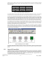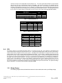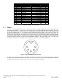
1
Xilinx® Virtex™-II Pro Development Kit User Guide Table of Contents 1.0 Introduction ............................................................................................................................................................................... 4 1.1 Description............................................................................................................................................................................ 4 1.2 Features: .............................................................................................................................................................................. 4 1.3 Demo Applications................................................................................................................................................................ 4 1.4 Ordering Information:............................................................................................................................................................ 5 2.0 User Information ....................................................................................................................................................................... 5 2.1 Power ................................................................................................................................................................................... 5 2.2 Configuration ........................................................................................................................................................................ 5 2.2.1 Boundary-scan............................................................................................................................................................. 5 2.2.2 System ACE CompactFlash ........................................................................................................................................ 6 2.2.3 PCI............................................................................................................................................................................... 7 2.3 Jumper Settings.................................................................................................................................................................... 8 3.0 Hardware .................................................................................................................................................................................. 9 3.1 Virtex-II Pro FPGA.............................................................................................................................................................. 10 3.2 High-speed Serial Communication ..................................................................................................................................... 10 3.2.1 HSSDC2 .................................................................................................................................................................... 10 3.2.2 SFP............................................................................................................................................................................ 10 3.2.3 XPAK ......................................................................................................................................................................... 11 3.3 Memory .............................................................................................................................................................................. 13 3.3.1 Mobile SDRAM .......................................................................................................................................................... 13 3.3.2 Asynchronous SRAM................................................................................................................................................. 14 3.3.3 Flash .......................................................................................................................................................................... 14 3.3.4 DDR SDRAM SODIMM ............................................................................................................................................. 14 3.3.5 System ACE CompactFlash ...................................................................................................................................... 15 3.4 Communication................................................................................................................................................................... 16 3.4.1 Ethernet PHY ............................................................................................................................................................. 16 3.4.2 RS232 Transceiver .................................................................................................................................................... 17 3.5 PCI ..................................................................................................................................................................................... 18 3.5.1 Bridge Design ............................................................................................................................................................ 18 3.5.2 PCI Utility ................................................................................................................................................................... 21 3.6 I/O Connectors ................................................................................................................................................................... 21 3.6.1 AvBus Connectors ..................................................................................................................................................... 22 3.6.2 PMC Connectors ....................................................................................................................................................... 22 3.6.3 Header “JP16” ........................................................................................................................................................... 22 3.7 Power ................................................................................................................................................................................. 28 3.8 Configuration ...................................................................................................................................................................... 29 4.0 Software/BSP.......................................................................................................................................................................... 29 4.1 What is included ................................................................................................................................................................. 30 4.2 PLB Memory Project........................................................................................................................................................... 30 4.3 OPB Memory Project .......................................................................................................................................................... 31 4.4 MGT Peripheral Project ...................................................................................................................................................... 31 4.5 Ethernet Peripheral Discussion .......................................................................................................................................... 31 4.6 Avmon Debug Monitor ........................................................................................................................................................ 33 4.7 Board Support Package for Linux....................................................................................................................................... 33 5.0 List of partners ........................................................................................................................................................................ 33 Copyright © 2003 Avnet, Inc. AVNET and the AV logo are registered trademarks of Avnet, Inc. All other trademarks are property of their respective owners. Avnet Electronics Marketing Released 2 of 33 Rev 1.0 04/18/2006 Literature # ADS-003704 Figures Figure 1 - Virtex-II Pro Development Board Picture ................................................................................................................................... 5 Figure 2 - Boundary-scan Chain in iMPACT............................................................................................................................................... 6 Figure 3 - Virtex-II Pro Development Board Block Diagram ....................................................................................................................... 9 Figure 4 – Jumper Pad Pin-out................................................................................................................................................................. 17 Figure 5 – Bridge Design Block Diagram.................................................................................................................................................. 19 Figure 6 - High-Current Power Connector "J19"....................................................................................................................................... 28 Figure 7 - Barrel Power Connector "J7".................................................................................................................................................... 29 Tables Table 1 - Ordering Information ................................................................................................................................................................... 5 Table 2 - JTAG Headers (JTAG3 & JTAG4) Pin-Out ................................................................................................................................. 6 Table 3 - Virtex-II Pro Attributes by Density/Speed Grade ....................................................................................................................... 10 Table 4 - HSSDC2 Connector Pin-outs (P2 & P3).................................................................................................................................... 10 Table 5 - SFP Connectors Pin-outs (P4 & P5) ......................................................................................................................................... 11 Table 6 - XPAK Host Connector Pin-out (P1)........................................................................................................................................... 12 Table 7 - Timing Parameters for SDRAM Peripheral................................................................................................................................ 14 Table 8 - Timing Parameters for Flash Peripheral.................................................................................................................................... 14 Table 9 - System ACE: MPU Interface Connections ................................................................................................................................ 16 Table 10 - Ethernet PHY Strapping Options............................................................................................................................................. 17 Table 11 - RS232 FPGA Pin-out .............................................................................................................................................................. 18 Table 12 - RS232 Connector Pin-out ....................................................................................................................................................... 18 Table 13 - Custom Serial Cable Pin-out ................................................................................................................................................... 18 Table 14 - PCI Memory Map .................................................................................................................................................................... 19 Table 15 - Control Register Bit Map ......................................................................................................................................................... 20 Table 16 - Status Register Bit Map........................................................................................................................................................... 21 Table 17 - AvBus Connectors Available by Virtex-II Pro Density.............................................................................................................. 22 Table 18 - AvBus Connector "P8" Pin-out ................................................................................................................................................ 23 Table 19 - AvBus Connector "P10" Pin-out .............................................................................................................................................. 24 Table 20 - AvBus Connector "P11" Pin-out .............................................................................................................................................. 25 Table 21 - AvBus Connector "P12" Pin-out .............................................................................................................................................. 26 Table 22 - PMC Connector "P6" Pin-out................................................................................................................................................... 27 Table 23 - PMC Connector "P7" Pin-out................................................................................................................................................... 27 Table 24 - Header "JP16" Pin-out ............................................................................................................................................................ 28 Table 25 - JTAG Chain Selection "JP15" ................................................................................................................................................. 29 Table 26 - PLB Memory Project - Memory Map ....................................................................................................................................... 30 Table 27 - OPB Memory Project - Memory Map....................................................................................................................................... 31 Copyright © 2003 Avnet, Inc. AVNET and the AV logo are registered trademarks of Avnet, Inc. All other trademarks are property of their respective owners. Avnet Electronics Marketing Released 3 of 33 Rev 1.0 04/18/2006 Literature # ADS-003704 1.0 Introduction The purpose of this manual is to describe the functionality and contents of the Virtex-II Pro Development Kit from Avnet Electronics Marketing. This document includes instructions for operating the board, descriptions of the hardware features and explanations of the example projects. 1.1 Description The Virtex-II Pro Development Kit provides a development platform for engineers designing with the Xilinx Virtex-II Pro FPGA. The board provides the necessary hardware to not only evaluate the advanced features of the Virtex-II Pro but also to implement complete user applications. Example projects are provided to help the user understand the design tool flow of the Xilinx Embedded Development Kit (EDK) software environment. 1.2 Features: FPGA Xilinx Virtex-II Pro XC2VP7/20/30-FF896 High-speed Serial Communication Two HSSDC2 connectors (InfiniBand, user may replace with Fibre Channel) Pads for a XPAK module (10Gb Ethernet, OC-192) Receptacles for two SFP modules (Gigabit Ethernet, Fibre Channel, InfiniBand) Memory Micron DDR SDRAM SODIMM (128MB expandable to 1GB) Micron Mobile SDRAM (two 8Mbit x 16 devices, 32MB total) Cypress Asynchronous SRAM (512Kbit x 32, 2MB total) Intel StrataFlash (16MB total) CompactFlash Card Communication National 10/100/1000 Mbit/s Ethernet PHY RS-232 serial ports PCI PCI Bridge - Xilinx Spartan-IIE XC2S300E-FG456 FPGA Windows based GUI interface Configuration or File Transfer & System Control Universal PCI Connector (32-bit or 64-bit slot compatible) Support for both 3.3V and 5.0V PCI signaling Board I/O Connectors 32bit PCI Mezzanine Card (PMC) Connectors Four 140-pin general purpose I/O expansion connectors (AvBus) Power Power Supply Daughter card (+3.3V and +2.5V rails @ 14A total) 50 Watt AC/DC +5.0V power supply National Linear regulators Configuration Bridge (Spartan-IIE) o Xilinx PROM XC18V02-VQ44 Target (Virtex-II Pro) o Xilinx System ACE CF o FLASH or SRAM via PCI and Windows Application 1.3 Demo Applications The Virtex-II Pro Development Kit from Avnet Electronics Marketing comes with example projects designed in Xilinx Platform Studio (XPS). XPS is a software tool in the Xilinx Embedded Development Kit that provides the user with a single tool flow for creating both hardware and software systems. The example projects help the user to more quickly learn the XPS tool and develop user-specific applications by leveraging already tested and functional designs. The example projects that will be discussed in detail later in this document are listed below. Memory Projects o Two memory projects: OPB memory project and PLB memory project o OPB memory project is a hardware system for PowerPC access to SRAM, Flash and SDRAM o PLB memory project is a hardware system for PowerPC access to SDRAM via the PLB Rocket I/O (MGT) Peripheral Project o Custom peripheral that enables PowerPC access to a Multi-Gigabit Transceiver o Uses generic protocol to send/receive data at up to 3.125 Gbps o Includes control interface for SFP modules Copyright © 2003 Avnet, Inc. AVNET and the AV logo are registered trademarks of Avnet, Inc. All other trademarks are property of their respective owners. Avnet Electronics Marketing Released 4 of 33 Rev 1.0 04/18/2006 Literature # ADS-003704 Figure 1 - Virtex-II Pro Development Board Picture 1.4 Ordering Information: The following table lists the development system part numbers and available software options. Internet link at http://www.em.avnet.com/ads Part Number ADS-XLX-V2PRO-DEVP7-6 ADS-XLX-V2PRO-DEVP20-6 ADS-XLX-V2PRO-DEVP30-6 Hardware Virtex-II Pro Development Kit with a XC2VP7, -6 Speed Grade Virtex-II Pro Development Kit with a XC2VP20, -6 Speed Grade Virtex-II Pro Development Kit with a XC2VP30, -6 Speed Grade Table 1 - Ordering Information 2.0 User Information This section provides the user with information on how to get started using the Virtex-II Pro Development board. It discusses how to power the board, configure the FPGA devices and set-up the jumpers. 2.1 Power The Virtex-II Pro Development Kit includes a 50-Watt AC/DC Converter that plugs into the power supply daughter-board on the backside of the Virtex-II Pro Development board. The daughter-board is labeled “14A Programmable Power Supply” and the AC/DC Converter plugs into the high-current connector labeled “J9”. The high-current connector is keyed to protect the board therefore it is only possible to insert the power connector the correct way. When the plug is inserted into the daughter-board and the AC power cord is plugged in to an outlet, power is applied to the board. It is recommended to plug the AC power cord of the Converter into a power strip with an On/Off switch to more easily cycle power to the board. 2.2 Configuration The Virtex-II Pro Development board supports three different methods for configuring (programming) the Virtex-II Pro FPGA. These methods include Boundary-scan, System ACE CompactFlash and PCI. 2.2.1 Boundary-scan Programming the Virtex-II Pro FPGA via Boundary-scan requires a JTAG download cable (not included in the kit). The Virtex-II Pro Development board has connectors to support both the flying leads connection of the Parallel Cable III and MultiLINX cables, and the ribbon cable connection of the Parallel Cable IV. These connectors are labeled JTAG3 (JP14) and JTAG4 (JP12) respectively. For more information about JTAG download cables see the Xilinx web page http://www.xilinx.com. Click on the “Products” tab and then click on the “Configuration” link. Scroll down to “Desktop Programmers and Download Cables” and select the download cable of interest. When using the flying leads connection of the Parallel Cable III or MultiLINX, connect the leads according to the silkscreen labels on JTAG3 (JP14). These connections are shown in Table 2 below. Pin 1 of JTAG3 is a dualCopyright © 2003 Avnet, Inc. AVNET and the AV logo are registered trademarks of Avnet, Inc. All other trademarks are property of their respective owners. Avnet Electronics Marketing Released 5 of 33 Rev 1.0 04/18/2006 Literature # ADS-003704 purpose pin that can either be used as VCC when using a cable that requires a VCC input or as TRST, the TAP reset line, for cables requiring access to TRST. Place a jumper (shunt) on JP17 across pins 1-2 to connect the dualpurpose pin to VCC. Signal Name VCC TDI TDO TMS TCK GND JTAG3 (JP14) pin 1 3 5 7 9 2,4,6,8 or 10 JTAG4 (JP12) pin 2 10 8 4 6 1,3,5,7,9,11 or 13 Table 2 - JTAG Headers (JTAG3 & JTAG4) Pin-Out If the Parallel Cable IV is used, the ribbon cable connector mates with the JTAG4 (JP12) connector. The connectors are keyed to ensure the connections are made correctly. Table 2 also shows the pin-out of the JTAG4 connector. The Virtex-II Pro Development board provides the user with the ability to add/remove devices from the JTAG chain. By the default settings, the chain includes the System ACE controller, the Virtex-II Pro FPGA, the XC18V02 PROM and the Spartan-IIE FPGA. The header labeled “JP15” allows the user to select what devices are in the chain. This will be discussed in greater detail in the hardware section of this manual. Most users will only use the JTAG chain in standalone mode with a jumper installed across pins 2-3 on JP15. It is recommended to start with standalone mode. The configuration modes of the FPGAs must be selected before applying power to the board. The Virtex-II Pro FPGA is set to boundary-scan mode by default (no jumper installed on JP8). To program the Spartan-IIE FPGA directly via boundary-scan, place a jumper on JP9 to set for boundary-scan mode. Remove the jumper on JP9 to set for masterserial mode to load the Spartan-IIE from the PROM on power-up. After the download cable, chain and modes have been set; apply power to the board and open/run the iMPACT software to configure the boundary-scan devices. It is recommended to use the version of iMPACT in the Xilinx ISE 5.1i or later tools. Earlier versions of the tools may work but the user will have to add the chain manually instead of using the automatic chain initialization. Figure 2 - Boundary-scan Chain in iMPACT The iMPACT software will auto-detect the Spartan-IIE FPGA as a Virtex-E device. When the user assigns a bit file targeting the Spartan-IIE device, iMPACT will bring up a warning about the part assignment change that can safely be ignored. 2.2.2 System ACE CompactFlash Configuring the Virtex-II Pro FPGA with the System ACE CompactFlash is an easy and convenient way of transferring bit files from the design environment to the development board. The user will need a CompactFlash card reader or PCMCIA-to-CompactFlash card adapter to be able to copy files from a PC/laptop computer to the CompactFlash card. The configuration process involves three steps: preparing the System ACE files, copying the files to the CompactFlash card and running the System ACE controller. Copyright © 2003 Avnet, Inc. AVNET and the AV logo are registered trademarks of Avnet, Inc. All other trademarks are property of their respective owners. Avnet Electronics Marketing Released 6 of 33 Rev 1.0 04/18/2006 Literature # ADS-003704 If the user wants to skip the process of preparing their own card, the CompactFlash card is initially programmed with demo/test files. Set the CFG MODE switch on the dipswitch labeled “S1” to the OFF position, set the CFG ADDR with the three switches (switch 1 is the LSB), and set switch 1 on the dipswitch labeled “S2” to the ON position and then apply power to the board. The DONE LED labeled “D22” will light to indicate a successful configuration of the Virtex-II Pro FPGA. The iMPACT software in the Xilinx ISE 5.1i or later tool set is used to prepare the System ACE files. After opening the iMPACT program, select the option for “Prepare Configuration Files”. Next select “System ACE File” and then choose the target device on the next window to be “System ACE CF”. Start with the “Novice” user mode and try the expert mode after becoming familiar with the process. Set the card size to “Generic” since the CompactFlash card is a non-Xilinx card and larger than the density options. Set the “Reserve Space” to 0 initially. The reserve space is the space leftover on the CompactFlash card after storing the bit files, which can be used by the Virtex-II Pro FPGA as non-volatile memory. Next give the Flash card build a name and specify a location for the generated files (this can be the CompactFlash card itself or a directory to save the files before copying to the card). Next select the address locations to be used based on the number of bit files being used. Give each address location a name corresponding to the bit file for that location (limit 8 characters on names). Click next to start adding bit files. Click on “Add File” and browse to the location of your first bit file (address 0). Click on “No” when prompted to add another design file to the address (only use one bit file per address). Repeat the process to add the rest of the bit files and then click “Finish” to start generating the System ACE files. After generating the files, the user needs to set up their CompactFlash card reader or PCMCIA adapter to connect the CompactFlash card to a PC or laptop. Remove the CompactFlash card from the development board by pulling it out by the top edge. There is no release mechanism. Follow the instructions that came with the card reader or adapter for set-up. Once the CompactFlash card is detected (should show up as another drive), become familiar with the System ACE file structure by looking at the demo files already on the CompactFlash card. After looking at the files, delete them so they do not conflict with the files about to be added to the card. Do not worry about losing the System ACE demo files, they are on the CD that came with the kit. Finally, copy the files generated by iMPACT, from the location specified during file preparation, and paste them in the CompactFlash directory. The CompactFlash card is now ready to be inserted in the Virtex-II Pro Development board. Plug the CompactFlash card into the socket labeled “P9”. The socket is located on the backside of the Virtex-II Pro Development board underneath the power supply daughter board. Do not force the card in the socket. If having trouble with insertion just turn the card over and try it. The card is keyed and will only fit one way. Before applying power to the board, set the following switches. Set the CFG MODE switch on the dipswitch labeled “S1” to the default position (OFF). This will set the System ACE controller to load the Virtex-II Pro on power-up (when released out of reset). Next set the CFG ADDR switches to the address of the bit file to be loaded. Switch 3 is the MSB and switch 1 is the LSB. A switch in the OFF position is a low or binary ‘0’ (all CFG ADDR switches off is address 0x0). Finally set switch 1 on the dipswitch labeled “S2” to the ON position to release the System ACE from reset and apply power to the board. The DONE LED for the Virtex-II Pro FPGA, “D22”, should be illuminated to indicate a successful configuration. Also, the System ACE Status LED labeled “D8” will illuminate upon a successful System ACE configuration of the Virtex-II Pro. The System ACE Error LED labeled “D9” will illuminate if an error occurs. The Error LED will also blink if the CompactFlash card is not plugged in. To re-load the FPGA with a bit file at a different address, change the CFG ADDR switches to the desired address and then toggle switch 1 on dipswitch “S2” OFF then ON to reset the System ACE controller. 2.2.3 PCI The Virtex-II Pro FPGA can be configured over PCI by running the Avnet Electronics Marketing PCI Utility, a graphical user interface that allows the user to read/write and download files to the PCI memory space in addition to configuring the Virtex-II Pro FPGA. The purpose of the configuration over PCI is to allow the user to put the board into the PCI slot of their development PC, close the lid to the PC chassis and be able to work with the board without it taking up counter space. It is also a very fast way of reconfiguring the Virtex-II Pro device. Place a jumper (shunt) on “JP8” to put the Virtex-II Pro FPGA in SelectMAP mode. This is required for configuration over PCI. Also, make sure the System ACE controller is in reset by putting switch 1 of the dipswitch labeled “S2” in the OFF position. The PROM file for the PCI bridge design must be programmed into the XC18V02 PROM (the board comes with the PROM already programmed with the bridge design). Finally, make sure the Spartan-IIE is set for master-serial mode to load from the PROM on power-up (remove jumper on JP9). The Virtex-II Pro Development board was designed to fit into the majority of computer cases with PCI support. The board is 600 mils (0.6 inches) taller than the PCI specification requirement and may not fit in all cases. To install the development board into a computer case, turn the power off to the computer and remove the cover on the case. Leave the power cord connected to the outlet. Next using a static strap or touching the bare metal of the computer chassis to discharge static build-up, insert the development board into an open PCI slot. The Virtex-II Pro Development board requires two PCI slots since the daughter-board protrudes over the adjacent slot. The power supply daughter-board must be connected to the development board since it supplies the 2.5VDC rail. Do not plug the AC/DC converter into the daughter-board. Power is derived from the PCI slot when plugged in. Make sure the Copyright © 2003 Avnet, Inc. AVNET and the AV logo are registered trademarks of Avnet, Inc. All other trademarks are property of their respective owners. Avnet Electronics Marketing Released 7 of 33 Rev 1.0 04/18/2006 Literature # ADS-003704 development board is firmly seated in the PCI slot and that it is not touching any bare metal components in the computer case. Replace the cover and turn on the computer. Copy the PCI Utility folder from the CD that comes with the kit to the local drive of the computer containing the VirtexII Pro Development board. The ADS PCI Utility User Manual inside the folder contains the installation instructions. After installation is complete, run the PCI Utility program. In the PCI Utility window, the “Open Board” field should indicate the Virtex-II Pro Development board has been detected. To configure the Virtex-II Pro FPGA, click the downward arrow to expand the “Mode” menu and select “Configure” from the list. A browse window will open to prompt the user to browse to the location of the bit file to be programmed into the Virtex-II Pro. Select a bit file and then click on “Execute” to start the programming operation. A window will pop-up in a moment indicating the result of the configuration. There is no need to look at the DONE LED since the Utility reads the level of the DONE pin to determine if the configuration was successful. When generating a bit file to be used with the PCI Utility, use CCLK as the startup clock. Configuration will fail to complete if a bit file was used with the startup clock set to JTAG clock (CCLK is the default setting in the Xilinx ISE tools). To set the startup clock in Project Navigator, right-click on “Generate Programming File” in the “Processes for Current Source:” window and select “Properties”. Next click on the “Startup options” tab and select CCLK under the “FPGA Start-Up Clock” field. Then run the programming file generation step. 2.3 Jumper Settings This section provides a description of the jumper settings for the development board. The jumpers are listed by the silkscreen labels on the board. The board is ready to use out of the box with the default jumper settings. SFP0 TX EN – JP3 Install a jumper on “JP3” to enable transmission of SFP module #0 in the EMI cage labeled “P4”. Remove the jumper to disable transmit. Default: Open; TX disabled. SFP1 TX EN – JP2 Install a jumper on “JP2” to enable transmission of SFP module #1 in the EMI cage labeled “P5”. Remove the jumper to disable transmit. Default: Open; TX disabled. TRGT CFG MODE – JP8 Sets the configuration mode of the Virtex-II Pro FPGA. Remove the jumper for boundary-scan mode. Install a jumper for SelectMAP mode, which is used by the PCI Utility during configuration. Default: Open; boundary-scan mode. BRIDGE CFG MODE – JP9 Sets the configuration mode of the Spartan-IIE FPGA. Remove the jumper for master-serial mode and the PROM will load the Spartan-IIE on power-up. Install a jumper for boundary-scan mode to program the Spartan-IIE directly via boundary-scan. Default: Open; master-serial mode. HSWAP EN – JP11 Enables pull-ups on the Virtex-II Pro I/O pins during configuration. Install a 0 ohm, 0603 resistor to disable the configuration pull-ups (I/Os will be floating). Do not install a resistor to enable the configuration pull-ups. Default: Open; pull-ups enabled. APS VOLTAGE – JP5 Allows the user to select the voltage level for the APS supply to the XPAK module. The Virtex-II Pro Development board does not implement a fully adjustable power supply for the XPAK module. Instead the board supplies two of the common voltages used by XPAK modules. Install a jumper across pins 1-2 to set the APS voltage to 1.2VDC. Install a jumper across pins 2-3 to set the APS voltage to 1.8VDC. The APS regulator is in shutdown mode until an XPAK mode is present. Default: Open when XPAK module not installed; 0VDC output. TRST/VCC – JP17 Sets the mode of the dual-purpose pin on the JTAG3 header. The center pin is the TRST signal that is connected to the TRST pin of the Ethernet PHY and also pin 1 of the JTAG3 header. Install a jumper across pins 1-2 to set pin 1 of JTAG3 to VCC (3.3VDC) and tie the TRST signal high (used during boundary-scan programming with JTAG3 header). Do not install a jumper to float the TRST signal for external control (used with boundary-scan tools that require control of TRST). Install a jumper across pins 2-3 to pull the TRST signal low (used to put the Ethernet PHY in normal operation). Default: Installed across pins 2-3; normal operation of Ethernet PHY. JTAG CHAIN – JP15 Copyright © 2003 Avnet, Inc. AVNET and the AV logo are registered trademarks of Avnet, Inc. All other trademarks are property of their respective owners. Avnet Electronics Marketing Released 8 of 33 Rev 1.0 04/18/2006 Literature # ADS-003704 Selects the JTAG chain configuration. Install a jumper across pins 2-3 for standalone mode (4 devices in chain: System ACE, Virtex-II Pro, XC18V02 PROM and Spartan-IIE FPGA). Install jumpers across pins 1-2 and pins 4-5 to add the PMC connectors on to the standalone chain. Install jumpers across pins 1-2, pins 3-4 and pins 5-6 to add the AvBus connector labeled “P10” on to the standalone chain. These settings are described in detail in the Hardware section of this manual. Default: Installed across pins 2-3; standalone chain mode. 3.0 Hardware This section of the manual describes the hardware of the Virtex-II Pro Development board. The hardware was designed with the VirtexII Pro FPGA as the focal point. The block diagram is shown in Figure 3. Figure 3 - Virtex-II Pro Development Board Block Diagram Copyright © 2003 Avnet, Inc. AVNET and the AV logo are registered trademarks of Avnet, Inc. All other trademarks are property of their respective owners. Avnet Electronics Marketing Released 9 of 33 Rev 1.0 04/18/2006 Literature # ADS-003704 3.1 Virtex-II Pro FPGA The Virtex-II Pro Development board was designed to support the Virtex-II Pro FPGA in the 896-pin, flip-chip BGA package (FF896). The flip-chip package provides superior multi-gigabit transceiver (MGT) performance over the wire bond package, providing data rates up to 3.125 Gbps in the –6 and –7 speed grades. The FF896 package is a versatile package with three mid-range densities providing eight MGTs and up to 556 I/Os and two embedded PowerPC processors. The board was designed to support all three densities: the 2VP7, 2VP20 and 2VP30. The schematic symbol used for the Virtex-II Pro device indicates the specific I/O pins available in each density (396 I/Os with 2VP7 and 556 I/Os with the 2VP20/30). The Virtex-II Pro Development board is available with different device options. Table 3 describes the attributes of the Virtex-II Pro device based on density and speed grade. Virtex-II Pro Part (FF896 pkg.) XC2VP7 XC2VP20 XC2VP30 I/O MGT 396 556 556 8 8 8 PowerPC Cores 1 2 2 MGT/PowerPC Performance by Speed Grade -7 -6 -5 3.125 Gbps/400MHz 3.125 Gbps/350MHz 2.0 Gbps/300MHz 3.125 Gbps/400MHz 3.125 Gbps/350MHz 2.0 Gbps/300MHz 3.125 Gbps/400MHz 3.125 Gbps/350MHz 2.0 Gbps/300MHz Table 3 - Virtex-II Pro Attributes by Density/Speed Grade 3.2 High-speed Serial Communication The MGTs of the Virtex-II Pro FPGA are connected to two HSSDC2 connectors, two Small Form Pluggable (SFP) connectors with EMI cages, and pads for a XPAK host connector with mounting holes for the mid-board module holder. In the case of the two HSSDC2 and two SFP connections, the MGTs were treated individually. This means the lengths of the transmit and receive signals were matched per MGT but not matched to any other MGT. However, in the case of the XPAK interface, four MGT channels were bonded together to create the 10-Gigabit Attachment Unit Interface (XAUI). The four transmit pairs have matched lengths and the four receive pairs have matched lengths. Each high-speed connector is described in greater detail in the following sub-sections. 3.2.1 HSSDC2 The HSSDC2 connectors are used to implement high-speed serial communication over copper. These connectors support data rates up to 2.5 Gbps and are typically used for the Infiniband or Fibre Channel communication standards. The connectors are labeled “P2” and “P3” on the board. The pin-outs are shown below. The connectors installed on the board are keyed for Infiniband cables. The user may replace them with connectors keyed for Fibre Channel cables if desired since they have the same footprint. Pin # 1 2 3 4 5 6 7 P2 Signal (V2Pro pin) AGND RX_P (A25) RX_N (A24) AGND TX_N (A27) TX_P (A26) AGND Pin # 1 2 3 4 5 6 7 P3 Signal (V2Pro pin) AGND RX_P (A18) RX_N (A17) AGND TX_N (A20) TX_P (A19) AGND Table 4 - HSSDC2 Connector Pin-outs (P2 & P3) Table 4 gives the actual pin numbers in parenthesis of the MGT pins on the Virtex-II Pro FPGA. To implement a highspeed serial protocol at 2.5 Gbps, use the 125MHz differential clock input for the reference clock to the MGT macro. This clock is brought in on a BREF clock site, which has optimized routing to the MGT clock PLL. The clock net names are GIGE_CLK_P and GIGE_CLK_N with FPGA pin numbers of “F16” and “G16” respectively. The transmit pairs on both connectors are DC coupled but have 0 ohm, 0603 resistors that could be replaced with capacitors to AC couple the lines. The receive pairs are AC coupled by default. 3.2.2 SFP The SFP host connector and EMI cages can be used to implement a high-speed serial protocol over optical fiber or copper depending on the module used. These connectors support data rates up to 2.5 Gbps and can be used for Gigabit Ethernet, Infiniband or Fibre Channel. The connectors are labeled “P4” and “P5” on the board. The pin-outs are shown below. Copyright © 2003 Avnet, Inc. AVNET and the AV logo are registered trademarks of Avnet, Inc. All other trademarks are property of their respective owners. Avnet Electronics Marketing Released 10 of 33 Rev 1.0 04/18/2006 Literature # ADS-003704 Pin # 1 2 3 4 5 6 7 8 9 10 P4 (SFP#1) Signal (V2Pro Pin) Pin # AGND 11 TX_FAULT (F8) 12 TX_DISABLE 13 MOD_DEF2 14 MOD_DEF1 15 MOD_DEF0 16 RATE_SEL 17 LOS (F7) 18 AGND 19 AGND 20 Signal (V2Pro Pin) AGND RX_N (A4) RX_P (A5) AGND VCCR VCCT AGND TX_P (A6) TX_N (A7) AGND Pin # 1 2 3 4 5 6 7 8 9 10 P5 (SFP#0) Signal (V2Pro Pin) Pin # AGND 11 TX_FAULT (E9) 12 TX_DISABLE 13 MOD_DEF2 14 MOD_DEF1 15 MOD_DEF0 16 RATE_SEL 17 LOS (E8) 18 AGND 19 AGND 20 Signal (V2Pro Pin) AGND RX_N (A11) RX_P (A12) AGND VCCR VCCT AGND TX_P (A13) TX_N (A14) AGND Table 5 - SFP Connectors Pin-outs (P4 & P5) Table 5 shows the actual pin numbers in parenthesis of the MGT pins on the Virtex-II Pro FPGA. Two of the control signals, Transmit Fault and Loss Of Signal, are connected directly to the FPGA. The FPGA pin numbers for these signals are shown in Table 5. The Transmit Disable pins are connected to two-pin headers for jumper selection. These pins are pulled high to disable transmission as the default. Install jumpers on “JP2” and/or “JP3” to enable transmission of the SFP module(s). The remaining control signals were not connected to the FPGA due to pin limitations. These signals are brought out to test pads for the user to probe or solder test wires To implement a high-speed serial protocol at 2.5 Gbps, use the 125 MHz differential clock input for the reference clock to the MGT macro. This clock is brought in on a BREF clock site, which has optimized routing to the MGT clock PLL. The clock net names are GIGE_CLK_P and GIGE_CLK_N with FPGA pin numbers of “F16” and “G16” respectively. Since the PLL of the MGT always multiplies by a factor of 20, using the 125 MHz clock results in a transmission rate of 2.5 Gbps. To run at a slower rate, the user may divide the clock using a Digital Clock Manager (DCM) and run the input into the reference clock on the MGT macro. This will introduce jitter, however, and is not recommended for data rates above 1.25 Gbps. A better approach would be to find an alternate oscillator with a lower frequency to replace the 125 MHz oscillator on the board. Care must be taken in device selection for output voltage (2.5VDC) and pin-out compatibility (LVPECL/LVDS differential output). Both the transmit and receive pairs are directly connected or DC coupled to the SFP host connectors. Typically both the transmit and receive pairs are AC coupled inside the SFP module. The SFP module is powered by the 3.3VDC supply with separate filtering networks for the transmit and receive supplies (VccT and VccR). The transmit and receive ground terminals (VeeT and VeeR) are both connected to the same AGND reference. 3.2.3 XPAK The XPAK is a small form factor pluggable transceiver module for 10 Gbps serial data transmission. The XPAK interface on the Virtex-II Pro Development board was designed to run at the IEEE 10GBASE-R optical rate of 10.3125 Gbps with a four lane electrical interface at 3.125 Gbps (XAUI interface). This interface requires a –6 or –7 speed grade Virtex-II Pro device and has not been fully tested. Furthermore, the 10 Gigabit Ethernet MAC core from Xilinx takes up considerable resources and may not fit in the 2VP7 density. The –5 speed grade part cannot be expected to run at 10.3125 Gbps since the MGTs are only rated at 2.0 Gbps. The XPAK interface on the Virtex-II Pro Development board was designed to comply with the XPAK MSA Revision 2.1, with some exceptions to be discussed later. The XPAK MSA closely resembles the XENPAK MSA and makes frequent references to it. The XPAK form factor was used because its half the size of a XENPAK, it does not require a large cut-out in the PCB and it has a midboard mounting option allowing the module to be placed anywhere on the board instead of on the faceplate. The XPAK connector is labeled “P1” and is located on the backside (solder-side) of the board. The pin-out of the host connector is shown below. Copyright © 2003 Avnet, Inc. AVNET and the AV logo are registered trademarks of Avnet, Inc. All other trademarks are property of their respective owners. Avnet Electronics Marketing Released 11 of 33 Rev 1.0 04/18/2006 Literature # ADS-003704 Pin # 1 2 3 4 5 6 7 8 9 10 11 12 13 14 15 16 17 18 19 20 21 22 23 24 25 26 27 28 29 30 31 32 33 34 35 P1 (XPAK host connector) Signal (FPGA pin) Pin # Signal (FPGA pin) AGND 36 AGND AGND 37 AGND AGND 38 N/C 5VDC 39 N/C 3.3VDC 40 AGND 3.3VDC 41 RX0_P (AK5) APS 42 RX0_N (AK4) APS 43 AGND XAUI_LASI (AH5) 44 RX1_P (AK12) XAUI_RESET 45 RX1_N (AK11) N/C 46 AGND TX ON/OFF 47 RX2_P (AK18) N/C 48 RX2_N (AK17) MOD_DET 49 AGND N/C 50 RX3_P (AK25) N/C 51 RX3_N (AK24) XAUI_MDIO (F21) 52 AGND XAUI_MDC (H21) 53 AGND PRTAD4 54 AGND PRTAD3 55 TX0_P (AK6) PRTAD2 56 TX0_N (AK7) PRTAD1 57 AGND PRTAD0 58 TX1_P (AK13) N/C 59 TX1_N (AK14) APS_SET 60 AGND N/C 61 TX2_P (AK19) APS_SENSE 62 TX2_N (AK20) APS 63 AGND APS 64 TX3_P (AK26) 3.3VDC 65 TX3_N (AK27) 3.3VDC 66 AGND 5VDC 67 N/C AGND 68 N/C AGND 69 AGND AGND 70 AGND Table 6 - XPAK Host Connector Pin-out (P1) Table 6 gives the actual pin numbers in parenthesis of the MGT pins on the Virtex-II Pro FPGA. The management interface signals (MDIO and MDC) are connected to the Virtex-II Pro FPGA through level shifting logic. It is necessary to shift the voltage level of the XPAK outputs from the APS voltage level (1.2V or 1.8V) to 2.5VDC to meet the minimum input level of the FPGA. Likewise the outputs of the FPGA are shifted down to the APS supply voltage. Since the MDIO signal is a bi-directional data line, it was necessary to add a direction control signal. This signal is called XAUI_MDIO_DIR and is connected to pin “D15” of the Virtex-II Pro FPGA. Setting the direction pin low (logic ‘0’) enables the FPGA output buffer and disables the XPAK output buffer allowing the FPGA to drive the MDIO line. The opposite is true when setting the direction pin high (logic ‘1’), the XPAK is able to drive the MDIO line. The user should set the direction pin low to write to the MDIO line and high to read from the MDIO line. The Link Alarm Status Interrupt (LASI) pin is connected to the FPGA to allow detection of whether a module is installed. The Transmit On/Off pin is connected to a two-pin header for jumper selection. This pin is pulled down by default to disable transmission. Install a jumper on “JP1” to enable transmission. The Reset pin on the XPAK module is connected to the Spartan-IIE FPGA due to pin limitations on the Virtex-II Pro. The Bridge design in the Spartan-IIE FPGA sets the XPAK reset pin based on the setting of switch 2 on the dipswitch labeled “S2”. Turn switch 2 to the ON position to bring the XPAK module out of the reset state. The Virtex-II Pro Development board was designed to comply with the XPAK MSA Revision 2.1 with the major exception being the design of the Adjustable Power Supply (APS). The fully adjustable supply detailed in the XPAK MSA was not implemented. Instead an adjustable voltage regulator is used to supply two of the most common APS voltages based on a jumper setting. Place a jumper on “JP5” across pins 1-2 to generate an APS voltage of 1.2VDC, Copyright © 2003 Avnet, Inc. AVNET and the AV logo are registered trademarks of Avnet, Inc. All other trademarks are property of their respective owners. Avnet Electronics Marketing Released 12 of 33 Rev 1.0 04/18/2006 Literature # ADS-003704 or place the jumper across pins 2-3 for 1.8VDC. The user must select the APS voltage level based on the voltage requirements of the module being used. It is possible to generate an APS voltage other than the default levels of 1.2VDC and 1.8VDC by replacing either R112 or R113 with a different resistance value. See the datasheet for National’s LP3966ES-ADJ Linear Regulator for the equation to calculate acceptable resistor values. The minimum output voltage of the regulator is 1.2VDC. The shutdown pin of the APS regulator (U12) is driven by the XPAK module detect signal. This keeps the regulator in shutdown mode to save power when a module is not installed. The APS Sense and APS Set signals on the XPAK module are not used and brought out to test pads for user access. The Port Address signals (PRTAD[0:4]) are not used since the board only supports one module. The 156.25 MHz differential clock input is used for the reference clock to the MGT macro. This clock is brought in on a BREF clock site, which has optimized routing to the MGT clock PLL. The clock net names are XAUI_CLK_P and XAUI_CLK_N with FPGA pin numbers of “AH16” and “AJ16” respectively. Since the PLL of the MGT always multiplies by a factor of 20, using the 156.25 MHz clock results in a transmission rate of 3.125 Gbps. The transmit and receive signals are directly connected to the XPAK host connector or DC coupled. However, all XPAK compliant modules have AC coupling on both the transmit and receive signals inside the module itself. The transmit differential pairs are routed on the solder-side of the board while the receive pairs are routed on the component-side. This keeps the signals from crossing on the way to the XPAK connector. Return paths are provided by the analog ground planes in the layers directly adjacent to the outer layers. The analog ground planes are separate from the digital ground used for the rest of the components on the board, but are referenced to digital ground in several locations through ferrite beads. 3.3 Memory The Virtex-II Pro Development board has several types of volatile and non-volatile memory. The Virtex-II Pro FPGA has access to the following memory devices either directly or indirectly through the Spartan-IIE FPGA: Mobile SDRAM, Asynchronous SRAM, DDR SDRAM SODIMM, Flash and System ACE CompactFlash. To maximize the number of Virtex-II Pro I/O pins available for user applications, a single memory bus was used to access the SDRAM, SRAM, Flash and System ACE CompactFlash. This shared bus provides an individual chip select to each memory device but shares the data and address busses. The shared bus has three elements that contribute to the loading (i.e. the direct connections to the Virtex-II Pro), the Mobile SDRAM, the Spartan-IIE FPGA and the 32-bit buffer/transceiver. The Spartan-IIE design provides an almost transparent connection from the shared bus to the SRAM and Flash. The System ACE CompactFlash resides on the other side of the address/control buffer and data bus transceiver. The DDR SODIMM bus is separate from the shared bus and dedicated to the SODIMM. 3.3.1 Mobile SDRAM Two Micron Mobile SDRAM devices, part number: MT8V8M16LFFF-8, make up the 32-bit data bus. Mobile SDRAM devices were used to accommodate the low voltage requirement of the shared memory bus (2.5V). These devices support 2.5V core and I/O supplies (VDD and VDDQ). Attributes of the Mobile SDRAM interface are listed below. 32MB total (two 8 Meg x 16 devices), board supports addressing for up to 64MB 54-ball FBGA (8mm x 9mm) Board supplies 2.5V to VDD and VDDQ 8ns access time (CL = 3 @ 125 MHz, CL = 2 @ 100 MHz) The following table lists the timing parameters required to set up the SDRAM peripheral in EDK for 100 MHz operation (parameters are entered in the MHS file). If a timing parameter is left out of the peripheral instantiation, a default value is automatically used. The Software/BSP section of this manual has more information about setting up peripherals in EDK. Copyright © 2003 Avnet, Inc. AVNET and the AV logo are registered trademarks of Avnet, Inc. All other trademarks are property of their respective owners. Avnet Electronics Marketing Released 13 of 33 Rev 1.0 04/18/2006 Literature # ADS-003704 SDRAM peripheral – Timing Parameter C_SDRAM_TMRD C_SDRAM_TWR C_SDRAM_TCCD C_SDRAM_TRAS C_SDRAM_TRC C_SDRAM_TRFC C_SDRAM_TRCD C_SDRAM_TRRD C_SDRAM_TRP C_SDRAM_TREF C_SDRAM_REFRESH_NUMROWS C_SDRAM_CAS_LAT C_SDRAM_DWIDTH C_SDRAM_AWIDTH C_SDRAM_COL_AWIDTH C_SDRAM_BANK_AWIDTH C_xxx_CLK_PERIOD_PS Time (ps) or Number 2 15000 1 50000 100000 100000 20000 20000 20000 64 4096 2 32 12 9 2 10000 Table 7 - Timing Parameters for SDRAM Peripheral 3.3.2 Asynchronous SRAM A single Cypress Asynchronous SRAM device, part number: CY7C1062AV33-12BGC, makes up the 32-bit data bus. The Cypress device provides 2 MB of SRAM memory on a single IC and is organized as 512K x 32. The device has an operating voltage of 3.3V and a –12 speed grade for 80 MHz operation. The SRAM is connected to the SpartanIIE FPGA via a dedicated bus. The Bridge design in the Spartan-IIE FPGA essentially connects the shared bus to the SRAM bus during Virtex-II Pro transactions to SRAM. The Bridge design also maps the SRAM into the BAR0 memory space and arbitrates transactions by the Virtex-II Pro and the PCI. The default timing parameters can be used to set up the external memory controller peripheral for the SRAM device. It is only necessary to specify the address location, OPB clock frequency and the port mappings. See the Software/BSP section of this manual for more information. 3.3.3 Flash The board has a dual footprint allowing either Intel StrataFlash or AMD Uniform Sector Flash to be used based on availability. Two 64 Mbit devices, 4M x 16, make up the 32-bit Flash data bus. The part number for the Intel StrataFlash device is E28F640J3A-120. The part number for the AMD Uniform Sector Flash device is AM29LV641DL90REI. Both devices have an operating voltage of 3.3V and provide 16 MB total of Flash memory. The Flash is connected to the Spartan-IIE FPGA via a dedicated bus. The Bridge design in the Spartan-IIE FPGA essentially connects the shared bus to the Flash during Virtex-II Pro transactions to Flash. The Bridge design also maps the Flash into the BAR1 memory space and arbitrates transactions by the Virtex-II Pro and the PCI. The timing parameters to set up the external memory controller (EMC) peripheral for the Flash devices are shown below. If a timing parameter is left out of the peripheral instantiation, a default value is automatically used. The Software/BSP section of this manual has more information about setting up peripherals in EDK. EMC peripheral – Timing Parameter C_READ_ADDR_TO_OUT_SLOW_PS_0 C_WRITE_ADDR_TO_OUT_SLOW_PS_0 C_WRITE_MIN_PULSE_WIDTH_PS_0 C_READ_ADDR_TO_OUT_FAST_PS_0 C_WRITE_ADDR_TO_OUT_FAST_PS_0 C_READ_RECOVERY_BEFORE_WRITE_PS_0 C_WRITE_RECOVERY_BEFORE_READ_PS_0 Time (ps) 100000 55000 70000 25000 55000 35000 35000 Table 8 - Timing Parameters for Flash Peripheral 3.3.4 DDR SDRAM SODIMM The DDR SDRAM interface provides a socket for a 200-pin SODIMM. The part number for the Micron memory module is MT8VDDT1664HDG-265B2/B3. This module is organized as 16 Meg x 64 or 128 MB, and has an operating voltage of 2.5V. The dual bank module (HD option) is used, but the interface supports both the single and Copyright © 2003 Avnet, Inc. AVNET and the AV logo are registered trademarks of Avnet, Inc. All other trademarks are property of their respective owners. Avnet Electronics Marketing Released 14 of 33 Rev 1.0 04/18/2006 Literature # ADS-003704 dual bank modules. The –265 speed grade has an access time of 7.5 ns and a CL of 2.5. The maximum data rate is 266 MHz (DDR). The DDR memory bus is a dedicated bus, which adheres to particular routing guidelines. The trace lengths for all the DDR signals are matched. The clock lines are routed as differential pairs. The signals were placed on particular I/O sites according to clock domain. For example, data and control signals do not share an I/O pair (P/N pair). I/O pairs are clocked out on the same clock so two signals requiring different clock domains should not make up a pair (P/N specified site, see the Pin-out section of the Virtex-II Pro datasheet). All of the essential DDR memory signals are connected to Banks 6 and 7 on the Virtex-II Pro device. Banks 6 and 7 make up the side of the chip that faces the DDR socket. Since every pin in Bank 6 and 7 was used for the 2VP7 device, exceptions had to be made to the I/O placement rules to make everything fit. The exception was placing some of the data mask and data strobe signals on the same P/N pair, forcing them to be in the same clock domain. Since the data strobe and mask signals require different clock domains, the data mask signals have limited functionality with this pin placement. The data mask signals can be set during the de-assertion state prior to asserting the strobe for the first data transfer, but the mask must stay the same for all the data in the burst. The interface fully supports 64-bit wide transfers where the data mask signals are all statically set to zero. All of the outputs to the DDR memory module should use the SSTL2_II I/O standard. Double-data rate flops were used to clock in/out the data. The 125 MHz clock input was used for the single rate clock during testing, resulting in a data rate of 250 MHz. 3.3.5 System ACE CompactFlash The Virtex-II Pro FPGA can access the CompactFlash through the MPU interface on the System ACE controller. The MPU interface is a set of registers in the System ACE controller that provide the ability to read/write sectors of the CompactFlash card. The MPU interface is connected to the shared memory bus through the address/control buffer and data bus transceiver. The address/control buffer is always enabled while the data bus transceiver is only enabled when the System ACE chip select is asserted. The direction of the data bus is controlled by the output enable control signal (OE#) of the shared bus. During a write, the active low output enable should be set high to allow the Virtex-II Pro to drive the bus. During a read, the output enable should be set low to allow the System ACE to drive read data on the bus. The CompactFlash card supplied with the board is a 64 MB, Type-I card from Toshiba. The part number is THNCF064MMA. The System ACE controller supports CompactFlash cards of up to 1 GB. The following table shows the connections for the System ACE MPU interface to the shared bus. Copyright © 2003 Avnet, Inc. AVNET and the AV logo are registered trademarks of Avnet, Inc. All other trademarks are property of their respective owners. Avnet Electronics Marketing Released 15 of 33 Rev 1.0 04/18/2006 Literature # ADS-003704 Shared Memory Bus to System ACE Controller Connections (buffers treated as transparent) Shared Bus Signal Name V2Pro pin# System ACE pin name ACE pin# A0 AH24 MPA00 70 A1 AG24 MPA01 69 A2 AE22 MPA02 68 A3 AC22 MPA03 67 A4 AG21 MPA04 45 A5 AJ22 MPA05 44 A6 AD19 MPA06 43 D0 AF10 MPD00 66 D1 AE10 MPD01 65 D2 AC12 MPD02 63 D3 AG14 MPD03 62 D4 AC15 MPD04 61 D5 AB15 MPD05 60 D6 AD17 MPD06 59 D7 AE17 MPD07 58 D8 AD12 MPD08 56 D9 AD10 MPD09 53 D10 AF14 MPD10 52 D11 AE14 MPD11 51 D12 AC10 MPD12 50 D13 AD14 MPD13 49 D14 AB16 MPD14 48 D15 AC16 MPD15 47 SYS_ACE_CS# AD16 MPCE# 42 WE# AG25 MPWE# 76 OE# AH23 MPOE# 77 SYS_ACE_IRQ AG23 MPIRQ 41 SYS_ACE_BRDY AE24 MPBRDY 39 Table 9 - System ACE: MPU Interface Connections 3.4 Communication The Virtex-II Pro FPGA has access to Ethernet and RS232 physical layer transceivers for communication purposes. Network access is provided by a 10/100/1000 Mb/s Ethernet PHY, which is connected to the Virtex-II Pro via a standard GMII interface. The PHY connects to the outside world with a standard RJ45 connector located on the PCI faceplate. Serial port communication to the embedded PowerPC processor or FPGA fabric is provided through a dual-channel RS232 transceiver. A six pin Mini-DIN connector on the faceplate is used for the Virtex-II Pro serial port connector. A custom serial cable is included in the kit to connect the Mini-DIN connector to a standard DB9 serial port connector. 3.4.1 Ethernet PHY The PHY is a National DP83865BVH Gig PHYTER® V. The DP83865 is a low power version of National’s Gig PHYTER V with a 1.8V core voltage and 2.5V I/O voltage. The PHY also supports 3.3V I/O, but the 2.5V option is used on the board. The PHY is connected to a Pulse RJ-45 jack with integrated magnetics (part number: JK0654218Z). The jack also integrates two LEDs to show Link and Activity. External logic was used to logically OR the three link indicators for 10, 100 and 1000 Mb/s to drive the Link LED on the RJ-45 jack. The external logic is for the default strap options and may not work if the strap options are changed. Four more LEDs are provided on the board for status indication. These LEDs indicate Link at 10 Mb/s, Link at 100 Mb/s, Link at 1000 Mb/s and Full Duplex operation. The PHY clock is generated from its own 25 MHz crystal. The PHY address is set to 0b00001 by default. PHY address 0b00000 is reserved for a test mode and should not be used. Three-pad resistor jumpers were used to set the strapping options. These jumper pads provide the user with the ability to change the settings by moving the resistors. The strapping options are shown in the table below. The dual-function pins that are used for a strapping option and to drive an LED, have a set of two jumpers per pin. The dual-function pins are indicated by an asterisk in the Table 10 below. Copyright © 2003 Avnet, Inc. AVNET and the AV logo are registered trademarks of Avnet, Inc. All other trademarks are property of their respective owners. Avnet Electronics Marketing Released 16 of 33 Rev 1.0 04/18/2006 Literature # ADS-003704 Function Auto-Negotiation* Full/Half Duplex* Speed 1* Jumper Installation JT6: pins 1-2 JT7: pins 2-3 JT6: pins 2-3 JT7: pins 1-2 JT10: pins 1-2 JT11: pins 2-3 JT10: pins 2-3 JT11: pins 1-2 JT14: pins 2-3 JT15: pins 1-2 Resistor 0 ohm 0 ohm 0 ohm 0 ohm 0 ohm 0 ohm 0 ohm 0 ohm 0 ohm 0 ohm (Speed1 – 0) Speed 0* JT3: pins 2-3 JT4: pins 1-2 0 ohm 0 ohm Mode Enabled Auto-negotiation enabled (default) Auto-negotiation disabled Full Duplex (default) Half Duplex Speed Selection: (Auto-Neg enabled) Speed1 Speed0 Speed Advertised 1 1 1000BASE-T, 10BASE-T 1 0 1000BASE-T 0 1 1000BASE-T, 100BASE-TX 0 0 1000BASE-T, 100BASE-TX, 10BASE-T Default: 1000BASE-T, 100BASE-TX, 10BASE-T PHY address 0* Non-IEEE Compliant Mode Manual MDIX Setting Auto MDIX Enable Multiple Node Enable Clock to MAC Enable (Speed0 – 0) JT16: pins 1-2 JT17: pins 2-3 JT16: pins 2-3 JT17: pins 1-2 JT8: pins 2-3 JT8: pins 1-2 JT12: pins 1-2 JT12 pins 2-3 JT13: pins 2-3 JT13: pins 1-2 JT9: pins 1-2 JT9: pins 2-3 JT5: pins 1-2 JT5: pins 2-3 0 ohm 0 ohm 0 ohm 0 ohm 1K 1K 1K 1K 1K 1K 1K 1K 1K 1K PHY Address 0b00001 (default) PHY Address 0b00000 Compliant and Non-comp. Operation (default) Inhibits Non-compliant operation Straight Mode (default) Cross-over Mode Automatic Pair Swap – MDIX (default) Set to manual preset – Manual MDIX Setting (JT12) Single node – NIC (default) Multiple node priority – switch/hub CLK_TO_MAC output disabled (default) CLK_TO_MAC output enabled Table 10 - Ethernet PHY Strapping Options The default options as indicated in Table 10 are Auto-Negotiation enabled, Full Duplex mode, Speed advertised as 10/100/1000 Mb/s, PHY address 0b00001, IEEE Compliant and Non-compliant support, straight cable in non-MDIX mode, auto-MDIX mode enabled, Single node (NIC) and CLK_TO_MAC disabled. The pin-out for a jumper pad is shown below. JT# 1 2 3 Figure 4 – Jumper Pad Pin-out The auto-MDIX mode provides automatic swapping of the differential pairs. This allows the PHY to work with either a straight-through cable or crossover cable. Use a CAT-5e or CAT-6 Ethernet cable when operating at 1000 Mb/s (Gigabit Ethernet). The boundary-scan Test Access Port (TAP) controller of the PHY must be in reset for normal operation. Place a jumper (shunt) on JP17 across pins 2-3 for normal operation of the PHY. This will pull the active low reset pin of the TAP (TRST) low, putting the TAP in reset. 3.4.2 RS232 Transceiver The RS232 transceiver is a Maxim MAX3388ECUG (“U33”). This transceiver is a low power device with an operating voltage of 2.5V. The internal charge pump creates the RS232 compatible output levels. The FPGA transmit/receive signals are connected to a 2.5V bank on the Virtex-II Pro. Two channels are supported by the interface. The primary Copyright © 2003 Avnet, Inc. AVNET and the AV logo are registered trademarks of Avnet, Inc. All other trademarks are property of their respective owners. Avnet Electronics Marketing Released 17 of 33 Rev 1.0 04/18/2006 Literature # ADS-003704 channel is brought out on the Mini-DIN connector labeled “JS1”. The custom serial cable included in the kit should be used to plug “JS1” into a standard PC serial port (male DB9). The secondary channel is only available with the 2VP20 or 2VP30 devices and connects to the 3-pin header labeled “JP6”. The secondary channel can also be accessed on the Mini-DIN connector by using a Y-adapter. The adapter should have keyboard/mouse split wiring and a male 6-pin Mini-DIN connector breaking out into two female 6-pin Mini-DIN connectors. The following tables show the pin-outs for the FPGA interface, the Mini-DIN connector and the custom serial cable (ADS-DB9-MD6-CABLE). FPGA pin# AJ3 AK3 D30 D29 Signal Name Primary channel Transmit (TRGT_TXD1) Primary channel Receive (TRGT_RXD1) Secondary channel Transmit (TRGT_TXD2) Secondary channel Receive (TRGT_RXD2) Xcvr pin# 7 13 8 12 Table 11 - RS232 FPGA Pin-out Signal Name TXD1 N/C RXD1 TXD2 GND RXD2 Mini-DIN JS1 2 4 6 1 3 5 Header JP6 1 3 2 Xcvr U33 21 18 20 17 Table 12 - RS232 Connector Pin-out Signal Name N/C TXD1 RXD1 N/C GND N/C RXD2 TXD2 N/C DB9 pin# 1 2 3 4 5 6 7 8 9 MD6 pin# 2 6 3 5 1 - Table 13 - Custom Serial Cable Pin-out 3.5 PCI The primary purpose of the Spartan-IIE Bridge FPGA is to provide the user with a PCI interface for development and communication without requiring the purchase of a PCI core. The Spartan-IIE Bridge design enables the Virtex-II Pro FPGA to read and write memory mapped in the PCI memory space. The Bridge also has the ability to reconfigure the Virtex-II Pro with bit files loaded over PCI using the Avnet Electronics Marketing PCI Utility. The PCI Utility is a Windows-based program that provides the user with a way to read/write and load files to the PCI memory space. The board was designed with a universal PCI connector for 32-bit or 64-bit operation at 3.3V or 5V. The board is PCI functional but not completely PCI compliant due the height of the card and the bus switches. The board is 600 mils (0.6 inches) taller than the PCI requirement but still fits in most PC cases. Bus switches were used for level shifting to support both 3.3V and 5V signaling environments, since the Spartan-IIE I/O are not 5V tolerant. The PCI interface was designed with PCI-X support in mind, however the PCI-X core is not currently available for the Spartan-IIE architecture and only standard PCI frequencies were tested. The Spartan-IIE Bridge design is provided in .mcs format for the XC18V02 configuration PROM. 3.5.1 Bridge Design The following diagram shows the data flow between the sub-modules that make up the Bridge design. Copyright © 2003 Avnet, Inc. AVNET and the AV logo are registered trademarks of Avnet, Inc. All other trademarks are property of their respective owners. Avnet Electronics Marketing Released 18 of 33 Rev 1.0 04/18/2006 Literature # ADS-003704 Virtex-II Pro Shared Mem ory Bus Status Register RS232 Vertical DB9 Bus Control Logic SelectMAP Controller Sim plified UART Flash Controller Flash 16MB Flash SRAM Controller SRAM 2MB Flash Bus Switch SRAM Bus Switch Control Register BAR0 LED 8 LED Register BAR2 PCI Core 64-bit 66MHz Xilinx PCI LogiCORE BAR1 PCI Bus Signals Figure 5 – Bridge Design Block Diagram The block diagram in Figure 5 shows the functionality of the Bridge design that will be implemented. Check the readme file in the documents folder (bridge_readme.txt) for information about the supported functions per release version. Contact your local Avnet FAE to get new versions when available. The Bridge design implements a target-only PCI interface using the PCI LogiCORE from Xilinx. The full range of the SRAM and Flash memories are mapped in the PCI memory space. The system registers for the Bridge design are also mapped in the PCI memory space. The memory map for the Bridge design is shown in the table below. Base Address Register BAR0 BAR1 BAR2 BAR Offset 0x00000000 – 0x001FFFFF 0x00000000 – 0x00FFFFFF 0x00000000 0x00000008 Memory/Register SRAM (2MB) Flash (16MB) Control Register LED Register Table 14 - PCI Memory Map Both the SRAM and Flash have a one-to-one mapping so that address 0x0 of the memory is offset 0x0 in the corresponding Base Address Register (BAR). While the Bridge design uses the 64-bit PCI core, only 32-bit transactions are supported to access the SRAM, Flash and registers. The upper 32-bits of address/data (AD[63:32]) are ignored by the Bridge design. All addressing is on a four-byte boundary. All of the base address registers are set up in the memory space (versus I/O space). BAR0 supports both reads and writes to the SRAM memory. BAR1 supports only read transactions to the Flash memory. BAR2 supports both reads and writes to the Control and LED registers. Copyright © 2003 Avnet, Inc. AVNET and the AV logo are registered trademarks of Avnet, Inc. All other trademarks are property of their respective owners. Avnet Electronics Marketing Released 19 of 33 Rev 1.0 04/18/2006 Literature # ADS-003704 The Control Register provides the user with the ability to initiate a reconfiguration of the Virtex-II Pro, put the Virtex-II Pro in reset and assign ownership of the SRAM and Flash busses. The Control register also provides status information. The bit mapping of the Control Register is shown in the following table. Register Name: BAR Space: Address Offset: Power Up Value: 1 1 1 1 5 4 3 2 PCI Control Register BAR2 0x00000000 0x00000000 1 1 1 0 9 8 7 6 5 4 3 2 1 0 R W BRG_RESET R R W TRGT_RESET# R W RCFG_SRAM R W RCFG_SYSACE R W SRAM_OWNER TRGT_DONE R R W FLASH_OWNER R W COPY_SRAM_FL R W RCFG_TIMEOUT R W TRGT_IRQ R W RESERVED Table 15 - Control Register Bit Map The upper 16 bits of the 32-bit Control Register are not used and always have a value of zero. BRG_RESET, TRGT_RESET# The two pushbuttons on the board are used as reset signals to the Bridge and the Virtex-II Pro. Bit 0 of the Control Register, “BRG_RESET”, indicates the status of the Bridge reset, which is set by the pushbutton labeled “SW2”. Bit 1 of the Control Register, “TRGT_RESET#”, indicates the status of the Virtex-II Pro reset. The Bridge provides an active low reset signal to the Virtex-II Pro FPGA when pushbutton “SW1” is pressed or when the user writes a ‘0’ to bit 1 of the Control Register. The user must then clear the reset by writing a ‘1’ to bit 1. The reset signal is on Virtex-II Pro pin “AH8” (labeled “CLKEN” on the schematic). RCFG_SRAM, RCFG_TIMEOUT, TRGT_DONE Setting bit 2 of the Control Register, “RCFG_SRAM”, enables the configuration controller, which programs the Virtex-II Pro with the contents of the SRAM memory starting from offset 0x0 (BAR0). The controller uses the SelectMAP interface of the Virtex-II Pro to configure the FPGA with a bit file stored in the SRAM memory. The FPGA must be put in SelectMAP mode by installing a jumper on “JP8” before booting the PC containing the board. The SelectMAP interface requires the bit file to be generated with CCLK as the startup clock (CCLK is the default option in the Project Navigator software of the Xilinx ISE). The configuration controller clears bit 2 in the Control Register upon completion of the configuration process. The controller sets bit 8 of the Control Register, “RCFG_TIMEOUT”, if the DONE pin on the Virtex-II Pro FPGA fails to go high indicating a successful configuration within the allotted time. The user may read the DONE pin, which is represented as bit 5 of the Control Register, “TRGT_DONE”. Selecting the “Configure” mode in the PCI Utility automatically writes the bit file to SRAM starting at offset 0x0, then sets bit 2 in the Control Register to start the configuration and finally responds with the outcome of the configuration based on whether the DONE pin went high (success) or the timeout flag was set (failure). RCFG_SYSACE Setting bit 3 of the Control Register, “RCFG_SYSACE”, resets the System ACE controller causing it to reconfigure the Virtex-II Pro with a bit file stored in the CompactFlash. A valid CompactFlash card must be installed and the System ACE controller must be set to load after reset by setting switch 4 of the dipswitch labeled “S1” to the OFF position. The CompactFlash card can contain up to 8 different bit files. The bit file to be programmed is selected by the setting the address (binary “000” to “111”) with switches 1 through 3 on the dipswitch labeled “S1” (switch 3 is the MSB, switch 1 is the LSB). Copyright © 2003 Avnet, Inc. AVNET and the AV logo are registered trademarks of Avnet, Inc. All other trademarks are property of their respective owners. Avnet Electronics Marketing Released 20 of 33 Rev 1.0 04/18/2006 Literature # ADS-003704 SRAM_OWNER, FLASH_OWNER, TRGT_IRQ The Bridge design allows both the Virtex-II Pro and the PCI host to access the SRAM and Flash memory. The Bridge acts like a bus switch, either connecting the Virtex-II Pro shared memory bus or the PCI bus to the memory. The SRAM and Flash busses are separate and individually selectable. The Bridge makes the bus selection based on the ownership bits in the Control Register. Bit 4 of the Control Register, “SRAM_OWNER”, indicates the owner of the SRAM bus. Bit 6 of the Control Register, “FLASH_OWNER”, indicates the owner of the Flash bus. For both ownership bits, logic ‘0’ means the Virtex-II Pro bus has control and logic ‘1’ means the PCI bus has control. Ownership must be given by the current owner of the bus to the other client and cannot be taken away by the nonowner. The Bridge design gives the Virtex-II Pro ownership during reset (the Virtex-II Pro is the default owner of both the SRAM and Flash busses). A PCI transaction to SRAM (BAR0) or Flash (BAR1) when the PCI bus is not the owner will result in a disconnect-without-data or retry condition. A Virtex-II Pro read transaction to SRAM or Flash when the Virtex-II Pro is not the owner returns 0xBADDFEED as the data. The Virtex-II Pro cannot access the PCI Control Register directly. Instead the Virtex-II Pro accesses the ownership bits through a command/status register in the shared bus memory map, referred to as the Virtex-II Pro Status Register. The Virtex-II Pro Status Register is a read/write register at physical address 0x01000000. Performing either a SRAM or Flash transaction to address 0x01000000 will access the Status Register. Status Register transactions are qualified by the shared bus address and the write enable/output enable control signals (WE# and OE#). The Status Register is outside the address range of the SRAM and Flash memory. The Virtex-II Pro Status Register bit map is shown in Table 16. The PCI application may issue an interrupt request to Virtex-II Pro by asserting bit 9 of the PCI Control Register, “TRGT_IRQ”. This may be used to request bus ownership. The Virtex-II Pro pin “AD23” is used for the TRGT_IRQ signal. The Virtex-II Pro may clear the request after servicing by writing to bit 2 of the Status Register. Register Name: Memory Space: Address Offset: Width: Power Up Value: 1 1 1 1 1 5 4 3 2 1 Virtex-II Pro Status Register Virtex-II Pro Shared Memory Bus 0x01000000 32 bits 0x00000000 1 0 9 8 7 6 5 4 3 2 1 0 R W R R R R W W W SRAM_OWNER FLASH_OWNER TRGT_IRQ RESERVED Table 16 - Status Register Bit Map COPY_SRAM_FL Setting bit 7 of the Control Register, “COPY_SRAM_FL”, enables the Flash controller to program the contents of the SRAM memory to the Flash. The full range of SRAM is copied to the Flash starting at Flash address 0x0. The Flash controller clears the COPY_SRAM_FL bit upon completion of the transfer. 3.5.2 PCI Utility The Avnet PCI Utility is a Windows-based graphical user interface that uses a PCI device driver to communicate with the board. The main purpose of the PCI Utility is to aid in the debug process of a PCI design. The device driver was designed using a driver development tool from Jungo called WinDriver (www.jungo.com). Most of the source code for the PCI Utility is provided as an example of how to interface to the driver. However, the user would require the WinDriver development tool to modify the driver. The Avnet PCI Utility User Manual included on the CD under the PCI Utility folder provides instructions for installation and use of the utility program. 3.6 I/O Connectors The Virtex-II Pro Development board is a compatible motherboard that incorporates board-to-board connectors to support expansion boards. The connection between the Virtex-II Pro Development board and the compliant daughter boards is via the Avnet standard AvBus connectors (P8, P10, P11 and P12). The connectors on the development board are the host connectors, AMP part number 179031-6. The host connectors mate with AMP part number 5-179010-6. When interfacing to other boards care most be taken to tri-state any signals that could interfere with those of the other board. The Virtex-II Pro Development board also has PCI Mezzanine Card (PMC) connectors. The Virtex-II Pro FPGA is connected to two standard PMC connectors according to the PMC specification for 32-bit PCI (spec. connectors Pn1 & Pn2). The connectors are labeled “P6” and “P7” on the board. Copyright © 2003 Avnet, Inc. AVNET and the AV logo are registered trademarks of Avnet, Inc. All other trademarks are property of their respective owners. Avnet Electronics Marketing Released 21 of 33 Rev 1.0 04/18/2006 Literature # ADS-003704 3.6.1 AvBus Connectors The Virtex-II Pro FPGA is connected to four 140-pin board-to-board AvBus standard connectors. The 2VP7 density device does not have enough I/O to fill up all four of the AvBus connectors. The AvBus connectors that are populated per Virtex-II Pro density are shown in the table below. Virtex-II Pro Device XC2VP7 XC2VP20/30 P8 Partial* Partial* AvBus I/O Connected by Density P10 P11 Full Partial Full Full P12 None Full Table 17 - AvBus Connectors Available by Virtex-II Pro Density In the Table 17, “Full” means that all of the I/O pins for that AvBus connector type are connected to the Virtex-II Pro FPGA (88 I/O for a JTAG type, 93 I/O for non-JTAG). “Partial” means that some of the I/O are not connected with the smaller density FPGA and “None” means that none of the I/O are connected with the smaller density. *The AvBus connector “P8” is a special case where not all of the I/O pins were connected, but all of the connected pins are available for all densities. AvBus “P8” The primary purpose of the AvBus connector labeled “P8” is to make the Virtex-II Pro shared memory bus available for debug purposes. This connector is located on the other side of the shared memory bus buffers and only contains a subset of the shared memory bus control signals. The “P8” connector is an exception to the other connectors since the voltage level of the I/O is 2.5V instead of 3.3V. The main purpose of “P8” is for debug and not as I/O connector for expansion cards. The address/control signal buffer is always enabled. The data bus transceiver is enabled when either the System ACE chip select is asserted or the GPIO chip select is asserted (active low). The GPIO chip select signal is only connected to “P8” and is the select signal for the “P8” connector. The direction of the data bus is controlled by the output enable signal of the shared bus (OE#, Virtex-II Pro pin “AH23”). To write data out to the “P8” connector, set the output enable high (the output enable is pulled-up on the board). To read data from the “P8” connector, set the output enable low and also disable the System ACE chip select. AvBus “P10” The AvBus connector labeled “P10” is directly connected to 88 I/O of the Virtex-II Pro FPGA that are available in all densities (2VP7 and 2VP20/30). Due to the limited number of I/O, some of these I/Os are also connected to the two PMC connectors. This allows either “P10” or the PMC connectors be used but not both at the same time. The “P10” connector supports 3.3V I/O expansion cards. The actual Vcco voltage for the Virtex-II Pro 3.3V banks is 3.0V. Setting the Vcco voltage to 3.0V instead of 3.3V effectively extends the overshoot rating on the Virtex-II Pro I/O. AvBus “P11” The AvBus connector labeled “P11” is connected to 60 I/O with the 2VP7 and all 93 I/O with the 2VP20/30 device. Some of the I/O, that are in 2.5V banks on the Virtex-II Pro, were connected through bus switches to level shift the I/O from/to 3.3V to support 3.3V expansion cards. AvBus “P12” The AvBus connector labeled “P12” is only connected with the 2VP20/30 density. All of the I/O connected to the “P12” connector are in 2.5V banks on the Virtex-II Pro FPGA. Therefore all of these I/O go through bus switches to level shift the I/O from/to 3.3V to support 3.3V expansion cards. 3.6.2 PMC Connectors PMC connectors are provided to support the implementation of PCI in the Virtex-II Pro FPGA. The PMC interface supports 32-bit PCI at 33MHz. The user must instantiate the necessary pull-ups in the user constraint file for the PCI control signals to adhere to the PCI system (motherboard) specification. While the Xilinx PCI LogiCORE has support for Virtex-II Pro devices, the only package that has been targeted so far is the FF672 (not the FF896). If using the Xilinx PCI LogiCORE, the user constraint file for the FF672 package could be modified to work on the development board by changing the pin locations, moving the clock buffer and removing the slice constraints. It may be necessary to adjust the timing constraints or try different place-and-route effort levels to make the design meet timing without the slice constraints. The development board provides the option of either driving the PCI clock with the FPGA or the 33MHz clock driver by installing “R227”. The default method, with “R227” removed, is for the FPGA to drive the clock out to the PMC connectors. 3.6.3 Header “JP16” The 40-pin header labeled “JP16” on the Virtex-II Pro Development board is connected to 35 I/O pins on the Virtex-II Pro FPGA when a 2VP20/30 is installed. None of the pins are connected when the 2VP7 device is used. Pin 38 on the header provides either 3.3V or 5.0V depending on the jumper pad installation on JT24 (3.3V is the default). The tables on the following pages show pin-outs for the AvBus connectors, the PMC connectors and the header. Copyright © 2003 Avnet, Inc. AVNET and the AV logo are registered trademarks of Avnet, Inc. All other trademarks are property of their respective owners. Avnet Electronics Marketing Released 22 of 33 Rev 1.0 04/18/2006 Literature # ADS-003704 Name BMA0 GND BMA3 BMA4 GND BMA7 BMA8 +3.3VDC BMA11 BMA12 GND BMA15 BMA16 GND BMA19 BMA20 GND BMA23 n/c +3.3VDC n/c n/c GND n/c BMD0 GND BMD3 BMD4 GND BMD7 BMD8 +3.3VDC BMD11 BMD12 GND BMD15 BMD16 GND BMD19 BMD20 GND BMD23 BMD24 +3.3VDC BMD27 BMD28 GND BMD31 GPIO_BCS# GND BWE# n/c GND n/c SYS_ACE_BCL K +3.3VDC n/c n/c GND n/c n/c GND n/c n/c GND n/c n/c +3.3VDC n/c n/c FPGA PIN # AH24 AC22 AG21 AH22 AC20 AD20 AE21 AC21 AF24 AF23 AF22 AD21 AF10 AG14 AC15 AE17 AD12 AE14 AC10 AC16 AK8 AF9 AJ9 AG10 AH7 AF8 AE8 AC9 AG5 AG25 - Connector PIN # 71 72 73 74 75 76 77 78 79 80 81 82 83 84 85 86 87 88 89 90 91 92 93 94 95 96 97 98 99 100 101 102 103 104 105 106 107 108 109 110 111 112 113 114 115 116 117 118 119 120 121 122 123 124 125 - 126 127 128 129 130 131 132 133 134 135 136 137 138 139 140 1 2 3 4 5 6 7 8 9 10 11 12 13 14 15 16 17 18 19 20 21 22 23 24 25 26 27 28 29 30 31 32 33 34 35 36 37 38 39 40 41 42 43 44 45 46 47 48 49 50 51 52 53 54 55 FPGA PIN # AG24 AE22 AJ22 AD19 AC19 AF17 AE23 AG17 AK23 AJ23 AD22 AF21 AE10 AC12 AB15 AD17 AD10 AF14 AD14 AB16 AH9 AG7 AD9 AE9 AE7 AJ8 AD11 AC11 AH23 - Name +5VDC BMA1 BMA2 GND BMA5 BMA6 GND BMA9 BMA10 GND BMA13 BMA14 +5VDC BMA17 BMA18 GND BMA21 BMA22 GND n/c n/c GND n/c n/c +5VDC BMD1 BMD2 GND BMD5 BMD6 GND BMD9 BMD10 GND BMD13 BMD14 +5VDC BMD17 BMD18 GND BMD21 BMD22 GND BMD25 BMD26 GND BMD29 BMD30 +5VDC n/c BOE# GND n/c n/c GND 56 57 58 59 60 61 62 63 64 65 66 67 68 69 70 - n/c n/c GND n/c n/c +5VDC n/c n/c GND n/c n/c GND n/c n/c GND Table 18 - AvBus Connector "P8" Pin-out Copyright © 2003 Avnet, Inc. AVNET and the AV logo are registered trademarks of Avnet, Inc. All other trademarks are property of their respective owners. Avnet Electronics Marketing Released 23 of 33 Rev 1.0 04/18/2006 Literature # ADS-003704 Name AV_A0 GND AV_A3 AV_A4 GND AV_A7 AV_A8 +3.3VDC AV_A11 AV_A12 GND AV_A15 AV_A16 GND AV_A19 AV_A20 GND AV_A23 AV_A24 +3.3VDC AV_A27* AV_A28* GND AV_A31 AV_D0 GND AV_D3 AV_D4 GND AV_D7 AV_D8 +3.3VDC AV_D11 AV_D12 GND AV_D15 AV_D16 GND AV_D19 AV_D20 GND AV_D23 AV_D24 +3.3VDC AV_D27 AV_D28 GND AV_D31 AV_CTL0 GND AV_CTL3 AV_CTL4 GND AV_CTL7 AV_CTL8 +3.3VDC AV_CTL11 AV_CTL12 GND AV_CTL15 AV_CTL16 GND AV_CTL19 AV_CTL20 GND AV_CTL23* AVBUS_TMS +3.3VDC AVBUS_TDI JTAG_TRST# FPGA PIN # C4 C2 D3 G5 J7 N3 P4 T2 P3 R4 R6 R7 R8 E6 E7 H15 L5 K4 J4 J2 K1 L2 K3 M1 L4 N2 P1 N5 M6 N7 M8 R9 H11 D14 D13 G11 E11 D10 F10 A8 C8 D8 G9 C15 - Connector PIN # 71 72 73 74 75 76 77 78 79 80 81 82 83 84 85 86 87 88 89 90 91 92 93 94 95 96 97 98 99 100 101 102 103 104 105 106 107 108 109 110 111 112 113 114 115 116 117 118 119 120 121 122 123 124 125 126 127 128 129 130 131 132 133 134 135 136 137 138 139 140 1 2 3 4 5 6 7 8 9 10 11 12 13 14 15 16 17 18 19 20 21 22 23 24 25 26 27 28 29 30 31 32 33 34 35 36 37 38 39 40 41 42 43 44 45 46 47 48 49 50 51 52 53 54 55 56 57 58 59 60 61 62 63 64 65 66 67 68 69 70 FPGA PIN # C5 C1 D5 G6 J8 N4 P5 P2 R2 R3 R5 P7 P8 E15 B3 A3 K6 K5 H2 J1 J3 K2 L1 M3 M2 N1 M4 M5 N6 M7 N8 P9 E14 C13 G12 D11 G10 E10 F9 B8 C7 D7 G8 B15 - Name +5VDC AV_A1 AV_A2 GND AV_A5 AV_A6 GND AV_A9 AV_A10 GND AV_A13 AV_A14 +5VDC AV_A17 AV_A18 GND AV_A21 AV_A22 GND AV_A25 AV_A26 GND AV_A29* AV_A30* +5VDC AV_D1 AV_D2 GND AV_D5 AV_D6 GND AV_D9 AV_D10 GND AV_D13 AV_D14 +5VDC AV_D17 AV_D18 GND AV_D21 AV_D22 GND AV_D25 AV_D26 GND AV_D29 AV_D30 +5VDC AV_CTL1 AV_CTL2 GND AV_CTL5 AV_CTL6 GND AV_CTL9 AV_CTL10 GND AV_CTL13 AV_CTL14 +5VDC AV_CTL17 AV_CTL18 GND AV_CTL21 AV_CTL22* GND AVBUS_TDO AVBUS_TCK GND Table 19 - AvBus Connector "P10" Pin-out Copyright © 2003 Avnet, Inc. AVNET and the AV logo are registered trademarks of Avnet, Inc. All other trademarks are property of their respective owners. Avnet Electronics Marketing Released 24 of 33 Rev 1.0 04/18/2006 Literature # ADS-003704 Name AV_A_IO0 GND AV_A_IO3 AV_A_IO4 GND AV_A_IO7 AV_A_IO8 +3.3VDC AV_A_IO11 AV_A_IO12 GND AV_A_IO15 AV_A_IO16 GND AV_A_IO19 AV_A_IO20 GND AV_A_IO23 AV_A_IO24 +3.3VDC AV_A_IO27 AV_A_IO28 GND AV_A_IO31 AV_A_IO32 GND AV_A_IO35 AV_A_IO36 GND AV_A_IO39 AV_A_IO40 +3.3VDC AV_A_IO43 AV_A_IO44 GND AV_A_IO47 AV_A_IO48 GND AV_A_IO51 AV_A_IO52 GND AV_A_IO55 V33_IO38 +3.3VDC AV_CTL26 AV_CTL27 GND V33_IO1 V33_IO2 GND V33_IO5 V33_IO6 GND V33_IO9 V33_IO10 +3.3VDC V33_IO13 V33_IO14 GND V33_IO17 V33_IO18 GND V33_IO21 V33_IO22 GND V33_IO25 V33_IO26 +3.3VDC V33_IO29 V33_IO30 FPGA PIN # U9 T8 W8 T7 W7 T6 AA6 V5 AA5 U1 T5 V1 T4 W1 U4 AA2 V4 AB2 W4 AC2 Y4 AD5 AA4 AG2 AB4 AH4 AC4 AH1 L7 H10 H12 J14 H14 G14 F14 H13 G13 E13 F12 E12 F11 C11 A10 B10 B9 C10 C9 Connector PIN # 71 72 73 74 75 76 77 78 79 80 81 82 83 84 85 86 87 88 89 90 91 92 93 94 95 96 97 98 99 100 101 102 103 104 105 106 107 108 109 110 111 112 113 114 115 116 117 118 119 120 121 122 123 124 125 126 127 128 129 130 131 132 133 134 135 136 137 138 139 140 1 2 3 4 5 6 7 8 9 10 11 12 13 14 15 16 17 18 19 20 21 22 23 24 25 26 27 28 29 30 31 32 33 34 35 36 37 38 39 40 41 42 43 44 45 46 47 48 49 50 51 52 53 54 55 56 57 58 59 60 61 62 63 64 65 66 67 68 69 70 FPGA PIN # U8 T9 U7 V8 V6 V7 W5 W6 U2 Y5 V2 U5 W2 T3 Y1 U3 AA1 V3 AB1 W3 AD6 Y2 AG3 AA3 AG1 AB3 AH2 AC3 L8 H9 J15 J5 J6 H3 H4 G1 G3 G4 F1 F3 F4 E1 E3 E4 D1 D2 - Name +5VDC AV_A_IO1 AV_A_IO2 GND AV_A_IO5 AV_A_IO6 GND AV_A_IO9 AV_A_IO10 GND AV_A_IO13 AV_A_IO14 +5VDC AV_A_IO17 AV_A_IO18 GND AV_A_IO21 AV_A_IO22 GND AV_A_IO25 AV_A_IO26 GND AV_A_IO29 AV_A_IO30 +5VDC AV_A_IO33 AV_A_IO34 GND AV_A_IO37 AV_A_IO38 GND AV_A_IO41 AV_A_IO42 GND AV_A_IO45 AV_A_IO46 +5VDC AV_A_IO49 AV_A_IO50 GND AV_A_IO53 AV_A_IO54 GND V33_IO39 AV_CTL24 GND AV_CTL25 V33_IO0 +5VDC V33_IO3 V33_IO4 GND V33_IO7 V33_IO8 GND V33_IO11 V33_IO12 GND V33_IO15 V33_IO16 +5VDC V33_IO19 V33_IO20 GND V33_IO23 V33_IO24 GND V33_IO27 V33_IO28 GND Table 20 - AvBus Connector "P11" Pin-out Copyright © 2003 Avnet, Inc. AVNET and the AV logo are registered trademarks of Avnet, Inc. All other trademarks are property of their respective owners. Avnet Electronics Marketing Released 25 of 33 Rev 1.0 04/18/2006 Literature # ADS-003704 Name V25_A_IO0 GND V25_A_IO3 V25_A_IO4 GND V25_A_IO7 V25_A_IO8 +3.3VDC V25_A_IO11 V25_A_IO12 GND V25_A_IO15 V25_A_IO16 GND V25_A_IO19 V25_A_IO20 GND V25_A_IO23 V25_A_IO24 +3.3VDC V25_A_IO27 V25_A_IO28 GND V25_A_IO31 V25_A_IO32 GND V25_A_IO35 V25_A_IO36 GND V25_A_IO39 V25_A_IO40 +3.3VDC V25_A_IO43 V25_A_IO44 GND V25_A_IO47 V25_A_IO48 GND V25_A_IO51 V25_A_IO52 GND V25_A_IO55 V25_A_IO56 +3.3VDC V25_A_IO59 V25_A_IO60 GND V25_A_IO63 V25_A_IO64 GND V25_A_IO67 V25_A_IO68 GND V25_A_IO71 V25_A_IO72 +3.3VDC V25_A_IO75 V25_A_IO76 GND V25_A_IO79 V25_A_IO80 GND V25_A_IO83 V25_A_IO84 GND V25_A_IO87 n/c +3.3VDC n/c n/c FPGA PIN # AH10 AG11 AA7 AE12 AF11 AG13 Y7 AB14 AF13 AC18 AC13 AG18 AC17 AE20 AH18 AH21 AH20 AK21 AF28 AE28 AF29 AD28 AE29 AC26 AD29 AB24 AB25 Y23 AA23 L23 K24 J25 H27 H25 G29 G28 F28 F29 E29 E27 C22 A21 C21 F19 - Connector PIN # 71 72 73 74 75 76 77 78 79 80 81 82 83 84 85 86 87 88 89 90 91 92 93 94 95 96 97 98 99 100 101 102 103 104 105 106 107 108 109 110 111 112 113 114 115 116 117 118 119 120 121 122 123 124 125 126 127 128 129 130 131 132 133 134 135 136 137 138 139 140 1 2 3 4 5 6 7 8 9 10 11 12 13 14 15 16 17 18 19 20 21 22 23 24 25 26 27 28 29 30 31 32 33 34 35 36 37 38 39 40 41 42 43 44 45 46 47 48 49 50 51 52 53 54 55 56 57 58 59 60 61 62 63 64 65 66 67 68 69 70 FPGA PIN # AK10 AJ10 AH11 AA8 AF12 AE11 AH13 Y8 AC14 AD13 AF18 AB17 AF19 AD18 AF20 AE19 AJ21 AG20 AF27 AF30 AE27 AE30 AD27 AD30 AC25 AB26 AB23 AA24 Y24 K23 L24 H26 J26 H28 G27 F27 G30 E28 F30 E30 B22 B21 C20 F20 - Name +5VDC V25_A_IO1 V25_A_IO2 GND V25_A_IO5 V25_A_IO6 GND V25_A_IO9 V25_A_IO10 GND V25_A_IO13 V25_A_IO14 +5VDC V25_A_IO17 V25_A_IO18 GND V25_A_IO21 V25_A_IO22 GND V25_A_IO25 V25_A_IO26 GND V25_A_IO29 V25_A_IO30 +5VDC V25_A_IO33 V25_A_IO34 GND V25_A_IO37 V25_A_IO38 GND V25_A_IO41 V25_A_IO42 GND V25_A_IO45 V25_A_IO46 +5VDC V25_A_IO49 V25_A_IO50 GND V25_A_IO53 V25_A_IO54 GND V25_A_IO57 V25_A_IO58 GND V25_A_IO61 V25_A_IO62 +5VDC V25_A_IO65 V25_A_IO66 GND V25_A_IO69 V25_A_IO70 GND V25_A_IO73 V25_A_IO74 GND V25_A_IO77 V25_A_IO78 +5VDC V25_A_IO81 V25_A_IO82 GND V25_A_IO85 V25_A_IO86 GND n/c n/c GND Table 21 - AvBus Connector "P12" Pin-out Copyright © 2003 Avnet, Inc. AVNET and the AV logo are registered trademarks of Avnet, Inc. All other trademarks are property of their respective owners. Avnet Electronics Marketing Released 26 of 33 Rev 1.0 04/18/2006 Literature # ADS-003704 Pin 1 3 5 7 9 11 13 15 17 19 21 23 25 27 29 31 33 35 37 39 41 43 45 47 49 51 53 55 57 59 61 63 FPGA C4 C5 M8 N6 M5 N2 J8 D5 N4 K3 J3 J1 J4 K5 L5 - P6: PMC Connector #1 Signal PMC_TCK Ground INTB# BUSMODE1# INTD# Ground CLK_PMC_CLK Ground PMC_REQ_I 3.3V PMC_AD28 PMC_AD25 Ground PMC_AD22 PMC_AD19 3.3V PMC_FRAME Ground PMC_DEVSEL Ground PCI-RSVD PMC_PAR 3.3V PMC_AD12 PMC_AD9 Ground PMC_AD6 PMC_AD4 3.3V PMC_AD2 PMC_AD0 Ground Signal -12V_PCI PMC_INTA_I INTC# 5.0V PCI-RSVD PCI-RSVD Ground PMC_GNT_O 5.0V PMC_AD31 PMC_AD27 Ground PMC_CBE3 PMC_AD21 5.0V PMC_AD17 Ground PMC_IRDY 5.0V LOCK# PCI-RSVD Ground PMC_AD15 PMC_AD11 5.0V PMC_CBE0 PMC_AD5 Ground PMC_AD3 PMC_AD1 5.0V REQ64# FPGA C2 C1 R9 N7 R2 M4 M2 J7 M1 L2 P2 H2 K4 K6 - Pin 2 4 6 8 10 12 14 16 18 20 22 24 26 28 30 32 34 36 38 40 42 44 46 48 50 52 54 56 58 60 62 64 FPGA N8 M7 N5 P1 P3 N3 P4 L1 K2 - Pin 2 4 6 8 10 12 14 16 18 20 22 24 26 28 30 32 34 36 38 40 42 44 46 48 50 52 54 56 58 60 62 64 Table 22 - PMC Connector "P6" Pin-out P7: PMC Connector #2 Pin 1 3 5 7 9 11 13 15 17 19 21 23 25 27 29 31 33 35 37 39 41 43 45 47 49 51 53 55 57 59 61 63 FPGA D3 M6 N1 L4 G5 P5 T2 M3 R3 K1 J2 - Signal +12V_PCI TMS TDI Ground PCI-RSVD BUSMODE2# PMC_RST_O 3.3V PCI-RSVD PMC_AD30 Ground PMC_AD24 PMC_IDSEL 3.3V PMC_AD18 PMC_AD16 Ground PMC_TRDY Ground PMC_PERR 3.3V PMC_CBE1 PMC_AD14 PMC_M66EN PMC_AD8 PMC_AD7 3.3V PMC-RSVD PMC-RSVD Ground ACK64# Ground Signal TRST# TDO Ground PCI-RSVD PCI-RSVD 3.3V BUSMODE3# BUSMODE4# Ground PMC_AD29 PMC_AD26 3.3V PMC_AD23 PMC_AD20 Ground PMC_CBE2 PMC-RSVD 3.3V PMC_STOP Ground PMC_SERR Ground PMC_AD13 PMC_AD10 3.3V PMC-RSVD PMC-RSVD Ground PMC-RSVD PMC-RSVD 3.3V PMC-RSVD Table 23 - PMC Connector "P7" Pin-out Copyright © 2003 Avnet, Inc. AVNET and the AV logo are registered trademarks of Avnet, Inc. All other trademarks are property of their respective owners. Avnet Electronics Marketing Released 27 of 33 Rev 1.0 04/18/2006 Literature # ADS-003704 JP16: Header 20x2 Pin 1 3 5 7 9 11 13 15 17 19 21 23 25 27 29 31 33 35 37 39 FPGA E19 G18 G17 H17 AB8 AC6 AF6 AE5 AF4 AF4 AF2 AE2 AE1 AD1 H5 K8 K7 - Signal V25_A_IO88 V25_A_IO91 V25_A_IO92 V25_A_IO95 V25_A_IO96 V25_A_IO99 V25_A_IO100 V25_A_IO103 V25_A_IO104 V25_A_IO107 V25_A_IO108 V25_A_IO111 V25_A_IO112 V25_A_IO115 V33_IO31 V33_IO34 V33_IO35 n/c n/c Ground Signal V25_A_IO89 V25_A_IO90 V25_A_IO93 V25_A_IO94 V25_A_IO97 V25_A_IO98 V25_A_IO101 V25_A_IO102 V25_A_IO105 V25_A_IO106 V25_A_IO109 V25_A_IO110 V25_A_IO113 V25_A_IO114 V33_IO32 V33_IO33 V33_IO36 V33_IO37 3.3V/5.0V Ground FPGA E18 H18 F17 J17 AB7 AB6 AB5 AC5 AE4 AD4 AF1 AE3 AD3 AD2 E2 F2 G2 H6 - Pin 2 4 6 8 10 12 14 16 18 20 22 24 26 28 30 32 34 36 38 40 Table 24 - Header "JP16" Pin-out 3.7 Power The Virtex-II Pro Development board uses the National Semiconductor LM2636 Programmable Power Supply designed by Avnet Electronics Marketing. Contact your local Avnet sales office to purchase additional supplies separately (Avnet part number: ADS-NSC-XP). The Programmable Power Supply daughter board mates with the Virtex-II Pro Development board via the 54-pin header labeled “J1”. The supply has been programmed to deliver 3.3VDC on VO1 and 2.5V on VO2. The daughter board also passes the 5.0V input from the AC/DC Converter to the development board to power the 5.0V rail. The 2.5V and 3.3V voltage rails are then regulated to the necessary voltages by on-board linear regulators. National’s LP3966ADJ Adjustable Linear Regulator is primarily used to regulate the required voltages. Separate and isolated regulators are provided to supply the Virtex-II Pro MGT power and termination supplies to limit power supply noise. The high-current connector that the AC/DC Converter plugs into on the daughter board is shown in the following illustration. 1 3 4 5 2 Figure 6 - High-Current Power Connector "J19" The barrel connector “J7” may be used as alternative to the high-current connector “J19”, however the high-current connector should be used in applications requiring over 4 Amps. There is no protection for reverse power supply polarity so take the necessary precautions to ensure that the center pin is 4.75V – 5.25V, and the ring is ground. Copyright © 2003 Avnet, Inc. AVNET and the AV logo are registered trademarks of Avnet, Inc. All other trademarks are property of their respective owners. Avnet Electronics Marketing Released 28 of 33 Rev 1.0 04/18/2006 Literature # ADS-003704 φ 0.076 in (1.93 mm) pin diameter φ 0.25 in (6.3 mm) housing diameter +5 Volts GND Figure 7 - Barrel Power Connector "J7" See Section 2.1 for information on how to get started using the AC/DC Converter and the power supply daughter board. 3.8 Configuration The Virtex-II Pro Development board supports multiple methods of configuring the Virtex-II Pro FPGA including Boundaryscan, System ACE CompactFlash and PCI. All of the JTAG enabled devices on the board are a part of the boundary-scan chain. In addition, the expansion connectors may be added to the development board boundary-scan chain to incorporate the boundary-scan chain of an expansion board. These expansion connectors include the PCI edge connector, the PMC connectors and the AvBus connector (“P10”). The header labeled “JP15” is used to select which connectors belong to the chain. The standalone position, a jumper installed across pins 2-3, has only the JTAG enabled devices on the development board in the chain and removes all of the expansion connectors from the chain. This is the default setting that most users will use. The other jumper settings are shown below. Pins 2-3 Pins 1-2 and 4-5 Pins 1-2, 3-4 and 5-6 Pins 1-2 and 5-6 “JP15” JTAG Chain Selection – Jumper Settings Standalone Mode – System ACE, Virtex-II Pro, XC18V02 PROM, Spartan-IIE and PCI in chain (PCI bypassed by default) Add PMC Connector to standalone Add AvBus Connector to standalone Add both PMC and AvBus to standalone Table 25 - JTAG Chain Selection "JP15" The Ethernet PHY is also part of the standalone chain but it is bypassed by default. Bypass resistors are provided to enable the user to bypass any device in the chain. The System ACE/Virtex-II Pro bypass resistor is labeled “R293”. The XC18V02 PROM bypass resistor is labeled “R297”. The Spartan-IIE bypass resistor is labeled “R300”. The PHY bypass resistor is “R301”. The PHY is completely disconnected from the chain by removing the series resistors on PHY_TDI and PHY_TDO, “R137” and “R303” respectively. The default installation options put the System ACE, Virtex-II Pro, PROM and Spartan-IIE devices in the boundary-scan in standalone mode. Specific instructions on how to use the three different methods of configuration are included in Section 2.2 of this manual. Descriptions of the sub-sections in 2.2 are given below. Section 2.2.1 provides information on how to configure the devices in the boundary-scan chain using the Xilinx iMPACT software and a download cable. Section 2.2.2 describes how to generate System ACE configuration files and load them onto a CompactFlash device for System ACE configuration of the Virtex-II Pro FPGA. Section 2.2.3 goes through the steps to use the PCI Utility to reconfigure the Virtex-II Pro FPGA when the development board is installed in the PCI slot of a PC. 4.0 Software/BSP This section of the manual describes the example EDK projects included in the kit. Copyright © 2003 Avnet, Inc. AVNET and the AV logo are registered trademarks of Avnet, Inc. All other trademarks are property of their respective owners. Avnet Electronics Marketing Released 29 of 33 Rev 1.0 04/18/2006 Literature # ADS-003704 4.1 What is included All of the example projects included in the Virtex-II Pro Development Kit were created in the Xilinx Embedded Development Kit (EDK) version 3.2. The examples include the Xilinx Platform Studio (XPS) project files and supporting directory structures; all of the required files to run the XPS projects. The user must have both the Xilinx Integrated Software Environment (ISE) version 5.2 and the EDK version 3.2 software installed to utilize the example projects. The following list provides an outline of the Board Support Package section. The XPS example projects are included on the Virtex-II Pro Development Kit CD. The board support package for Linux is included in the Virtex-II Pro Development Kit on the CD labeled "Xilinx Virtex-II Pro Development Kit Board Support Package." XPS Example Projects o Processor Local Bus (PLB) Memory Project o On-chip Peripheral Bus (OPB) Memory Project o Rocket I/O (MGT) Peripheral Project Ethernet Peripheral Discussion Avmon Debug Monitor Board Support Package for Linux The implementation of an Ethernet peripheral is also discussed, including an example Microprocessor Hardware Specification (MHS) file. The Virtex-II Pro development board is set to program the Virtex-II Pro FPGA with a demo application stored in the CompactFlash card when the board is powered-up out of the box. This demo application is a boot loader that loads our Avnet debug monitor (Avmon) software stored in the Flash memory. See the Avmon section for more information. The Virtex-II Pro Development Kit CD contains all of the example projects and bit files. 4.2 PLB Memory Project This example uses the Processor Local Bus (PLB) to interface with the PLB_SDRAM peripheral, which is a standard peripheral included in the EDK. The peripheral handles all transactions between the PLB and the off-chip SDRAM memory, allowing the PowerPC access to the 32MB memory. The timing parameters of the SDRAM peripheral have been specifically set up for the Micron Mobile SDRAM devices on the Virtex-II Pro shared memory bus. The PLB clock frequency is set for 100 MHz, since the 100MHz oscillator input is being used. The timing parameters stay the same for the Mobile SDRAM regardless of the bus frequency. The peripheral automatically generates the specified timing using the specified bus frequency. The memory map for the peripherals in the project is shown below. OPB peripherals must be mapped in the OPB address range specified by the PLB-to-OPB Bridge. Processor Bus PLB OPB Peripheral SDRAM PLB-to-OPB Bridge UARTlite Address Location 0x00000000 – 0x01FFFFFF 0x80000000 – 0xBFFFFFFF 0xA0000000 – 0xA00000FF Table 26 - PLB Memory Project - Memory Map The Spartan-IIE FPGA is connected to the Virtex-II Pro shared memory bus so care must be taken to tri-state the bus from the Spartan-IIE side to avoid corrupting the SDRAM bus. The “pass_thru” design included on the kit CD provides an example of how to tri-state the bus and provide the Virtex-II Pro with access to the Flash and SRAM. The Bridge Design, which is loaded from the PROM on power-up, automatically takes care of the bus control so the user does not have to do anything if the Bridge Design hasn’t been erased from the PROM. The PLB Memory Project flow is entirely within the XPS tool. The user may generate a netlist for the hardware system, compile the test software and create a bit file updated with the software all from within XPS. The user can even download the bit file to the development board from XPS using a download cable. See Section 2.2.1 for instructions on how to set up a download cable for configuration. The user can make a change to the software, re-compile and re-generate a bit file without having to run through synthesis and implementation over again. To do this, select “Compile Program Sources” and then “Update Bitstream”. Finally just download the bit file to the board using the “Download” option. The zero bit is the left-most or most significant bit on a PowerPC bus. Therefore busses in the hardware description file are defined as 0 to 31, for example. To align the busses properly with the external memory, the bus signals were swapped endfor-end or mirrored in the user constraint file (system.ucf file in the “data” folder) of the PLB Memory Project. This is transparent to the software. A datasheet has been created for each example project. See the “PLB External Memory Example” datasheet for more information on how to the use the PLB Memory Project. Copyright © 2003 Avnet, Inc. AVNET and the AV logo are registered trademarks of Avnet, Inc. All other trademarks are property of their respective owners. Avnet Electronics Marketing Released 30 of 33 Rev 1.0 04/18/2006 Literature # ADS-003704 4.3 OPB Memory Project This example provides a PowerPC interface to external SRAM, SDRAM, Flash, and UART using the On-chip Peripheral Bus (OPB). The PLB-to-OPB Bridge peripheral is used to provide access to the OPB from the Processor Local Bus (PLB). The “opb_sdram” peripheral handles all transactions between the OPB and the off-chip SDRAM memory, allowing the PowerPC access to the 32MB memory. There are two instances of the “opb_memcon” peripheral in this design, one each for SRAM and Flash. Note that a Spartan-IIE device separates the SRAM and Flash from the Virtex-II Pro on the development board. In this design, the Spartan-IIE is simply used as a pass-through to this memory and should be programmed with either the Bridge Design or “pass_thru” design. A GPIO peripheral is included which shares the external data bus with the memory devices. This allows the Virtex-II Pro to communicate with the Spartan-IIE and in this example is used to drive LEDs, which reside on the opposite side of the Spartan-IIE FPGA. The memory map for the peripherals in the project is shown below. OPB peripherals must be mapped in the OPB address range specified by the PLB-to-OPB Bridge. Processor Bus PLB OPB Peripheral PLB-to-OPB Bridge SDRAM Flash SRAM GPIO UARTlite Address Location 0x80000000 – 0xBFFFFFFF 0x80000000 – 0x81FFFFFF 0x84000000 – 0x84FFFFFF 0x85000000 – 0x851FFFFF 0x88000200 – 0x880002FF 0xA0000000 – 0xA00000FF Table 27 - OPB Memory Project - Memory Map The OPB Memory Project flow also requires Project Navigator in the Xilinx ISE tool set. The XPS project is exported to Project Navigator so that a top level VHDL wrapper can be added to the system. The wrapper is necessary to do the address and data multiplexing for the shared memory bus, since all three memory peripherals use the same bus. The extra control logic for the multiplexing was not necessary in the PLB Memory Project example, therefore the entire flow was contained in XPS. The top level VHDL wrapper file is called “system_top.vhd” and is located in the “hdl” folder of the OPB Memory Project directory. While the other source files in the “hdl” folder are auto-generated wrapper files for the standard peripherals, the “system_top.vhd” source was custom designed and added to the folder. This file is deleted when performing a “Clean” operation, so the user will have to copy the “system_top.vhd” file from the CD back to the “hdl” folder after a “Clean” operation. A datasheet has been created for each example project. See the “OPB External Memory Example” datasheet for more information on how to the use the OPB Memory Project, including information about exporting projects to Project Navigator. 4.4 MGT Peripheral Project This example provides a PowerPC interface to a Multi-Gigabit Transceiver (MGT). This project makes use of a custom OPB peripheral designed by Avnet Electronics Marketing to enable the PowerPC to control a MGT. The MGT peripheral uses the “GT_CUSTOM” protocol primitive, which is completely customizable. The primary purpose of the MGT peripheral is to provide an example of how to implement and test a MGT on the Virtex-II Pro Development board. To transmit a packet, the PowerPC fills the transmit buffer with a payload and sets up the start-of-frame, end-of-frame and packet length; followed by the assertion of the transmit buffer ownership bit. Asserting the receiver buffer ownership bit enables the receiver. The example C-code provided in the “code” folder contains functions to transmit a single packet, transmit multiple test packets, transmit received packets multiple times, fill the transmit buffer with pseudo-random data and provide network statistics. The “OPB Simple MGT Peripheral” document in the MGT Peripheral Project directory discusses the memory map and use of the MGT peripheral in greater detail. 4.5 Ethernet Peripheral Discussion The purpose of this discussion is to help the user implement a system using the “lite” version of the Ethernet MAC peripheral from Xilinx. The “emac_lite” peripheral is a subset of the full version of the Ethernet MAC core that has an OPB user interface. Including the “emac_lite” peripheral in one of the above projects requires adding the Ethernet peripheral instance and port mapping to the Microprocessor Hardware Specification (MHS) file, adding the software settings to use the Ethernet MAC driver and adding the Ethernet PHY connections to the user constraint file. Two items need to be added to the MHS file, the Ethernet peripheral instance and the port mapping of the PHY signals. The process can more easily be demonstrated by adding the Ethernet peripheral to an existing project like the PLB Memory Project discussed above. Open the PLB Memory Project in the XPS software. Open the MHS file from the project tree. Add the following peripheral instance at the bottom of the MHS file: Copyright © 2003 Avnet, Inc. AVNET and the AV logo are registered trademarks of Avnet, Inc. All other trademarks are property of their respective owners. Avnet Electronics Marketing Released 31 of 33 Rev 1.0 04/18/2006 Literature # ADS-003704 #################################### # ethernetlite #################################### BEGIN opb_ethernetlite PARAMETER INSTANCE = emac_lite PARAMETER HW_VER = 1.00.a PARAMETER C_DUPLEX = 0 PARAMETER C_BASEADDR = 0x87000000 PARAMETER C_HIGHADDR = 0x87003FFF # MIN_SIZE=0x4000 PARAMETER C_OPB_CLK_PERIOD_PS = 10000 # 10ns, note below 50MHz, can only run 10Mbps PARAMETER C_FAMILY = virtex2 BUS_INTERFACE SOPB = opb_bus PORT opb_clk = sys_clk # emac signals PORT PHY_tx_clk = phy_txck PORT PHY_rx_clk = phy_rxck PORT PHY_crs = phy_crs PORT PHY_dv = phy_rxdv PORT PHY_rx_data = phy_rxd PORT PHY_col = phy_col PORT PHY_rx_er = phy_rxer # add this to top PORT PHY_tx_en = phy_txen PORT PHY_tx_data = phy_txd # need to drive these at upper level: # phy_reset_n # phy_txer END Then go to the top of the MHS file and add the following port mappings just after the SDRAM ports (or the user specific ports): # opb_ethernetlite signals PORT phy_txck = phy_txck, DIR = INPUT PORT phy_rxck = phy_rxck, DIR = INPUT PORT phy_crs = phy_crs, DIR = INPUT PORT phy_rxdv = phy_rxdv, DIR = INPUT PORT phy_rxd = phy_rxd, DIR = INPUT, VEC=[0:3] PORT phy_col = phy_col, DIR = INPUT PORT phy_rxer = phy_rxer, DIR = INPUT PORT phy_txen = phy_txen, DIR = OUTPUT PORT phy_txd = phy_txd, DIR = OUTPUT, VEC=[0:3] PORT phy_reset_n = sys_rst, DIR = OUTPUT # not driven by core, active low at phy PORT phy_txer = net_gnd # not driven by core The MHS file has now been updated to include the Ethernet peripheral. Click on the “Save All” button and then the “Save and Resynch Project” to incorporate the additions into the system. Next add the Ethernet driver by right-clicking on the peripheral instance in the project tree, it should be called “emac_lite”, and selecting the “S/W Settings”. Scroll through the drop menu for the device drivers and choose the “emaclite” driver and then click OK. The last step is adding the pin location constraints to use the on-board Ethernet PHY. Open the “system.ucf” file in a text editor, the file is located in the “data” folder in the project directory. Add the following constraints to the file. Copyright © 2003 Avnet, Inc. AVNET and the AV logo are registered trademarks of Avnet, Inc. All other trademarks are property of their respective owners. Avnet Electronics Marketing Released 32 of 33 Rev 1.0 04/18/2006 Literature # ADS-003704 NET NET NET NET NET NET NET NET NET NET NET NET NET NET NET NET NET "phy_reset_n" "phy_col" "phy_crs" "phy_rxd<0>" "phy_rxd<1>" "phy_rxd<2>" "phy_rxd<3>" "phy_rxck" "phy_rxdv" "phy_rxer" "phy_txd<0>" "phy_txd<1>" "phy_txd<2>" "phy_txd<3>" "phy_txck" "phy_txen" "phy_txer" LOC LOC LOC LOC LOC LOC LOC LOC LOC LOC LOC LOC LOC LOC LOC LOC LOC = = = = = = = = = = = = = = = = = "H19"; "B23"; "C23"; "D20"; "H22"; "H20"; "G21"; "B16"; "E20"; "D23"; "E24"; "D24"; "C24"; "F23"; "C16"; "G23"; "G22"; #"GBE_RST#" #"GMII_COL" #"GMII_CRS" #"GMII_RXD0" #"GMII_RXD1" #"GMII_RXD2" #"GMII_RXD3" #"GMII_RX_CLK" #"GMII_RX_DV" #"GMII_RX_ER" #"GMII_TXD0" #"GMII_TXD1" #"GMII_TXD2" #"GMII_TXD3" #"GMII_TX_CLK" #"GMII_TX_EN" #"GMII_TX_ER" NET "phy_txck" TNM_NET = "phy_txck"; TIMESPEC "TS_phy_txck" = PERIOD "phy_txck" 25 MHz HIGH 50 %; NET "phy_rxck" TNM_NET = "phy_rxck"; TIMESPEC "TS_phy_rxck" = PERIOD "phy_rxck" 25 MHz HIGH 50 %; At this point the Ethernet peripheral has been added and mapped to the hardware system. In order to implement the system, the user must have a license for the Ethernet peripheral core. Otherwise, XPS will get most of the way through place-and-route and then error out when it cannot find the license. Check the Xilinx web site for availability of demo licenses or to purchase the Ethernet MAC core. 4.6 Avmon Debug Monitor The Virtex-II Pro Development board is set to load the Avmon debug monitor when the board powers-up out of the box. The primary purpose of Avmon is to perform hardware level testing of the memory and communication ports on the development board. For a complete description of the features in Avmon, see the document titled “A user’s guide to Avmon” on the development kit CD. 4.7 Board Support Package for Linux The BSP for the Virtex-II Pro Development board is for the Linux kernel version 2.4 and the distribution (RAM disk, etc.) is ELDK from www.denx.de. The board support package for Linux is included in the Virtex-II Pro Development Kit on the CD labeled "Xilinx Virtex-II Pro Development Kit Board Support Package”. See the “Virtex-II Pro Development Kit Board Support Package” document for user information. 5.0 List of partners Copyright © 2003 Avnet, Inc. AVNET and the AV logo are registered trademarks of Avnet, Inc. All other trademarks are property of their respective owners. Avnet Electronics Marketing Released 33 of 33 Rev 1.0 04/18/2006 Literature # ADS-003704